US20080098257A1 - Multiple Execution-Path System - Google Patents
Multiple Execution-Path System Download PDFInfo
- Publication number
- US20080098257A1 US20080098257A1 US11/960,440 US96044007A US2008098257A1 US 20080098257 A1 US20080098257 A1 US 20080098257A1 US 96044007 A US96044007 A US 96044007A US 2008098257 A1 US2008098257 A1 US 2008098257A1
- Authority
- US
- United States
- Prior art keywords
- main
- executable file
- redundant
- boot
- primary
- Prior art date
- Legal status (The legal status is an assumption and is not a legal conclusion. Google has not performed a legal analysis and makes no representation as to the accuracy of the status listed.)
- Abandoned
Links
Images


Classifications
-
- G—PHYSICS
- G06—COMPUTING; CALCULATING OR COUNTING
- G06F—ELECTRIC DIGITAL DATA PROCESSING
- G06F11/00—Error detection; Error correction; Monitoring
- G06F11/07—Responding to the occurrence of a fault, e.g. fault tolerance
- G06F11/14—Error detection or correction of the data by redundancy in operation
- G06F11/1402—Saving, restoring, recovering or retrying
- G06F11/1415—Saving, restoring, recovering or retrying at system level
- G06F11/1417—Boot up procedures
-
- G—PHYSICS
- G06—COMPUTING; CALCULATING OR COUNTING
- G06F—ELECTRIC DIGITAL DATA PROCESSING
- G06F11/00—Error detection; Error correction; Monitoring
- G06F11/07—Responding to the occurrence of a fault, e.g. fault tolerance
- G06F11/16—Error detection or correction of the data by redundancy in hardware
- G06F11/1666—Error detection or correction of the data by redundancy in hardware where the redundant component is memory or memory area
-
- G—PHYSICS
- G06—COMPUTING; CALCULATING OR COUNTING
- G06F—ELECTRIC DIGITAL DATA PROCESSING
- G06F11/00—Error detection; Error correction; Monitoring
- G06F11/22—Detection or location of defective computer hardware by testing during standby operation or during idle time, e.g. start-up testing
- G06F11/2284—Detection or location of defective computer hardware by testing during standby operation or during idle time, e.g. start-up testing by power-on test, e.g. power-on self test [POST]
Definitions
- This invention is related in general to the field of bootable input/output adapters.
- the invention consists of a device for providing multiple alternate boot paths.
- adapters In a digital processing system, input/output cards referred to as adapters are often used to communicate with devices external to the digital processing system. These adapters traditionally communicate with a central processor of the digital processing system or with each other through a data bus or network.
- An adapter may be an embedded system, i.e., may include a processing device that must be initialized during power-on and activation.
- POST power-on self-test
- an adapter's hardware is exercised and diagnostics are performed.
- an adapter with an embedded processor will initialize the processor and other hardware external to the processor such as memory, and will perform an initial microcode load (“IML”).
- IML initial microcode load
- Executable programs are stored on the adapter and loaded into the processor during the Boot process. These executables may include a POST executable for performing the power-on self-test, a Kernel or Boot executable responsible for directing the Bootup, and an Exception Handler executable for identifying errors during the Boot process and taking corrective action.
- POST executable for performing the power-on self-test
- Kernel or Boot executable responsible for directing the Bootup
- an Exception Handler executable for identifying errors during the Boot process and taking corrective action.
- Flash memory is a non-volatile memory device that maintains its data, even when its power source has been turned off or disconnected.
- a traditional embedded system such as an adapter, will include a flash image that includes the Kernel, POST, and exception handling executables.
- a system with a single-path flash includes a single flash image with only one Kernel executable, one POST executable, and one exception handling executable.
- a problem may occur if one or more memory locations within the Flash device contain erroneous information. This may occur if the one or more memory locations are defective, an external occurrence has caused the data in the memory locations to become corrupted, or if the process of programming the flash device was interrupted or aborted. Encountering a flash image problem in a single-path flash system requires that the flash be reprogrammed, that the flash device be replaced, or that the adapter possessing the flash device be replaced.
- One potential solution is to utilize a redundant flash image including a copy of the Kernel, POST, and exception handler executables. If corrupt information is encountered during the POST of Boot process of the primary flash image, the primary exception handling executable will switch control to the redundant flash image. If the redundant flash image is viable, the POST and Boot processes are loaded into the processor and executed. Alternatively, the Boot and POST processes of the embedded system may be monitored by an external device, such as another adapter or embedded system. If the primary exception handling executable generates an error message, the external device may swap the redundant flash image for the primary flash image and reset the adapter. However, the process of swapping image files and resetting the adapter may take a significant amount of time.
- the adapter will fail to execute its POST and Boot executables requiring that the flash images be programmed, the flash devices be replaced, or the adapter be replaced. Accordingly, it would be advantageous to have a system for providing an alternate boot path that does not require swapping a primary flash image with a redundant flash image. Additionally, it is desirable to have a system for booting from flash images, even if all the flash images include areas of corrupted information.
- a main flash image includes a primary POST executable, a primary Boot executable, and an exception handling executable. Additionally, the main flash image includes a secondary POST executable and a secondary Boot executable, both of which are offset from their corresponding primary executables by a predetermined offset address. If an error condition occurs when loading either the primary POST executable or the primary Boot executable, the exception handling executable will set an offset bit. If the offset bit has been set, a predetermined offset address will be added to the current instruction address being loaded by the processor, resulting in instructions being loaded into the process from a secondary executable.
- the exception handling executable will reset the offset bit.
- the current instruction address will not be offset by the predetermined offset address and control will return to the primary executables. In this manner, multiple data corruptions may be encountered without interrupting the POST and Boot processes.
- the exception handler cannot overcome an execution problem by setting or resetting the offset bit. Rather, the exception handler must turn control over to a redundant flash image. Alternatively, an external process may recognize an error code generated by the exception handler, swap the redundant flash image with the primary flash image, and reset the adapter. If the redundant flash image also includes a multiple-path execution path, corrupted data within the redundant flash image may be bypassed as in the primary flash image.
- Yet another advantage of the invention is realized if corrupted data is encountered at the same relative addresses of the primary and secondary executables within the redundant flash image. If this occurs, the exception handling executable within the redundant flash image can turn control back over to the main flash image. Alternatively, an external process may recognize the error code generated by the redundant exception handler and swap the redundant flash image with the main flash image again, returning control to the main flash image after resetting the adapter.
- the POST and Boot processes will complete unless corrupted information is encountered at the same relative memory locations within the primary and second executables of both the main and redundant flash images. If the adapter must be reset after transferring control between the main and redundant flash images, then the POST and Boot processes will complete unless corrupted information is encountered at first relative memory locations within the primary and secondary executables of the main flash image and corrupted information is encountered at second relative memory locations within the primary and secondary executables of the redundant flash image.
- FIG. 1 is a block diagram illustrating a multiple execution-path flash system including a processor and a main memory device.
- FIG. 2 a is a block diagram illustrating a first embodiment of the processor of FIG. 1 .
- FIG. 2 b is a block diagram illustrating a second embodiment of the processor of FIG. 1 .
- FIG. 3 a is a flow chart illustrating a multiple execution-path algorithm utilizing primary and secondary executables according to the invention.
- FIG. 3 b is a flow chart illustrating the algorithm of FIG. 3 a with the added step of returning control back to the primary executables.
- FIG. 4 is a block diagram illustrating the multiple execution-path flash system of FIG. 1 including a redundant memory device.
- FIG. 5 is a block diagram of the processor of the multiple execution-path flash system of FIG. 4 .
- FIG. 6 is a flow chart illustrating a multiple execution-path algorithm utilizing main and redundant memory devices according to the invention.
- FIG. 7 is a block diagram of a multiple execution-path system including an external process and a switch.
- the invention disclosed herein may be implemented as a method, apparatus or article of manufacture using standard programming or engineering techniques to produce software, firmware, hardware, or any combination thereof.
- article of manufacture refers to code or logic implemented in hardware or computer readable media such as optical storage devices, and volatile or non-volatile memory devices.
- Such hardware may include, but is not limited to, field programmable gate arrays (“FPGAs”), application-specific integrated circuits (“ASICs”), complex programmable logic devices (“CPLDs”), programmable logic arrays (“PLAs”), microprocessors, or other similar processing devices.
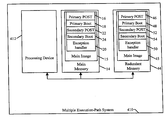
- FIG. 1 is a block diagram illustrating a multiple execution-path flash system 10 including a processor 12 and a main memory device 14 .
- the processor can be any type of computing device such as a microprocessor, application-specific integrated circuit (“ASIC”), field-programmable gate array (“FPGA”), or other programmable logic device (“PLD”).
- the main memory device 14 can be any type of non-volatile memory such as a flash memory device.
- the main memory device 14 includes a main flash image 15 including a primary power-on self test (“POST”) executable file (“post executable”) 16 , a primary Boot executable file (“boot executable”) 18 , a main exception handling executable file (“main exception handler”) 20 , a secondary post executable 22 , and a secondary Boot executable 24 .
- POST primary power-on self test
- post executable post executable
- boot executable boot executable
- main exception handling executable file main exception handler
- FIG. 2 a illustrates one embodiment of the processor according to the invention.
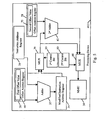
- the processor 12 a includes an instruction address register 26 , an offset address register 28 , a first offset bit 30 , and a first adder 32 for adding the content of the offset address register 28 to the content of the instruction address register 26 .
- the output of the first adder 32 is held in a modified instruction address register 34 and the offset bit controls a multiplexor (“mux”) 36 . If the first offset bit 30 is set, i.e., if the value of the first offset bit 30 is a logical high, the content of the modified instruction address register 34 is passed through the mux 36 to the memory management unit (“MMU”) 38 .
- MMU memory management unit
- FIG. 2 b illustrates another embodiment of the processor 12 b wherein the first offset bit 30 is used to multiplex the content of the offset address register 28 or a numeric value of zero into the adder 32 , with the output of the adder being sent to the MMU 38 .
- the switching mechanism is accomplished via the use of base address translation (“BAT”) registers that are maintained by system software. These processor registers take care of the logical to physical mapping of the execution address.
- BAT base address translation
- the primary and secondary executables 16 , 18 , 22 , 24 ( FIG. 1 ) are located within the memory device 14 at specific physical addresses.
- the starting addresses of the secondary executables are offset from the starting addresses of the primary executables by an amount equal to the content of the offset address register 28 ( FIG. 2 a ). If the value of the first offset bit 30 is a logic low, then the processor loads instructions from the primary executables 16 , 18 . If the value of the first offset bit 30 is a logic high, then the processor loads instructions from the secondary executables 22 , 24 .
- the main exception handler 20 sets the first offset bit 30 , resulting in control being passed to the secondary executables. Subsequently, if corrupt data is encountered in a secondary executable, the main exception handler resets the first offset bit 30 , allowing control to return to the primary executables. In this manner, a Boot process can complete, even if numerous instances of corrupt data exists in both the primary and secondary executables. The Boot process will only fail if corrupt data exists at the same relative addresses within the primary and secondary executables. This process is more fully illustrated by the multiple execution-path algorithm 100 as shown in FIG. 3 a.
- step 102 the offset bit 30 is initialized to a logic low and an offset value 40 is loaded into the offset address register 28 .
- step 104 the primary executables 16 , 18 are executed by the processor.
- step 106 an error condition is encountered.
- the main exception handler 20 sets the first offset bit 30 to a logic high in step 108 .
- step 110 control transfers to the secondary executables 22 , 24 .
- the flow chart of FIG. 3 b illustrates another embodiment of a multiple execution-path algorithm 200 similar to that shown in FIG. 2 a with the added steps of encountering an error condition while executing the secondary executables (step 212 ), resetting the first offset bit 30 to a logic low (step 214 ), and transferring control back to the primary executables (step 216 ).
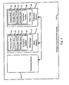
- FIG. 4 is a block diagram illustrating a multiple execution-path flash system 410 with a redundant memory device 44 .
- the redundant memory device 44 can be any type of non-volatile memory such as a flash memory device.
- the redundant memory device 44 includes a redundant flash image 45 including a primary power-on self test (“POST”) executable file (“post executable”) 46 , a primary Boot executable file (“boot executable”) 48 , a redundant exception handling executable file (“redundant exception handler”) 50 , a secondary post executable 52 , and a secondary Boot executable 54 .
- the processor 412 includes a second offset address register 58 , a second offset bit 60 , and a second adder 62 , as illustrated in FIG. 5 .
- the redundant memory device 44 has a starting physical address which is offset from the starting physical address of the main memory device 14 by a second offset value 70 .
- the second offset value 70 is held in the second offset address register 58 and is added to the output of the first adder 32 by the second adder 62 if the second offset bit 60 is a logic high.
- the second offset bit 60 controls the second multiplexor 66 , passing either the output of the first multiplexor 36 or the second adder 62 to the MMU 38 .
- the main exception handler 20 sets the second offset bit to a logic high if corrupted data is encountered at the same relative address within the primary and secondary executables 16 , 18 , 22 , 24 . In this manner, control is passed to the corresponding executables 46 , 48 , 52 , 54 within the redundant flash image 45 .
- a problem in the primary executables 46 , 48 will invoke the redundant exception handler 50 which will set the first offset bit 30 , resulting in control passing to the secondary executables 52 , 54 .
- a problem in the secondary executables 52 , 54 will result in the redundant exception handler 50 resetting the first offset bit 30 , returning control to the primary executables 46 , 48 .
- the redundant exception handler 50 will reset the second offset bit 60 , resulting in control passing to the executables 16 , 18 , 22 , 24 of the main flash image 15 .
- the Boot process will only fail if corrupt data exists at the same relative addresses within the primary and secondary executables of both the main and redundant flash images. This process is more fully illustrated by the multiple execution-path algorithm 300 as shown in FIG. 6 .
- step 302 corrupted information is encountered at the same relative addresses within the primary executables 16 , 18 and the secondary executables 22 , 24 of the main flash image 15 .
- step 304 the main exception 20 handler sets the second offset bit 60 resulting in control passing to the second flash image 45 .
- step 306 corrupted information is encountered at the same relative addresses within the primary executables 46 , 48 and the secondary executables 52 , 54 of the redundant flash image.
- step 308 the redundant exception handler 50 resets the second offset bit 60 resulting in control passing to the main flash image 15 .
- FIG. 7 Yet another embodiment of the invention is illustrated by the block diagram of FIG. 7 .
- the multiple execution-path flash system 510 is monitored by an external process 572 .
- This external process 572 may reside in a processing device within a general purpose computer, a server, or another embedded system such as an input/output adapter.
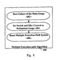
- a corresponding multiple execution-path algorithm 600 is illustrated in FIG. 8 .
- the external process 572 monitors the main exception handler 20 for an indication that both the primary executables 16 , 18 and the secondary executables 22 , 24 have failed at the same relative addresses. If this indication is detected by the external process 572 , the external process sets a switch 574 which transfers control from the main memory device 14 to the redundant memory device 44 in step 604 .
- step 606 the external process 572 resets the multiple execution-path flash system 510 , allowing the system to POST and Boot from the redundant memory device 44 . If the Boot from the redundant memory device fails, then the memory devices 14 , 44 must be reprogrammed or the multiple execution-path system 510 must be replaced.
Abstract
A multiple execution-path flash system includes a main flash image with primary and secondary POST and Boot executable files. The secondary executables are offset from the primary executables by a predetermined offset address. If corrupted data is encountered during Boot, the exception handler sets an offset bit resulting in the predetermined offset address being added to the current instruction address. If corrupted data is encountered in the secondary executables, the offset bit is reset. An optional redundant flash image may also be used. A failure at the same relative address in the primary and secondary executables of the main flash image will cause the exception handler to transfer control to the redundant flash image. A subsequent failure at the same relative address in the primary and secondary executables of the redundant flash image will cause the redundant exception handler to transfer control back to the main flash image.
Description
- This application a continuation of U.S. patent application Ser. No. 11/031,605 filed Jan. 7, 2005, the disclosure of which is hereby incorporated by reference as if set forth in its entirety herein.
- 1. Field of the Invention
- This invention is related in general to the field of bootable input/output adapters. In particular, the invention consists of a device for providing multiple alternate boot paths.
- 2. Description of the Prior Art
- In a digital processing system, input/output cards referred to as adapters are often used to communicate with devices external to the digital processing system. These adapters traditionally communicate with a central processor of the digital processing system or with each other through a data bus or network. An adapter may be an embedded system, i.e., may include a processing device that must be initialized during power-on and activation. During power-on self-test (“POST”), an adapter's hardware is exercised and diagnostics are performed. During Bootup, an adapter with an embedded processor will initialize the processor and other hardware external to the processor such as memory, and will perform an initial microcode load (“IML”).
- Executable programs are stored on the adapter and loaded into the processor during the Boot process. These executables may include a POST executable for performing the power-on self-test, a Kernel or Boot executable responsible for directing the Bootup, and an Exception Handler executable for identifying errors during the Boot process and taking corrective action.
- These executable programs are usually maintained in a memory device on the adapter. A common memory device used for this purpose is a Flash memory. The Flash memory is a non-volatile memory device that maintains its data, even when its power source has been turned off or disconnected. A traditional embedded system, such as an adapter, will include a flash image that includes the Kernel, POST, and exception handling executables. A system with a single-path flash includes a single flash image with only one Kernel executable, one POST executable, and one exception handling executable.
- A problem may occur if one or more memory locations within the Flash device contain erroneous information. This may occur if the one or more memory locations are defective, an external occurrence has caused the data in the memory locations to become corrupted, or if the process of programming the flash device was interrupted or aborted. Encountering a flash image problem in a single-path flash system requires that the flash be reprogrammed, that the flash device be replaced, or that the adapter possessing the flash device be replaced.
- One potential solution is to utilize a redundant flash image including a copy of the Kernel, POST, and exception handler executables. If corrupt information is encountered during the POST of Boot process of the primary flash image, the primary exception handling executable will switch control to the redundant flash image. If the redundant flash image is viable, the POST and Boot processes are loaded into the processor and executed. Alternatively, the Boot and POST processes of the embedded system may be monitored by an external device, such as another adapter or embedded system. If the primary exception handling executable generates an error message, the external device may swap the redundant flash image for the primary flash image and reset the adapter. However, the process of swapping image files and resetting the adapter may take a significant amount of time. Additionally, if the redundant flash image is also corrupted, the adapter will fail to execute its POST and Boot executables requiring that the flash images be programmed, the flash devices be replaced, or the adapter be replaced. Accordingly, it would be advantageous to have a system for providing an alternate boot path that does not require swapping a primary flash image with a redundant flash image. Additionally, it is desirable to have a system for booting from flash images, even if all the flash images include areas of corrupted information.
- The invention disclosed herein utilizes a multiple execution-path flash system to allow for successful loading of executable files. A main flash image includes a primary POST executable, a primary Boot executable, and an exception handling executable. Additionally, the main flash image includes a secondary POST executable and a secondary Boot executable, both of which are offset from their corresponding primary executables by a predetermined offset address. If an error condition occurs when loading either the primary POST executable or the primary Boot executable, the exception handling executable will set an offset bit. If the offset bit has been set, a predetermined offset address will be added to the current instruction address being loaded by the processor, resulting in instructions being loaded into the process from a secondary executable.
- If another error condition occurs during the execution of the secondary executables, the exception handling executable will reset the offset bit. The current instruction address will not be offset by the predetermined offset address and control will return to the primary executables. In this manner, multiple data corruptions may be encountered without interrupting the POST and Boot processes.
- If both the primary executables and the secondary executables contain corrupt information at the same relative locations, the exception handler cannot overcome an execution problem by setting or resetting the offset bit. Rather, the exception handler must turn control over to a redundant flash image. Alternatively, an external process may recognize an error code generated by the exception handler, swap the redundant flash image with the primary flash image, and reset the adapter. If the redundant flash image also includes a multiple-path execution path, corrupted data within the redundant flash image may be bypassed as in the primary flash image.
- Yet another advantage of the invention is realized if corrupted data is encountered at the same relative addresses of the primary and secondary executables within the redundant flash image. If this occurs, the exception handling executable within the redundant flash image can turn control back over to the main flash image. Alternatively, an external process may recognize the error code generated by the redundant exception handler and swap the redundant flash image with the main flash image again, returning control to the main flash image after resetting the adapter.
- If control is transferable between the main and redundant flash images without resetting the adapter, the POST and Boot processes will complete unless corrupted information is encountered at the same relative memory locations within the primary and second executables of both the main and redundant flash images. If the adapter must be reset after transferring control between the main and redundant flash images, then the POST and Boot processes will complete unless corrupted information is encountered at first relative memory locations within the primary and secondary executables of the main flash image and corrupted information is encountered at second relative memory locations within the primary and secondary executables of the redundant flash image.
- Various other purposes and advantages of the invention will become clear from its description in the specification that follows and from the novel features particularly pointed out in the appended claims. Therefore, to the accomplishment of the objectives described above, this invention comprises the features hereinafter illustrated in the drawings, fully described in the detailed description of the preferred embodiments and particularly pointed out in the claims. However, such drawings and description disclose just a few of the various ways in which the invention may be practiced.
-
FIG. 1 is a block diagram illustrating a multiple execution-path flash system including a processor and a main memory device. -
FIG. 2 a is a block diagram illustrating a first embodiment of the processor ofFIG. 1 . -
FIG. 2 b is a block diagram illustrating a second embodiment of the processor ofFIG. 1 . -
FIG. 3 a is a flow chart illustrating a multiple execution-path algorithm utilizing primary and secondary executables according to the invention. -
FIG. 3 b is a flow chart illustrating the algorithm ofFIG. 3 a with the added step of returning control back to the primary executables. -
FIG. 4 is a block diagram illustrating the multiple execution-path flash system ofFIG. 1 including a redundant memory device. -
FIG. 5 is a block diagram of the processor of the multiple execution-path flash system ofFIG. 4 . -
FIG. 6 is a flow chart illustrating a multiple execution-path algorithm utilizing main and redundant memory devices according to the invention. -
FIG. 7 is a block diagram of a multiple execution-path system including an external process and a switch. - This invention is based on the idea of using a multiple execution-path flash system. The invention disclosed herein may be implemented as a method, apparatus or article of manufacture using standard programming or engineering techniques to produce software, firmware, hardware, or any combination thereof. The term “article of manufacture” as used herein refers to code or logic implemented in hardware or computer readable media such as optical storage devices, and volatile or non-volatile memory devices. Such hardware may include, but is not limited to, field programmable gate arrays (“FPGAs”), application-specific integrated circuits (“ASICs”), complex programmable logic devices (“CPLDs”), programmable logic arrays (“PLAs”), microprocessors, or other similar processing devices.
- Referring to figures, wherein like parts are designated with the same reference numerals and symbols,
FIG. 1 is a block diagram illustrating a multiple execution-path flash system 10 including aprocessor 12 and amain memory device 14. The processor can be any type of computing device such as a microprocessor, application-specific integrated circuit (“ASIC”), field-programmable gate array (“FPGA”), or other programmable logic device (“PLD”). Themain memory device 14 can be any type of non-volatile memory such as a flash memory device. Themain memory device 14 includes amain flash image 15 including a primary power-on self test (“POST”) executable file (“post executable”) 16, a primary Boot executable file (“boot executable”) 18, a main exception handling executable file (“main exception handler”) 20, asecondary post executable 22, and asecondary Boot executable 24. -
FIG. 2 a illustrates one embodiment of the processor according to the invention. Theprocessor 12 a includes aninstruction address register 26, an offsetaddress register 28, a first offsetbit 30, and afirst adder 32 for adding the content of the offsetaddress register 28 to the content of theinstruction address register 26. In this embodiment of the invention, the output of thefirst adder 32 is held in a modifiedinstruction address register 34 and the offset bit controls a multiplexor (“mux”) 36. If the first offsetbit 30 is set, i.e., if the value of the first offsetbit 30 is a logical high, the content of the modifiedinstruction address register 34 is passed through themux 36 to the memory management unit (“MMU”) 38. Otherwise, the content of theinstruction address register 26 is passed to theMMU 38.FIG. 2 b illustrates another embodiment of theprocessor 12 b wherein the first offsetbit 30 is used to multiplex the content of the offsetaddress register 28 or a numeric value of zero into theadder 32, with the output of the adder being sent to theMMU 38. In an embedded processor, the switching mechanism is accomplished via the use of base address translation (“BAT”) registers that are maintained by system software. These processor registers take care of the logical to physical mapping of the execution address. - The primary and
secondary executables FIG. 1 ) are located within thememory device 14 at specific physical addresses. The starting addresses of the secondary executables are offset from the starting addresses of the primary executables by an amount equal to the content of the offset address register 28 (FIG. 2 a). If the value of the first offsetbit 30 is a logic low, then the processor loads instructions from theprimary executables bit 30 is a logic high, then the processor loads instructions from thesecondary executables - If corrupt data is encountered in a primary executable, the
main exception handler 20 sets the first offsetbit 30, resulting in control being passed to the secondary executables. Subsequently, if corrupt data is encountered in a secondary executable, the main exception handler resets the first offsetbit 30, allowing control to return to the primary executables. In this manner, a Boot process can complete, even if numerous instances of corrupt data exists in both the primary and secondary executables. The Boot process will only fail if corrupt data exists at the same relative addresses within the primary and secondary executables. This process is more fully illustrated by the multiple execution-path algorithm 100 as shown inFIG. 3 a. - In step 102, the offset
bit 30 is initialized to a logic low and an offsetvalue 40 is loaded into the offsetaddress register 28. Instep 104, theprimary executables step 106, an error condition is encountered. Themain exception handler 20 sets the first offsetbit 30 to a logic high instep 108. Instep 110, control transfers to thesecondary executables FIG. 3 b illustrates another embodiment of a multiple execution-path algorithm 200 similar to that shown inFIG. 2 a with the added steps of encountering an error condition while executing the secondary executables (step 212), resetting the first offsetbit 30 to a logic low (step 214), and transferring control back to the primary executables (step 216). -
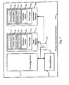
FIG. 4 is a block diagram illustrating a multiple execution-path flash system 410 with aredundant memory device 44. Theredundant memory device 44 can be any type of non-volatile memory such as a flash memory device. Theredundant memory device 44 includes aredundant flash image 45 including a primary power-on self test (“POST”) executable file (“post executable”) 46, a primary Boot executable file (“boot executable”) 48, a redundant exception handling executable file (“redundant exception handler”) 50, asecondary post executable 52, and asecondary Boot executable 54. Additionally, theprocessor 412 includes a second offsetaddress register 58, a second offsetbit 60, and asecond adder 62, as illustrated inFIG. 5 . - The
redundant memory device 44 has a starting physical address which is offset from the starting physical address of themain memory device 14 by a second offsetvalue 70. The second offsetvalue 70 is held in the second offsetaddress register 58 and is added to the output of thefirst adder 32 by thesecond adder 62 if the second offsetbit 60 is a logic high. The second offsetbit 60 controls thesecond multiplexor 66, passing either the output of thefirst multiplexor 36 or thesecond adder 62 to theMMU 38. In this embodiment of the invention, themain exception handler 20 sets the second offset bit to a logic high if corrupted data is encountered at the same relative address within the primary andsecondary executables executables redundant flash image 45. - As with the
main flash image 15, a problem in theprimary executables redundant exception handler 50 which will set the first offsetbit 30, resulting in control passing to thesecondary executables secondary executables redundant exception handler 50 resetting the first offsetbit 30, returning control to theprimary executables primary executables secondary executable redundant exception handler 50 will reset the second offsetbit 60, resulting in control passing to theexecutables main flash image 15. In this embodiment of the invention, the Boot process will only fail if corrupt data exists at the same relative addresses within the primary and secondary executables of both the main and redundant flash images. This process is more fully illustrated by the multiple execution-path algorithm 300 as shown inFIG. 6 . - In
step 302, corrupted information is encountered at the same relative addresses within theprimary executables secondary executables main flash image 15. Instep 304, themain exception 20 handler sets the second offsetbit 60 resulting in control passing to thesecond flash image 45. Instep 306, corrupted information is encountered at the same relative addresses within theprimary executables secondary executables step 308, theredundant exception handler 50 resets the second offsetbit 60 resulting in control passing to themain flash image 15. - Yet another embodiment of the invention is illustrated by the block diagram of
FIG. 7 . The multiple execution-path flash system 510 is monitored by anexternal process 572. Thisexternal process 572 may reside in a processing device within a general purpose computer, a server, or another embedded system such as an input/output adapter. A corresponding multiple execution-path algorithm 600 is illustrated inFIG. 8 . Instep 602, theexternal process 572 monitors themain exception handler 20 for an indication that both theprimary executables secondary executables external process 572, the external process sets aswitch 574 which transfers control from themain memory device 14 to theredundant memory device 44 instep 604. Instep 606, theexternal process 572 resets the multiple execution-path flash system 510, allowing the system to POST and Boot from theredundant memory device 44. If the Boot from the redundant memory device fails, then thememory devices path system 510 must be replaced. - Those skilled in the art of making systems that POST and Boot from non-volatile memory may develop other embodiments of the present invention. However, the terms and expressions which have been employed in the foregoing specification are used therein as terms of description and not of limitation, and there is no intention in the use of such terms and expressions of excluding equivalents of the features shown and described or portions thereof, it being recognized that the scope of the invention is defined and limited only by the claims which follow.
Claims (13)
1. A multiple execution-path system, comprising:
a processing device; and
a main memory device storing a main image including a main primary Boot executable file, a main secondary Boot executable file that is identical to the primary Boot executable file upon being written to the main memory device and is offset from the main primary Boot executable file by an offset value, and a main exception handling executable file;
wherein the main exception handling executable file is adapted to identify a first error condition indicative of corrupted information in the main primary Boot executable file and to transfer a control of a Boot process from the main primary Boot executable file to the main secondary Boot executable file.
2. The multiple execution-path system of claim 1 , wherein the processing device is an embedded processor.
3. The multiple execution-path system of claim 1 , wherein the main memory device is a flash memory device.
4. The multiple execution-path system of claim 1 , wherein the processing device includes an offset bit.
5. The multiple execution-path system of claim 1 , wherein the main exception handling executable file is further adapted to identify a second error condition indicative of corrupted information in the main secondary Boot executable file and to transfer the control of the Boot process from the main secondary Boot executable file to the main primary Boot executable file.
6. The multiple execution-path system of claim 1 , further comprising a redundant memory device including a redundant image and wherein the main exception handling executable file is adapted to identify a third error condition indicative of corrupted information in the main primary Boot executable file and at a first same relative location within the main secondary Boot executable file and to transfer the control of the Boot process from the main image to the redundant image.
7. The multiple execution-path system of claim 6 , wherein the redundant image includes a redundant primary executable file, a redundant secondary executable file, and a redundant exception handling executable file adapted to identify a fourth error condition indicative of corrupted information in the redundant primary Boot executable file and at a second same relative location within the redundant secondary Boot executable file and to transfer the control of the Boot process from the redundant image to the main image.
8. The multiple execution-path system of claim 6 , further comprising an external process for identifying a first error message generated by the main exception handling executable file indicative of the third error condition, said external process being adapted to set a switch effecting the transfer and to reset the multiple execution-path system.
9. An article of manufacture including a data storage medium, said data storage medium including a set of machine-readable instructions that are executable by a processing device to implement an algorithm, said algorithm comprising the steps of:
detecting corrupt information within a main primary executable file residing in a main image within a main memory device; and
transferring a control of a Boot process from the main primary executable file to a main secondary executable file residing in the main image, wherein the main secondary executable file is identical to the main primary executable file upon being written to the main memory device.
10. The article of manufacture of claim 9 , further comprising the steps of:
detecting corrupt information within the main secondary executable file; and
transferring the control of the Boot process from the main secondary executable file to a main primary executable file residing in the main image.
11. The article of manufacture of claim 9 , further comprising the steps of:
detecting corrupt information within the main secondary executable file; and
transferring the control of the Boot process from the main image to a redundant image.
12. The article of manufacture of claim 10 , further comprising the steps of:
detecting corrupt information at a first location within the main primary executable file and a first same relative location within the main secondary executable file; and
transferring the control of the Boot process from the main image to a redundant image.
13. The article of manufacture of claim 12 , further comprising the steps of:
detecting corrupt information at a second location within a redundant primary executable file and a second same relative location within a redundant secondary executable file; and
transferring the control of the Boot process from the redundant image to the main image.
Priority Applications (1)
| Application Number | Priority Date | Filing Date | Title |
|---|---|---|---|
| US11/960,440 US20080098257A1 (en) | 2005-01-07 | 2007-12-19 | Multiple Execution-Path System |
Applications Claiming Priority (2)
| Application Number | Priority Date | Filing Date | Title |
|---|---|---|---|
| US11/031,605 US7340595B2 (en) | 2005-01-07 | 2005-01-07 | Multiplex execution-path system |
| US11/960,440 US20080098257A1 (en) | 2005-01-07 | 2007-12-19 | Multiple Execution-Path System |
Related Parent Applications (1)
| Application Number | Title | Priority Date | Filing Date |
|---|---|---|---|
| US11/031,605 Continuation US7340595B2 (en) | 2005-01-07 | 2005-01-07 | Multiplex execution-path system |
Publications (1)
| Publication Number | Publication Date |
|---|---|
| US20080098257A1 true US20080098257A1 (en) | 2008-04-24 |
Family
ID=36654635
Family Applications (2)
| Application Number | Title | Priority Date | Filing Date |
|---|---|---|---|
| US11/031,605 Expired - Fee Related US7340595B2 (en) | 2005-01-07 | 2005-01-07 | Multiplex execution-path system |
| US11/960,440 Abandoned US20080098257A1 (en) | 2005-01-07 | 2007-12-19 | Multiple Execution-Path System |
Family Applications Before (1)
| Application Number | Title | Priority Date | Filing Date |
|---|---|---|---|
| US11/031,605 Expired - Fee Related US7340595B2 (en) | 2005-01-07 | 2005-01-07 | Multiplex execution-path system |
Country Status (1)
| Country | Link |
|---|---|
| US (2) | US7340595B2 (en) |
Cited By (3)
| Publication number | Priority date | Publication date | Assignee | Title |
|---|---|---|---|---|
| US20090138754A1 (en) * | 2007-11-28 | 2009-05-28 | David Alan Edwards | Memory Errors |
| US20100235618A1 (en) * | 2009-03-11 | 2010-09-16 | Harman Becker Automotive Systems Gmbh | Start-up of computing systems |
| US20170046229A1 (en) * | 2015-08-13 | 2017-02-16 | Quanta Computer Inc. | Dual boot computer system |
Families Citing this family (13)
| Publication number | Priority date | Publication date | Assignee | Title |
|---|---|---|---|---|
| US7676671B2 (en) * | 2006-10-31 | 2010-03-09 | Hewlett-Packard Development Company, L.P. | System for multi-profile boot selection of an embedded device |
| US8449467B2 (en) * | 2006-11-28 | 2013-05-28 | Siemens Medical Solutions Usa, Inc. | Helical acoustic array for medical ultrasound |
| ATE528761T1 (en) * | 2009-11-02 | 2011-10-15 | Giga Byte Tech Co Ltd | FLASH MEMORY ACCESS DEVICE AND METHOD THEREOF |
| US8793526B2 (en) | 2011-10-25 | 2014-07-29 | International Business Machines Corporation | Firmware management in a computing system |
| CN105122214B (en) * | 2013-04-23 | 2019-03-01 | 惠普发展公司,有限责任合伙企业 | Reparation to the system data damaged in nonvolatile memory |
| WO2014175862A1 (en) | 2013-04-23 | 2014-10-30 | Hewlett-Packard Development Company, L.P. | Redundant system boot code in a secondary non-volatile memory |
| US10733288B2 (en) | 2013-04-23 | 2020-08-04 | Hewlett-Packard Development Company, L.P. | Verifying controller code and system boot code |
| CN103473098A (en) * | 2013-09-10 | 2013-12-25 | 华为技术有限公司 | Starting method of boot program and relevant device |
| FR3055714B1 (en) * | 2016-09-08 | 2018-09-28 | Continental Automotive France | ERROR CORRECTION METHOD IN A FLASH MEMORY |
| JP7330681B2 (en) * | 2018-10-04 | 2023-08-22 | キヤノン株式会社 | Information processing apparatus, its control method, program, and image forming apparatus |
| WO2020159533A1 (en) | 2019-02-01 | 2020-08-06 | Hewlett-Packard Development Company, L.P. | Security credential derivation |
| WO2020167283A1 (en) | 2019-02-11 | 2020-08-20 | Hewlett-Packard Development Company, L.P. | Recovery from corruption |
| TWI722852B (en) * | 2020-03-30 | 2021-03-21 | 技嘉科技股份有限公司 | Solid-state disk and startup method |
Citations (9)
| Publication number | Priority date | Publication date | Assignee | Title |
|---|---|---|---|---|
| US6205548B1 (en) * | 1998-07-31 | 2001-03-20 | Intel Corporation | Methods and apparatus for updating a nonvolatile memory |
| US20030005277A1 (en) * | 2001-06-29 | 2003-01-02 | Harding Matthew C. | Automatic replacement of corrupted BIOS image |
| US6754818B1 (en) * | 2000-08-31 | 2004-06-22 | Sun Microsystems, Inc. | Method and system for bootstrapping from a different boot image when computer system is turned on or reset |
| US6757838B1 (en) * | 2000-10-13 | 2004-06-29 | Hewlett-Packard Development Company, L.P. | Hardware independent implementation of computer system BIOS recovery |
| US6892323B2 (en) * | 1999-05-05 | 2005-05-10 | Giga-Byte Technology Co., Ltd. | Dual basic input/output system for a computer |
| US6957328B2 (en) * | 2001-01-05 | 2005-10-18 | International Business Machines Corporation | System and method using a first counter and a second counter to select a code image during a reboot routine |
| US7024581B1 (en) * | 2002-10-09 | 2006-04-04 | Xpoint Technologies, Inc. | Data processing recovery system and method spanning multiple operating system |
| US7206971B2 (en) * | 2003-04-07 | 2007-04-17 | Lsi Logic Corporation | Selectable and updatable computer boot memory |
| US7219221B2 (en) * | 2003-06-03 | 2007-05-15 | Hon Hai Precision Ind. Co., Ltd. | System and method for automatic booting based on single flash ROM |
-
2005
- 2005-01-07 US US11/031,605 patent/US7340595B2/en not_active Expired - Fee Related
-
2007
- 2007-12-19 US US11/960,440 patent/US20080098257A1/en not_active Abandoned
Patent Citations (9)
| Publication number | Priority date | Publication date | Assignee | Title |
|---|---|---|---|---|
| US6205548B1 (en) * | 1998-07-31 | 2001-03-20 | Intel Corporation | Methods and apparatus for updating a nonvolatile memory |
| US6892323B2 (en) * | 1999-05-05 | 2005-05-10 | Giga-Byte Technology Co., Ltd. | Dual basic input/output system for a computer |
| US6754818B1 (en) * | 2000-08-31 | 2004-06-22 | Sun Microsystems, Inc. | Method and system for bootstrapping from a different boot image when computer system is turned on or reset |
| US6757838B1 (en) * | 2000-10-13 | 2004-06-29 | Hewlett-Packard Development Company, L.P. | Hardware independent implementation of computer system BIOS recovery |
| US6957328B2 (en) * | 2001-01-05 | 2005-10-18 | International Business Machines Corporation | System and method using a first counter and a second counter to select a code image during a reboot routine |
| US20030005277A1 (en) * | 2001-06-29 | 2003-01-02 | Harding Matthew C. | Automatic replacement of corrupted BIOS image |
| US7024581B1 (en) * | 2002-10-09 | 2006-04-04 | Xpoint Technologies, Inc. | Data processing recovery system and method spanning multiple operating system |
| US7206971B2 (en) * | 2003-04-07 | 2007-04-17 | Lsi Logic Corporation | Selectable and updatable computer boot memory |
| US7219221B2 (en) * | 2003-06-03 | 2007-05-15 | Hon Hai Precision Ind. Co., Ltd. | System and method for automatic booting based on single flash ROM |
Cited By (8)
| Publication number | Priority date | Publication date | Assignee | Title |
|---|---|---|---|---|
| US20090138754A1 (en) * | 2007-11-28 | 2009-05-28 | David Alan Edwards | Memory Errors |
| US7996711B2 (en) * | 2007-11-28 | 2011-08-09 | Icera Inc. | Memory errors |
| US20110283136A1 (en) * | 2007-11-28 | 2011-11-17 | Icera Inc. | Memory errors |
| US8479039B2 (en) * | 2007-11-28 | 2013-07-02 | Icera Inc. | Memory errors |
| US20100235618A1 (en) * | 2009-03-11 | 2010-09-16 | Harman Becker Automotive Systems Gmbh | Start-up of computing systems |
| US8621193B2 (en) * | 2009-03-11 | 2013-12-31 | Harman Becker Automotive Systems Gmbh | Booting a computer system at start-up by transferring a first part of instructions using a second bus and transferring a second part of instructions using a first bus where the second bus is configured to transfer instructions at a faster rate than the first bus |
| US20170046229A1 (en) * | 2015-08-13 | 2017-02-16 | Quanta Computer Inc. | Dual boot computer system |
| US10191811B2 (en) * | 2015-08-13 | 2019-01-29 | Quanta Computer Inc. | Dual boot computer system |
Also Published As
| Publication number | Publication date |
|---|---|
| US20060155979A1 (en) | 2006-07-13 |
| US7340595B2 (en) | 2008-03-04 |
Similar Documents
| Publication | Publication Date | Title |
|---|---|---|
| US7340595B2 (en) | Multiplex execution-path system | |
| US7900036B2 (en) | System and method for implementing boot/recovery on a data processing sysem | |
| US8166338B2 (en) | Reliable exception handling in a computer system | |
| US20120110562A1 (en) | Synchronized firmware update | |
| CN100549946C (en) | Be used to carry out the apparatus and method of data processing operation | |
| US20180031632A1 (en) | Hardware debug host | |
| US10909247B2 (en) | Computing device having two trusted platform modules | |
| US20070174704A1 (en) | Computer program automatic recovery activation control method and system | |
| TW201106151A (en) | Detection of uncorrectable re-grown fuses in a microprocessor | |
| US11099949B2 (en) | Method apparatus for resuming and recovery checking from interrupted programming of one-time programmable memory device | |
| US8826080B2 (en) | Methods and systems for preboot data verification | |
| US8234543B2 (en) | Detection and correction of fuse re-growth in a microprocessor | |
| US11379330B2 (en) | Information handling systems and related methods for testing memory during boot and during operating system (OS) runtime | |
| JP2012198876A (en) | Device and method for curing read inability state in memory device | |
| US8555050B2 (en) | Apparatus and method thereof for reliable booting from NAND flash memory | |
| US20220308963A1 (en) | Method and apparatus for providing recovery from a computing device boot up error | |
| US20050033954A1 (en) | Computer system having BIOS with multiple memory block | |
| CN111221675B (en) | Method and apparatus for self-diagnosis of RAM error detection logic | |
| US10846421B2 (en) | Method for protecting unauthorized data access from a memory | |
| US20040225792A1 (en) | Computer system | |
| EP3525210B1 (en) | Data register monitoring | |
| US20080215870A1 (en) | Method and apparatus for loading boot code | |
| US7480836B2 (en) | Monitoring error-handler vector in architected memory | |
| US7165172B1 (en) | Facilitating cold reset and warm reset tasking in a computer system | |
| US8151176B2 (en) | CPU instruction RAM parity error procedure |
Legal Events
| Date | Code | Title | Description |
|---|---|---|---|
| STCB | Information on status: application discontinuation |
Free format text: ABANDONED -- FAILURE TO PAY ISSUE FEE |