US20080098271A1 - System and Method for Verification and Generation of Timing Exceptions - Google Patents
System and Method for Verification and Generation of Timing Exceptions Download PDFInfo
- Publication number
- US20080098271A1 US20080098271A1 US11/876,903 US87690307A US2008098271A1 US 20080098271 A1 US20080098271 A1 US 20080098271A1 US 87690307 A US87690307 A US 87690307A US 2008098271 A1 US2008098271 A1 US 2008098271A1
- Authority
- US
- United States
- Prior art keywords
- logic circuit
- exceptions
- representation
- timing
- verifying
- Prior art date
- Legal status (The legal status is an assumption and is not a legal conclusion. Google has not performed a legal analysis and makes no representation as to the accuracy of the status listed.)
- Granted
Links
Images


Classifications
-
- G—PHYSICS
- G01—MEASURING; TESTING
- G01R—MEASURING ELECTRIC VARIABLES; MEASURING MAGNETIC VARIABLES
- G01R31/00—Arrangements for testing electric properties; Arrangements for locating electric faults; Arrangements for electrical testing characterised by what is being tested not provided for elsewhere
- G01R31/28—Testing of electronic circuits, e.g. by signal tracer
- G01R31/317—Testing of digital circuits
- G01R31/31727—Clock circuits aspects, e.g. test clock circuit details, timing aspects for signal generation, circuits for testing clocks
-
- G—PHYSICS
- G01—MEASURING; TESTING
- G01R—MEASURING ELECTRIC VARIABLES; MEASURING MAGNETIC VARIABLES
- G01R31/00—Arrangements for testing electric properties; Arrangements for locating electric faults; Arrangements for electrical testing characterised by what is being tested not provided for elsewhere
- G01R31/28—Testing of electronic circuits, e.g. by signal tracer
- G01R31/317—Testing of digital circuits
- G01R31/31725—Timing aspects, e.g. clock distribution, skew, propagation delay
-
- G—PHYSICS
- G06—COMPUTING; CALCULATING OR COUNTING
- G06F—ELECTRIC DIGITAL DATA PROCESSING
- G06F30/00—Computer-aided design [CAD]
- G06F30/30—Circuit design
- G06F30/32—Circuit design at the digital level
- G06F30/33—Design verification, e.g. functional simulation or model checking
- G06F30/3308—Design verification, e.g. functional simulation or model checking using simulation
- G06F30/3312—Timing analysis
-
- G—PHYSICS
- G06—COMPUTING; CALCULATING OR COUNTING
- G06F—ELECTRIC DIGITAL DATA PROCESSING
- G06F2119/00—Details relating to the type or aim of the analysis or the optimisation
- G06F2119/12—Timing analysis or timing optimisation
Definitions
- the present invention relates to the field of digital circuits.
- the present invention relates to the verification of digital circuits.
- Digital or logic circuits are implemented in almost any electronic device available today and offer the possibility of integrating an increasing number of functions and features into devices without raising production costs considerably.
- the number of circuit elements and thereby the complexity of the digital or logic circuits has increased. Consequently, the effort undertaken to design the digital or logic circuits has enormously increased.
- the verification methods analyse the function and/or the layout of the design of the chip layout in order to simulate the function of the chip.
- Different types of the verification methods i.e. timing verification or functional verification methods, are currently known in the art.
- the aim of static timing analysis is to verify that a logic circuit, in particular a digital circuit, satisfies its timing constraints, i.e. that the logic circuit will function correctly when run at an intended speed.
- Timing exceptions are typically used for specifying paths to be false paths or to be multi-cycle paths. The timing exceptions are typically provided by the user of static timing analysis tools.
- Timing violations have the effect that those timing violations, which are specified to be exceptional, are simply ignored by the static timing analysis tool. It is evident that this procedure is error-prone. For example, static timing analysis may ignore relevant timing violations if the timing violation has been wrongly specified to be a timing exception, termed invalid timing exception which can lead to operational malfunction of the logic circuit. Timing violations that are correctly specified as timing exceptions are termed valid timing exception.
- U.S. Pat. No. 5,638,290 describes a method for removing critical false paths during logic optimization based on a redundancy removal algorithm using essentially thee steps: starting a timing verification, searching for critical paths, extracting critical cones. This method has to be iteratively repeated for as long as a critical path is false.
- a method for verifying one or more exceptions in a logic circuit comprising: a first step of providing an initial representation of a logic circuit, a second step of indicating at least one exception for the logic circuit, a third step of introducing one or more potential malfunctions of the logic circuit related to the one or more timing exceptions into the initial representation of the logic circuit to produce a modified representation of the logic circuit, a fourth step of determining whether functional behaviour of the modified representation of the logic circuit differs from functional behaviour of the initial representation of the logic circuit, and a fifth step of reporting a result relating to the difference in the functional behaviour of the modified representation of the logic circuit from the functional behaviour of the initial representation of the logic circuit.
- the method according to the invention verifies a set of exceptions in an efficient and automated way.
- an exception that is verified may be considered a valid exception and an exception that can not be verified may be considered invalid.
- the first representation of the logic circuit may thereby be in a description format known in the art such as an RTL or net list format, but other representations or description formats for a logic circuit may be used.
- the one or more exceptions are timing exceptions.
- the exceptions may also be any timing violation in the logic circuit.
- the invention may be advantageously applied for the verification of timing exceptions of a logic circuit.
- the one or more exceptions are clock domain crossings or similar.
- Timing exceptions which have been verified to be valid may be safely used by known procedures such as static timing analysis (STA) tools, place and route tools, or other tools.
- STA static timing analysis
- an exception or a timing exception may be verified by introducing a potential malfunction into the representation of the logic circuits.
- the potential malfunction may be introduced by modifying the representation of the logic circuit, especially by duplicating shared parts of the logic and adding switches and new inputs which allow conditional fault induction to one of the duplicate logics while the other of the duplicate logics maintains its original functionality. It can be checked or verified, whether inducing a fault by switching on or off of the malfunction of the logic circuit in the modified representation has an influence on the function of the logic circuit, i.e. whether the functional behaviour of the logic circuit described by the modified representation differs from the function of the logic circuit described by the unmodified description.
- the exception may also be verified for a particular use of the logic circuit.
- the importance and/or validity of an exception may be different for different uses of the logic circuit. Thus an exception may be true in some instances while the exception is false in others.
- the malfunctions are caused by the exceptions.
- the result in the fifth step indicates whether each of the one or more exceptions is acceptable for the initial representation of the logic circuit or reporting a sequence of events showing a faulty behaviour of the initial representation of the logic circuit under and/or for the indicated exception.
- At least a section of the circuit is represented by a directed acyclic graph comprising nodes and edges, and defining paths through the nodes, wherein each path runs from an input node to an output node.
- the one or more timing exception defines a set of paths, the set comprising one or more timing exception paths.
- the one or more timing exception paths may comprise false paths or multi cycle paths but can be any type of path running between two nodes.
- the two nodes may thereby be input and/or output nodes of the logic circuit, but can be in principle any node of the represented circuit.
- a timing exception may thus be either a false path exception or a multi cycle path exception.
- the third step further comprises duplicating the nodes and/or edges in the representation of the logic circuit until every input node of the modified representation of the logic circuit is either a start point of one of the timing exceptions paths or a start point of one of a non-timing exception paths.
- the initial representation of the logic circuit is modified into a modified representation that can be easily separated into at least two parts.
- One part of the modified representation does not contain any path specified as timing exception.
- Another part of the modified representation contains solely paths specified as timing exception.
- the functional behaviour of the initial representation of the logic circuit and/or the modified representation of the logic circuit is defined in terms of 3-valued (X-valued) simulation comprising gate delay times and net delay times.
- the method comprises one or more multiplexer switches to introduce the malfunction into the representation of the logic circuit.
- Multiplexer switches may be integrated into the modified representation of the logic circuit in order to switch on and/or off introduction of fault values along paths or sections of the logic circuit for determining the function of the logic circuit, i.e. whether the timing exceptions modify the functional behaviour of the logic circuit.
- Using a plurality of multiplexer switches introduced at different places in the representation of the logic circuit allows the verification of a plurality of combinations of timing exceptions.
- a plurality of initial representations of the logic circuit and modified representation of the logic circuit are connected sequentially to represent a multiple cycle simulation.
- the timing exception may herein comprise multi-cycle paths.
- a static 3-valued model is defined and at least one formal verification method is used to determine whether the functional behaviour of the modified representation of the logic circuit differs from the functional behaviour of the initial representation of the logic circuit.
- timing exceptions are grouped in subcategories of timing exceptions, one subcategory of timing exceptions for multi-cycle paths of same cycle length and identical start point, and/or one or more subcategories containing false paths, so that a static model for potential sequential malfunction can be constructed.
- the third step may further comprise duplicating the nodes and/or edges in the representation of the logic circuit until every input node of the modified representation of the logic circuit is either a start point of a false path, a start point of one subcategory of multi-cycle path or a start point of non timing exceptions paths.
- the logic circuit represented may be a section of an integrated circuit.
- a complete integrated circuit can also be represented.
- the invention is also advantageously applied in a method for verifying logic circuits comprising the steps of generating a representation of a logic circuit, identifying timing exception for the logic circuits verifying the timing exceptions using the method according to any of the embodiments of the invention discussed above.
- the method may also be used in a computer program product that allows for execution on a computer.
- the present invention is a method for verifying one or more exceptions in a logic circuit, the method comprising the steps of providing an initial representation of a logic circuit, indicating at least one exception for the logic circuit, introducing one or more potential malfunctions of the logic circuit related to the one or more exceptions into the representation of the logic circuit to produce a modified representation of the logic circuit, determining whether functional behaviour of the modified representation of the logic circuit differs from functional behaviour of the first representation of the logic circuit, and reporting a result relating to the difference in the functional behaviour of the modified representation of the logic circuit from the functional behaviour of the initial representation of the logic circuit.
- the one or more exceptions may be, for example, timing exceptions.
- the malfunction may be caused by the indicated one or more exceptions.
- the result in the reporting step indicates whether each of the one or more exceptions is acceptable for the initial representation of the logic circuit or reporting a sequence of events showing a faulty behaviour of the initial representation of the logic circuit for the indicated exception.
- at least a section of the circuit may be represented by a directed acyclic graph comprising nodes and edges, and defining paths through the nodes, wherein each path runs from an input node to an output node.
- the one or more exceptions are timing exceptions and the one or more timing exception defines a set of paths, the set comprising one or more timing exception path.
- the one or more timing exception paths may comprise false paths.
- introducing step further comprises duplicating the nodes and/or edges in the representation of the logic circuit until every input node of the modified representation of the logic circuit is either a start point of timing exceptions paths or a start point of non timing exceptions paths.
- the functional behaviour of the initial representation of the logic circuit and/or the modified representation of the logic circuit is defined in terms of 3-valued (X-valued) simulation comprising gate delay times and net delay times.
- the method further comprises one or more multiplexer switches to introduce the malfunction into the representation of the logic circuit.
- a plurality of initial representations of the logic circuit and modified representation of the logic circuit may be connected sequentially to represent a multiple cycle simulation.
- the one or more timing exception may define a set of paths, the set comprising one or more timing exception path and wherein the timing exception paths comprise multi-cycle paths. Further, a static 3-valued model may be defined and at least one formal verification method is used to determine whether the functional behaviour of the modified representation of the logic circuit differs from the functional behaviour of the initial representation of the logic circuit.
- the one or more exceptions are timing exceptions and the one or more timing exception defines a set of paths, the set comprising one or more timing exception path and the timing exceptions are grouped in subcategories of timing exceptions, one subcategory for every cycle length of multi-cycle path and/or for false path, so that a static model for potential sequential malfunction can be simulated.
- the introducing step may further comprise duplicating the nodes and/or edges in the representation of the logic circuit until every input node of the modified representation of the logic circuit is either a start point of a false path, a start point of one subcategory of multi-cycle path or a start point of non timing exceptions paths.
- the logic circuit may be a section of an integrated circuit.
- the present invention is a method for verifying logic circuits comprising the steps of generating a representation of a logic circuit, identifying timing exception for the logic circuits and verifying the timing exceptions.
- the verifying step comprises the steps of a first step of providing an initial representation of a logic circuit, a second step of indicating at least one exception for the logic circuit, a third step of introducing one or more potential malfunctions of the logic circuit related to the one or more exceptions into the representation of the logic circuit to produce a modified representation of the logic circuit, a fourth step of determining whether functional behaviour of the modified representation of the logic circuit differs from functional behaviour of the first representation of the logic circuit, and a fifth step of reporting a result relating to the difference in the functional behaviour of the modified representation of the logic circuit from the functional behaviour of the initial representation of the logic circuit.
- the present invention is a computer program product for verifying logic circuits applying a method comprising the steps of a first step of providing an initial representation of a logic circuit, a second step of indicating at least one exception for the logic circuit, a third step of introducing one or more potential malfunctions of the logic circuit related to the one or more exceptions into the representation of the logic circuit to produce a modified representation of the logic circuit, a fourth step of determining whether functional behaviour of the modified representation of the logic circuit differs from functional behaviour of the first representation of the logic circuit, and a fifth step of reporting a result relating to the difference in the functional behaviour of the modified representation of the logic circuit from the functional behaviour of the initial representation of the logic circuit.
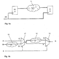
- FIGS. 1 a and 1 b illustrate the task of static timing analysis and the problem of false paths.
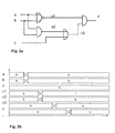
- FIGS. 2 a and 2 b show an example of X-valued timing simulation.
- FIG. 3 shows the longest paths found within the example of FIG. 2 a.
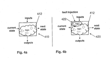
- FIGS. 4 a and 4 b show how timing exceptions are modelled according to the invention.
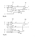
- FIGS. 5 a and 5 b , 5 c and 5 d show how representations of a logic circuit can be modified to model potential malfunction introduced by timing exceptions.
- FIGS. 6 a and 6 b show how malfunctions are introduced in a sequential context according to one embodiment of the invention.
- FIG. 7 shows an example of a sequential logic circuit.
- FIG. 8 a shows the logic of FIG. 7 in a combinational representation.
- FIG. 8 b shows a modified representation of the circuit of FIG. 8 a with introduced malfunctions.
- FIG. 9 shows a combinatorial representation of two time steps of the circuit of FIGS. 8 a and 8 b where a context dependent malfunction for a two cycle path is introduced.
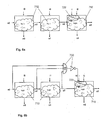
- FIG. 1 a shows a prototypical part of a sequential circuit with a first flip-flop (FF) 12 and as second FF 13 . Both of the FFs 12 , 13 are clocked by the same clock and a data input of second FF 13 depends on some combinational logic 11 driven by the first FF 12 . Static timing verification has to check (so called setup check) that after a first clock pulse arrives at the first FF 12 the data input of the second FF 13 will be stable before a second clock pulse arrives at the second FF 13 .
- setup check has to check (so called setup check) that after a first clock pulse arrives at the first FF 12 the data input of the second FF 13 will be stable before a second clock pulse arrives at the second FF 13 .
- This check is done by checking whether the length of a path from a clock input clk to the first FF 12 plus the length of the longest path through the combinational logic 11 is shorter than the length of a path from the clock input clk to the second FF 13 plus the intended clock period.
- FIG. 1 b illustrates a simple false path, demonstrating that the pure topological check done by static timing analysis may be too conservative.
- the combinational circuit of FIG. 1 b which comprises a first combinational logic 15 , a second combinational logic 16 , a first multiplexer 17 and a second multiplexer 18 , is part of the combinational logic 11 in FIG. 1 a , the longest path used for the setup time check will probably go through the first combinational logic 15 , the first multiplexer 17 , the second combinational logic 16 , and the multiplexer 18 (dotted line).
- FIGS. 2 a and 2 b illustrate X-valued timing simulation which serves as an operational model.
- This operational model can be used to illustrate the meaning of valid timing exception or a valid set of timing exceptions.
- X-valued timing simulation the value X is used for an undefined value. First all of the signals are undefined. At some time point, a defined value (0 or 1) is assigned to the inputs of the circuit. This value assignment is propagated through the circuit taking into account functionality and delay times of each of the gates in the circuit, e.g. the output of an AND gate with two inputs is determined after one of the inputs has become 0 or both of the inputs have become 1. Therefore in X-valued timing simulation the output of the AND gate becomes 1 at some specified delay after both of the inputs have become 1 and the output of the AND gate becomes 0 at some specified delay after the first input has become 0 (the other input may still be X).
- FIG. 2 b shows how an assignment of value 0 to the inputs propagates through the circuit given in FIG. 2 a assuming unit delay at each of the gates.
- Exact data arrival time can be computed for every one of the input assignments using X-valued timing simulation. Since the number of input assignments is exponential to the number of the inputs, it is not feasible to do this simulation for all input assignments (and all potential gate delays) in practice.
- X-valued simulation can be used as a reference model and it can be defined that a set of timing exceptions is valid if and only if for all gate delays the longest path found by static timing analysis (under given exceptions) is not shorter than data arrival time determined by X-valued simulation.
- FIGS. 4 a and 4 b give a general graphical representation of the embodiment of this invention.
- a sequential circuit 410 can always be presented as depicted in FIG. 4 a as a combinational logic 412 depending on inputs and current states as well as producing outputs and next states. Given a set of timing exceptions the sequential circuit 410 can be modified to obtain a fault modelling circuit 420 depicted in FIG. 4 b .
- the fault modelling circuit 420 in FIG. 4 b has some additional inputs and a fault injection logic 422 for fault injection.
- a set of timing exceptions related to the combinational logic 412 can be split into subclasses, so that for every subclass there is one new input which can be used to switch the potential fault introduced by this subclass of timing exceptions on and off.
- the fault modelling circuit 420 combined of the combinational logic 412 and the fault injection logic 422 is by construction functionally equivalent to the sequential circuit 410 and the combinational logic 412 of FIG. 4 a . If all of the fault injecting inputs are set to 1 the sequential circuit 410 and the fault modelling circuit 420 are functionally equivalent if and only if the whole set of timing exceptions is valid. If some fault injecting inputs are set to 1 the sequential circuit 410 the fault modelling circuit 420 are functionally equivalent if and only if the ensemble of the subclasses corresponding to the fault injecting inputs set to 1 forms a valid set of timing exceptions. Thus, by setting fault injection inputs selectively to 1 any combination of timing exceptions can be verified and invalid timing exceptions can be identified in a time efficient way.
- FIGS. 5 a to 5 c illustrate—using the example from FIG. 2 a —how a circuit of the form depicted in FIG. 4 a can be transformed to a fault modelling circuit 420 of the form depicted in FIG. 4 b .
- the transformation to the fault model is done in two steps: first some parts of the logic have to be duplicated, until every input can be uniquely associated to some (subclass of) timing exceptions or to the exception free part. In a second step a fault input fi and a switch are added for each timing exception subclass.
- FIG. 5 a reproduces FIG. 2 a .
- an additional output y is added. Assuming that a set containing the two false path exceptions (a,n 2 ,n 3 ,z) and (b,n 2 ,n 3 ,z) is given and in order to split these two false path exceptions into two subclasses, each subclass containing one single element, the logic of circuit of FIG. 5 a has to be duplicated to obtain the circuit illustrated in FIG. 5 b .
- an AND-gate 54 with inputs a and b and output n 2 is duplicated into a first AND-gate 541 with first inputs a′ and b′ and a first output n 2 ′ corresponding to a first output y and into a second AND-gate 542 with second inputs a′′ and b′′ and a second output n 2 ′′ corresponding to the branch of n 2 applied to a gate 56 .
- This new representation of the circuit has the property that every path starting at a′ or b′ is not contained in the set of timing exceptions, that every path starting at a′′ (in the example shown there is only one path) is contained in the first subclass of timing exceptions and every path starting at b′′ (in the example shown there is only one path) is contained in the second subclass.
- FIG. 5 d illustrates how a circuit can be constructed from FIG. 5 c , which has an input for every subclass of timing exceptions, which allows for analysing faulty behaviour for every combination of subclasses. Thereby a first multiplexer switch 641 and a second multiplexer switch 642 are introduced to inject fault into the signal a′ and b′, respectively.
- both of the inputs f 1 and f 2 in FIG. 5 d are set to 0, then the circuit of FIG. 5 d is functionally equivalent to that of the circuit that of FIG. 2 a by construction. If the input f 1 is set to 1 and the input f 2 is set to 0 then it is not obvious but it can be shown, e.g. using formal equivalence checking or property checking techniques, that the circuits of FIGS. 5 d and 2 a still are functionally equivalent. The same is true if the input f 1 is set to 0 and the input f 2 is set to 1. If the input f 1 is set to 1 and the input f 2 is set to 1 then the circuit of FIGS.
- 5 d and 2 a are not functionally equivalent any more, but there is an assignment to a′, b′ and c′ which makes a value X occur at output z in circuit of FIG. 5 d . From this analysis it can be concluded that a set of timing exceptions consisting of both false paths is invalid, but that the set of timing exception is valid if it has only one of these false paths as timing exception.
- FIGS. 6 a and 6 b show how a fault model of type shown in FIG. 4 b can be analyzed in a sequential context using the combinational representation of the sequential circuit given in FIG. 4 a .
- This representation can be used to build a combinational model of n sequential steps of the circuit 712 by n copies of 4 a where the next states of copy i are fed to the states of copy i+1.
- ff 0 , ff 1 , ff 2 , ff 3 denote one single signal in the state signals s 0 , s 1 , s 2 , s 3 respectively and further assuming that there is subclass of timing exceptions containing “3-cycle paths” starting all at the flip flop ff and going through the logic 712 , the introduction of a potential fault introduced by this subclass may be suppressed for those cases where the value of ff did not change for the last 3 cycles.
- Some switching logic 730 is added which switches off the fault from this subclass if and only if ff and thus signals ff 0 , ff 1 and ff 2 had the same value within the 3 last steps.
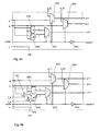
- FIG. 7 shows a detailed example of a sequential logic circuit or a section of a sequential logic circuit with storing elements a 810 , b 820 , c 880 , and mode 890 (whereby each of the storing elements a 810 , b 820 , c 880 may consist of one or more flip flops and mode is one single bit.).
- the mode 890 switches value between 0 and 1 e.g. by use of an inverter 895 .
- the storing element c 880 stores the sum or the product of the values of the storing element a 810 and the storing element b 820 .
- the storing element a 810 and the storing element b 820 keep their values or are updated according to signal a_in and signal b_in. It will be demonstrated how the invention can be used to show that a set of timing exceptions consisting of two 2-cycle paths (a,p,c) and (b,p,c) is valid.
- the representation of the circuit shown in FIG. 7 is transformed to a pure combinational representation (like in FIG. 4 a ) obtaining the circuit depicted in FIG. 8 a .
- the combinational representation of the circuit depicted in FIG. 8 a represents the same circuit and is therefore functionally identical to the representation of the circuit shown in FIG. 7 .
- This combinational representation of the circuit is then, according to the invention, transformed to a fault model (like in FIG. 4 b ) obtaining a modified representation of the circuit depicted in FIG. 8 b .
- the representation of the circuit depicted in FIG. 8 b is modified with an input for every subclass of timing exceptions, which allows for analysing faulty behaviour for every combination of subclasses.
- first multiplexer switch 941 and a second multiplexer switch 942 are introduced to inject fault values X into the signals a′ and b′ before they are respectively applied as signals a′′ and b′′ to multiplier 940 .
- Both the first multiplexer switch 941 and the second multiplexer switch 942 are individually controlled by fault injection inputs f 1 and f 2 , respectively.
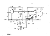
- FIGS. 8 a and 8 b From the circuits depicted in FIGS. 8 a and 8 b a fault model for two time steps can be constructed as explained with respect to FIG. 6 b .
- the resulting fault model can be seen in FIG. 9 .
- the faults injection is switched off by logic elements 1043 and 1044 , respectively, and the outputs a 1 ′′ and b 1 ′′ of 1041 and 1042 are set to the values of a 1 and b 1 , respectively.
- No X value is introduced to an input of a multiplier 1040 , therefore no X value is read at the output c 2 .
- mode 0 is 1, then mode 1 is 0 and a multiplexer 1070 switches to the result of an adder 1030 . Again no X value can be read at the output c 2 .
- circuits shown are illustrated by way of example only.
- the circuits shown may be regarded as simplified examples for easier understanding of the invention. Circuits usually applied in the field and within the invention will be much more complex than the circuits shown. It has to be noted that all the circuit shown can be a section or a part of a greater integrated circuit.
Abstract
Description
- The present application claims priority to and the benefit of the filing date of European Patent Application Serial No. EP 06 022 162.9 filed on Oct. 23, 2006, which is hereby incorporated by reference in its entirety.
- None.
- 1. Field of the Invention
- The present invention relates to the field of digital circuits. In particular, the present invention relates to the verification of digital circuits.
- 2. Brief Description of the Related Art
- Digital or logic circuits are implemented in almost any electronic device available today and offer the possibility of integrating an increasing number of functions and features into devices without raising production costs considerably. However, with the increasing number of features and functions, the number of circuit elements and thereby the complexity of the digital or logic circuits has increased. Consequently, the effort undertaken to design the digital or logic circuits has enormously increased.
- In usual design procedures an engineer or a team of engineers develops a design of the logic circuit or an assembly of the logic circuits that implements the desired functions. In order to represent or describe a design a number of description modes and methods have been developed describing a logic circuit at different levels. These description modes and methods include, for example, RTL or net list description.
- Once the design for the logic circuit has been developed and described according to the requirements of the desired application, a chip layout of the logic circuit has to be designed before the chip production process is started. It has become evident that mistakes or unforeseen circuitry may cause malfunctions in the chip which results in high costs for the correction of the design once the chip production process has started. Therefore, verification methods have been introduced in order to verify that the design of the chip layout fulfils all the requirements of the desired logic circuit. These verification methods may be applied before the production process or even during the design steps in order to find any faults in the design of the chip layout as soon as possible.
- The verification methods analyse the function and/or the layout of the design of the chip layout in order to simulate the function of the chip. Different types of the verification methods, i.e. timing verification or functional verification methods, are currently known in the art.
- The aim of static timing analysis is to verify that a logic circuit, in particular a digital circuit, satisfies its timing constraints, i.e. that the logic circuit will function correctly when run at an intended speed.
- It is state of the art in static timing analysis to check for potential setup (and hold) time violations by computing longest paths (with respect to gate and wire delays) through the logic circuit. It is well known that this check may be too conservative, because the check may find critical paths which cannot be activated while the chip is operating. This is due to the fact that static timing analysis performs a pure topological analysis of the logic circuit and does not take the functionality of the logic circuit into account. It is state of the art in static timing analysis to circumvent this problem by specifying so called timing exceptions. Timing exceptions are typically used for specifying paths to be false paths or to be multi-cycle paths. The timing exceptions are typically provided by the user of static timing analysis tools. The timing exceptions have the effect that those timing violations, which are specified to be exceptional, are simply ignored by the static timing analysis tool. It is evident that this procedure is error-prone. For example, static timing analysis may ignore relevant timing violations if the timing violation has been wrongly specified to be a timing exception, termed invalid timing exception which can lead to operational malfunction of the logic circuit. Timing violations that are correctly specified as timing exceptions are termed valid timing exception.
- Therefore, there is a need for an automated system which allows to check whether a set of given timing exceptions or timing violations is valid or to find a set of valid timing exceptions that is fast and reliable even with a large logic circuits and large numbers of timing violations.
- There are different published methods and available software tools which claim to solve this task at least partially. However, all of them suffer from different drawbacks. A large variety attacks the special case of false path exceptions. Most of them are trying to find a way to characterize a single path as false or true. It is well known, that these methods are either faulty, or too weak, or they need exact gate delay times. Only a few seem to be aware of the problem that a set of false path exceptions has to be analyzed as an entirety to decide whether it is valid or not.
- U.S. Pat. No. 5,638,290 describes a method for removing critical false paths during logic optimization based on a redundancy removal algorithm using essentially thee steps: starting a timing verification, searching for critical paths, extracting critical cones. This method has to be iteratively repeated for as long as a critical path is false.
- However, there is no method available to analyze different kinds of timing exceptions, e.g. multi cycle paths and false paths simultaneously.
- Further, there is a need for an automated system and a method for checking exceptions or violations, in particular timing exceptions, in a logic circuit that is fast, reliable and applicable to complex logic circuits.
- There is also a need for a method and a system for checking exceptions in a logic circuit that can be implemented in standard verification procedures.
- It is therefore an object of the present invention to provide a system for verifying exceptions that allows the automated determination whether a set of exceptions is of influence for the proper function of the chip or not.
- These and other objects of the present invention are solved by a method for verifying one or more exceptions in a logic circuit comprising: a first step of providing an initial representation of a logic circuit, a second step of indicating at least one exception for the logic circuit, a third step of introducing one or more potential malfunctions of the logic circuit related to the one or more timing exceptions into the initial representation of the logic circuit to produce a modified representation of the logic circuit, a fourth step of determining whether functional behaviour of the modified representation of the logic circuit differs from functional behaviour of the initial representation of the logic circuit, and a fifth step of reporting a result relating to the difference in the functional behaviour of the modified representation of the logic circuit from the functional behaviour of the initial representation of the logic circuit.
- The method according to the invention verifies a set of exceptions in an efficient and automated way. Using the method of the invention, an exception that is verified may be considered a valid exception and an exception that can not be verified may be considered invalid.
- The first representation of the logic circuit may thereby be in a description format known in the art such as an RTL or net list format, but other representations or description formats for a logic circuit may be used.
- In a preferred embodiment of the invention the one or more exceptions are timing exceptions. The exceptions may also be any timing violation in the logic circuit. Thus the invention may be advantageously applied for the verification of timing exceptions of a logic circuit. Alternatively, the one or more exceptions are clock domain crossings or similar.
- Timing exceptions which have been verified to be valid may be safely used by known procedures such as static timing analysis (STA) tools, place and route tools, or other tools.
- According to the invention, an exception or a timing exception may be verified by introducing a potential malfunction into the representation of the logic circuits. In particular, the potential malfunction may be introduced by modifying the representation of the logic circuit, especially by duplicating shared parts of the logic and adding switches and new inputs which allow conditional fault induction to one of the duplicate logics while the other of the duplicate logics maintains its original functionality. It can be checked or verified, whether inducing a fault by switching on or off of the malfunction of the logic circuit in the modified representation has an influence on the function of the logic circuit, i.e. whether the functional behaviour of the logic circuit described by the modified representation differs from the function of the logic circuit described by the unmodified description.
- The exception may also be verified for a particular use of the logic circuit. In general, the importance and/or validity of an exception may be different for different uses of the logic circuit. Thus an exception may be true in some instances while the exception is false in others.
- In a preferred embodiment of the present invention, the malfunctions are caused by the exceptions.
- In another preferred embodiment, the result in the fifth step indicates whether each of the one or more exceptions is acceptable for the initial representation of the logic circuit or reporting a sequence of events showing a faulty behaviour of the initial representation of the logic circuit under and/or for the indicated exception.
- In a preferred embodiment at least a section of the circuit is represented by a directed acyclic graph comprising nodes and edges, and defining paths through the nodes, wherein each path runs from an input node to an output node.
- In a further preferred embodiment the one or more timing exception defines a set of paths, the set comprising one or more timing exception paths. The one or more timing exception paths may comprise false paths or multi cycle paths but can be any type of path running between two nodes. The two nodes may thereby be input and/or output nodes of the logic circuit, but can be in principle any node of the represented circuit. A timing exception may thus be either a false path exception or a multi cycle path exception.
- In a further preferred embodiment the third step further comprises duplicating the nodes and/or edges in the representation of the logic circuit until every input node of the modified representation of the logic circuit is either a start point of one of the timing exceptions paths or a start point of one of a non-timing exception paths. In this way, the initial representation of the logic circuit is modified into a modified representation that can be easily separated into at least two parts. One part of the modified representation does not contain any path specified as timing exception. Another part of the modified representation contains solely paths specified as timing exception.
- In another embodiment of the invention the functional behaviour of the initial representation of the logic circuit and/or the modified representation of the logic circuit is defined in terms of 3-valued (X-valued) simulation comprising gate delay times and net delay times.
- In yet a further embodiment of the present invention the method comprises one or more multiplexer switches to introduce the malfunction into the representation of the logic circuit. Multiplexer switches may be integrated into the modified representation of the logic circuit in order to switch on and/or off introduction of fault values along paths or sections of the logic circuit for determining the function of the logic circuit, i.e. whether the timing exceptions modify the functional behaviour of the logic circuit. Using a plurality of multiplexer switches introduced at different places in the representation of the logic circuit allows the verification of a plurality of combinations of timing exceptions.
- In another preferred embodiment of the invention a plurality of initial representations of the logic circuit and modified representation of the logic circuit are connected sequentially to represent a multiple cycle simulation. The timing exception may herein comprise multi-cycle paths.
- In a further embodiment of the invention, a static 3-valued model is defined and at least one formal verification method is used to determine whether the functional behaviour of the modified representation of the logic circuit differs from the functional behaviour of the initial representation of the logic circuit.
- In yet a further embodiment the timing exceptions are grouped in subcategories of timing exceptions, one subcategory of timing exceptions for multi-cycle paths of same cycle length and identical start point, and/or one or more subcategories containing false paths, so that a static model for potential sequential malfunction can be constructed.
- Thereby, the third step may further comprise duplicating the nodes and/or edges in the representation of the logic circuit until every input node of the modified representation of the logic circuit is either a start point of a false path, a start point of one subcategory of multi-cycle path or a start point of non timing exceptions paths.
- In all the embodiments of the invention the logic circuit represented may be a section of an integrated circuit. A complete integrated circuit can also be represented.
- The invention is also advantageously applied in a method for verifying logic circuits comprising the steps of generating a representation of a logic circuit, identifying timing exception for the logic circuits verifying the timing exceptions using the method according to any of the embodiments of the invention discussed above.
- The method may also be used in a computer program product that allows for execution on a computer.
- In a preferred embodiment, the present invention is a method for verifying one or more exceptions in a logic circuit, the method comprising the steps of providing an initial representation of a logic circuit, indicating at least one exception for the logic circuit, introducing one or more potential malfunctions of the logic circuit related to the one or more exceptions into the representation of the logic circuit to produce a modified representation of the logic circuit, determining whether functional behaviour of the modified representation of the logic circuit differs from functional behaviour of the first representation of the logic circuit, and reporting a result relating to the difference in the functional behaviour of the modified representation of the logic circuit from the functional behaviour of the initial representation of the logic circuit. The one or more exceptions may be, for example, timing exceptions. The malfunction may be caused by the indicated one or more exceptions. Further, in one embodiment, the result in the reporting step indicates whether each of the one or more exceptions is acceptable for the initial representation of the logic circuit or reporting a sequence of events showing a faulty behaviour of the initial representation of the logic circuit for the indicated exception. Further, in one embodiment, at least a section of the circuit may be represented by a directed acyclic graph comprising nodes and edges, and defining paths through the nodes, wherein each path runs from an input node to an output node. In another embodiment, the one or more exceptions are timing exceptions and the one or more timing exception defines a set of paths, the set comprising one or more timing exception path. The one or more timing exception paths may comprise false paths. In another embodiment, introducing step further comprises duplicating the nodes and/or edges in the representation of the logic circuit until every input node of the modified representation of the logic circuit is either a start point of timing exceptions paths or a start point of non timing exceptions paths. In still another embodiment, the functional behaviour of the initial representation of the logic circuit and/or the modified representation of the logic circuit is defined in terms of 3-valued (X-valued) simulation comprising gate delay times and net delay times. In other embodiments, the method further comprises one or more multiplexer switches to introduce the malfunction into the representation of the logic circuit. Still further, a plurality of initial representations of the logic circuit and modified representation of the logic circuit may be connected sequentially to represent a multiple cycle simulation. The one or more timing exception may define a set of paths, the set comprising one or more timing exception path and wherein the timing exception paths comprise multi-cycle paths. Further, a static 3-valued model may be defined and at least one formal verification method is used to determine whether the functional behaviour of the modified representation of the logic circuit differs from the functional behaviour of the initial representation of the logic circuit. In another embodiment, the one or more exceptions are timing exceptions and the one or more timing exception defines a set of paths, the set comprising one or more timing exception path and the timing exceptions are grouped in subcategories of timing exceptions, one subcategory for every cycle length of multi-cycle path and/or for false path, so that a static model for potential sequential malfunction can be simulated. The introducing step may further comprise duplicating the nodes and/or edges in the representation of the logic circuit until every input node of the modified representation of the logic circuit is either a start point of a false path, a start point of one subcategory of multi-cycle path or a start point of non timing exceptions paths. The logic circuit may be a section of an integrated circuit.
- In another embodiment, the present invention is a method for verifying logic circuits comprising the steps of generating a representation of a logic circuit, identifying timing exception for the logic circuits and verifying the timing exceptions. The verifying step comprises the steps of a first step of providing an initial representation of a logic circuit, a second step of indicating at least one exception for the logic circuit, a third step of introducing one or more potential malfunctions of the logic circuit related to the one or more exceptions into the representation of the logic circuit to produce a modified representation of the logic circuit, a fourth step of determining whether functional behaviour of the modified representation of the logic circuit differs from functional behaviour of the first representation of the logic circuit, and a fifth step of reporting a result relating to the difference in the functional behaviour of the modified representation of the logic circuit from the functional behaviour of the initial representation of the logic circuit.
- In another embodiment, the present invention is a computer program product for verifying logic circuits applying a method comprising the steps of a first step of providing an initial representation of a logic circuit, a second step of indicating at least one exception for the logic circuit, a third step of introducing one or more potential malfunctions of the logic circuit related to the one or more exceptions into the representation of the logic circuit to produce a modified representation of the logic circuit, a fourth step of determining whether functional behaviour of the modified representation of the logic circuit differs from functional behaviour of the first representation of the logic circuit, and a fifth step of reporting a result relating to the difference in the functional behaviour of the modified representation of the logic circuit from the functional behaviour of the initial representation of the logic circuit.
- Still other aspects, features, and advantages of the present invention are readily apparent from the following detailed description, simply by illustrating a preferable embodiments and implementations. The present invention is also capable of other and different embodiments and its several details can be modified in various obvious respects, all without departing from the spirit and scope of the present invention. Accordingly, the drawings and descriptions are to be regarded as illustrative in nature, and not as restrictive. Additional objects and advantages of the invention will be set forth in part in the description which follows and in part will be obvious from the description, or may be learned by practice of the invention.
- For a more complete understanding of the present invention and the advantages thereof, reference is now made to the following description and the accompanying drawings, in which:
-
FIGS. 1 a and 1 b illustrate the task of static timing analysis and the problem of false paths. -
FIGS. 2 a and 2 b show an example of X-valued timing simulation. -
FIG. 3 shows the longest paths found within the example ofFIG. 2 a. -
FIGS. 4 a and 4 b show how timing exceptions are modelled according to the invention. -
FIGS. 5 a and 5 b, 5 c and 5 d show how representations of a logic circuit can be modified to model potential malfunction introduced by timing exceptions. -
FIGS. 6 a and 6 b show how malfunctions are introduced in a sequential context according to one embodiment of the invention. -
FIG. 7 shows an example of a sequential logic circuit. -
FIG. 8 a shows the logic ofFIG. 7 in a combinational representation. -
FIG. 8 b shows a modified representation of the circuit ofFIG. 8 a with introduced malfunctions. -
FIG. 9 shows a combinatorial representation of two time steps of the circuit ofFIGS. 8 a and 8 b where a context dependent malfunction for a two cycle path is introduced. -
FIG. 1 a shows a prototypical part of a sequential circuit with a first flip-flop (FF) 12 and assecond FF 13. Both of theFFs second FF 13 depends on somecombinational logic 11 driven by thefirst FF 12. Static timing verification has to check (so called setup check) that after a first clock pulse arrives at thefirst FF 12 the data input of thesecond FF 13 will be stable before a second clock pulse arrives at the second FF13. This check is done by checking whether the length of a path from a clock input clk to thefirst FF 12 plus the length of the longest path through thecombinational logic 11 is shorter than the length of a path from the clock input clk to thesecond FF 13 plus the intended clock period. -
FIG. 1 b illustrates a simple false path, demonstrating that the pure topological check done by static timing analysis may be too conservative. Assuming that the combinational circuit ofFIG. 1 b, which comprises afirst combinational logic 15, asecond combinational logic 16, afirst multiplexer 17 and asecond multiplexer 18, is part of thecombinational logic 11 inFIG. 1 a, the longest path used for the setup time check will probably go through thefirst combinational logic 15, thefirst multiplexer 17, thesecond combinational logic 16, and the multiplexer 18 (dotted line). As thefirst multiplexer 17 and thesecond multiplexer 18 are controlled by a same signal S it is not possible that this longest path is causing the data arrival time at the output G of thesecond multiplexer 18 and therefore the data arrival time at the data input of thesecond FF 13 ofFIG. 1 a. It will therefore be safe to simply ignore all such paths in the setup time check for thesecond FF 13. A user of static timing analysis may therefore want to specify these paths as a valid false path timing exception. -
FIGS. 2 a and 2 b illustrate X-valued timing simulation which serves as an operational model. This operational model can be used to illustrate the meaning of valid timing exception or a valid set of timing exceptions. In X-valued timing simulation the value X is used for an undefined value. First all of the signals are undefined. At some time point, a defined value (0 or 1) is assigned to the inputs of the circuit. This value assignment is propagated through the circuit taking into account functionality and delay times of each of the gates in the circuit, e.g. the output of an AND gate with two inputs is determined after one of the inputs has become 0 or both of the inputs have become 1. Therefore in X-valued timing simulation the output of the AND gate becomes 1 at some specified delay after both of the inputs have become 1 and the output of the AND gate becomes 0 at some specified delay after the first input has become 0 (the other input may still be X). -
FIG. 2 b shows how an assignment ofvalue 0 to the inputs propagates through the circuit given inFIG. 2 a assuming unit delay at each of the gates. Exact data arrival time can be computed for every one of the input assignments using X-valued timing simulation. Since the number of input assignments is exponential to the number of the inputs, it is not feasible to do this simulation for all input assignments (and all potential gate delays) in practice. However, X-valued simulation can be used as a reference model and it can be defined that a set of timing exceptions is valid if and only if for all gate delays the longest path found by static timing analysis (under given exceptions) is not shorter than data arrival time determined by X-valued simulation. - If a unit delay for every gate in the circuit given in
FIG. 2 a is not assumed, the two paths (a,n2,n3,z) and (b,n2,n3,z) (shown as dotted and dashed line inFIG. 3 , respectively) might have different lengths. X-valued simulation will demonstrate that the data arrival time at z will never be determined by the length of the longer one of these two paths but might be determined by the length of the shorter one. Therefore specifying solely (a,n2,n3,z) as a false path is a valid set of timing exceptions, and specifying solely (b,n2,n3,z) is as well a valid set of timing exceptions. However, specifying both of the paths as false paths is not a valid set of timing exceptions. -
FIGS. 4 a and 4 b give a general graphical representation of the embodiment of this invention. Asequential circuit 410 can always be presented as depicted inFIG. 4 a as acombinational logic 412 depending on inputs and current states as well as producing outputs and next states. Given a set of timing exceptions thesequential circuit 410 can be modified to obtain afault modelling circuit 420 depicted inFIG. 4 b. Thefault modelling circuit 420 inFIG. 4 b has some additional inputs and afault injection logic 422 for fault injection. A set of timing exceptions related to thecombinational logic 412 can be split into subclasses, so that for every subclass there is one new input which can be used to switch the potential fault introduced by this subclass of timing exceptions on and off. If all of the new fault injecting inputs of thefault injection logic 422 inFIG. 4 b are set to 0, thefault modelling circuit 420 combined of thecombinational logic 412 and thefault injection logic 422 is by construction functionally equivalent to thesequential circuit 410 and thecombinational logic 412 ofFIG. 4 a. If all of the fault injecting inputs are set to 1 thesequential circuit 410 and thefault modelling circuit 420 are functionally equivalent if and only if the whole set of timing exceptions is valid. If some fault injecting inputs are set to 1 thesequential circuit 410 thefault modelling circuit 420 are functionally equivalent if and only if the ensemble of the subclasses corresponding to the fault injecting inputs set to 1 forms a valid set of timing exceptions. Thus, by setting fault injection inputs selectively to 1 any combination of timing exceptions can be verified and invalid timing exceptions can be identified in a time efficient way. -
FIGS. 5 a to 5 c illustrate—using the example fromFIG. 2 a—how a circuit of the form depicted inFIG. 4 a can be transformed to afault modelling circuit 420 of the form depicted inFIG. 4 b. The transformation to the fault model is done in two steps: first some parts of the logic have to be duplicated, until every input can be uniquely associated to some (subclass of) timing exceptions or to the exception free part. In a second step a fault input fi and a switch are added for each timing exception subclass. -
FIG. 5 a reproducesFIG. 2 a. To illustrate the problem of duplicating logic an additional output y is added. Assuming that a set containing the two false path exceptions (a,n2,n3,z) and (b,n2,n3,z) is given and in order to split these two false path exceptions into two subclasses, each subclass containing one single element, the logic of circuit ofFIG. 5 a has to be duplicated to obtain the circuit illustrated inFIG. 5 b. In the particular case shown, an AND-gate 54 with inputs a and b and output n2 is duplicated into a first AND-gate 541 with first inputs a′ and b′ and a first output n2′ corresponding to a first output y and into a second AND-gate 542 with second inputs a″ and b″ and a second output n2″ corresponding to the branch of n2 applied to agate 56. This new representation of the circuit has the property that every path starting at a′ or b′ is not contained in the set of timing exceptions, that every path starting at a″ (in the example shown there is only one path) is contained in the first subclass of timing exceptions and every path starting at b″ (in the example shown there is only one path) is contained in the second subclass. Under the assumption a′=a″ and b′=b″ the circuits 5 a and 5 b are functionally equivalent by construction. - Without the output y, less duplication of gates would be necessary. The AND
gate 541 could be skipped and the circuit depicted inFIG. 5 c is obtained.FIG. 5 d illustrates how a circuit can be constructed fromFIG. 5 c, which has an input for every subclass of timing exceptions, which allows for analysing faulty behaviour for every combination of subclasses. Thereby afirst multiplexer switch 641 and asecond multiplexer switch 642 are introduced to inject fault into the signal a′ and b′, respectively. - If both of the inputs f1 and f2 in
FIG. 5 d are set to 0, then the circuit ofFIG. 5 d is functionally equivalent to that of the circuit that ofFIG. 2 a by construction. If the input f1 is set to 1 and the input f2 is set to 0 then it is not obvious but it can be shown, e.g. using formal equivalence checking or property checking techniques, that the circuits ofFIGS. 5 d and 2 a still are functionally equivalent. The same is true if the input f1 is set to 0 and the input f2 is set to 1. If the input f1 is set to 1 and the input f2 is set to 1 then the circuit ofFIGS. 5 d and 2 a are not functionally equivalent any more, but there is an assignment to a′, b′ and c′ which makes a value X occur at output z in circuit ofFIG. 5 d. From this analysis it can be concluded that a set of timing exceptions consisting of both false paths is invalid, but that the set of timing exception is valid if it has only one of these false paths as timing exception. -
FIGS. 6 a and 6 b show how a fault model of type shown inFIG. 4 b can be analyzed in a sequential context using the combinational representation of the sequential circuit given inFIG. 4 a. This representation can be used to build a combinational model of n sequential steps of thecircuit 712 by n copies of 4 a where the next states of copy i are fed to the states of copy i+1. InFIG. 6 a a model for n=3 is shown where in the third step a fault model as explained with respect toFIG. 6 b and indicated asfault inducing logic 722 inFIG. 6 a is introduced. This has the advantage that arbitrary assignments to s2 are not allowed when checking for potential X values at s3 or o2, but only those assignments to s2 are allowed, which can occur in the given sequential context. This sequential analysis can be further improved if the set of timing exceptions contains multi cycle paths. Assuming that the circuit contains a flip flop ff and therefore ff0, ff1, ff2, ff3 denote one single signal in the state signals s0, s1, s2, s3 respectively and further assuming that there is subclass of timing exceptions containing “3-cycle paths” starting all at the flip flop ff and going through thelogic 712, the introduction of a potential fault introduced by this subclass may be suppressed for those cases where the value of ff did not change for the last 3 cycles.FIG. 6 b demonstrates how this can be modelled: Some switchinglogic 730 is added which switches off the fault from this subclass if and only if ff and thus signals ff0, ff1 and ff2 had the same value within the 3 last steps. -
FIG. 7 shows a detailed example of a sequential logic circuit or a section of a sequential logic circuit with storing elements a 810,b 820,c 880, and mode 890 (whereby each of the storing elements a 810,b 820,c 880 may consist of one or more flip flops and mode is one single bit.). In every time step themode 890 switches value between 0 and 1 e.g. by use of aninverter 895. Depending on the current value ofmode 890, the storingelement c 880 stores the sum or the product of the values of the storing element a 810 and the storingelement b 820. Depending on the current value ofmode 890, the storing element a 810 and the storingelement b 820 keep their values or are updated according to signal a_in and signal b_in. It will be demonstrated how the invention can be used to show that a set of timing exceptions consisting of two 2-cycle paths (a,p,c) and (b,p,c) is valid. - First, the representation of the circuit shown in
FIG. 7 is transformed to a pure combinational representation (like inFIG. 4 a) obtaining the circuit depicted inFIG. 8 a. The combinational representation of the circuit depicted inFIG. 8 a represents the same circuit and is therefore functionally identical to the representation of the circuit shown inFIG. 7 . This combinational representation of the circuit is then, according to the invention, transformed to a fault model (like inFIG. 4 b) obtaining a modified representation of the circuit depicted inFIG. 8 b. The representation of the circuit depicted inFIG. 8 b is modified with an input for every subclass of timing exceptions, which allows for analysing faulty behaviour for every combination of subclasses. Thereby afirst multiplexer switch 941 and asecond multiplexer switch 942 are introduced to inject fault values X into the signals a′ and b′ before they are respectively applied as signals a″ and b″ tomultiplier 940. Both thefirst multiplexer switch 941 and thesecond multiplexer switch 942 are individually controlled by fault injection inputs f1 and f2, respectively. - If both of the fault injection inputs f1 and f2 in
FIG. 8 b are set to 0, than the modified circuit ofFIG. 8 b is functionally equivalent to that of the circuit ofFIG. 8 a by construction. - From the circuits depicted in
FIGS. 8 a and 8 b a fault model for two time steps can be constructed as explained with respect toFIG. 6 b. The resulting fault model can be seen inFIG. 9 . InFIG. 9 all logic which is not relevant to analyze the value at an output c2 is left out. It is easy to see that the fault value X can never occur at the output c2 in the circuit ofFIG. 9 . Therefore the fault model is functionally equivalent to the fault free model and as a result the modelled timing exceptions are valid. Only two cases have to be distinguished in order to see that the values of signal c2 can never become X: mode0=0 and mode0=1. If mode0 is 0 then themultiplexers logic elements multiplier 1040, therefore no X value is read at the output c2. On the other hand if mode0 is 1, then mode1 is 0 and amultiplexer 1070 switches to the result of anadder 1030. Again no X value can be read at the output c2. - It is obvious to a person skilled in the art that all circuits shown are illustrated by way of example only. The circuits shown may be regarded as simplified examples for easier understanding of the invention. Circuits usually applied in the field and within the invention will be much more complex than the circuits shown. It has to be noted that all the circuit shown can be a section or a part of a greater integrated circuit.
- The foregoing description of the preferred embodiment of the invention has been presented for purposes of illustration and description. It is not intended to be exhaustive or to limit the invention to the precise form disclosed, and modifications and variations are possible in light of the above teachings or may be acquired from practice of the invention. The embodiment was chosen and described in order to explain the principles of the invention and its practical application to enable one skilled in the art to utilize the invention in various embodiments as are suited to the particular use contemplated. It is intended that the scope of the invention be defined by the claims appended hereto, and their equivalents. The entirety of each of the aforementioned documents is incorporated by reference herein.
Claims (18)
Applications Claiming Priority (3)
| Application Number | Priority Date | Filing Date | Title |
|---|---|---|---|
| EP06022162A EP1916534B1 (en) | 2006-10-23 | 2006-10-23 | Verification and generation of timing exceptions |
| EP06022162.9 | 2006-10-23 | ||
| EP06022162 | 2006-10-23 |
Publications (2)
| Publication Number | Publication Date |
|---|---|
| US20080098271A1 true US20080098271A1 (en) | 2008-04-24 |
| US7818700B2 US7818700B2 (en) | 2010-10-19 |
Family
ID=38051555
Family Applications (1)
| Application Number | Title | Priority Date | Filing Date |
|---|---|---|---|
| US11/876,903 Active 2028-12-22 US7818700B2 (en) | 2006-10-23 | 2007-10-23 | System and method for verification and generation of timing exceptions |
Country Status (3)
| Country | Link |
|---|---|
| US (1) | US7818700B2 (en) |
| EP (1) | EP1916534B1 (en) |
| DE (1) | DE602006011177D1 (en) |
Cited By (9)
| Publication number | Priority date | Publication date | Assignee | Title |
|---|---|---|---|---|
| US20080059938A1 (en) * | 2006-09-05 | 2008-03-06 | Nec Corporation | Method of and system for designing semiconductor integrated circuit |
| US20080288904A1 (en) * | 2007-05-15 | 2008-11-20 | Atrenta, Inc. | Method for modeling and verifying timing exceptions |
| US20100064263A1 (en) * | 2008-09-08 | 2010-03-11 | Atrenta, Inc. | Method for compaction of timing exception paths |
| US8141015B1 (en) * | 2010-03-02 | 2012-03-20 | Altera Corporation | Reporting status of timing exceptions |
| US9208272B2 (en) * | 2010-08-13 | 2015-12-08 | Synopsys, Inc. | Apparatus and method thereof for hybrid timing exception verification of an integrated circuit design |
| CN108228373A (en) * | 2017-12-26 | 2018-06-29 | 中国信息通信研究院 | Failure of chip injects detection device and method |
| CN109672601A (en) * | 2019-01-15 | 2019-04-23 | 南京理工大学 | A kind of sub grade fault simulation system of rocket one |
| US10380301B1 (en) * | 2017-03-17 | 2019-08-13 | Cadence Design Systems, Inc. | Method for waveform based debugging for cover failures from formal verification |
| CN115062566A (en) * | 2022-06-21 | 2022-09-16 | 深圳国微芯科技有限公司 | Method for simplifying circuit containing X value, verification method and storage medium |
Families Citing this family (5)
| Publication number | Priority date | Publication date | Assignee | Title |
|---|---|---|---|---|
| US8479128B2 (en) * | 2011-03-03 | 2013-07-02 | Synopsys, Inc. | Technique for honoring multi-cycle path semantics in RTL simulation |
| EP2546767B1 (en) | 2011-07-11 | 2014-12-31 | OneSpin Solutions GmbH | Digital circuit verification monitor |
| US9032345B2 (en) | 2011-07-11 | 2015-05-12 | Onespin Solutions Gmbh | Digital circuit verification monitor |
| US8555220B2 (en) * | 2012-02-29 | 2013-10-08 | Umm Al-Qura University | Timing verification method for deterministic and stochastic networks and circuits |
| US10990736B1 (en) * | 2020-03-17 | 2021-04-27 | Xilinx, Inc. | Implementing a circuit design with re-convergence |
Citations (11)
| Publication number | Priority date | Publication date | Assignee | Title |
|---|---|---|---|---|
| US5638290A (en) * | 1995-04-06 | 1997-06-10 | Vlsi Technology, Inc. | Method for eliminating a false critical path in a logic circuit |
| US5648909A (en) * | 1992-06-12 | 1997-07-15 | Digital Equipment Corporation | Static timing verification in the presence of logically false paths |
| US5675728A (en) * | 1994-08-09 | 1997-10-07 | Sun Microsystems, Inc. | Apparatus and method identifying false timing paths in digital circuits |
| US5764525A (en) * | 1994-01-28 | 1998-06-09 | Vlsi Technology, Inc. | Method for improving the operation of a circuit through iterative substitutions and performance analyses of datapath cells |
| US20040078767A1 (en) * | 2001-06-08 | 2004-04-22 | Burks Timothy M. | Representing the design of a sub-module in a hierarchical integrated circuit design and analysis system |
| US20050246673A1 (en) * | 2004-04-30 | 2005-11-03 | International Business Machines Corporation | Method and system for performing static timing analysis on digital electronic circuits |
| US6964027B2 (en) * | 2003-04-16 | 2005-11-08 | Synopsys, Inc. | System and method for optimizing exceptions |
| US20080005710A1 (en) * | 2006-06-29 | 2008-01-03 | Lsi Logic Corporation | Automatic generation of timing constraints for the validation/signoff of test structures |
| US20080216040A1 (en) * | 2005-06-29 | 2008-09-04 | Geoffrey Mark Furnish | Incremental Relative Slack Timing Force Model |
| US7555689B2 (en) * | 2005-06-28 | 2009-06-30 | Dhiraj Goswami | Generating responses to patterns stimulating an electronic circuit with timing exception paths |
| US20090254874A1 (en) * | 2006-05-18 | 2009-10-08 | Subhasis Bose | Methods and systems for placement and routing |
Family Cites Families (1)
| Publication number | Priority date | Publication date | Assignee | Title |
|---|---|---|---|---|
| US6799287B1 (en) * | 2000-05-01 | 2004-09-28 | Hewlett-Packard Development Company, L.P. | Method and apparatus for verifying error correcting codes |
-
2006
- 2006-10-23 EP EP06022162A patent/EP1916534B1/en active Active
- 2006-10-23 DE DE602006011177T patent/DE602006011177D1/en active Active
-
2007
- 2007-10-23 US US11/876,903 patent/US7818700B2/en active Active
Patent Citations (15)
| Publication number | Priority date | Publication date | Assignee | Title |
|---|---|---|---|---|
| US5648909A (en) * | 1992-06-12 | 1997-07-15 | Digital Equipment Corporation | Static timing verification in the presence of logically false paths |
| US5764525A (en) * | 1994-01-28 | 1998-06-09 | Vlsi Technology, Inc. | Method for improving the operation of a circuit through iterative substitutions and performance analyses of datapath cells |
| US5675728A (en) * | 1994-08-09 | 1997-10-07 | Sun Microsystems, Inc. | Apparatus and method identifying false timing paths in digital circuits |
| US5638290A (en) * | 1995-04-06 | 1997-06-10 | Vlsi Technology, Inc. | Method for eliminating a false critical path in a logic circuit |
| US20040078767A1 (en) * | 2001-06-08 | 2004-04-22 | Burks Timothy M. | Representing the design of a sub-module in a hierarchical integrated circuit design and analysis system |
| US7103863B2 (en) * | 2001-06-08 | 2006-09-05 | Magma Design Automation, Inc. | Representing the design of a sub-module in a hierarchical integrated circuit design and analysis system |
| US6964027B2 (en) * | 2003-04-16 | 2005-11-08 | Synopsys, Inc. | System and method for optimizing exceptions |
| US20050246673A1 (en) * | 2004-04-30 | 2005-11-03 | International Business Machines Corporation | Method and system for performing static timing analysis on digital electronic circuits |
| US7555689B2 (en) * | 2005-06-28 | 2009-06-30 | Dhiraj Goswami | Generating responses to patterns stimulating an electronic circuit with timing exception paths |
| US20090327986A1 (en) * | 2005-06-28 | 2009-12-31 | Dhiraj Goswami | Generating responses to patterns stimulating an electronic circuit with timing exception paths |
| US20080216040A1 (en) * | 2005-06-29 | 2008-09-04 | Geoffrey Mark Furnish | Incremental Relative Slack Timing Force Model |
| US7669160B2 (en) * | 2005-06-29 | 2010-02-23 | Geoffrey Mark Furnish | Methods and systems for placement |
| US20090254874A1 (en) * | 2006-05-18 | 2009-10-08 | Subhasis Bose | Methods and systems for placement and routing |
| US20080005710A1 (en) * | 2006-06-29 | 2008-01-03 | Lsi Logic Corporation | Automatic generation of timing constraints for the validation/signoff of test structures |
| US7490307B2 (en) * | 2006-06-29 | 2009-02-10 | Lsi Corporation | Automatic generating of timing constraints for the validation/signoff of test structures |
Cited By (12)
| Publication number | Priority date | Publication date | Assignee | Title |
|---|---|---|---|---|
| US20080059938A1 (en) * | 2006-09-05 | 2008-03-06 | Nec Corporation | Method of and system for designing semiconductor integrated circuit |
| US7774730B2 (en) * | 2006-09-05 | 2010-08-10 | Nec Corporation | Method of and system for designing semiconductor integrated circuit |
| US20080288904A1 (en) * | 2007-05-15 | 2008-11-20 | Atrenta, Inc. | Method for modeling and verifying timing exceptions |
| US7650581B2 (en) * | 2007-05-15 | 2010-01-19 | Atrenta, Inc. | Method for modeling and verifying timing exceptions |
| US20100064263A1 (en) * | 2008-09-08 | 2010-03-11 | Atrenta, Inc. | Method for compaction of timing exception paths |
| US8042085B2 (en) * | 2008-09-08 | 2011-10-18 | Atrenta, Inc. | Method for compaction of timing exception paths |
| US8141015B1 (en) * | 2010-03-02 | 2012-03-20 | Altera Corporation | Reporting status of timing exceptions |
| US9208272B2 (en) * | 2010-08-13 | 2015-12-08 | Synopsys, Inc. | Apparatus and method thereof for hybrid timing exception verification of an integrated circuit design |
| US10380301B1 (en) * | 2017-03-17 | 2019-08-13 | Cadence Design Systems, Inc. | Method for waveform based debugging for cover failures from formal verification |
| CN108228373A (en) * | 2017-12-26 | 2018-06-29 | 中国信息通信研究院 | Failure of chip injects detection device and method |
| CN109672601A (en) * | 2019-01-15 | 2019-04-23 | 南京理工大学 | A kind of sub grade fault simulation system of rocket one |
| CN115062566A (en) * | 2022-06-21 | 2022-09-16 | 深圳国微芯科技有限公司 | Method for simplifying circuit containing X value, verification method and storage medium |
Also Published As
| Publication number | Publication date |
|---|---|
| EP1916534A1 (en) | 2008-04-30 |
| DE602006011177D1 (en) | 2010-01-28 |
| EP1916534B1 (en) | 2009-12-16 |
| US7818700B2 (en) | 2010-10-19 |
Similar Documents
| Publication | Publication Date | Title |
|---|---|---|
| US7818700B2 (en) | System and method for verification and generation of timing exceptions | |
| US7890901B2 (en) | Method and system for verifying the equivalence of digital circuits | |
| Foster et al. | Assertion-based design | |
| US7480610B2 (en) | Software state replay | |
| US7454728B2 (en) | Metastability injector for a circuit description | |
| US6321363B1 (en) | Incremental simulation using previous simulation results and knowledge of changes to simulation model to achieve fast simulation time | |
| US20030208730A1 (en) | Method for verifying properties of a circuit model | |
| US7822591B2 (en) | Logic circuit model conversion apparatus and method thereof; and logic circuit model conversion program | |
| US7254793B2 (en) | Latch modeling technique for formal verification | |
| US6748573B2 (en) | Apparatus and method for removing effects of phase abstraction from a phase abstracted trace | |
| JP5040758B2 (en) | Simulation apparatus, simulation method, and program | |
| US9053265B2 (en) | Generating test benches for pre-silicon validation of retimed complex IC designs against a reference design | |
| Savoj et al. | Sequential equivalence checking for clock-gated circuits | |
| US7080333B1 (en) | Verifying logic synthesizers | |
| US7328415B2 (en) | Modeling blocks of an integrated circuit for timing verification | |
| Chatterjee et al. | On resolution proofs for combinational equivalence | |
| KR101328263B1 (en) | Verification Method from Electronic System Level to Gate Level Using Systematic Progressive Refinement | |
| Kaiss et al. | Seqver: A sequential equivalence verifier for hardware designs | |
| JAIN | AUTOMATION OF RTL TO GDS II DESIGN FLOW USING SCRIPT’S METHODOLOGY | |
| Chang et al. | Automated methods for eliminating X bugs | |
| Shi et al. | Enhancing simulation accuracy through advanced hazard detection in asynchronous circuits | |
| JP2012160145A (en) | Logic simulation method and logic simulation apparatus | |
| KR20070108303A (en) | Verification method from electronic system level to gate level using systematic progressive refinement | |
| Kukimoto et al. | Delay characterization of combinational modules | |
| WO2014015185A1 (en) | Relative timing characterization |
Legal Events
| Date | Code | Title | Description |
|---|---|---|---|
| AS | Assignment |
Owner name: ONESPIN SOLUTIONS GMBH, GERMANY Free format text: ASSIGNMENT OF ASSIGNORS INTEREST;ASSIGNOR:MUELLER-BRAHMS, MARTIN, DR.;REEL/FRAME:022103/0930 Effective date: 20081216 |
|
| STCF | Information on status: patent grant |
Free format text: PATENTED CASE |
|
| FPAY | Fee payment |
Year of fee payment: 4 |
|
| MAFP | Maintenance fee payment |
Free format text: PAYMENT OF MAINTENANCE FEE, 8TH YR, SMALL ENTITY (ORIGINAL EVENT CODE: M2552) Year of fee payment: 8 |
|
| FEPP | Fee payment procedure |
Free format text: ENTITY STATUS SET TO UNDISCOUNTED (ORIGINAL EVENT CODE: BIG.); ENTITY STATUS OF PATENT OWNER: LARGE ENTITY |
|
| MAFP | Maintenance fee payment |
Free format text: PAYMENT OF MAINTENANCE FEE, 12TH YEAR, LARGE ENTITY (ORIGINAL EVENT CODE: M1553); ENTITY STATUS OF PATENT OWNER: LARGE ENTITY Year of fee payment: 12 |
|
| AS | Assignment |
Owner name: SIEMENS ELCETRONIC DESIGN AUTOMATION GMBH, GERMANY Free format text: MERGER AND CHANGE OF NAME;ASSIGNORS:ONESPIN SOLUTIONS GMBH;SIEMENS ELECTRONIC DESIGN AUTOMATION GMBH;REEL/FRAME:063581/0480 Effective date: 20220424 |
|
| AS | Assignment |
Owner name: SIEMENS ELECTRONIC DESIGN AUTOMATION GMBH, GERMANY Free format text: CORRECTIVE ASSIGNMENT TO CORRECT THE CLERICAL ERROR OF ELCETRONIC TO ELECTRONIC PREVIOUSLY RECORDED ON REEL 063581 FRAME 0480. ASSIGNOR(S) HEREBY CONFIRMS THE MERGER AND CHANGE OF NAME;ASSIGNOR:ONESPIN SOLUTIONS GMBH;REEL/FRAME:063889/0548 Effective date: 20220524 |