US20080098278A1 - Multiplier product generation based on encoded data from addressable location - Google Patents
Multiplier product generation based on encoded data from addressable location Download PDFInfo
- Publication number
- US20080098278A1 US20080098278A1 US11/540,346 US54034606A US2008098278A1 US 20080098278 A1 US20080098278 A1 US 20080098278A1 US 54034606 A US54034606 A US 54034606A US 2008098278 A1 US2008098278 A1 US 2008098278A1
- Authority
- US
- United States
- Prior art keywords
- circuitry
- encoded data
- data
- encoding
- encoded
- Prior art date
- Legal status (The legal status is an assumption and is not a legal conclusion. Google has not performed a legal analysis and makes no representation as to the accuracy of the status listed.)
- Granted
Links
- 238000000034 method Methods 0.000 claims description 5
- 238000001514 detection method Methods 0.000 claims description 4
- 238000010586 diagram Methods 0.000 description 11
- 238000004891 communication Methods 0.000 description 9
- 230000004044 response Effects 0.000 description 7
- 230000000295 complement effect Effects 0.000 description 5
- 230000017525 heat dissipation Effects 0.000 description 4
- 239000000446 fuel Substances 0.000 description 1
- 230000006870 function Effects 0.000 description 1
- 239000004973 liquid crystal related substance Substances 0.000 description 1
- 238000012986 modification Methods 0.000 description 1
- 230000004048 modification Effects 0.000 description 1
- 230000003068 static effect Effects 0.000 description 1
Images


Classifications
-
- G—PHYSICS
- G06—COMPUTING; CALCULATING OR COUNTING
- G06F—ELECTRIC DIGITAL DATA PROCESSING
- G06F7/00—Methods or arrangements for processing data by operating upon the order or content of the data handled
- G06F7/38—Methods or arrangements for performing computations using exclusively denominational number representation, e.g. using binary, ternary, decimal representation
- G06F7/48—Methods or arrangements for performing computations using exclusively denominational number representation, e.g. using binary, ternary, decimal representation using non-contact-making devices, e.g. tube, solid state device; using unspecified devices
- G06F7/52—Multiplying; Dividing
- G06F7/523—Multiplying only
-
- G—PHYSICS
- G11—INFORMATION STORAGE
- G11C—STATIC STORES
- G11C7/00—Arrangements for writing information into, or reading information out from, a digital store
- G11C7/10—Input/output [I/O] data interface arrangements, e.g. I/O data control circuits, I/O data buffers
- G11C7/1006—Data managing, e.g. manipulating data before writing or reading out, data bus switches or control circuits therefor
-
- G—PHYSICS
- G06—COMPUTING; CALCULATING OR COUNTING
- G06F—ELECTRIC DIGITAL DATA PROCESSING
- G06F7/00—Methods or arrangements for processing data by operating upon the order or content of the data handled
- G06F7/38—Methods or arrangements for performing computations using exclusively denominational number representation, e.g. using binary, ternary, decimal representation
- G06F7/48—Methods or arrangements for performing computations using exclusively denominational number representation, e.g. using binary, ternary, decimal representation using non-contact-making devices, e.g. tube, solid state device; using unspecified devices
- G06F7/52—Multiplying; Dividing
- G06F7/523—Multiplying only
- G06F7/533—Reduction of the number of iteration steps or stages, e.g. using the Booth algorithm, log-sum, odd-even
- G06F7/5332—Reduction of the number of iteration steps or stages, e.g. using the Booth algorithm, log-sum, odd-even by skipping over strings of zeroes or ones, e.g. using the Booth Algorithm
-
- G—PHYSICS
- G06—COMPUTING; CALCULATING OR COUNTING
- G06F—ELECTRIC DIGITAL DATA PROCESSING
- G06F7/00—Methods or arrangements for processing data by operating upon the order or content of the data handled
- G06F7/38—Methods or arrangements for performing computations using exclusively denominational number representation, e.g. using binary, ternary, decimal representation
- G06F7/48—Methods or arrangements for performing computations using exclusively denominational number representation, e.g. using binary, ternary, decimal representation using non-contact-making devices, e.g. tube, solid state device; using unspecified devices
- G06F7/52—Multiplying; Dividing
- G06F7/523—Multiplying only
- G06F7/533—Reduction of the number of iteration steps or stages, e.g. using the Booth algorithm, log-sum, odd-even
- G06F7/5334—Reduction of the number of iteration steps or stages, e.g. using the Booth algorithm, log-sum, odd-even by using multiple bit scanning, i.e. by decoding groups of successive multiplier bits in order to select an appropriate precalculated multiple of the multiplicand as a partial product
-
- G—PHYSICS
- G06—COMPUTING; CALCULATING OR COUNTING
- G06F—ELECTRIC DIGITAL DATA PROCESSING
- G06F7/00—Methods or arrangements for processing data by operating upon the order or content of the data handled
- G06F7/74—Selecting or encoding within a word the position of one or more bits having a specified value, e.g. most or least significant one or zero detection, priority encoders
Definitions
- Embodiments described herein generally relate to multipliers.
- a processor can have a multiplier circuit to help speed the generation of products of numbers.
- a processor can use a multiplier circuit, for example, to help speed performance of digital signal processing (DSP) applications such as, for example, finite impulse response (FIR) filters, infinite impulse response (IIR) filters, discrete cosine transforms (DCTs), and/or fast Fourier transforms (FFTs).
- DSP digital signal processing
- FIR finite impulse response
- IIR infinite impulse response
- DCTs discrete cosine transforms
- FFTs fast Fourier transforms
- a processor can have parallel clusters of multiplier, multiply-add, and/or multiply-accumulate circuits to help speed performance of complex filter operations, for example.
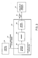
- FIG. 1 illustrates, for one embodiment, a block diagram of circuitry to generate a product based at least in part on encoded data from an addressable location;
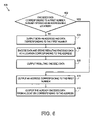
- FIG. 2 illustrates, for one embodiment, a flow diagram to generate a product based at least in part on encoded data from an addressable location
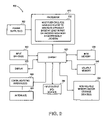
- FIG. 3 illustrates, for one embodiment, a block diagram of circuitry to output encoded data from an addressable location
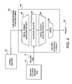
- FIG. 4 illustrates, for one embodiment, a block diagram of circuitry to generate a product based at least in part on encoded data corresponding to a first number and data corresponding to a second number;
- FIG. 5 illustrates, for one embodiment, a block diagram of circuitry to encode data and store encoded data at an addressable location
- FIG. 6 illustrates, for one embodiment, a flow diagram to output encoded data
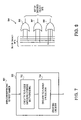
- FIG. 7 illustrates, for one embodiment, encoding circuitry for the block diagram of FIG. 5 ;
- FIG. 8 illustrates, for one embodiment, circuitry to perform modified leading zeroes detection (LZD) for the block diagram of FIG. 7 ;
- FIG. 9 illustrates, for one embodiment, a block diagram of an example system comprising a processor having circuitry to generate a product based at least in part on encoded data from an addressable location.
- FIG. 1 illustrates circuitry 100 to generate a product based at least in part on encoded data from an addressable location.
- Circuitry 100 for one embodiment may include circuitry 110 to output encoded data 111 from an addressable location based at least in part on an address 101 corresponding to a first number and circuitry 140 to generate a product 103 based at least in part on encoded data 111 and on data 102 corresponding to a second number.
- Encoded data 111 for one embodiment may be based at least in part on data that corresponds to the first number and that is encoded for partial product reduction.
- Circuitry 140 for one embodiment may generate a product of the first number and the second number.
- the first number may be a multiplier and the second number may be a multiplicand.
- the first number may be a multiplicand and the second number may be a multiplier.
- Circuitry 110 for one embodiment may be used to output encoded data 111 from an addressable location based at least in part on an address 101 corresponding to the first number to help reduce or avoid having to encode the same data repeatedly for partial product reduction. Circuitry 110 for one embodiment may be used to output encoded data to help speed performance of product generation. Circuitry 110 for one embodiment may be used to output encoded data to help reduce power consumption and/or heat dissipation. Circuitry 110 for one embodiment may be used to help speed performance and/or to help reduce power consumption and/or heat dissipation particularly where circuitry 110 is used to output encoded data 111 for a multiplier that is a constant and that is to be repeatedly multiplied with different multiplicands.
- FIG. 2 illustrates, for one embodiment, a flow diagram 200 to generate a product based at least in part on encoded data from an addressable location.
- circuitry 110 may output encoded data 111 from an addressable location based at least in part on address 101 corresponding to the first number.
- circuitry 140 may generate product 103 based at least in part on encoded data 111 and on data 102 corresponding to the second number.
- Encoded data 111 may correspond to a first number of any suitable bit-length, may be based at least in part on data that is encoded for partial product reduction in any suitable manner, and may have any suitable size. Encoded data 111 for one embodiment may correspond, for example, to a 16-bit first number. Encoded data 111 for one embodiment may include any suitable number of sets of any suitable number of select bits for a first number of any suitable bit-length.
- Encoded data 111 for one embodiment may be based at least in part on data that is encoded using Booth encoding or modified Booth encoding, such as radix-4 Booth (or modified Booth) encoding for example.
- Encoded data 111 for one embodiment may be the encoded data resulting from Booth encoding or modified Booth encoding of data corresponding to the first number.
- Encoded data 111 for one embodiment may be 48 bits in length, that is eight sets of six select bits, for a 16-bit number encoded using radix-4 Booth (or modified Booth) encoding.
- Encoded data 111 for one embodiment may be encoded data resulting from further encoding of already encoded data. Such further encoding for one embodiment may be used, for example, to help compress encoded data.
- Encoded data 111 for one embodiment may be the encoded data resulting from further encoding of already encoded data using leading zeroes detection (LZD) or modified LZD.
- Encoded data 111 for one embodiment may be encoded data resulting from Booth encoding or modified Booth encoding of data corresponding to the first number and further encoding of such encoded data using LZD or modified LZD.
- LZD or modified LZD encoding may be used to encode the eight sets of six select bits into eight sets of three encoded select bits for a total of 24 bits for encoded data 111 .
- Circuitry 110 may be coupled to receive address 101 of any suitable bit-length from any suitable source. Circuitry 110 for one embodiment, as illustrated in FIG. 1 , may be coupled to receive address 101 from control circuitry 130 .
- Control circuitry 130 may comprise any suitable circuitry to control output of address 101 to circuitry 110 in any suitable manner.
- Control circuitry 130 for one embodiment may store address 101 in one or more registers.
- Control circuitry 130 for one embodiment may output address 101 to circuitry 110 in response to data corresponding to the first number.
- Control circuitry 130 for one embodiment may convert data corresponding to the first number to address 101 .
- Circuitry 140 may be coupled to receive data 102 of any suitable bit-length from any suitable source. Circuitry 140 for one embodiment, as illustrated in FIG. 1 , may be coupled to receive data 102 from control circuitry 130 . Control circuitry 130 may comprise any suitable circuitry to control output of data 102 to circuitry 140 in any suitable manner. Control circuitry 130 for one embodiment may store data 102 in one or more registers.
- Control circuitry 130 for one embodiment may output data 102 to circuitry 140 as control circuitry 130 outputs address 101 to circuitry 110 .
- Control circuitry 130 for one embodiment may output address 101 and data 102 so as to be available on the same clock edge.
- Control circuitry 130 for one embodiment may include programmable logic to output address 101 and/or data 102 .
- Control circuitry 130 for one embodiment may output address 101 and/or data 102 in response to an instruction in order to execute the instruction.
- Circuitry 110 may include any suitable circuitry to output encoded data 111 from an addressable location in any suitable manner.
- Circuitry 110 for one embodiment may include a memory 322 to store encoded data corresponding to different numbers.
- Memory 322 may store any suitable amount of encoded data for any suitable numbers of any suitable bit-length.
- Memory 322 for one embodiment may be preloaded with encoded data corresponding to different numbers.
- Memory 322 for one embodiment may be loaded with encoded data corresponding to a number when that number is first used for product generation.
- Circuitry 110 for one embodiment may read encoded data from an addressable location in memory 322 based on address 101 and output such read encoded data to circuitry 140 .
- Memory 322 may be implemented using any suitable circuitry to store any suitable capacity of encoded data.
- Memory 322 may include circuitry for volatile memory and/or circuitry for non-volatile memory.
- Memory 322 may include, by way of example and not limitation, circuitry for a set of a plurality of registers, circuitry for any suitable read-only memory (ROM), circuitry for any suitable random access memory (RAM) such as a suitable static RAM or a suitable dynamic RAM for example, and/or circuitry for any suitable flash memory.
- ROM read-only memory
- RAM random access memory
- Circuitry 110 for one embodiment may include an address decoder 324 coupled to receive and decode at least a portion of a received address to read encoded data from memory 322 .
- Circuitry 110 for another embodiment may not include address decoder 324 but rather may address memory 322 directly using a received address.
- Circuitry 110 for one embodiment, as illustrated in FIG. 3 may include buffer circuitry 326 to output encoded data to circuitry 140 .
- Buffer circuitry 326 may include any suitable circuitry coupled to receive encoded data from memory 322 and to store and/or output encoded data in any suitable manner.
- Buffer circuitry 326 for one embodiment may successively output portions of encoded data corresponding to a first number to circuitry 140 .
- Buffer circuitry 326 for one embodiment may output all encoded data corresponding to a first number at once to circuitry 140 .
- Circuitry 140 may include any suitable circuitry to generate product 103 of any suitable bit- length in any suitable manner based at least in part on encoded data 111 of any suitable bit-length and on data 102 of any suitable bit-length.
- Circuitry 140 for one embodiment, as illustrated in FIG. 4 may include partial product generation circuitry 452 and selection circuitry 454 .
- Partial product generation circuitry 452 for one embodiment may generate data corresponding to different potential partial products for data 102 corresponding to the second number. Partial product generation circuitry 452 may include any suitable circuitry to generate any suitable data of any suitable bit-length in any suitable manner for data 102 of any suitable bit-length. Partial product generation circuitry 452 for one embodiment may generate data corresponding to potential partial products with sign extension.
- Partial product generation circuitry 452 for one embodiment may generate data corresponding to one or more potential partial products based at least in part on data 102 . Partial product generation circuitry 452 for one embodiment may be coupled to receive data 102 . Partial product generation circuitry 452 for one embodiment may generate data corresponding to potential partial products in accordance with Booth (or modified Booth) encoding.
- Partial product generation circuitry 452 for one embodiment may generate, for example, data corresponding to all logical zeros, data corresponding to all logical ones, data corresponding to the second number, data corresponding to two times the second number, data corresponding to the two's complement of the second number, and/or data corresponding to the two's complement of the product of two times the second number. Partial product generation circuitry 452 for one embodiment may generate, for example, 17-bit potential partial products in accordance with Booth (or modified Booth) encoding with sign extension for a 16-bit second number, for example.
- Booth or modified Booth
- Selection circuitry 454 for one embodiment may be coupled to select a potential partial product from partial product generation circuitry 452 .
- Selection circuitry 454 for one embodiment may select a potential partial product based at least in part on encoded data 111 output from circuitry 110 .
- Selection circuitry 454 for one embodiment may select a potential partial product based on a set of select bits of encoded data 111 output from circuitry 110 .
- Selection circuitry 454 for one embodiment, as illustrated in FIG. 4 may be coupled to receive encoded data 111 from circuitry 110 .
- Selection circuitry 454 may include any suitable circuitry to select a potential partial product from partial product generation circuitry 452 in any suitable manner. For one embodiment where partial product generation circuitry 452 may generate and output a plurality of potential partial products at one time, selection circuitry 454 for one embodiment may select from such output potential partial products.
- Selection circuitry 454 for one embodiment may include suitable multiplexing circuitry.
- Partial product generation circuitry 452 for one embodiment may generate and output at one time six potential partial products for data 102 : data corresponding to all logical zeros, data corresponding to all logical ones, data corresponding to the second number, data corresponding to two times the second number, data corresponding to the two's complement of the second number, and data corresponding to the two's complement of the product of two times the second number.
- Selection circuitry 454 for one embodiment may select one such output potential partial product based on encoded data 111 .
- Encoded data 111 for one embodiment may include a set of six select bits one of which is different from the others to select one of six potential partial products.
- Encoded data 111 for one embodiment may include a set of three select bits to select one of six potential partial products.
- Circuitry 140 for one embodiment, as illustrated in FIG. 4 may include partial product reduction circuitry 456 and adder 458 .
- Partial product reduction circuitry 456 for one embodiment may compress partial products. Partial product reduction circuitry 456 for one embodiment may be coupled to receive partial products selected from selection circuitry 454 . Partial product reduction circuitry 456 may include any suitable circuitry to compress partial products of any suitable bit-length in any suitable manner to generate any suitable outputs of any suitable bit-length. Partial product reduction circuitry 456 for one embodiment may compress partial products to generate outputs in carry-save format. For one embodiment where encoded data 111 for a first number includes, for example, eight sets of select bits to select eight partial products using selection circuitry 454 , partial product reduction circuitry 456 may compress eight partial products to generate two outputs. Partial product reduction circuitry 456 for one embodiment may compress, for example, eight 17-bit partial products to generate, for example, two 32-bit outputs.
- Adder 458 for one embodiment may add outputs from partial product reduction circuitry 456 to generate product 103 .
- Adder 458 for one embodiment may be coupled to receive outputs from partial product reduction circuitry 456 .
- Adder 458 may include any suitable circuitry to add outputs of any suitable bit-length in any suitable manner to generate product 103 in any suitable form of any suitable bit-length.
- Adder 458 for one embodiment may be a carry propagate adder.
- Adder 458 for one embodiment may add outputs to generate product 103 in two's complement form.
- Adder 458 for one embodiment may add, for example, 32-bit outputs from partial product reduction circuitry 456 to generate, for example, a 32-bit product 103 .
- Circuitry 110 for one embodiment may include encoding circuitry to encode data corresponding to a first number and to store encoded data at an addressable location for future use. Circuitry 110 for one embodiment may include any suitable encoding circuitry to encode data in any suitable manner.
- Circuitry 110 may be coupled to receive data corresponding to a first number from any suitable source. Such data may have any suitable bit-length. Circuitry 110 for one embodiment, as illustrated in FIG. 5 , may be coupled to receive data 501 corresponding to a first number from control circuitry 130 . Control circuitry 130 may comprise any suitable circuitry to control output of data 501 to circuitry 110 in any suitable manner. Control circuitry 130 for one embodiment may store data 501 in one or more registers.
- Control circuitry 130 for one embodiment may also output to circuitry 110 an address 101 to address a location at which encoded data corresponding to a first number may be stored. Control circuitry 130 for one embodiment may output address 101 and data 501 so as to be available on the same clock edge. Control circuitry 130 for one embodiment may include programmable logic to output address 101 and/or data 501 . Control circuitry 130 for one embodiment may output address 101 and/or data 501 in response to an instruction in order to execute the instruction.
- Circuitry 110 for one embodiment, as illustrated in FIG. 5 may include encoding circuitry 560 coupled to receive data 501 to encode data 501 .
- Encoding circuitry 560 may include any suitable circuitry to encode data 501 in any suitable manner and to output encoded data to an addressable location.
- Circuitry 110 for one embodiment, as illustrated in FIG. 5 may include memory 522 , and encoding circuitry 560 may be coupled to output encoded data to memory 522 to store encoded data in memory 522 .
- Memory 522 for one embodiment may generally correspond to memory 322 of FIG. 3 .
- Circuitry 110 for one embodiment may include an address decoder 524 coupled to receive and decode at least a portion of a received address to write encoded data to memory 522 and/or to read encoded data from memory 522 .
- Circuitry 110 for another embodiment may not include address decoder 524 but rather may address memory 522 directly using a received address.
- Circuitry 110 for one embodiment, as illustrated in FIG. 5 may include buffer circuitry 526 to output encoded data to circuitry 140 .
- Buffer circuitry 526 may include any suitable circuitry coupled to receive encoded data from memory 522 and to store and/or output encoded data in any suitable manner.
- Buffer circuitry 526 for one embodiment may also include any suitable circuitry coupled to receive encoded data from encoding circuitry 560 .
- Buffer circuitry 526 for one embodiment may successively output portions of encoded data corresponding to a first number to circuitry 140 .
- Buffer circuitry 526 for one embodiment may output all encoded data corresponding to a first number at once to circuitry 140 .
- Control circuitry 130 for one embodiment may output both an address 101 and data 501 corresponding to a first number for which encoded data is not already stored at an addressable location for output to circuitry 140 . Control circuitry 130 for one embodiment may then control circuitry 110 to encode data 501 and store resulting encoded data at a location corresponding to address 101 . For subsequent uses of that same first number, control circuitry 130 for one embodiment may output address 101 corresponding to that first number and control circuitry 110 to output the already encoded data from the location corresponding to address 101 . In this manner, circuitry 110 for one embodiment may be used to help reduce or avoid having to encode the same data repeatedly for partial product reduction. Control circuitry 130 may include any suitable circuitry to track whether or not encoded data corresponding to a first number is already stored at an addressable location for output to circuitry 140 .
- FIG. 6 illustrates, for one embodiment, a flow diagram 600 to output encoded data.
- control circuitry 130 for block 604 may output both an address and data corresponding to the first number and for block 606 may control circuitry 110 to encode such data and store resulting encoded data at a location corresponding to the address.
- Circuitry 110 for block 608 may output resulting encoded data either directly to circuitry 140 or from the addressable location to circuitry 140 .
- control circuitry 130 may output an address corresponding to the first number and for block 612 control circuitry 110 to output to circuitry 140 the already encoded data from the location corresponding to the address.
- Encoding circuitry 560 for one embodiment may include any suitable circuitry to encode data 501 of any suitable bit-length for partial product reduction in any suitable manner to generate and output encoded data of any suitable size.
- Data 501 for one embodiment may be 16 bits in length.
- Encoding circuitry 560 for one embodiment may include any suitable circuitry to encode data 501 of any suitable bit-length to generate and output encoded data that includes any suitable number of sets of any suitable number of select bits.
- Encoding circuitry 560 for one embodiment, as illustrated in FIG. 7 may include circuitry 762 coupled to receive data 501 of any suitable bit-length to encode data 501 using Booth encoding or modified Booth encoding, such as radix-4 Booth (or modified Booth) encoding for example, to generate and output encoded data of any suitable size.
- Circuitry 762 for one embodiment may use radix-4 Booth (or modified Booth) encoding to encode data 501 that is 16-bits in length to generate encoded data that is 48 bits in length, that is eight sets of six select bits.
- Encoding circuitry 560 for one embodiment, as illustrated in FIG. 7 may optionally include circuitry 764 coupled to receive encoded data of any suitable size from circuitry 762 to further encode such encoded data in any suitable manner to generate and output encoded data of any suitable size.
- Circuitry 764 for one embodiment may include any suitable circuitry to help compress encoded data.
- Circuitry 764 for one embodiment may encode already encoded data using leading zeroes detection (LZD) or modified LZD.
- LZD leading zeroes detection
- Circuitry 764 for one embodiment may use LZD or modified LZD to encode encoded data having eight sets of six select bits where each set has only one bit that is different from the other bits in the set, such as only one logic one bit in the set for example, to generate eight sets of three encoded select bits for a total of 24 bits of encoded data.
- Circuitry 764 for one embodiment may include circuitry 864 as illustrated in FIG. 8 to perform modified LZD to encode a set of six select bits having only one logic one bit to generate a set of three encoded select bits.
- circuitry 864 may include any suitable circuitry to implement functionality of OR gates 866 , 867 , and 868 .
- OR gate 866 has as inputs the least significant, third-least significant, and second-most significant bits of a set of six select bits to output a least significant bit of a set of three encoded select bits.
- OR gate 867 has as inputs the third-least significant and third-most significant bits of the set of six select bits to output a second-least significant bit of the set of three encoded select bits.
- OR gate 868 has as inputs the least significant and second-least significant bits of the set of six select bits to output a most significant bit of the set of three encoded select bits.
- Encoding circuitry 560 for one embodiment may optionally not include or use circuitry 764 but rather may output encoded data directly from circuitry 762 .
- Circuitry 110 for one embodiment may be designed to output already encoded data corresponding to a first number from an addressable location faster relative to encoding data corresponding to that same first number. Circuitry 110 for one embodiment may then be used to help speed performance of product generation.
- Circuitry 110 for one embodiment may be designed to output already encoded data corresponding to a first number from an addressable location with less power consumption and/or heat dissipation relative to encoding data corresponding to that same first number. Circuitry 110 for one embodiment may then be used to help reduce power consumption and/or heat dissipation.
- Circuitry 100 of FIG. 1 may be used to generate a product based at least in part on encoded data from an addressable location in any suitable environment and for any suitable purpose.
- FIG. 9 illustrates an example system 900 comprising a processor 910 having one or more multiplier circuits 912 having circuitry 100 to generate a product based at least in part on encoded data from an addressable location.
- Processor 910 for one embodiment may use one or more multiplier circuits 912 , for example, to help perform digital signal processing (DSP) applications such as, for example, finite impulse response (FIR) filters, infinite impulse response (IIR) filters, discrete cosine transforms (DCTs), and/or fast Fourier transforms (FFTs).
- DSP digital signal processing
- FIR finite impulse response
- IIR infinite impulse response
- DCTs discrete cosine transforms
- FFTs fast Fourier transforms
- System 900 for another embodiment may include multiple processors one or more of which may similarly have one or more multiplier circuits.
- Processor 910 for one embodiment may be coupled to receive power from one or more power supplies 902 .
- Power supply(ies) 902 for one embodiment may include one or more energy cells, such as a battery and/or a fuel cell for example.
- Power supply(ies) 902 for one embodiment may include an alternating current to direct current (AC-DC) converter.
- Power supply(ies) 902 for one embodiment may include a DC-DC converter.
- System 900 may also include a chipset 920 coupled to processor 910 , a basic input/output system (BIOS) memory 930 coupled to chipset 920 , volatile memory 940 coupled to chipset 920 , non-volatile memory and/or storage device(s) 950 coupled to chipset 920 , one or more input devices 960 coupled to chipset 920 , a display 970 coupled to chipset 920 , one or more communications interfaces 980 coupled to chipset 920 , and/or one or more other input/output (I/O) devices 990 coupled to chipset 920 .
- BIOS basic input/output system
- Chipset 920 may include any suitable interface controllers to provide for any suitable communications link to processor 910 and/or to any suitable device or component in communication with chipset 920 .
- Chipset 920 may include a firmware controller to provide an interface to BIOS memory 930 .
- BIOS memory 930 may be used to store any suitable system and/or video BIOS software for system 900 .
- BIOS memory 930 may include any suitable non-volatile memory, such as a suitable flash memory for example.
- BIOS memory 930 for one embodiment may alternatively be included in chipset 920 .
- Chipset 920 may include one or more memory controllers to provide an interface to volatile memory 940 .
- Volatile memory 940 may be used to load and store data and/or instructions, for example, for system 900 .
- Volatile memory 940 may include any suitable volatile memory, such as suitable dynamic random access memory (DRAM) for example.
- DRAM dynamic random access memory
- Chipset 920 may include a graphics controller to provide an interface to display 970 .
- Display 970 may include any suitable display, such as a cathode ray tube (CRT) or a liquid crystal display (LCD) for example.
- the graphics controller for one embodiment may alternatively be external to chipset 920 .
- Chipset 920 may include one or more input/output (I/O) controllers to provide an interface to non-volatile memory and/or storage device(s) 950 , input device(s) 960 , communications interface(s) 980 , and/or I/O devices 990 .
- I/O input/output
- Non-volatile memory and/or storage device(s) 950 may be used to store data and/or instructions, for example.
- Non-volatile memory and/or storage device(s) 950 may include any suitable non-volatile memory, such as flash memory for example, and/or may include any suitable non-volatile storage device(s), such as one or more hard disk drives (HDDs), one or more compact disc (CD) drives, and/or one or more digital versatile disc (DVD) drives for example.
- HDDs hard disk drives
- CD compact disc
- DVD digital versatile disc
- Input device(s) 960 may include any suitable input device(s), such as a keyboard, a mouse, and/or any other suitable cursor control device.
- Communications interface(s) 980 may provide an interface for system 900 to communicate over one or more networks and/or with any other suitable device. Communications interface(s) 980 may include any suitable hardware and/or firmware. Communications interface(s) 980 for one embodiment may include, for example, a network adapter, a wireless network adapter, a telephone modem, and/or a wireless modem. For wireless communications, communications interface(s) 980 for one embodiment may use one or more antennas 982 .
- I/O device(s) 990 may include any suitable I/O device(s) such as, for example, an audio device to help convert sound into corresponding digital signals and/or to help convert digital signals into corresponding sound, a camera, a camcorder, a printer, and/or a scanner.
- one or more controllers of chipset 920 may be integrated with processor 910 , allowing processor 910 to communicate with one or more devices or components directly.
- one or more memory controllers for one embodiment may be integrated with processor 910 , allowing processor 910 to communicate with volatile memory 940 directly.
Abstract
Description
- Embodiments described herein generally relate to multipliers.
- A processor can have a multiplier circuit to help speed the generation of products of numbers. A processor can use a multiplier circuit, for example, to help speed performance of digital signal processing (DSP) applications such as, for example, finite impulse response (FIR) filters, infinite impulse response (IIR) filters, discrete cosine transforms (DCTs), and/or fast Fourier transforms (FFTs). A processor can have parallel clusters of multiplier, multiply-add, and/or multiply-accumulate circuits to help speed performance of complex filter operations, for example.
- Embodiments are illustrated by way of example and not limitation in the figures of the accompanying drawings, in which like references indicate similar elements and in which:
-
FIG. 1 illustrates, for one embodiment, a block diagram of circuitry to generate a product based at least in part on encoded data from an addressable location; -
FIG. 2 illustrates, for one embodiment, a flow diagram to generate a product based at least in part on encoded data from an addressable location; -
FIG. 3 illustrates, for one embodiment, a block diagram of circuitry to output encoded data from an addressable location; -
FIG. 4 illustrates, for one embodiment, a block diagram of circuitry to generate a product based at least in part on encoded data corresponding to a first number and data corresponding to a second number; -
FIG. 5 illustrates, for one embodiment, a block diagram of circuitry to encode data and store encoded data at an addressable location; -
FIG. 6 illustrates, for one embodiment, a flow diagram to output encoded data; -
FIG. 7 illustrates, for one embodiment, encoding circuitry for the block diagram ofFIG. 5 ; -
FIG. 8 illustrates, for one embodiment, circuitry to perform modified leading zeroes detection (LZD) for the block diagram ofFIG. 7 ; and -
FIG. 9 illustrates, for one embodiment, a block diagram of an example system comprising a processor having circuitry to generate a product based at least in part on encoded data from an addressable location. - The figures of the drawings are not necessarily drawn to scale.
- The following detailed description sets forth example embodiments of apparatuses, methods, and systems relating to multiplier product generation based on encoded data from addressable location. Features, such as structure(s), function(s), and/or characteristic(s) for example, are described with reference to one embodiment as a matter of convenience; various embodiments may be implemented with any suitable one or more described features.
-
FIG. 1 illustratescircuitry 100 to generate a product based at least in part on encoded data from an addressable location.Circuitry 100 for one embodiment, as illustrated inFIG. 1 , may includecircuitry 110 to output encodeddata 111 from an addressable location based at least in part on anaddress 101 corresponding to a first number andcircuitry 140 to generate aproduct 103 based at least in part on encodeddata 111 and ondata 102 corresponding to a second number. Encodeddata 111 for one embodiment may be based at least in part on data that corresponds to the first number and that is encoded for partial product reduction.Circuitry 140 for one embodiment may generate a product of the first number and the second number. For one embodiment, the first number may be a multiplier and the second number may be a multiplicand. For another embodiment, the first number may be a multiplicand and the second number may be a multiplier. -
Circuitry 110 for one embodiment may be used to output encodeddata 111 from an addressable location based at least in part on anaddress 101 corresponding to the first number to help reduce or avoid having to encode the same data repeatedly for partial product reduction.Circuitry 110 for one embodiment may be used to output encoded data to help speed performance of product generation.Circuitry 110 for one embodiment may be used to output encoded data to help reduce power consumption and/or heat dissipation.Circuitry 110 for one embodiment may be used to help speed performance and/or to help reduce power consumption and/or heat dissipation particularly wherecircuitry 110 is used to output encodeddata 111 for a multiplier that is a constant and that is to be repeatedly multiplied with different multiplicands. -
FIG. 2 illustrates, for one embodiment, a flow diagram 200 to generate a product based at least in part on encoded data from an addressable location. Forblock 202 ofFIG. 2 ,circuitry 110 may output encodeddata 111 from an addressable location based at least in part onaddress 101 corresponding to the first number. Forblock 204,circuitry 140 may generateproduct 103 based at least in part on encodeddata 111 and ondata 102 corresponding to the second number. - Encoded
data 111 may correspond to a first number of any suitable bit-length, may be based at least in part on data that is encoded for partial product reduction in any suitable manner, and may have any suitable size. Encodeddata 111 for one embodiment may correspond, for example, to a 16-bit first number. Encodeddata 111 for one embodiment may include any suitable number of sets of any suitable number of select bits for a first number of any suitable bit-length. - Encoded
data 111 for one embodiment may be based at least in part on data that is encoded using Booth encoding or modified Booth encoding, such as radix-4 Booth (or modified Booth) encoding for example. Encodeddata 111 for one embodiment may be the encoded data resulting from Booth encoding or modified Booth encoding of data corresponding to the first number. Encodeddata 111 for one embodiment may be 48 bits in length, that is eight sets of six select bits, for a 16-bit number encoded using radix-4 Booth (or modified Booth) encoding. - Encoded
data 111 for one embodiment may be encoded data resulting from further encoding of already encoded data. Such further encoding for one embodiment may be used, for example, to help compress encoded data. Encodeddata 111 for one embodiment may be the encoded data resulting from further encoding of already encoded data using leading zeroes detection (LZD) or modified LZD. Encodeddata 111 for one embodiment may be encoded data resulting from Booth encoding or modified Booth encoding of data corresponding to the first number and further encoding of such encoded data using LZD or modified LZD. For one embodiment where encoded data has eight sets of six select bits where each set has only one bit that is different from the other bits in the set, such as only one logic one bit in the set for example, LZD or modified LZD encoding may be used to encode the eight sets of six select bits into eight sets of three encoded select bits for a total of 24 bits for encodeddata 111. -
Circuitry 110 may be coupled to receiveaddress 101 of any suitable bit-length from any suitable source.Circuitry 110 for one embodiment, as illustrated inFIG. 1 , may be coupled to receiveaddress 101 fromcontrol circuitry 130.Control circuitry 130 may comprise any suitable circuitry to control output ofaddress 101 tocircuitry 110 in any suitable manner.Control circuitry 130 for one embodiment may storeaddress 101 in one or more registers.Control circuitry 130 for one embodiment mayoutput address 101 tocircuitry 110 in response to data corresponding to the first number.Control circuitry 130 for one embodiment may convert data corresponding to the first number toaddress 101. -
Circuitry 140 may be coupled to receivedata 102 of any suitable bit-length from any suitable source.Circuitry 140 for one embodiment, as illustrated inFIG. 1 , may be coupled to receivedata 102 fromcontrol circuitry 130.Control circuitry 130 may comprise any suitable circuitry to control output ofdata 102 to circuitry 140 in any suitable manner.Control circuitry 130 for one embodiment may storedata 102 in one or more registers. -
Control circuitry 130 for one embodiment may outputdata 102 to circuitry 140 ascontrol circuitry 130outputs address 101 tocircuitry 110.Control circuitry 130 for one embodiment mayoutput address 101 anddata 102 so as to be available on the same clock edge.Control circuitry 130 for one embodiment may include programmable logic tooutput address 101 and/ordata 102.Control circuitry 130 for one embodiment mayoutput address 101 and/ordata 102 in response to an instruction in order to execute the instruction. - Encoded Data Output Circuitry
-
Circuitry 110 may include any suitable circuitry to output encodeddata 111 from an addressable location in any suitable manner. -
Circuitry 110 for one embodiment, as illustrated inFIG. 3 , may include amemory 322 to store encoded data corresponding to different numbers.Memory 322 may store any suitable amount of encoded data for any suitable numbers of any suitable bit-length.Memory 322 for one embodiment may be preloaded with encoded data corresponding to different numbers.Memory 322 for one embodiment may be loaded with encoded data corresponding to a number when that number is first used for product generation.Circuitry 110 for one embodiment may read encoded data from an addressable location inmemory 322 based onaddress 101 and output such read encoded data tocircuitry 140. -
Memory 322 may be implemented using any suitable circuitry to store any suitable capacity of encoded data.Memory 322 may include circuitry for volatile memory and/or circuitry for non-volatile memory.Memory 322 may include, by way of example and not limitation, circuitry for a set of a plurality of registers, circuitry for any suitable read-only memory (ROM), circuitry for any suitable random access memory (RAM) such as a suitable static RAM or a suitable dynamic RAM for example, and/or circuitry for any suitable flash memory. -
Circuitry 110 for one embodiment, as illustrated inFIG. 3 , may include anaddress decoder 324 coupled to receive and decode at least a portion of a received address to read encoded data frommemory 322.Circuitry 110 for another embodiment may not includeaddress decoder 324 but rather may addressmemory 322 directly using a received address. -
Circuitry 110 for one embodiment, as illustrated inFIG. 3 , may includebuffer circuitry 326 to output encoded data tocircuitry 140.Buffer circuitry 326 may include any suitable circuitry coupled to receive encoded data frommemory 322 and to store and/or output encoded data in any suitable manner.Buffer circuitry 326 for one embodiment may successively output portions of encoded data corresponding to a first number tocircuitry 140.Buffer circuitry 326 for one embodiment may output all encoded data corresponding to a first number at once tocircuitry 140. - Product Generation Circuitry
-
Circuitry 140 may include any suitable circuitry to generateproduct 103 of any suitable bit- length in any suitable manner based at least in part on encodeddata 111 of any suitable bit-length and ondata 102 of any suitable bit-length. -
Circuitry 140 for one embodiment, as illustrated inFIG. 4 , may include partialproduct generation circuitry 452 andselection circuitry 454. - Partial
product generation circuitry 452 for one embodiment may generate data corresponding to different potential partial products fordata 102 corresponding to the second number. Partialproduct generation circuitry 452 may include any suitable circuitry to generate any suitable data of any suitable bit-length in any suitable manner fordata 102 of any suitable bit-length. Partialproduct generation circuitry 452 for one embodiment may generate data corresponding to potential partial products with sign extension. - Partial
product generation circuitry 452 for one embodiment may generate data corresponding to one or more potential partial products based at least in part ondata 102. Partialproduct generation circuitry 452 for one embodiment may be coupled to receivedata 102. Partialproduct generation circuitry 452 for one embodiment may generate data corresponding to potential partial products in accordance with Booth (or modified Booth) encoding. - Partial
product generation circuitry 452 for one embodiment may generate, for example, data corresponding to all logical zeros, data corresponding to all logical ones, data corresponding to the second number, data corresponding to two times the second number, data corresponding to the two's complement of the second number, and/or data corresponding to the two's complement of the product of two times the second number. Partialproduct generation circuitry 452 for one embodiment may generate, for example, 17-bit potential partial products in accordance with Booth (or modified Booth) encoding with sign extension for a 16-bit second number, for example. -
Selection circuitry 454 for one embodiment may be coupled to select a potential partial product from partialproduct generation circuitry 452.Selection circuitry 454 for one embodiment may select a potential partial product based at least in part on encodeddata 111 output fromcircuitry 110.Selection circuitry 454 for one embodiment may select a potential partial product based on a set of select bits of encodeddata 111 output fromcircuitry 110.Selection circuitry 454 for one embodiment, as illustrated inFIG. 4 , may be coupled to receive encodeddata 111 fromcircuitry 110.Selection circuitry 454 may include any suitable circuitry to select a potential partial product from partialproduct generation circuitry 452 in any suitable manner. For one embodiment where partialproduct generation circuitry 452 may generate and output a plurality of potential partial products at one time,selection circuitry 454 for one embodiment may select from such output potential partial products.Selection circuitry 454 for one embodiment may include suitable multiplexing circuitry. - Partial
product generation circuitry 452 for one embodiment may generate and output at one time six potential partial products for data 102: data corresponding to all logical zeros, data corresponding to all logical ones, data corresponding to the second number, data corresponding to two times the second number, data corresponding to the two's complement of the second number, and data corresponding to the two's complement of the product of two times the second number.Selection circuitry 454 for one embodiment may select one such output potential partial product based on encodeddata 111. Encodeddata 111 for one embodiment may include a set of six select bits one of which is different from the others to select one of six potential partial products. Encodeddata 111 for one embodiment may include a set of three select bits to select one of six potential partial products. -
Circuitry 140 for one embodiment, as illustrated inFIG. 4 , may include partialproduct reduction circuitry 456 andadder 458. - Partial
product reduction circuitry 456 for one embodiment may compress partial products. Partialproduct reduction circuitry 456 for one embodiment may be coupled to receive partial products selected fromselection circuitry 454. Partialproduct reduction circuitry 456 may include any suitable circuitry to compress partial products of any suitable bit-length in any suitable manner to generate any suitable outputs of any suitable bit-length. Partialproduct reduction circuitry 456 for one embodiment may compress partial products to generate outputs in carry-save format. For one embodiment where encodeddata 111 for a first number includes, for example, eight sets of select bits to select eight partial products usingselection circuitry 454, partialproduct reduction circuitry 456 may compress eight partial products to generate two outputs. Partialproduct reduction circuitry 456 for one embodiment may compress, for example, eight 17-bit partial products to generate, for example, two 32-bit outputs. -
Adder 458 for one embodiment may add outputs from partialproduct reduction circuitry 456 to generateproduct 103.Adder 458 for one embodiment may be coupled to receive outputs from partialproduct reduction circuitry 456.Adder 458 may include any suitable circuitry to add outputs of any suitable bit-length in any suitable manner to generateproduct 103 in any suitable form of any suitable bit-length.Adder 458 for one embodiment may be a carry propagate adder.Adder 458 for one embodiment may add outputs to generateproduct 103 in two's complement form.Adder 458 for one embodiment may add, for example, 32-bit outputs from partialproduct reduction circuitry 456 to generate, for example, a 32-bit product 103. - Data Encoding Circuitry
-
Circuitry 110 for one embodiment may include encoding circuitry to encode data corresponding to a first number and to store encoded data at an addressable location for future use.Circuitry 110 for one embodiment may include any suitable encoding circuitry to encode data in any suitable manner. -
Circuitry 110 may be coupled to receive data corresponding to a first number from any suitable source. Such data may have any suitable bit-length.Circuitry 110 for one embodiment, as illustrated inFIG. 5 , may be coupled to receivedata 501 corresponding to a first number fromcontrol circuitry 130.Control circuitry 130 may comprise any suitable circuitry to control output ofdata 501 tocircuitry 110 in any suitable manner.Control circuitry 130 for one embodiment may storedata 501 in one or more registers. -
Control circuitry 130 for one embodiment may also output tocircuitry 110 anaddress 101 to address a location at which encoded data corresponding to a first number may be stored.Control circuitry 130 for one embodiment mayoutput address 101 anddata 501 so as to be available on the same clock edge.Control circuitry 130 for one embodiment may include programmable logic tooutput address 101 and/ordata 501.Control circuitry 130 for one embodiment mayoutput address 101 and/ordata 501 in response to an instruction in order to execute the instruction. -
Circuitry 110 for one embodiment, as illustrated inFIG. 5 , may include encodingcircuitry 560 coupled to receivedata 501 to encodedata 501.Encoding circuitry 560 may include any suitable circuitry to encodedata 501 in any suitable manner and to output encoded data to an addressable location.Circuitry 110 for one embodiment, as illustrated inFIG. 5 , may includememory 522, andencoding circuitry 560 may be coupled to output encoded data tomemory 522 to store encoded data inmemory 522.Memory 522 for one embodiment may generally correspond tomemory 322 ofFIG. 3 . -
Circuitry 110 for one embodiment, as illustrated inFIG. 5 , may include anaddress decoder 524 coupled to receive and decode at least a portion of a received address to write encoded data tomemory 522 and/or to read encoded data frommemory 522.Circuitry 110 for another embodiment may not includeaddress decoder 524 but rather may addressmemory 522 directly using a received address. -
Circuitry 110 for one embodiment, as illustrated inFIG. 5 , may includebuffer circuitry 526 to output encoded data tocircuitry 140.Buffer circuitry 526 may include any suitable circuitry coupled to receive encoded data frommemory 522 and to store and/or output encoded data in any suitable manner.Buffer circuitry 526 for one embodiment may also include any suitable circuitry coupled to receive encoded data from encodingcircuitry 560.Buffer circuitry 526 for one embodiment may successively output portions of encoded data corresponding to a first number tocircuitry 140.Buffer circuitry 526 for one embodiment may output all encoded data corresponding to a first number at once tocircuitry 140. -
Control circuitry 130 for one embodiment may output both anaddress 101 anddata 501 corresponding to a first number for which encoded data is not already stored at an addressable location for output tocircuitry 140.Control circuitry 130 for one embodiment may then controlcircuitry 110 to encodedata 501 and store resulting encoded data at a location corresponding to address 101. For subsequent uses of that same first number,control circuitry 130 for one embodiment may output address 101 corresponding to that first number andcontrol circuitry 110 to output the already encoded data from the location corresponding to address 101. In this manner,circuitry 110 for one embodiment may be used to help reduce or avoid having to encode the same data repeatedly for partial product reduction.Control circuitry 130 may include any suitable circuitry to track whether or not encoded data corresponding to a first number is already stored at an addressable location for output tocircuitry 140. -
FIG. 6 illustrates, for one embodiment, a flow diagram 600 to output encoded data. - If, for
block 602,control circuitry 130 identifies encoded data corresponding to a first number is not already stored at an addressable location for output tocircuitry 140,control circuitry 130 forblock 604 may output both an address and data corresponding to the first number and forblock 606 may controlcircuitry 110 to encode such data and store resulting encoded data at a location corresponding to the address.Circuitry 110 forblock 608 may output resulting encoded data either directly tocircuitry 140 or from the addressable location tocircuitry 140. - If, for
block 602,control circuitry 130 identifies encoded data corresponding to a first number is already stored at an addressable location for output tocircuitry 140,control circuitry 130 forblock 610 may output an address corresponding to the first number and forblock 612control circuitry 110 to output tocircuitry 140 the already encoded data from the location corresponding to the address. -
Encoding circuitry 560 for one embodiment may include any suitable circuitry to encodedata 501 of any suitable bit-length for partial product reduction in any suitable manner to generate and output encoded data of any suitable size.Data 501 for one embodiment may be 16 bits in length.Encoding circuitry 560 for one embodiment may include any suitable circuitry to encodedata 501 of any suitable bit-length to generate and output encoded data that includes any suitable number of sets of any suitable number of select bits. -
Encoding circuitry 560 for one embodiment, as illustrated inFIG. 7 , may includecircuitry 762 coupled to receivedata 501 of any suitable bit-length to encodedata 501 using Booth encoding or modified Booth encoding, such as radix-4 Booth (or modified Booth) encoding for example, to generate and output encoded data of any suitable size.Circuitry 762 for one embodiment may use radix-4 Booth (or modified Booth) encoding to encodedata 501 that is 16-bits in length to generate encoded data that is 48 bits in length, that is eight sets of six select bits. -
Encoding circuitry 560 for one embodiment, as illustrated inFIG. 7 , may optionally includecircuitry 764 coupled to receive encoded data of any suitable size fromcircuitry 762 to further encode such encoded data in any suitable manner to generate and output encoded data of any suitable size.Circuitry 764 for one embodiment may include any suitable circuitry to help compress encoded data.Circuitry 764 for one embodiment may encode already encoded data using leading zeroes detection (LZD) or modified LZD.Circuitry 764 for one embodiment may use LZD or modified LZD to encode encoded data having eight sets of six select bits where each set has only one bit that is different from the other bits in the set, such as only one logic one bit in the set for example, to generate eight sets of three encoded select bits for a total of 24 bits of encoded data. -
Circuitry 764 for one embodiment may includecircuitry 864 as illustrated inFIG. 8 to perform modified LZD to encode a set of six select bits having only one logic one bit to generate a set of three encoded select bits. As illustrated inFIG. 8 ,circuitry 864 may include any suitable circuitry to implement functionality of ORgates gate 866 has as inputs the least significant, third-least significant, and second-most significant bits of a set of six select bits to output a least significant bit of a set of three encoded select bits. ORgate 867 has as inputs the third-least significant and third-most significant bits of the set of six select bits to output a second-least significant bit of the set of three encoded select bits. ORgate 868 has as inputs the least significant and second-least significant bits of the set of six select bits to output a most significant bit of the set of three encoded select bits. -
Encoding circuitry 560 for one embodiment may optionally not include or usecircuitry 764 but rather may output encoded data directly fromcircuitry 762. -
Circuitry 110 for one embodiment may be designed to output already encoded data corresponding to a first number from an addressable location faster relative to encoding data corresponding to that same first number.Circuitry 110 for one embodiment may then be used to help speed performance of product generation. -
Circuitry 110 for one embodiment may be designed to output already encoded data corresponding to a first number from an addressable location with less power consumption and/or heat dissipation relative to encoding data corresponding to that same first number.Circuitry 110 for one embodiment may then be used to help reduce power consumption and/or heat dissipation. - Example System
-
Circuitry 100 ofFIG. 1 may be used to generate a product based at least in part on encoded data from an addressable location in any suitable environment and for any suitable purpose. -
FIG. 9 illustrates anexample system 900 comprising aprocessor 910 having one ormore multiplier circuits 912 havingcircuitry 100 to generate a product based at least in part on encoded data from an addressable location.Processor 910 for one embodiment may use one ormore multiplier circuits 912, for example, to help perform digital signal processing (DSP) applications such as, for example, finite impulse response (FIR) filters, infinite impulse response (IIR) filters, discrete cosine transforms (DCTs), and/or fast Fourier transforms (FFTs). -
System 900 for another embodiment may include multiple processors one or more of which may similarly have one or more multiplier circuits. -
Processor 910 for one embodiment may be coupled to receive power from one or more power supplies 902. Power supply(ies) 902 for one embodiment may include one or more energy cells, such as a battery and/or a fuel cell for example. Power supply(ies) 902 for one embodiment may include an alternating current to direct current (AC-DC) converter. Power supply(ies) 902 for one embodiment may include a DC-DC converter. -
System 900 for one embodiment may also include achipset 920 coupled toprocessor 910, a basic input/output system (BIOS)memory 930 coupled tochipset 920,volatile memory 940 coupled tochipset 920, non-volatile memory and/or storage device(s) 950 coupled tochipset 920, one ormore input devices 960 coupled tochipset 920, adisplay 970 coupled tochipset 920, one ormore communications interfaces 980 coupled tochipset 920, and/or one or more other input/output (I/O)devices 990 coupled tochipset 920. -
Chipset 920 for one embodiment may include any suitable interface controllers to provide for any suitable communications link toprocessor 910 and/or to any suitable device or component in communication withchipset 920. -
Chipset 920 for one embodiment may include a firmware controller to provide an interface toBIOS memory 930.BIOS memory 930 may be used to store any suitable system and/or video BIOS software forsystem 900.BIOS memory 930 may include any suitable non-volatile memory, such as a suitable flash memory for example.BIOS memory 930 for one embodiment may alternatively be included inchipset 920. -
Chipset 920 for one embodiment may include one or more memory controllers to provide an interface tovolatile memory 940.Volatile memory 940 may be used to load and store data and/or instructions, for example, forsystem 900.Volatile memory 940 may include any suitable volatile memory, such as suitable dynamic random access memory (DRAM) for example. -
Chipset 920 for one embodiment may include a graphics controller to provide an interface to display 970.Display 970 may include any suitable display, such as a cathode ray tube (CRT) or a liquid crystal display (LCD) for example. The graphics controller for one embodiment may alternatively be external tochipset 920. -
Chipset 920 for one embodiment may include one or more input/output (I/O) controllers to provide an interface to non-volatile memory and/or storage device(s) 950, input device(s) 960, communications interface(s) 980, and/or I/O devices 990. - Non-volatile memory and/or storage device(s) 950 may be used to store data and/or instructions, for example. Non-volatile memory and/or storage device(s) 950 may include any suitable non-volatile memory, such as flash memory for example, and/or may include any suitable non-volatile storage device(s), such as one or more hard disk drives (HDDs), one or more compact disc (CD) drives, and/or one or more digital versatile disc (DVD) drives for example.
- Input device(s) 960 may include any suitable input device(s), such as a keyboard, a mouse, and/or any other suitable cursor control device.
- Communications interface(s) 980 may provide an interface for
system 900 to communicate over one or more networks and/or with any other suitable device. Communications interface(s) 980 may include any suitable hardware and/or firmware. Communications interface(s) 980 for one embodiment may include, for example, a network adapter, a wireless network adapter, a telephone modem, and/or a wireless modem. For wireless communications, communications interface(s) 980 for one embodiment may use one ormore antennas 982. - I/O device(s) 990 may include any suitable I/O device(s) such as, for example, an audio device to help convert sound into corresponding digital signals and/or to help convert digital signals into corresponding sound, a camera, a camcorder, a printer, and/or a scanner.
- Although described as residing in
chipset 920, one or more controllers ofchipset 920 may be integrated withprocessor 910, allowingprocessor 910 to communicate with one or more devices or components directly. As one example, one or more memory controllers for one embodiment may be integrated withprocessor 910, allowingprocessor 910 to communicate withvolatile memory 940 directly. - In the foregoing description, example embodiments have been described. Various modifications and changes may be made to such embodiments without departing from the scope of the appended claims. The description and drawings are, accordingly, to be regarded in an illustrative rather than a restrictive sense.
Claims (20)
Priority Applications (2)
| Application Number | Priority Date | Filing Date | Title |
|---|---|---|---|
| US11/540,346 US8078662B2 (en) | 2006-09-29 | 2006-09-29 | Multiplier product generation based on encoded data from addressable location |
| KR1020070098167A KR100958965B1 (en) | 2006-09-29 | 2007-09-28 | Multiplier product generation based on encoded data from addressable location |
Applications Claiming Priority (1)
| Application Number | Priority Date | Filing Date | Title |
|---|---|---|---|
| US11/540,346 US8078662B2 (en) | 2006-09-29 | 2006-09-29 | Multiplier product generation based on encoded data from addressable location |
Publications (2)
| Publication Number | Publication Date |
|---|---|
| US20080098278A1 true US20080098278A1 (en) | 2008-04-24 |
| US8078662B2 US8078662B2 (en) | 2011-12-13 |
Family
ID=39319489
Family Applications (1)
| Application Number | Title | Priority Date | Filing Date |
|---|---|---|---|
| US11/540,346 Expired - Fee Related US8078662B2 (en) | 2006-09-29 | 2006-09-29 | Multiplier product generation based on encoded data from addressable location |
Country Status (2)
| Country | Link |
|---|---|
| US (1) | US8078662B2 (en) |
| KR (1) | KR100958965B1 (en) |
Cited By (2)
| Publication number | Priority date | Publication date | Assignee | Title |
|---|---|---|---|---|
| US7477171B2 (en) | 2007-03-27 | 2009-01-13 | Intel Corporation | Binary-to-BCD conversion |
| EP3480710A1 (en) * | 2017-11-03 | 2019-05-08 | Nokia Technologies Oy | Computer architectures and instructions for multiplication |
Families Citing this family (1)
| Publication number | Priority date | Publication date | Assignee | Title |
|---|---|---|---|---|
| KR101861550B1 (en) | 2012-02-29 | 2018-05-29 | 삼성전자주식회사 | Apparatus and method for generating partial product for polynomial operation |
Citations (18)
| Publication number | Priority date | Publication date | Assignee | Title |
|---|---|---|---|---|
| US6032170A (en) * | 1993-11-30 | 2000-02-29 | Texas Instruments Incorporated | Long instruction word controlling plural independent processor operations |
| US6301599B1 (en) * | 1999-03-29 | 2001-10-09 | Sony Corporation Of Japan | Multiplier circuit having an optimized booth encoder/selector |
| US20030005016A1 (en) * | 1999-09-15 | 2003-01-02 | Sun Microsystems, Inc. | Double precision floating point multiplier having a 32-bit booth-encoded array multiplier |
| US6571269B1 (en) * | 1999-12-30 | 2003-05-27 | Intel Corporation | Noise-tolerant digital adder circuit and method |
| US20030158880A1 (en) * | 2002-02-13 | 2003-08-21 | Ng Kenneth Y. | Booth encoder and partial products circuit |
| US20040220994A1 (en) * | 2003-04-30 | 2004-11-04 | Intel Corporation | Low power adder circuit utilizing both static and dynamic logic |
| US20040220993A1 (en) * | 2003-04-30 | 2004-11-04 | Intel Corporation | Low power adder |
| US7131055B2 (en) * | 2003-02-25 | 2006-10-31 | Intel Corporation | Fast bit-parallel Viterbi decoder add-compare-select circuit |
| US7188134B2 (en) * | 2001-09-28 | 2007-03-06 | Intel Corporation | High-performance adder |
| US20070233760A1 (en) * | 2006-03-29 | 2007-10-04 | Sanu Mathew | 3:2 Bit compressor circuit and method |
| US20070244954A1 (en) * | 2003-09-30 | 2007-10-18 | Belluomini Wendy A | Fused booth encoder multiplexer |
| US20070299902A1 (en) * | 2006-06-26 | 2007-12-27 | Kumashikar Mahesh K | Sparse tree adder |
| US7325024B2 (en) * | 2003-12-04 | 2008-01-29 | Intel Corporation | Adder circuit with sense-amplifier multiplexer front-end |
| US7380099B2 (en) * | 2004-09-30 | 2008-05-27 | Intel Corporation | Apparatus and method for an address generation circuit |
| US7509368B2 (en) * | 2005-05-09 | 2009-03-24 | Intel Corporation | Sparse tree adder circuit |
| US7519648B2 (en) * | 2004-02-13 | 2009-04-14 | Samsung Electronics Co., Ltd. | Encoder for a multiplier |
| US7693925B2 (en) * | 2005-09-30 | 2010-04-06 | Intel Corporation | Multiplicand shifting in a linear systolic array modular multiplier |
| US7693926B2 (en) * | 2006-03-30 | 2010-04-06 | Intel Corporation | Modular multiplication acceleration circuit and method for data encryption/decryption |
Family Cites Families (1)
| Publication number | Priority date | Publication date | Assignee | Title |
|---|---|---|---|---|
| JP4177125B2 (en) | 2003-01-22 | 2008-11-05 | 三菱電機株式会社 | Arithmetic device and arithmetic method of arithmetic device |
-
2006
- 2006-09-29 US US11/540,346 patent/US8078662B2/en not_active Expired - Fee Related
-
2007
- 2007-09-28 KR KR1020070098167A patent/KR100958965B1/en active IP Right Grant
Patent Citations (18)
| Publication number | Priority date | Publication date | Assignee | Title |
|---|---|---|---|---|
| US6032170A (en) * | 1993-11-30 | 2000-02-29 | Texas Instruments Incorporated | Long instruction word controlling plural independent processor operations |
| US6301599B1 (en) * | 1999-03-29 | 2001-10-09 | Sony Corporation Of Japan | Multiplier circuit having an optimized booth encoder/selector |
| US20030005016A1 (en) * | 1999-09-15 | 2003-01-02 | Sun Microsystems, Inc. | Double precision floating point multiplier having a 32-bit booth-encoded array multiplier |
| US6571269B1 (en) * | 1999-12-30 | 2003-05-27 | Intel Corporation | Noise-tolerant digital adder circuit and method |
| US7188134B2 (en) * | 2001-09-28 | 2007-03-06 | Intel Corporation | High-performance adder |
| US20030158880A1 (en) * | 2002-02-13 | 2003-08-21 | Ng Kenneth Y. | Booth encoder and partial products circuit |
| US7131055B2 (en) * | 2003-02-25 | 2006-10-31 | Intel Corporation | Fast bit-parallel Viterbi decoder add-compare-select circuit |
| US20040220993A1 (en) * | 2003-04-30 | 2004-11-04 | Intel Corporation | Low power adder |
| US20040220994A1 (en) * | 2003-04-30 | 2004-11-04 | Intel Corporation | Low power adder circuit utilizing both static and dynamic logic |
| US20070244954A1 (en) * | 2003-09-30 | 2007-10-18 | Belluomini Wendy A | Fused booth encoder multiplexer |
| US7325024B2 (en) * | 2003-12-04 | 2008-01-29 | Intel Corporation | Adder circuit with sense-amplifier multiplexer front-end |
| US7519648B2 (en) * | 2004-02-13 | 2009-04-14 | Samsung Electronics Co., Ltd. | Encoder for a multiplier |
| US7380099B2 (en) * | 2004-09-30 | 2008-05-27 | Intel Corporation | Apparatus and method for an address generation circuit |
| US7509368B2 (en) * | 2005-05-09 | 2009-03-24 | Intel Corporation | Sparse tree adder circuit |
| US7693925B2 (en) * | 2005-09-30 | 2010-04-06 | Intel Corporation | Multiplicand shifting in a linear systolic array modular multiplier |
| US20070233760A1 (en) * | 2006-03-29 | 2007-10-04 | Sanu Mathew | 3:2 Bit compressor circuit and method |
| US7693926B2 (en) * | 2006-03-30 | 2010-04-06 | Intel Corporation | Modular multiplication acceleration circuit and method for data encryption/decryption |
| US20070299902A1 (en) * | 2006-06-26 | 2007-12-27 | Kumashikar Mahesh K | Sparse tree adder |
Cited By (2)
| Publication number | Priority date | Publication date | Assignee | Title |
|---|---|---|---|---|
| US7477171B2 (en) | 2007-03-27 | 2009-01-13 | Intel Corporation | Binary-to-BCD conversion |
| EP3480710A1 (en) * | 2017-11-03 | 2019-05-08 | Nokia Technologies Oy | Computer architectures and instructions for multiplication |
Also Published As
| Publication number | Publication date |
|---|---|
| US8078662B2 (en) | 2011-12-13 |
| KR100958965B1 (en) | 2010-05-20 |
| KR20080029906A (en) | 2008-04-03 |
Similar Documents
| Publication | Publication Date | Title |
|---|---|---|
| US10970247B2 (en) | Conditional operation in an internal processor of a memory device | |
| US8984043B2 (en) | Multiplying and adding matrices | |
| US20120150933A1 (en) | Method and data processing unit for calculating at least one multiply-sum of two carry-less multiplications of two input operands, data processing program and computer program product | |
| JPH10187438A (en) | Method for reducing transition to input of multiplier | |
| US20190196785A1 (en) | System and method of floating point multiply operation processing | |
| US20130304786A1 (en) | Device and method for computing a function value of a function | |
| US11487342B2 (en) | Reducing power consumption in a neural network environment using data management | |
| JP2020129373A (en) | Memory device and computing device using the same | |
| US8078662B2 (en) | Multiplier product generation based on encoded data from addressable location | |
| CN114416610B (en) | PWM signal generation method, chip and electronic equipment | |
| Datta et al. | Efficient fpga implementation of fir filter using distributed arithmetic | |
| US10140090B2 (en) | Computing and summing up multiple products in a single multiplier | |
| US20050289207A1 (en) | Fast fourier transform processor, dynamic scaling method and fast Fourier transform with radix-8 algorithm | |
| US9158680B2 (en) | Numeric representation to improve life of solid state storage devices | |
| CN111158757B (en) | Parallel access device and method and chip | |
| CN112397086A (en) | Voice keyword detection method and device, terminal equipment and storage medium | |
| KR102549070B1 (en) | Polarity based data transfer function for volatile memory | |
| CN209895329U (en) | Multiplier and method for generating a digital signal | |
| Madadum et al. | A resource-efficient convolutional neural network accelerator using fine-grained logarithmic quantization | |
| CN114510217A (en) | Method, device and equipment for processing data | |
| US8407274B2 (en) | Machine division | |
| US20090172062A1 (en) | Efficient fixed-point implementation of an fft | |
| CN115576895B (en) | Computing device, computing method, and computer-readable storage medium | |
| US10243581B1 (en) | System and method for implementing finite impulse response filter in an audio processor | |
| US8204923B1 (en) | Systems and methods for scaling parameters |
Legal Events
| Date | Code | Title | Description |
|---|---|---|---|
| AS | Assignment |
Owner name: INTEL CORPORATION, CALIFORNIA Free format text: ASSIGNMENT OF ASSIGNORS INTEREST;ASSIGNORS:MATHEW, SANU;VENKATRAMAN, VISHAK;HSU, STEVEN K.;AND OTHERS;REEL/FRAME:020852/0339;SIGNING DATES FROM 20061113 TO 20061127 Owner name: INTEL CORPORATION, CALIFORNIA Free format text: ASSIGNMENT OF ASSIGNORS INTEREST;ASSIGNORS:MATHEW, SANU;VENKATRAMAN, VISHAK;HSU, STEVEN K.;AND OTHERS;SIGNING DATES FROM 20061113 TO 20061127;REEL/FRAME:020852/0339 |
|
| ZAAA | Notice of allowance and fees due |
Free format text: ORIGINAL CODE: NOA |
|
| ZAAB | Notice of allowance mailed |
Free format text: ORIGINAL CODE: MN/=. |
|
| STCF | Information on status: patent grant |
Free format text: PATENTED CASE |
|
| FPAY | Fee payment |
Year of fee payment: 4 |
|
| MAFP | Maintenance fee payment |
Free format text: PAYMENT OF MAINTENANCE FEE, 8TH YEAR, LARGE ENTITY (ORIGINAL EVENT CODE: M1552); ENTITY STATUS OF PATENT OWNER: LARGE ENTITY Year of fee payment: 8 |
|
| FEPP | Fee payment procedure |
Free format text: MAINTENANCE FEE REMINDER MAILED (ORIGINAL EVENT CODE: REM.); ENTITY STATUS OF PATENT OWNER: LARGE ENTITY |
|
| LAPS | Lapse for failure to pay maintenance fees |
Free format text: PATENT EXPIRED FOR FAILURE TO PAY MAINTENANCE FEES (ORIGINAL EVENT CODE: EXP.); ENTITY STATUS OF PATENT OWNER: LARGE ENTITY |
|
| STCH | Information on status: patent discontinuation |
Free format text: PATENT EXPIRED DUE TO NONPAYMENT OF MAINTENANCE FEES UNDER 37 CFR 1.362 |
|
| FP | Lapsed due to failure to pay maintenance fee |
Effective date: 20231213 |