US20090093067A1 - Methods for making and using spr microarrays - Google Patents
Methods for making and using spr microarrays Download PDFInfo
- Publication number
- US20090093067A1 US20090093067A1 US12/330,384 US33038408A US2009093067A1 US 20090093067 A1 US20090093067 A1 US 20090093067A1 US 33038408 A US33038408 A US 33038408A US 2009093067 A1 US2009093067 A1 US 2009093067A1
- Authority
- US
- United States
- Prior art keywords
- metal film
- organosilane
- thin metal
- spots
- reactive
- Prior art date
- Legal status (The legal status is an assumption and is not a legal conclusion. Google has not performed a legal analysis and makes no representation as to the accuracy of the status listed.)
- Granted
Links
- 238000000034 method Methods 0.000 title claims abstract description 56
- 238000002493 microarray Methods 0.000 title claims description 4
- 239000002184 metal Substances 0.000 claims abstract description 124
- 229910052751 metal Inorganic materials 0.000 claims abstract description 124
- 150000001282 organosilanes Chemical class 0.000 claims abstract description 90
- 229910044991 metal oxide Inorganic materials 0.000 claims abstract description 46
- 150000004706 metal oxides Chemical class 0.000 claims abstract description 45
- 239000000758 substrate Substances 0.000 claims abstract description 36
- 230000027455 binding Effects 0.000 claims abstract description 11
- 238000002198 surface plasmon resonance spectroscopy Methods 0.000 claims abstract description 9
- 238000000151 deposition Methods 0.000 claims description 24
- 239000010931 gold Substances 0.000 claims description 10
- PCHJSUWPFVWCPO-UHFFFAOYSA-N gold Chemical group [Au] PCHJSUWPFVWCPO-UHFFFAOYSA-N 0.000 claims description 9
- 229910052737 gold Inorganic materials 0.000 claims description 9
- 238000000059 patterning Methods 0.000 claims description 8
- 239000011521 glass Substances 0.000 claims description 6
- 229910052710 silicon Inorganic materials 0.000 claims description 6
- 239000010703 silicon Substances 0.000 claims description 6
- 125000000217 alkyl group Chemical group 0.000 claims description 5
- 229910052804 chromium Inorganic materials 0.000 claims description 5
- 229910052719 titanium Inorganic materials 0.000 claims description 5
- 229910052721 tungsten Inorganic materials 0.000 claims description 5
- RYGMFSIKBFXOCR-UHFFFAOYSA-N Copper Chemical compound [Cu] RYGMFSIKBFXOCR-UHFFFAOYSA-N 0.000 claims description 4
- BQCADISMDOOEFD-UHFFFAOYSA-N Silver Chemical compound [Ag] BQCADISMDOOEFD-UHFFFAOYSA-N 0.000 claims description 4
- 229910052782 aluminium Inorganic materials 0.000 claims description 4
- 229910052802 copper Inorganic materials 0.000 claims description 4
- 239000010949 copper Substances 0.000 claims description 4
- 229910052735 hafnium Inorganic materials 0.000 claims description 4
- 102000004169 proteins and genes Human genes 0.000 claims description 4
- 108090000623 proteins and genes Proteins 0.000 claims description 4
- 229910052709 silver Inorganic materials 0.000 claims description 4
- 239000004332 silver Substances 0.000 claims description 4
- 229910052715 tantalum Inorganic materials 0.000 claims description 4
- 229910052720 vanadium Inorganic materials 0.000 claims description 4
- 229910052726 zirconium Inorganic materials 0.000 claims description 4
- 125000003545 alkoxy group Chemical group 0.000 claims description 3
- 239000000460 chlorine Substances 0.000 claims description 3
- 229910052801 chlorine Inorganic materials 0.000 claims description 3
- 125000001309 chloro group Chemical group Cl* 0.000 claims description 3
- 238000009832 plasma treatment Methods 0.000 claims description 3
- 239000010453 quartz Substances 0.000 claims description 3
- VYPSYNLAJGMNEJ-UHFFFAOYSA-N silicon dioxide Inorganic materials O=[Si]=O VYPSYNLAJGMNEJ-UHFFFAOYSA-N 0.000 claims description 3
- 239000000427 antigen Substances 0.000 claims description 2
- 102000036639 antigens Human genes 0.000 claims description 2
- 108091007433 antigens Proteins 0.000 claims description 2
- QVGXLLKOCUKJST-UHFFFAOYSA-N atomic oxygen Chemical compound [O] QVGXLLKOCUKJST-UHFFFAOYSA-N 0.000 claims description 2
- 239000001301 oxygen Substances 0.000 claims description 2
- 229910052760 oxygen Inorganic materials 0.000 claims description 2
- 125000005647 linker group Chemical group 0.000 abstract 1
- 239000010408 film Substances 0.000 description 97
- 230000002209 hydrophobic effect Effects 0.000 description 11
- 229920002120 photoresistant polymer Polymers 0.000 description 10
- BLRPTPMANUNPDV-UHFFFAOYSA-N Silane Chemical group [SiH4] BLRPTPMANUNPDV-UHFFFAOYSA-N 0.000 description 8
- 239000000463 material Substances 0.000 description 6
- 229910000077 silane Inorganic materials 0.000 description 6
- XLYOFNOQVPJJNP-UHFFFAOYSA-N water Substances O XLYOFNOQVPJJNP-UHFFFAOYSA-N 0.000 description 6
- JKDFAFLLLXNDMC-UHFFFAOYSA-N C.C.CO[Si](CCC1CO1)(OC)OC(C)(C)C Chemical compound C.C.CO[Si](CCC1CO1)(OC)OC(C)(C)C JKDFAFLLLXNDMC-UHFFFAOYSA-N 0.000 description 4
- 230000008021 deposition Effects 0.000 description 4
- 239000007789 gas Substances 0.000 description 4
- 238000001465 metallisation Methods 0.000 description 4
- VRQHRUQOCZPLGD-UHFFFAOYSA-N C.C.C.C.CO[Si](CCC1CO1)(OC)OC(C)(C)C.CO[Si](CCN)(OC)OC(C)(C)C Chemical compound C.C.C.C.CO[Si](CCC1CO1)(OC)OC(C)(C)C.CO[Si](CCN)(OC)OC(C)(C)C VRQHRUQOCZPLGD-UHFFFAOYSA-N 0.000 description 3
- WPGMIFVXNHYAGX-UHFFFAOYSA-N C.C.CO[Si](CCC(F)(F)F)(OC)OC(C)(C)C Chemical compound C.C.CO[Si](CCC(F)(F)F)(OC)OC(C)(C)C WPGMIFVXNHYAGX-UHFFFAOYSA-N 0.000 description 3
- LYCAIKOWRPUZTN-UHFFFAOYSA-N Ethylene glycol Chemical compound OCCO LYCAIKOWRPUZTN-UHFFFAOYSA-N 0.000 description 3
- KFZMGEQAYNKOFK-UHFFFAOYSA-N Isopropanol Chemical compound CC(C)O KFZMGEQAYNKOFK-UHFFFAOYSA-N 0.000 description 3
- YXFVVABEGXRONW-UHFFFAOYSA-N Toluene Chemical compound CC1=CC=CC=C1 YXFVVABEGXRONW-UHFFFAOYSA-N 0.000 description 3
- 125000002887 hydroxy group Chemical group [H]O* 0.000 description 3
- 239000000126 substance Substances 0.000 description 3
- 0 *C[Si](OC)(OC)OC(C)(C)C.C.C Chemical compound *C[Si](OC)(OC)OC(C)(C)C.C.C 0.000 description 2
- XKRFYHLGVUSROY-UHFFFAOYSA-N Argon Chemical compound [Ar] XKRFYHLGVUSROY-UHFFFAOYSA-N 0.000 description 2
- ZWLVBJJRKQBTDG-UHFFFAOYSA-N C.C.C.C.CCCOCC(O)CC[Si](OC)(OC)OC(C)(C)C.CO[Si](CCC(O)CO)(OC)OC(C)(C)C Chemical compound C.C.C.C.CCCOCC(O)CC[Si](OC)(OC)OC(C)(C)C.CO[Si](CCC(O)CO)(OC)OC(C)(C)C ZWLVBJJRKQBTDG-UHFFFAOYSA-N 0.000 description 2
- 125000001188 haloalkyl group Chemical group 0.000 description 2
- 125000005843 halogen group Chemical group 0.000 description 2
- 125000001424 substituent group Chemical group 0.000 description 2
- GZFXNODDBINRAT-UHFFFAOYSA-N C.C.CC[Si](OC)(OC)OC(C)(C)C Chemical compound C.C.CC[Si](OC)(OC)OC(C)(C)C GZFXNODDBINRAT-UHFFFAOYSA-N 0.000 description 1
- UFHFLCQGNIYNRP-UHFFFAOYSA-N Hydrogen Chemical compound [H][H] UFHFLCQGNIYNRP-UHFFFAOYSA-N 0.000 description 1
- 229910052786 argon Inorganic materials 0.000 description 1
- 239000011324 bead Substances 0.000 description 1
- 238000004140 cleaning Methods 0.000 description 1
- 238000001514 detection method Methods 0.000 description 1
- 230000000694 effects Effects 0.000 description 1
- 229910052736 halogen Inorganic materials 0.000 description 1
- 150000002367 halogens Chemical class 0.000 description 1
- 239000001257 hydrogen Substances 0.000 description 1
- 229910052739 hydrogen Inorganic materials 0.000 description 1
- 230000003993 interaction Effects 0.000 description 1
- 239000007788 liquid Substances 0.000 description 1
- 238000001755 magnetron sputter deposition Methods 0.000 description 1
- 230000009149 molecular binding Effects 0.000 description 1
- 238000000527 sonication Methods 0.000 description 1
- 239000010409 thin film Substances 0.000 description 1
- 125000003396 thiol group Chemical class [H]S* 0.000 description 1
- SZGPAVWPEYQZBR-UHFFFAOYSA-N trichloro(1,1,2,2,3,3,4,4,5,5,6,6,7,7,8,8,9,9,10,10,11,11,11-tricosafluoroundecyl)silane Chemical compound FC(F)(F)C(F)(F)C(F)(F)C(F)(F)C(F)(F)C(F)(F)C(F)(F)C(F)(F)C(F)(F)C(F)(F)C(F)(F)[Si](Cl)(Cl)Cl SZGPAVWPEYQZBR-UHFFFAOYSA-N 0.000 description 1
- VJPIFPYWTTUINA-UHFFFAOYSA-N trimethyl 3-(oxiran-2-ylmethoxy)propyl silicate Chemical compound CO[Si](OC)(OC)OCCCOCC1CO1 VJPIFPYWTTUINA-UHFFFAOYSA-N 0.000 description 1
Images


Classifications
-
- G—PHYSICS
- G01—MEASURING; TESTING
- G01N—INVESTIGATING OR ANALYSING MATERIALS BY DETERMINING THEIR CHEMICAL OR PHYSICAL PROPERTIES
- G01N33/00—Investigating or analysing materials by specific methods not covered by groups G01N1/00 - G01N31/00
- G01N33/48—Biological material, e.g. blood, urine; Haemocytometers
- G01N33/50—Chemical analysis of biological material, e.g. blood, urine; Testing involving biospecific ligand binding methods; Immunological testing
- G01N33/53—Immunoassay; Biospecific binding assay; Materials therefor
- G01N33/543—Immunoassay; Biospecific binding assay; Materials therefor with an insoluble carrier for immobilising immunochemicals
- G01N33/54366—Apparatus specially adapted for solid-phase testing
- G01N33/54373—Apparatus specially adapted for solid-phase testing involving physiochemical end-point determination, e.g. wave-guides, FETS, gratings
-
- G—PHYSICS
- G01—MEASURING; TESTING
- G01N—INVESTIGATING OR ANALYSING MATERIALS BY DETERMINING THEIR CHEMICAL OR PHYSICAL PROPERTIES
- G01N33/00—Investigating or analysing materials by specific methods not covered by groups G01N1/00 - G01N31/00
- G01N33/48—Biological material, e.g. blood, urine; Haemocytometers
- G01N33/50—Chemical analysis of biological material, e.g. blood, urine; Testing involving biospecific ligand binding methods; Immunological testing
- G01N33/53—Immunoassay; Biospecific binding assay; Materials therefor
- G01N33/543—Immunoassay; Biospecific binding assay; Materials therefor with an insoluble carrier for immobilising immunochemicals
- G01N33/551—Immunoassay; Biospecific binding assay; Materials therefor with an insoluble carrier for immobilising immunochemicals the carrier being inorganic
- G01N33/553—Metal or metal coated
-
- Y—GENERAL TAGGING OF NEW TECHNOLOGICAL DEVELOPMENTS; GENERAL TAGGING OF CROSS-SECTIONAL TECHNOLOGIES SPANNING OVER SEVERAL SECTIONS OF THE IPC; TECHNICAL SUBJECTS COVERED BY FORMER USPC CROSS-REFERENCE ART COLLECTIONS [XRACs] AND DIGESTS
- Y10—TECHNICAL SUBJECTS COVERED BY FORMER USPC
- Y10T—TECHNICAL SUBJECTS COVERED BY FORMER US CLASSIFICATION
- Y10T428/00—Stock material or miscellaneous articles
- Y10T428/12—All metal or with adjacent metals
- Y10T428/12493—Composite; i.e., plural, adjacent, spatially distinct metal components [e.g., layers, joint, etc.]
- Y10T428/12535—Composite; i.e., plural, adjacent, spatially distinct metal components [e.g., layers, joint, etc.] with additional, spatially distinct nonmetal component
- Y10T428/12556—Organic component
-
- Y—GENERAL TAGGING OF NEW TECHNOLOGICAL DEVELOPMENTS; GENERAL TAGGING OF CROSS-SECTIONAL TECHNOLOGIES SPANNING OVER SEVERAL SECTIONS OF THE IPC; TECHNICAL SUBJECTS COVERED BY FORMER USPC CROSS-REFERENCE ART COLLECTIONS [XRACs] AND DIGESTS
- Y10—TECHNICAL SUBJECTS COVERED BY FORMER USPC
- Y10T—TECHNICAL SUBJECTS COVERED BY FORMER US CLASSIFICATION
- Y10T428/00—Stock material or miscellaneous articles
- Y10T428/12—All metal or with adjacent metals
- Y10T428/12493—Composite; i.e., plural, adjacent, spatially distinct metal components [e.g., layers, joint, etc.]
- Y10T428/12535—Composite; i.e., plural, adjacent, spatially distinct metal components [e.g., layers, joint, etc.] with additional, spatially distinct nonmetal component
- Y10T428/12583—Component contains compound of adjacent metal
- Y10T428/1259—Oxide
-
- Y—GENERAL TAGGING OF NEW TECHNOLOGICAL DEVELOPMENTS; GENERAL TAGGING OF CROSS-SECTIONAL TECHNOLOGIES SPANNING OVER SEVERAL SECTIONS OF THE IPC; TECHNICAL SUBJECTS COVERED BY FORMER USPC CROSS-REFERENCE ART COLLECTIONS [XRACs] AND DIGESTS
- Y10—TECHNICAL SUBJECTS COVERED BY FORMER USPC
- Y10T—TECHNICAL SUBJECTS COVERED BY FORMER US CLASSIFICATION
- Y10T428/00—Stock material or miscellaneous articles
- Y10T428/12—All metal or with adjacent metals
- Y10T428/12493—Composite; i.e., plural, adjacent, spatially distinct metal components [e.g., layers, joint, etc.]
- Y10T428/12535—Composite; i.e., plural, adjacent, spatially distinct metal components [e.g., layers, joint, etc.] with additional, spatially distinct nonmetal component
- Y10T428/12597—Noncrystalline silica or noncrystalline plural-oxide component [e.g., glass, etc.]
-
- Y—GENERAL TAGGING OF NEW TECHNOLOGICAL DEVELOPMENTS; GENERAL TAGGING OF CROSS-SECTIONAL TECHNOLOGIES SPANNING OVER SEVERAL SECTIONS OF THE IPC; TECHNICAL SUBJECTS COVERED BY FORMER USPC CROSS-REFERENCE ART COLLECTIONS [XRACs] AND DIGESTS
- Y10—TECHNICAL SUBJECTS COVERED BY FORMER USPC
- Y10T—TECHNICAL SUBJECTS COVERED BY FORMER US CLASSIFICATION
- Y10T428/00—Stock material or miscellaneous articles
- Y10T428/12—All metal or with adjacent metals
- Y10T428/12493—Composite; i.e., plural, adjacent, spatially distinct metal components [e.g., layers, joint, etc.]
- Y10T428/12771—Transition metal-base component
- Y10T428/12861—Group VIII or IB metal-base component
-
- Y—GENERAL TAGGING OF NEW TECHNOLOGICAL DEVELOPMENTS; GENERAL TAGGING OF CROSS-SECTIONAL TECHNOLOGIES SPANNING OVER SEVERAL SECTIONS OF THE IPC; TECHNICAL SUBJECTS COVERED BY FORMER USPC CROSS-REFERENCE ART COLLECTIONS [XRACs] AND DIGESTS
- Y10—TECHNICAL SUBJECTS COVERED BY FORMER USPC
- Y10T—TECHNICAL SUBJECTS COVERED BY FORMER US CLASSIFICATION
- Y10T428/00—Stock material or miscellaneous articles
- Y10T428/31504—Composite [nonstructural laminate]
- Y10T428/31652—Of asbestos
- Y10T428/31663—As siloxane, silicone or silane
-
- Y—GENERAL TAGGING OF NEW TECHNOLOGICAL DEVELOPMENTS; GENERAL TAGGING OF CROSS-SECTIONAL TECHNOLOGIES SPANNING OVER SEVERAL SECTIONS OF THE IPC; TECHNICAL SUBJECTS COVERED BY FORMER USPC CROSS-REFERENCE ART COLLECTIONS [XRACs] AND DIGESTS
- Y10—TECHNICAL SUBJECTS COVERED BY FORMER USPC
- Y10T—TECHNICAL SUBJECTS COVERED BY FORMER US CLASSIFICATION
- Y10T436/00—Chemistry: analytical and immunological testing
- Y10T436/14—Heterocyclic carbon compound [i.e., O, S, N, Se, Te, as only ring hetero atom]
- Y10T436/142222—Hetero-O [e.g., ascorbic acid, etc.]
- Y10T436/143333—Saccharide [e.g., DNA, etc.]
Definitions
- the invention relates generally to surface plasmon resonance substrates and associated methods of analyzing biomolecules.
- a metal such as gold having a certain thickness is required on the substrate.
- gold coated glass slides have not been able to survive DNA printing processes that require corrosive oxidizers, with the gold delaminating from the surface.
- the gold surface must be modified by using different functionalities, the most popular being thiol chemistry.
- the Au—S bonds are vulnerable to aggressive oxidizers used for some DNA printing process.
- One embodiment is an article comprising: a) a substrate; b) a first metal film overlying the substrate; c) a second thin metal film, the second thin metal film having a first surface facing the first metal film, and a second surface opposed to the first surface; and d) a reactive organosilane covalently bonded to the second surface of the second thin metal film through metal-oxygen-silicon bonds.
- the second surface opposed to the first surface in the second thin metal film is hereafter referred to as the “upper” surface of the second thin metal film.
- the first metal film may be gold, silver, or copper and the second thin metal film may be Ti, Zr, Al, Cr, Hf, V, Ta, W, or Pb.
- the first metal film can generate surface plasmons and the upper surface of the second thin metal film is used to form chemically stable bonds to the reactive organosilane.
- the second thin metal film is sufficiently thin so as to allow extension of an evanescent plasmon wave from said first metal film.
- the resulting chips can be cleaned with aggressive oxidizers and biomolecules such as DNA, RNA, or proteins can be printed on the reactive organosilane. Chemical interactions with the printed DNA, RNA, or proteins can then be monitored through surface plasmon resonance methods.
- the second thin metal film may also generate surface plasmons that may interact with the surface plasmons or with surface plasmon effects from the first metal film.
- Another embodiment is a process comprising: a) depositing a first metal film on a substrate; b) depositing a second thin metal film on the first metal film; c) converting the upper surface of the second thin metal film to the corresponding metal oxide; and d) reacting a functionalized organosilane with the metal oxide, whereby a reactive organosilane is formed on the upper surface of the second thin metal film.
- the organosilanes used typically have a reactive silane moiety and an organic substituent (i.e., trichloro-organosilanes).
- the terms “functionalized” and “inert” when used in connection with “organosilane” refers to the organic substituent of the silane and not the silane moiety.
- Another embodiment is a process comprising: a) depositing a first metal film on a substrate; b) depositing second thin metal film on the first metal film; c) converting the upper surface of the second thin metal film to the corresponding metal oxide; d) reacting an inert organosilane with the metal oxide; e) patterning the inert organosilane to give a pattern of a plurality of metal oxide spots surrounded by inert organosilane; and f) reacting a functionalized organosilane with the metal oxide, whereby a reactive organosilane is formed in the metal oxide spots on the second thin metal film.
- Another embodiment is a process comprising: a) depositing a first metal film on a substrate; b) depositing a second thin metal film on the first metal film; c) converting the upper surface of the second thin metal film to the corresponding metal oxide; d) applying a patterned photoresist on the upper surface defining a plurality of spots, the upper surface being exposed between spots; e) reacting an inert organosilane on the metal oxide of the upper surface; f) removing the photoresist to form a plurality of metal oxide spots; and g) reacting a functionalized organosilane with the metal oxide, whereby a reactive organosilane is formed in the metal oxide spots.
- a similar embodiment is a process comprising: a) depositing a first metal film on a substrate; b) depositing second thin metal film on the first metal film; c) patterning a photoresist on the upper surface into a plurality of spots, the surface of the second thin metal film being exposed between spots; d) converting the surface of the second thin metal film between spots to a metal oxide; e) reacting an inert organosilane with the metal oxide of the second thin metal film; f) removing the photoresist to form a plurality of spots comprising the surface of the second thin metal film; g) converting the surface of the second thin metal film in the spots into a metal oxide, whereby a plurality of metal oxide spots is formed; and h) reacting a functionalized organosilane with the metal oxide spots, whereby a reactive organosilane is formed in the metal oxide spots on the second thin metal film.
- Another embodiment is a method, comprising a) providing an article including: i) a substrate; ii) a first metal film overlying the substrate; iii) a second thin metal film overlying the first metal film; iv) an organosilane covalently bonded to the exposed upper surface of the second thin metal film through metal-oxygen-silicon bonds; v) a binding group attached to the organosilane; b) contacting the article with a biomolecule; and c) determining whether or not the biomolecule is bound to the binding group by detecting or measuring a surface plasmon resonance signal generated from the first metal film.
- FIG. 1 is a cross-sectional view of a process scheme.
- FIG. 2 is a cross-sectional view of a process scheme.
- FIG. 3 is a cross sectional view of a process scheme.
- FIG. 4 is a cross-sectional view of a process scheme.
- One embodiment is an article comprising: a) a substrate; b) a first metal film overlying the substrate; c) a second thin metal film overlying the first metal film; and d) a reactive organosilane covalently bonded to the upper surface of the second thin metal film through metal-oxygen-silicon bonds.
- the first metal film may be gold, silver, or copper and the second thin metal film may be Ti, Zr, Al, Cr, Hf, V, Ta, W, or Pb.
- the first metal film can generate surface plasmons and the upper surface of the second metal film is used to form chemically stable bonds to the reactive organosilane.
- the evanescent wave of the surface plasmons generated by the first metal film extend through the second thin metal film and can be used to detect chemical changes near the upper surface of the second thin metal film. Detecting these chemical changes can be used, for example, to monitor biological molecule binding and image dielectric thin films.
- the substrate is glass or quartz. In other embodiments, the substrate comprises one face of a prism.
- the article may further comprise an adhesion metal layer between the substrate and the first metal film.
- the adhesion metal layer typically is Cr, Ti, W, or any combination thereof.
- the reactive organosilane has a pattern on the surface that is a plurality of spots. In most embodiments, the spots are arranged in a microarray. Hydrophobic material may surround one or more of the reactive organosilane spots. The hydrophobic material may cause a polar liquid (e.g., water) to bead on the reactive organosilane spot, which allows the spot to be used as a microwell.
- the size of each spot is typically 10-1000 ⁇ m in diameter, and the density of spots is typically 100 to 1 million spots per square centimeter.
- the hydrophobic material typically comprises an inert organosilane covalently bonded to the upper surface of the second thin metal film through metal-oxygen-silicon bonds.
- the inert organosilane may include, for example, a fluorinated alkyl group.
- the reactive organosilane comprises hydroxy groups.
- the hydroxy groups may be capped with DNA or RNA (e.g., DNA or RNA have been reacted with the hydroxyl groups to form covalent bonds).
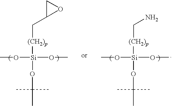
- An example of a reactive organosilane comprises the structure
- the reactive group R may comprise, for example, the structures
- an inert organosilane comprises the structure
- the reactive organosilane comprises the structure
- hydrophobic material comprises the structure
- R is a reactive group
- X is independently at each occurrence a hydrogen or halogen
- n 1-20
- q 1-20.
- the reactive group R may be as described above.
- the distance between the upper surface of the second thin metal film and the reactive group R on the reactive organosilane, and the distance between the upper surface of the second thin metal film and the non-bonded terminus of the hydrophobic material are controlled through the appropriate selection of alkyl (—(CH 2 ) n —), or haloalkyl (—(CX 2 ) q —, where X is a halogen) chain lengths.
- Another embodiment is a process comprising: a) depositing a first metal film on a substrate; b) depositing a second thin metal film on the first metal film; c) converting the upper surface of the second thin metal film to the corresponding metal oxide; and d) reacting a functionalized organosilane with the metal oxide, whereby a reactive organosilane is formed on the upper surface of the second thin metal film.
- the first metal film, the second thin metal film, and the substrate may be as described above.
- converting the upper surface of the second thin metal film to the corresponding metal oxide comprises oxygen plasma treatment.
- the functionalized organosilane is
- the reactive organosilane is N-(2-aminoethyl)-2-aminoethyl
- the process further comprises patterning the reactive organosilane into a plurality of spots. In one embodiment, the process further comprises reacting the reactive organosilane with DNA or RNA.
- Another embodiment is a process comprising: a) depositing a first metal film on a substrate; b) depositing a second thin metal film on the first metal film; c) converting the upper surface of the second thin metal film to the corresponding metal oxide; d) reacting an inert organosilane on the upper surface of the second thin metal film; e) patterning the inert organosilane to give a pattern of a plurality of metal oxide spots surrounded by inert organosilane; and f) reacting a functionalized organosilane with the metal oxide, whereby a reactive organosilane is formed in the metal oxide spots on the second thin metal film.
- Another embodiment is a process comprising: a) depositing a first metal film on a substrate; b) depositing a second thin metal film on the first metal film; c) converting the upper surface of the second thin metal film to the corresponding metal oxide; d) patterning a photoresist on the upper surface into a plurality of spots, the upper surface being exposed between spots; e) reacting an inert organosilane on the metal oxide of the upper surface; f) removing the photoresist to form a plurality of metal oxide spots; and g) reacting a functionalized organosilane with the metal oxide, whereby a reactive organosilane is formed in the metal oxide spots.
- a similar embodiment is a process comprising: a) depositing a first metal film on a substrate; b) depositing second thin metal film on the first metal film; c) patterning a photoresist on the upper surface into a plurality of spots, the surface of the second thin metal film being exposed between spots; d) converting the surface of the second thin metal film between spots to a metal oxide; e) reacting an inert organosilane with the metal oxide of the second thin metal film; f) removing the photoresist to form a plurality of spots comprising the surface of the second thin metal film; g) converting the surface of the second thin metal film in the spots into a metal oxide, whereby a plurality of metal oxide spots is formed; and h) reacting a functionalized organosilane with the metal oxide spots, whereby a reactive organosilane is formed in the metal oxide spots on the second thin metal film.
- the substrate, the first metal film, and the second thin metal film may be as described above.
- the functionalized organosilane and the reactive organosilane may be as described above.
- the reactive organosilane is
- each spot is typically 10-1000 ⁇ m in diameter, and the number the density of spots is typically 100 to 1 million spots per square centimeter.
- the distance between the upper surface of the second thin metal film and the reactive group R on the reactive organosilane, and the distance between the upper surface of the second thin metal film and the non-bonded terminus of the hydrophobic material are controlled through the appropriate selection of alkyl (—(CH 2 ) n —), or haloalkyl (—(CX 2 ) q —, where X is a halogen) chain lengths.
- Another embodiment is a method, comprising a) providing an article including: i) a substrate; ii) a first metal film overlying the substrate; iii) a second thin metal film overlying the first metal film; iv) an organosilane covalently bonded to the upper surface of the second thin metal film through metal-oxygen-silicon bonds; and v) a binding group attached to the organosilane; and b) determining whether or not the biomolecule is bound to the binding group by detecting or measuring a surface plasmon resonance signal generated from the first metal film.
- the binding group comprises DNA or RNA.
- the biomolecule is typically DNA, RNA, or a protein.
- the binding group is an antigen, an antibody, or a hapten.
- the organosilane may have a pattern of a plurality of spots.
- the spots may be arranged in a microarray.
- the size of each spot is typically 10-1000 ⁇ m in diameter, and the number the density of spots is typically 100 to 1 million spots per square centimeter.
- the first metal film, the second thin metal film, and the glass substrate may be as described above.
- a glass substrate was cleaned using Diamaflow 688C.
- the substrate was soaked in a 1% solution of Diamaflow 688C in DI-water (18M ⁇ ) with and sonicated for 5 minutes. After sonication, the samples were brushed in a fresh solution of Diamaflow and DI-water and sonicated again in DI-water at 30° C. in 15 minutes.
- the substrate was rinsed for 5 minutes and dried with filtered N 2 gas. Before the metal deposition the substrate was treated with high pressure O 2 plasma for 5 minutes. The plasma cleaning process should happen right before the metal deposition otherwise the surface conditions cannot be precisely controlled.
- the metal deposition was performed in a Denton Discovery 18 DC magnetron sputtering machine. The base pressure was less than 2 ⁇ 10 ⁇ 7 Torr.
- Argon was used as process gas at a pressure of 7.5 mTorr during deposition.
- the magnetron current was set to 250 mA.
- a 2 nm thick adhesion layer of Cr was deposited followed by deposition of a 47 nm Au layer, followed by deposition of a 10 nm thick layer of Ti.
- Deposition of the inert hydrophobic organosilane and reactive organosilane are shown schematically in cross section in FIGS. 1-2 .
- the substrate was photolithographically patterned with photoresist ( 1 ) squares (100-200 ⁇ m on one side).
- photoresist 1
- O 2 -plasma treatment was used to enhance the bonding of the hydrophobic silane to the Ti.
- a solution of 1H, 1H, 2H, 2H perfluoroundecyl trichlorosilane was spin deposited, rinsed with toluene, and dried with N 2 gas.
- the remaining photoresist was removed using a stripper, washed with an isopropyl alcohol and DI-water rinse, and dried with filtered N 2 gas.
- the Ti surface ( 2 ) was exposed as a series of spots surrounded by the hydrophobic silane ( 3 ).
- the exposed Ti surface was treated with O 2 plasma.
- (Glycidoxypropoxy)trimethoxysilane was spin deposited as described above for the hydrophobic silane to give the reactive organosilane ( 4 ) patterned into series of spots, with each spot surrounded by the hydrophobic organosilane ( 3 ).
- the epoxy-reactive silane was converted to a hydroxy-reactive silane by treatment with H 2 O/HCl ( FIG. 3 ) or ethylene glycol ( FIG. 4 ).
Abstract
Description
- All patents, patent applications, and publications cited within this application are incorporated herein by reference to the same extent as if each individual patent, patent application or publication was specifically and individually incorporated by reference.
- The invention relates generally to surface plasmon resonance substrates and associated methods of analyzing biomolecules. In order to analyze a DNA using surface plasmon resonance (SPR) detection, a metal such as gold having a certain thickness is required on the substrate. For application where DNA is deposited on top of gold there is the problem that gold coated glass slides have not been able to survive DNA printing processes that require corrosive oxidizers, with the gold delaminating from the surface. The gold surface must be modified by using different functionalities, the most popular being thiol chemistry. However, the Au—S bonds are vulnerable to aggressive oxidizers used for some DNA printing process. Thus, there is a need for SPR slides that are able to withstand strong oxidizers used in some DNA printing processes.
- One embodiment is an article comprising: a) a substrate; b) a first metal film overlying the substrate; c) a second thin metal film, the second thin metal film having a first surface facing the first metal film, and a second surface opposed to the first surface; and d) a reactive organosilane covalently bonded to the second surface of the second thin metal film through metal-oxygen-silicon bonds. The second surface opposed to the first surface in the second thin metal film is hereafter referred to as the “upper” surface of the second thin metal film. The first metal film may be gold, silver, or copper and the second thin metal film may be Ti, Zr, Al, Cr, Hf, V, Ta, W, or Pb. Typically, the first metal film can generate surface plasmons and the upper surface of the second thin metal film is used to form chemically stable bonds to the reactive organosilane. As used herein the second thin metal film is sufficiently thin so as to allow extension of an evanescent plasmon wave from said first metal film. The resulting chips can be cleaned with aggressive oxidizers and biomolecules such as DNA, RNA, or proteins can be printed on the reactive organosilane. Chemical interactions with the printed DNA, RNA, or proteins can then be monitored through surface plasmon resonance methods. The second thin metal film may also generate surface plasmons that may interact with the surface plasmons or with surface plasmon effects from the first metal film.
- Another embodiment is a process comprising: a) depositing a first metal film on a substrate; b) depositing a second thin metal film on the first metal film; c) converting the upper surface of the second thin metal film to the corresponding metal oxide; and d) reacting a functionalized organosilane with the metal oxide, whereby a reactive organosilane is formed on the upper surface of the second thin metal film. The organosilanes used typically have a reactive silane moiety and an organic substituent (i.e., trichloro-organosilanes). The terms “functionalized” and “inert” when used in connection with “organosilane” refers to the organic substituent of the silane and not the silane moiety. Another embodiment is a process comprising: a) depositing a first metal film on a substrate; b) depositing second thin metal film on the first metal film; c) converting the upper surface of the second thin metal film to the corresponding metal oxide; d) reacting an inert organosilane with the metal oxide; e) patterning the inert organosilane to give a pattern of a plurality of metal oxide spots surrounded by inert organosilane; and f) reacting a functionalized organosilane with the metal oxide, whereby a reactive organosilane is formed in the metal oxide spots on the second thin metal film. Another embodiment is a process comprising: a) depositing a first metal film on a substrate; b) depositing a second thin metal film on the first metal film; c) converting the upper surface of the second thin metal film to the corresponding metal oxide; d) applying a patterned photoresist on the upper surface defining a plurality of spots, the upper surface being exposed between spots; e) reacting an inert organosilane on the metal oxide of the upper surface; f) removing the photoresist to form a plurality of metal oxide spots; and g) reacting a functionalized organosilane with the metal oxide, whereby a reactive organosilane is formed in the metal oxide spots. A similar embodiment is a process comprising: a) depositing a first metal film on a substrate; b) depositing second thin metal film on the first metal film; c) patterning a photoresist on the upper surface into a plurality of spots, the surface of the second thin metal film being exposed between spots; d) converting the surface of the second thin metal film between spots to a metal oxide; e) reacting an inert organosilane with the metal oxide of the second thin metal film; f) removing the photoresist to form a plurality of spots comprising the surface of the second thin metal film; g) converting the surface of the second thin metal film in the spots into a metal oxide, whereby a plurality of metal oxide spots is formed; and h) reacting a functionalized organosilane with the metal oxide spots, whereby a reactive organosilane is formed in the metal oxide spots on the second thin metal film.
- Another embodiment is a method, comprising a) providing an article including: i) a substrate; ii) a first metal film overlying the substrate; iii) a second thin metal film overlying the first metal film; iv) an organosilane covalently bonded to the exposed upper surface of the second thin metal film through metal-oxygen-silicon bonds; v) a binding group attached to the organosilane; b) contacting the article with a biomolecule; and c) determining whether or not the biomolecule is bound to the binding group by detecting or measuring a surface plasmon resonance signal generated from the first metal film.
-
FIG. 1 is a cross-sectional view of a process scheme. -
FIG. 2 is a cross-sectional view of a process scheme. -
FIG. 3 is a cross sectional view of a process scheme. -
FIG. 4 is a cross-sectional view of a process scheme. - One embodiment is an article comprising: a) a substrate; b) a first metal film overlying the substrate; c) a second thin metal film overlying the first metal film; and d) a reactive organosilane covalently bonded to the upper surface of the second thin metal film through metal-oxygen-silicon bonds. The first metal film may be gold, silver, or copper and the second thin metal film may be Ti, Zr, Al, Cr, Hf, V, Ta, W, or Pb. Typically, the first metal film can generate surface plasmons and the upper surface of the second metal film is used to form chemically stable bonds to the reactive organosilane. When the second thin metal film is sufficiently thin, the evanescent wave of the surface plasmons generated by the first metal film extend through the second thin metal film and can be used to detect chemical changes near the upper surface of the second thin metal film. Detecting these chemical changes can be used, for example, to monitor biological molecule binding and image dielectric thin films. Typically, the substrate is glass or quartz. In other embodiments, the substrate comprises one face of a prism. The article may further comprise an adhesion metal layer between the substrate and the first metal film. The adhesion metal layer typically is Cr, Ti, W, or any combination thereof.
- In many embodiments, the reactive organosilane has a pattern on the surface that is a plurality of spots. In most embodiments, the spots are arranged in a microarray. Hydrophobic material may surround one or more of the reactive organosilane spots. The hydrophobic material may cause a polar liquid (e.g., water) to bead on the reactive organosilane spot, which allows the spot to be used as a microwell. The size of each spot is typically 10-1000 μm in diameter, and the density of spots is typically 100 to 1 million spots per square centimeter. The hydrophobic material typically comprises an inert organosilane covalently bonded to the upper surface of the second thin metal film through metal-oxygen-silicon bonds. The inert organosilane may include, for example, a fluorinated alkyl group. In many embodiments, the reactive organosilane comprises hydroxy groups. The hydroxy groups may be capped with DNA or RNA (e.g., DNA or RNA have been reacted with the hydroxyl groups to form covalent bonds). An example of a reactive organosilane comprises the structure
-

- wherein: R is a reactive group and n=1-20. The reactive group R may comprise, for example, the structures
-

- wherein m=1-10. One example of an inert organosilane comprises the structure
-

- wherein: q=1-4; and p=1-20. In some embodiments, the reactive organosilane comprises the structure
-

- and the hydrophobic material comprises the structure
-

- wherein: R is a reactive group; X is independently at each occurrence a hydrogen or halogen; n=1-20; and q=1-20. The reactive group R may be as described above. The distance between the upper surface of the second thin metal film and the reactive group R on the reactive organosilane, and the distance between the upper surface of the second thin metal film and the non-bonded terminus of the hydrophobic material are controlled through the appropriate selection of alkyl (—(CH2)n—), or haloalkyl (—(CX2)q—, where X is a halogen) chain lengths.
- Another embodiment is a process comprising: a) depositing a first metal film on a substrate; b) depositing a second thin metal film on the first metal film; c) converting the upper surface of the second thin metal film to the corresponding metal oxide; and d) reacting a functionalized organosilane with the metal oxide, whereby a reactive organosilane is formed on the upper surface of the second thin metal film. The first metal film, the second thin metal film, and the substrate may be as described above. In many embodiments, converting the upper surface of the second thin metal film to the corresponding metal oxide comprises oxygen plasma treatment. In one embodiment, the functionalized organosilane is
-

- wherein: R3 is chlorine or alkoxy; p=1-20; and the reactive organosilane comprises
-

- In other embodiments, the reactive organosilane is
-

- and the process further comprises converting the reactive organosilane to
-

- In some embodiments, the process further comprises patterning the reactive organosilane into a plurality of spots. In one embodiment, the process further comprises reacting the reactive organosilane with DNA or RNA.
- Another embodiment is a process comprising: a) depositing a first metal film on a substrate; b) depositing a second thin metal film on the first metal film; c) converting the upper surface of the second thin metal film to the corresponding metal oxide; d) reacting an inert organosilane on the upper surface of the second thin metal film; e) patterning the inert organosilane to give a pattern of a plurality of metal oxide spots surrounded by inert organosilane; and f) reacting a functionalized organosilane with the metal oxide, whereby a reactive organosilane is formed in the metal oxide spots on the second thin metal film. Another embodiment is a process comprising: a) depositing a first metal film on a substrate; b) depositing a second thin metal film on the first metal film; c) converting the upper surface of the second thin metal film to the corresponding metal oxide; d) patterning a photoresist on the upper surface into a plurality of spots, the upper surface being exposed between spots; e) reacting an inert organosilane on the metal oxide of the upper surface; f) removing the photoresist to form a plurality of metal oxide spots; and g) reacting a functionalized organosilane with the metal oxide, whereby a reactive organosilane is formed in the metal oxide spots. A similar embodiment is a process comprising: a) depositing a first metal film on a substrate; b) depositing second thin metal film on the first metal film; c) patterning a photoresist on the upper surface into a plurality of spots, the surface of the second thin metal film being exposed between spots; d) converting the surface of the second thin metal film between spots to a metal oxide; e) reacting an inert organosilane with the metal oxide of the second thin metal film; f) removing the photoresist to form a plurality of spots comprising the surface of the second thin metal film; g) converting the surface of the second thin metal film in the spots into a metal oxide, whereby a plurality of metal oxide spots is formed; and h) reacting a functionalized organosilane with the metal oxide spots, whereby a reactive organosilane is formed in the metal oxide spots on the second thin metal film. The substrate, the first metal film, and the second thin metal film may be as described above. The inert organosilane typically includes a fluorinated alkyl group, for example the structure
-

- wherein: q=1-4; and p=1-20. The functionalized organosilane and the reactive organosilane may be as described above. In one embodiment, the reactive organosilane is
-

- and the process further comprises converting the reactive organosilane to
-

- The size of each spot is typically 10-1000 μm in diameter, and the number the density of spots is typically 100 to 1 million spots per square centimeter. The distance between the upper surface of the second thin metal film and the reactive group R on the reactive organosilane, and the distance between the upper surface of the second thin metal film and the non-bonded terminus of the hydrophobic material are controlled through the appropriate selection of alkyl (—(CH2)n—), or haloalkyl (—(CX2)q—, where X is a halogen) chain lengths.
- Another embodiment is a method, comprising a) providing an article including: i) a substrate; ii) a first metal film overlying the substrate; iii) a second thin metal film overlying the first metal film; iv) an organosilane covalently bonded to the upper surface of the second thin metal film through metal-oxygen-silicon bonds; and v) a binding group attached to the organosilane; and b) determining whether or not the biomolecule is bound to the binding group by detecting or measuring a surface plasmon resonance signal generated from the first metal film. In some embodiments, the binding group comprises DNA or RNA. The biomolecule is typically DNA, RNA, or a protein. In other embodiments, the binding group is an antigen, an antibody, or a hapten. The organosilane may have a pattern of a plurality of spots. The spots may be arranged in a microarray. The size of each spot is typically 10-1000 μm in diameter, and the number the density of spots is typically 100 to 1 million spots per square centimeter. The first metal film, the second thin metal film, and the glass substrate may be as described above.
- The following example(s) is illustrative and does not limit the Claims.
- A glass substrate was cleaned using Diamaflow 688C. The substrate was soaked in a 1% solution of Diamaflow 688C in DI-water (18MΩ) with and sonicated for 5 minutes. After sonication, the samples were brushed in a fresh solution of Diamaflow and DI-water and sonicated again in DI-water at 30° C. in 15 minutes. The substrate was rinsed for 5 minutes and dried with filtered N2 gas. Before the metal deposition the substrate was treated with high pressure O2 plasma for 5 minutes. The plasma cleaning process should happen right before the metal deposition otherwise the surface conditions cannot be precisely controlled. The metal deposition was performed in a Denton Discovery 18 DC magnetron sputtering machine. The base pressure was less than 2×10⁻⁷ Torr. Argon was used as process gas at a pressure of 7.5 mTorr during deposition. The magnetron current was set to 250 mA. First, a 2 nm thick adhesion layer of Cr was deposited followed by deposition of a 47 nm Au layer, followed by deposition of a 10 nm thick layer of Ti.
- Deposition of the inert hydrophobic organosilane and reactive organosilane are shown schematically in cross section in
FIGS. 1-2 . After metal deposition the substrate was photolithographically patterned with photoresist (1) squares (100-200 μm on one side). Following development, an O2-plasma treatment was used to enhance the bonding of the hydrophobic silane to the Ti. A solution of 1H, 1H, 2H, 2H perfluoroundecyl trichlorosilane was spin deposited, rinsed with toluene, and dried with N2 gas. The remaining photoresist was removed using a stripper, washed with an isopropyl alcohol and DI-water rinse, and dried with filtered N2 gas. At this point the Ti surface (2) was exposed as a series of spots surrounded by the hydrophobic silane (3). The exposed Ti surface was treated with O2 plasma. (Glycidoxypropoxy)trimethoxysilane was spin deposited as described above for the hydrophobic silane to give the reactive organosilane (4) patterned into series of spots, with each spot surrounded by the hydrophobic organosilane (3). The epoxy-reactive silane was converted to a hydroxy-reactive silane by treatment with H2O/HCl (FIG. 3 ) or ethylene glycol (FIG. 4 ).
Claims (26)


Priority Applications (2)
| Application Number | Priority Date | Filing Date | Title |
|---|---|---|---|
| US12/330,384 US8094315B2 (en) | 2005-12-06 | 2008-12-08 | Methods for making and using SPR microarrays |
| US13/337,506 US20120115748A1 (en) | 2005-12-06 | 2011-12-27 | Methods for making and using spr microarrays |
Applications Claiming Priority (2)
| Application Number | Priority Date | Filing Date | Title |
|---|---|---|---|
| US11/296,659 US7463358B2 (en) | 2005-12-06 | 2005-12-06 | Highly stable surface plasmon resonance plates, microarrays, and methods |
| US12/330,384 US8094315B2 (en) | 2005-12-06 | 2008-12-08 | Methods for making and using SPR microarrays |
Related Parent Applications (1)
| Application Number | Title | Priority Date | Filing Date |
|---|---|---|---|
| US11/296,659 Division US7463358B2 (en) | 2005-12-06 | 2005-12-06 | Highly stable surface plasmon resonance plates, microarrays, and methods |
Related Child Applications (1)
| Application Number | Title | Priority Date | Filing Date |
|---|---|---|---|
| US13/337,506 Continuation US20120115748A1 (en) | 2005-12-06 | 2011-12-27 | Methods for making and using spr microarrays |
Publications (2)
| Publication Number | Publication Date |
|---|---|
| US20090093067A1 true US20090093067A1 (en) | 2009-04-09 |
| US8094315B2 US8094315B2 (en) | 2012-01-10 |
Family
ID=38119131
Family Applications (3)
| Application Number | Title | Priority Date | Filing Date |
|---|---|---|---|
| US11/296,659 Active 2026-05-28 US7463358B2 (en) | 2005-12-06 | 2005-12-06 | Highly stable surface plasmon resonance plates, microarrays, and methods |
| US12/330,384 Active 2026-10-20 US8094315B2 (en) | 2005-12-06 | 2008-12-08 | Methods for making and using SPR microarrays |
| US13/337,506 Abandoned US20120115748A1 (en) | 2005-12-06 | 2011-12-27 | Methods for making and using spr microarrays |
Family Applications Before (1)
| Application Number | Title | Priority Date | Filing Date |
|---|---|---|---|
| US11/296,659 Active 2026-05-28 US7463358B2 (en) | 2005-12-06 | 2005-12-06 | Highly stable surface plasmon resonance plates, microarrays, and methods |
Family Applications After (1)
| Application Number | Title | Priority Date | Filing Date |
|---|---|---|---|
| US13/337,506 Abandoned US20120115748A1 (en) | 2005-12-06 | 2011-12-27 | Methods for making and using spr microarrays |
Country Status (1)
| Country | Link |
|---|---|
| US (3) | US7463358B2 (en) |
Cited By (1)
| Publication number | Priority date | Publication date | Assignee | Title |
|---|---|---|---|---|
| US20090060786A1 (en) * | 2007-08-29 | 2009-03-05 | Gibum Kim | Microfluidic apparatus for wide area microarrays |
Families Citing this family (11)
| Publication number | Priority date | Publication date | Assignee | Title |
|---|---|---|---|---|
| US20040258832A1 (en) * | 2003-06-17 | 2004-12-23 | Barklund Anna M. | Method of chemical analysis using microwells patterned from self-assembled monolayers and substrates |
| US7745143B2 (en) * | 2004-11-19 | 2010-06-29 | Plexera, Llc | Plasmon resonance biosensor and method |
| US20090262356A1 (en) * | 2008-03-27 | 2009-10-22 | Plexera, Llc | User interface and method for using an spr system |
| US7889347B2 (en) | 2005-11-21 | 2011-02-15 | Plexera Llc | Surface plasmon resonance spectrometer with an actuator driven angle scanning mechanism |
| US7463358B2 (en) | 2005-12-06 | 2008-12-09 | Lumera Corporation | Highly stable surface plasmon resonance plates, microarrays, and methods |
| US8263377B2 (en) | 2007-04-03 | 2012-09-11 | Plexera, Llc | Label free kinase assays and reagents |
| US7695976B2 (en) * | 2007-08-29 | 2010-04-13 | Plexera Bioscience, Llc | Method for uniform analyte fluid delivery to microarrays |
| US8004669B1 (en) | 2007-12-18 | 2011-08-23 | Plexera Llc | SPR apparatus with a high performance fluid delivery system |
| JP4572244B2 (en) * | 2008-04-09 | 2010-11-04 | シャープ株式会社 | Surface plasmon sensor |
| CN104374746A (en) * | 2014-10-27 | 2015-02-25 | 李博 | Method for preparing surface plasma resonance chip by taking silver as target |
| WO2023049192A1 (en) * | 2021-09-22 | 2023-03-30 | Ultima Genomics, Inc. | Methods and systems for substrate functionalization |
Citations (93)
| Publication number | Priority date | Publication date | Assignee | Title |
|---|---|---|---|---|
| US3751587A (en) * | 1972-01-20 | 1973-08-07 | Saxon Ind Inc | Laser printing system |
| US3891507A (en) * | 1974-05-30 | 1975-06-24 | American Cyanamid Co | Organ function test cards |
| US4038030A (en) * | 1975-04-10 | 1977-07-26 | American Hospital Supply Corporation | Profile analysis pack and method |
| US4148057A (en) * | 1977-10-25 | 1979-04-03 | Solution Sciences, Inc. | Direct laser printing and forming apparatus |
| US4375025A (en) * | 1980-06-19 | 1983-02-22 | Automated Industrial Systems, Inc. | Laser strip marker |
| US4585931A (en) * | 1983-11-21 | 1986-04-29 | At&T Technologies, Inc. | Method for automatically identifying semiconductor wafers |
| US4638144A (en) * | 1985-04-24 | 1987-01-20 | Automated Industrial Systems | Indexing laser marker |
| US4719502A (en) * | 1985-08-07 | 1988-01-12 | Kabushiki Kaisha Toshiba | Epoxy resin composition, and resin-sealed semiconductor device in which this composition is used |
| US4753863A (en) * | 1985-02-01 | 1988-06-28 | Motorola Inc. | Laser markable molding compound |
| US4945045A (en) * | 1984-07-06 | 1990-07-31 | Serono Diagnostics Ltd. | Electrochemical methods of assay |
| US4945204A (en) * | 1988-11-10 | 1990-07-31 | Mitsubishi Denki Kabushiki Kaisha | Method of laser-marking semiconductor devices |
| US4997278A (en) * | 1987-08-22 | 1991-03-05 | Amersham International Plc | Biological sensors |
| US5030551A (en) * | 1989-04-06 | 1991-07-09 | Ciba-Geigy Corporation | Laser marking of ceramic materials, glazes, glass ceramics and glasses |
| US5078855A (en) * | 1987-10-13 | 1992-01-07 | Taiyo Yuden Co., Ltd. | Chemical sensors and their divided parts |
| US5089112A (en) * | 1989-03-20 | 1992-02-18 | Associated Universities, Inc. | Electrochemical biosensor based on immobilized enzymes and redox polymers |
| US5104619A (en) * | 1990-01-24 | 1992-04-14 | Gds Technology, Inc. | Disposable diagnostic system |
| US5116481A (en) * | 1989-04-07 | 1992-05-26 | Hitachi, Ltd. | Anion-selective, sensitive film, electrode containing the same and the use thereof |
| US5192507A (en) * | 1987-06-05 | 1993-03-09 | Arthur D. Little, Inc. | Receptor-based biosensors |
| US5197599A (en) * | 1990-04-05 | 1993-03-30 | Chicago Tribune Company | Sample packet adapted for insertion into a newspaper |
| US5200051A (en) * | 1988-11-14 | 1993-04-06 | I-Stat Corporation | Wholly microfabricated biosensors and process for the manufacture and use thereof |
| US5206280A (en) * | 1990-03-15 | 1993-04-27 | British Aerospace Public Limited Company | Laser markable white pigment composition |
| US5225047A (en) * | 1987-01-20 | 1993-07-06 | Weyerhaeuser Company | Crosslinked cellulose products and method for their preparation |
| US5313264A (en) * | 1988-11-10 | 1994-05-17 | Pharmacia Biosensor Ab | Optical biosensor system |
| US5329090A (en) * | 1993-04-09 | 1994-07-12 | A B Lasers, Inc. | Writing on silicon wafers |
| US5401378A (en) * | 1991-03-27 | 1995-03-28 | Australian Membrane & Biotechnology Research Institute | Ionic reservoir at electrode surface |
| US5405783A (en) * | 1989-06-07 | 1995-04-11 | Affymax Technologies N.V. | Large scale photolithographic solid phase synthesis of an array of polymers |
| US5413629A (en) * | 1992-11-30 | 1995-05-09 | Dainippon Ink And Chemicals, Inc. | Laser marking and printing ink therefor |
| US5415838A (en) * | 1993-02-10 | 1995-05-16 | Dragerwerk Aktiengesellschaft | Carrier for colorimetrically detecting a gas |
| US5436170A (en) * | 1987-07-27 | 1995-07-25 | Commonwealth Scientific And Industrial Research Organization | Receptor membranes |
| US5436161A (en) * | 1988-11-10 | 1995-07-25 | Pharmacia Biosensor Ab | Matrix coating for sensing surfaces capable of selective biomolecular interactions, to be used in biosensor systems |
| US5485277A (en) * | 1994-07-26 | 1996-01-16 | Physical Optics Corporation | Surface plasmon resonance sensor and methods for the utilization thereof |
| US5491097A (en) * | 1989-06-15 | 1996-02-13 | Biocircuits Corporation | Analyte detection with multilayered bioelectronic conductivity sensors |
| US5492840A (en) * | 1988-11-10 | 1996-02-20 | Pharmacia Biosensor Ab | Surface plasmon resonance sensor unit and its use in biosensor systems |
| US5512131A (en) * | 1993-10-04 | 1996-04-30 | President And Fellows Of Harvard College | Formation of microstamped patterns on surfaces and derivative articles |
| US5514501A (en) * | 1994-06-07 | 1996-05-07 | The United States Of America As Represented By The Secretary Of Commerce | Process for UV-photopatterning of thiolate monolayers self-assembled on gold, silver and other substrates |
| US5527711A (en) * | 1993-12-13 | 1996-06-18 | Hewlett Packard Company | Method and reagents for binding chemical analytes to a substrate surface, and related analytical devices and diagnostic techniques |
| US5536822A (en) * | 1994-03-09 | 1996-07-16 | University Of Virginia Alumni Patents Foundation | γ-phosphate linked adenosine 5' triphosphate sepharose |
| US5624537A (en) * | 1994-09-20 | 1997-04-29 | The University Of British Columbia - University-Industry Liaison Office | Biosensor and interface membrane |
| US5629790A (en) * | 1993-10-18 | 1997-05-13 | Neukermans; Armand P. | Micromachined torsional scanner |
| US5637201A (en) * | 1992-10-01 | 1997-06-10 | Australian Membrane And Biotechnology Research Ins. | Sensor membranes |
| US5707502A (en) * | 1996-07-12 | 1998-01-13 | Chiron Diagnostics Corporation | Sensors for measuring analyte concentrations and methods of making same |
| US5716778A (en) * | 1985-02-14 | 1998-02-10 | Abbott Laboratories | Concentrating immunochemical test device and method |
| US5719060A (en) * | 1993-05-28 | 1998-02-17 | Baylor College Of Medicine | Method and apparatus for desorption and ionization of analytes |
| US5723345A (en) * | 1994-06-28 | 1998-03-03 | Mochida Pharmaceutical Co., Ltd. | Method and device for specific binding assay |
| US5736410A (en) * | 1992-09-14 | 1998-04-07 | Sri International | Up-converting reporters for biological and other assays using laser excitation techniques |
| US5756355A (en) * | 1992-04-22 | 1998-05-26 | Ecole Polytechnique Federale De Lausanne | Lipid membrane sensors |
| US5922594A (en) * | 1994-09-26 | 1999-07-13 | Biacore Ab | Method of producing bilayer lipid membranes |
| US5922617A (en) * | 1997-11-12 | 1999-07-13 | Functional Genetics, Inc. | Rapid screening assay methods and devices |
| US6020208A (en) * | 1994-05-27 | 2000-02-01 | Baylor College Of Medicine | Systems for surface-enhanced affinity capture for desorption and detection of analytes |
| US6074616A (en) * | 1998-01-05 | 2000-06-13 | Biosite Diagnostics, Inc. | Media carrier for an assay device |
| US6218194B1 (en) * | 1996-02-08 | 2001-04-17 | Thermo Fast Uk Limited | Analytical methods and apparatus employing an optical sensor device with refractive index modulation |
| US6219138B1 (en) * | 2000-01-10 | 2001-04-17 | The United States Of America As Represented By The Secretary Of The Navy | Particle sizing technique |
| US6217949B1 (en) * | 1996-01-11 | 2001-04-17 | Micron Technology, Inc. | Laser marking techniques |
| US6232066B1 (en) * | 1997-12-19 | 2001-05-15 | Neogen, Inc. | High throughput assay system |
| US6245590B1 (en) * | 1999-08-05 | 2001-06-12 | Microvision Inc. | Frequency tunable resonant scanner and method of making |
| US6340597B1 (en) * | 1995-07-05 | 2002-01-22 | Saicom S.R.L. | Electrochemical biosensors and process for their preparation |
| US20020024495A1 (en) * | 1998-08-05 | 2002-02-28 | Microvision, Inc. | Scanned beam display |
| US6362912B1 (en) * | 1999-08-05 | 2002-03-26 | Microvision, Inc. | Scanned imaging apparatus with switched feeds |
| US20020044893A1 (en) * | 1999-08-05 | 2002-04-18 | Robert M. Corn | Biomolecule and/or cellular arrays on metal surfaces |
| US6380365B1 (en) * | 1998-09-04 | 2002-04-30 | Affitech As | Temperature dependent ligand facilitated purification of proteins |
| US6379929B1 (en) * | 1996-11-20 | 2002-04-30 | The Regents Of The University Of Michigan | Chip-based isothermal amplification devices and methods |
| US20020068813A1 (en) * | 2000-02-29 | 2002-06-06 | Tatjana Dragic | Sulfated CCR5 peptides for HIV-1 infection |
| US6406921B1 (en) * | 1998-07-14 | 2002-06-18 | Zyomyx, Incorporated | Protein arrays for high-throughput screening |
| US6421164B2 (en) * | 1991-04-29 | 2002-07-16 | Massachusetts Institute Of Technology | Interferometeric imaging with a grating based phase control optical delay line |
| US6545758B1 (en) * | 2000-08-17 | 2003-04-08 | Perry Sandstrom | Microarray detector and synthesizer |
| US6548171B1 (en) * | 1998-11-10 | 2003-04-15 | Emilio Barbera-Guillem | Fluorescent nanocrystal-embedded microspheres for fluorescence analyses |
| US20030082820A1 (en) * | 2001-10-18 | 2003-05-01 | Perbost Michel G.M. | Chemical arrays |
| US6558623B1 (en) * | 2000-07-06 | 2003-05-06 | Robodesign International, Inc. | Microarray dispensing with real-time verification and inspection |
| US6565813B1 (en) * | 1998-02-04 | 2003-05-20 | Merck & Co., Inc. | Virtual wells for use in high throughput screening assays |
| US6569385B1 (en) * | 1997-01-23 | 2003-05-27 | Sequenom, Inc. | Systems and methods for preparing and analyzing low volume analyte array elements |
| US20030107741A1 (en) * | 2001-12-11 | 2003-06-12 | Pyo Hyeon Bong | Surface plasmon resonance sensor system |
| US6583193B2 (en) * | 2000-03-17 | 2003-06-24 | Dow Global Technologies Inc. | Polyolefin foam useful for sound and thermal insulation |
| US20040008345A1 (en) * | 2002-05-20 | 2004-01-15 | Nurmikko Arto V. | Optical tracking and detection of particles by solid state energy sources |
| US20040014946A1 (en) * | 2002-04-25 | 2004-01-22 | Heman Chao | Protein interaction method and composition |
| US20040048311A1 (en) * | 2002-01-24 | 2004-03-11 | Dana Ault-Riche | Use of collections of binding sites for sample profiling and other applications |
| US20040067597A1 (en) * | 2002-07-31 | 2004-04-08 | Caliper Technologies Corp. | High density reagent array preparation methods |
| US20050002085A1 (en) * | 2003-05-07 | 2005-01-06 | Funai Electric Co., Ltd. | MEMS mirror device and optical disk apparatus |
| US20050046848A1 (en) * | 2003-08-26 | 2005-03-03 | Blueshift Biotechnologies, Inc. | Time dependent fluorescence measurements |
| US6870627B2 (en) * | 2001-03-30 | 2005-03-22 | Texas Instruments Incorporated | System for directed molecular interaction in surface plasmon resonance analysis |
| US20050095577A1 (en) * | 2003-10-31 | 2005-05-05 | Yang Dan-Hui D. | Protein bioarray on silane-modified substrate surface |
| US6902705B1 (en) * | 1998-09-16 | 2005-06-07 | Commissariat A L'energie Atomique | Device comprising a plurality of analysis sites on a support |
| US6911344B1 (en) * | 1996-08-28 | 2005-06-28 | Biocentrex, Llc | Composite waveguide for solid phase binding assays |
| US20060091051A1 (en) * | 2003-03-11 | 2006-05-04 | Tetsuo Takada | Micro fluid device and process for producing the same |
| US7041208B2 (en) * | 2001-12-11 | 2006-05-09 | Sau Lan Tang Staats | Microfluidic devices and methods for two-dimensional separations |
| US20060154320A1 (en) * | 2005-01-07 | 2006-07-13 | Fortebio, Inc. | Enzyme activity measurement using bio-layer interferometry |
| US20070009198A1 (en) * | 2004-07-02 | 2007-01-11 | Robert Petcavich | Fiber optic bio-sensor |
| US20070059817A1 (en) * | 2005-09-13 | 2007-03-15 | Canon Kabushiki Kaisha | Biochemical reaction cassette with improved liquid filling performance |
| US20070081163A1 (en) * | 2005-06-03 | 2007-04-12 | Minhua Liang | Method and apparatus for scanned beam microarray assay |
| US20070099180A1 (en) * | 2005-10-31 | 2007-05-03 | Robotti Karla M | Evanescent wave sensor with attached ligand |
| US20070122314A1 (en) * | 2000-10-06 | 2007-05-31 | Protasis Corporation | Microfluidic substrate assembly and method for making same |
| US20070128455A1 (en) * | 2005-12-06 | 2007-06-07 | Nick Wolf | Highly stable surface plasmon resonance plates, microarrays, and methods |
| US20070140918A1 (en) * | 2005-12-19 | 2007-06-21 | Hongfeng Yin | Fluidic separation devices and methods with reduced sample broadening |
| US7319046B2 (en) * | 2001-11-29 | 2008-01-15 | Konstantinos Misiakos | Integrated optoelectronic silicon biosensor for the detection of biomolecules labeled with chromophore groups or nanoparticles |
Family Cites Families (93)
| Publication number | Priority date | Publication date | Assignee | Title |
|---|---|---|---|---|
| US3105902A (en) | 1960-09-19 | 1963-10-01 | Standard Oil Co | Controlled atmosphere X-ray diffraction spectrometer |
| US3990850A (en) | 1976-01-06 | 1976-11-09 | Akzona Incorporated | Diagnostic test card |
| US4707722A (en) | 1984-12-17 | 1987-11-17 | Motorola, Inc. | Laser marking method and ablative coating for use therein |
| EP0215669A3 (en) | 1985-09-17 | 1989-08-30 | Seiko Instruments Inc. | Analytical device and method for analysis of biochemicals, microbes and cells |
| KR910000826B1 (en) | 1986-11-14 | 1991-02-09 | 미쓰비시덴기 가부시기가이샤 | Method of laser marking |
| DE3731835A1 (en) | 1987-09-22 | 1989-03-30 | Siemens Ag | LASER BEAM INDUCED COLOR PRINTING |
| US6054270A (en) | 1988-05-03 | 2000-04-25 | Oxford Gene Technology Limited | Analying polynucleotide sequences |
| WO1990012092A1 (en) | 1989-04-04 | 1990-10-18 | Fritz Pittner | Process for immobilizing proteins, peptides, coenzymes, etc. on a substrate |
| US5744101A (en) | 1989-06-07 | 1998-04-28 | Affymax Technologies N.V. | Photolabile nucleoside protecting groups |
| US6346413B1 (en) | 1989-06-07 | 2002-02-12 | Affymetrix, Inc. | Polymer arrays |
| US5800992A (en) | 1989-06-07 | 1998-09-01 | Fodor; Stephen P.A. | Method of detecting nucleic acids |
| US6379895B1 (en) | 1989-06-07 | 2002-04-30 | Affymetrix, Inc. | Photolithographic and other means for manufacturing arrays |
| US5268305A (en) | 1989-06-15 | 1993-12-07 | Biocircuits Corporation | Multi-optical detection system |
| US5368712A (en) | 1989-11-02 | 1994-11-29 | Synporin Technologies, Inc. | Biologically mimetic synthetic ion channel transducers |
| US5068124A (en) | 1989-11-17 | 1991-11-26 | International Business Machines Corporation | Method for depositing high quality silicon dioxide by pecvd |
| US5478756A (en) | 1990-07-24 | 1995-12-26 | Fisons Plc | Chemical sensor for detecting binding reactions |
| EP0739933B1 (en) | 1990-11-07 | 1999-03-03 | Teijin Limited | Polyester resin composition |
| DE69132843T2 (en) | 1990-12-06 | 2002-09-12 | Affymetrix Inc N D Ges D Staat | Identification of nucleic acids in samples |
| US5474796A (en) | 1991-09-04 | 1995-12-12 | Protogene Laboratories, Inc. | Method and apparatus for conducting an array of chemical reactions on a support surface |
| JP2862413B2 (en) | 1991-10-02 | 1999-03-03 | ポリプラスチックス株式会社 | Laser marking method |
| US5677195A (en) | 1991-11-22 | 1997-10-14 | Affymax Technologies N.V. | Combinatorial strategies for polymer synthesis |
| JP3102822B2 (en) | 1992-05-29 | 2000-10-23 | 日本ジーイープラスチックス株式会社 | Resin composition for laser marking |
| US5445923A (en) | 1992-09-30 | 1995-08-29 | Somar Corporation | Laser beam absorbing resin composition and laser beam marking method |
| JPH0810729B2 (en) | 1993-01-20 | 1996-01-31 | 日本電気株式会社 | Stamping machine |
| US5512492A (en) | 1993-05-18 | 1996-04-30 | University Of Utah Research Foundation | Waveguide immunosensor with coating chemistry providing enhanced sensitivity |
| GB9315847D0 (en) | 1993-07-30 | 1993-09-15 | Isis Innovation | Tag reagent and assay method |
| EP0722563A4 (en) | 1993-08-24 | 1998-03-04 | Metrika Lab Inc | Novel disposable electronic assay device |
| US5470952A (en) | 1993-10-20 | 1995-11-28 | Regeneron Pharmaceuticals, Inc. | CNTF and IL-6 antagonists |
| IL108726A (en) | 1994-02-22 | 1999-12-31 | Yissum Res Dev Co | Electrobiochemical method and system for the determination of an analyte which is a member of a recognition pair in a liquid medium and electrodes therefor |
| FR2720832A1 (en) | 1994-04-22 | 1995-12-08 | Francis Garnier | Electroactive electrodes and membranes based on bioactive peptides, for the recognition, extraction or release of biologically active species. |
| US5824483A (en) | 1994-05-18 | 1998-10-20 | Pence Inc. | Conformationally-restricted combinatiorial library composition and method |
| US6287850B1 (en) | 1995-06-07 | 2001-09-11 | Affymetrix, Inc. | Bioarray chip reaction apparatus and its manufacture |
| DE4430023A1 (en) | 1994-08-24 | 1996-02-29 | Boehringer Mannheim Gmbh | Electrochemical sensor |
| US5688642A (en) | 1994-12-01 | 1997-11-18 | The United States Of America As Represented By The Secretary Of The Navy | Selective attachment of nucleic acid molecules to patterned self-assembled surfaces |
| US5567301A (en) | 1995-03-01 | 1996-10-22 | Illinois Institute Of Technology | Antibody covalently bound film immunobiosensor |
| US5798030A (en) | 1995-05-17 | 1998-08-25 | Australian Membrane And Biotechnology Research Institute | Biosensor membranes |
| US5690894A (en) | 1995-05-23 | 1997-11-25 | The Regents Of The University Of California | High density array fabrication and readout method for a fiber optic biosensor |
| AUPN366995A0 (en) | 1995-06-20 | 1995-07-13 | Australian Membrane And Biotechnology Research Institute | Self-assembly of bilayer membrane sensors |
| US6586193B2 (en) | 1996-04-25 | 2003-07-01 | Genicon Sciences Corporation | Analyte assay using particulate labels |
| US6165335A (en) | 1996-04-25 | 2000-12-26 | Pence And Mcgill University | Biosensor device and method |
| US5955379A (en) | 1996-04-25 | 1999-09-21 | Mcgill University | Biosensor device and method |
| US5938595A (en) | 1996-05-24 | 1999-08-17 | The Regents Of The University Of California | Fiber optic D dimer biosensor |
| SE9700384D0 (en) | 1997-02-04 | 1997-02-04 | Biacore Ab | Analytical method and apparatus |
| US6406845B1 (en) | 1997-05-05 | 2002-06-18 | Trustees Of Tuft College | Fiber optic biosensor for selectively detecting oligonucleotide species in a mixed fluid sample |
| NZ516848A (en) | 1997-06-20 | 2004-03-26 | Ciphergen Biosystems Inc | Retentate chromatography apparatus with applications in biology and medicine |
| US6245506B1 (en) | 1997-07-30 | 2001-06-12 | Bbi Bioseq, Inc. | Integrated sequencing device |
| US6207370B1 (en) | 1997-09-02 | 2001-03-27 | Sequenom, Inc. | Diagnostics based on mass spectrometric detection of translated target polypeptides |
| US6101946A (en) | 1997-11-21 | 2000-08-15 | Telechem International Inc. | Microarray printing device including printing pins with flat tips and exterior channel and method of manufacture |
| EP1038167A4 (en) | 1997-12-12 | 2001-08-22 | Perkin Elmer Corp | Optical resonance analysis system |
| JP2002502588A (en) | 1998-02-06 | 2002-01-29 | アフィメトリックス インコーポレイテッド | Quality control methods in the manufacturing process |
| US6150147A (en) | 1998-02-06 | 2000-11-21 | Affymetrix, Inc. | Biological array fabrication methods with reduction of static charge |
| US6197599B1 (en) | 1998-07-30 | 2001-03-06 | Guorong Chin | Method to detect proteins |
| US6472179B2 (en) | 1998-09-25 | 2002-10-29 | Regeneron Pharmaceuticals, Inc. | Receptor based antagonists and methods of making and using |
| WO2000052456A1 (en) | 1999-03-02 | 2000-09-08 | Helix Biopharma Corporation | Biosensor device and method |
| US6433907B1 (en) | 1999-08-05 | 2002-08-13 | Microvision, Inc. | Scanned display with plurality of scanning assemblies |
| US6448089B1 (en) | 1999-10-12 | 2002-09-10 | Aurora Biosciences Corporation | Multiwell scanner and scanning method |
| US6489106B1 (en) | 2000-03-10 | 2002-12-03 | Nec Research Institute, Inc. | Control of the expression of anchored genes using micron scale heaters |
| US6447723B1 (en) | 2000-03-13 | 2002-09-10 | Packard Instrument Company, Inc. | Microarray spotting instruments incorporating sensors and methods of using sensors for improving performance of microarray spotting instruments |
| JP4964384B2 (en) | 2000-03-14 | 2012-06-27 | スプリング、システムズ、アクチボラグ | Improved imaging surface plasmon resonance device |
| US6806361B1 (en) | 2000-03-17 | 2004-10-19 | Affymetrix, Inc. | Methods of enhancing functional performance of nucleic acid arrays |
| US7126688B2 (en) | 2000-07-11 | 2006-10-24 | Maven Technologies, Llc | Microarray scanning |
| DE50115382D1 (en) | 2000-08-09 | 2010-04-22 | Artificial Sensing Instr Asi A | WAVEGUIDE STRUCTURE AND OPTICAL MEASURING ARRANGEMENT |
| JP4719403B2 (en) | 2000-08-15 | 2011-07-06 | ディサーナ リミテッド | Functional protein array |
| US7062092B2 (en) | 2000-08-22 | 2006-06-13 | Affymetrix, Inc. | System, method, and computer software product for gain adjustment in biological microarray scanner |
| US7094595B2 (en) | 2000-10-30 | 2006-08-22 | Sru Biosystems, Inc. | Label-free high-throughput optical technique for detecting biomolecular interactions |
| DE10064146A1 (en) * | 2000-12-22 | 2002-07-04 | Andreas Hofmann | Biosensor and method for its production |
| US6800453B2 (en) | 2001-01-23 | 2004-10-05 | President And Fellows Of Harvard College | Nucleic-acid programmable protein arrays |
| ATE549415T1 (en) | 2001-03-16 | 2012-03-15 | Kalim Mir | ARRAYS AND METHODS OF USE THEREOF |
| US6885454B2 (en) | 2001-03-28 | 2005-04-26 | Fuji Photo Film Co., Ltd. | Measuring apparatus |
| US20020197729A1 (en) | 2001-06-21 | 2002-12-26 | Fuji Photo Film Co., Ltd. | Biochemical analysis unit and method for manufacturing the same |
| US6485918B1 (en) | 2001-07-02 | 2002-11-26 | Packard Bioscience Corporation | Method and apparatus for incubation of a liquid reagent and target spots on a microarray substrate |
| GB0119062D0 (en) | 2001-08-06 | 2001-09-26 | Cambridge Consultants | Interferometer |
| WO2003018797A2 (en) | 2001-08-22 | 2003-03-06 | Helix Biopharma Corporation | Method and device for integrated protein expression, purification and detection |
| WO2003027652A1 (en) | 2001-09-21 | 2003-04-03 | Olympus Corporation | Defect inspection apparatus |
| WO2003045975A2 (en) | 2001-11-27 | 2003-06-05 | Compound Therapeutics, Inc. | Solid-phase immobilization of proteins and peptides |
| EP1526373B1 (en) | 2002-06-21 | 2013-11-27 | Olympus Corporation | Biomolecule analyzer |
| US20040043384A1 (en) | 2002-08-28 | 2004-03-04 | Oleinikov Andrew V. | In vitro protein translation microarray device |
| AU2003300389B2 (en) | 2002-12-22 | 2009-10-08 | The Scripps Research Institute | Protein arrays |
| ATE405592T1 (en) | 2003-01-13 | 2008-09-15 | Univ Michigan | METHOD FOR FORMING A PROTEIN MICROARRAY SYSTEM |
| US7373255B2 (en) | 2003-06-06 | 2008-05-13 | Biacore Ab | Method and system for determination of molecular interaction parameters |
| US20040258832A1 (en) | 2003-06-17 | 2004-12-23 | Barklund Anna M. | Method of chemical analysis using microwells patterned from self-assembled monolayers and substrates |
| EP1659395A4 (en) | 2003-12-26 | 2009-10-21 | Panasonic Corp | Method of analyzing ligand in sample and apparatus for analyzing ligand in sample |
| JP4616567B2 (en) | 2004-03-11 | 2011-01-19 | 株式会社堀場製作所 | Measuring method, analyzing method, measuring device, analyzing device, ellipsometer and computer program |
| US7745143B2 (en) | 2004-11-19 | 2010-06-29 | Plexera, Llc | Plasmon resonance biosensor and method |
| KR100668323B1 (en) | 2005-01-19 | 2007-01-12 | 삼성전자주식회사 | Portable biochip scanner using surface plasmon resonance |
| US20060234265A1 (en) | 2005-03-21 | 2006-10-19 | Jim Richey | Microarrays having multi-functional, compartmentalized analysis areas and methods of use |
| US20070139653A1 (en) | 2005-06-07 | 2007-06-21 | Guan Hann W | MEMS Micromirror Surface Plasmon Resonance Biosensor and Method |
| US7889347B2 (en) | 2005-11-21 | 2011-02-15 | Plexera Llc | Surface plasmon resonance spectrometer with an actuator driven angle scanning mechanism |
| SE531493C2 (en) * | 2006-10-31 | 2009-04-28 | Knut Johansen | Sensor |
| US20090060786A1 (en) | 2007-08-29 | 2009-03-05 | Gibum Kim | Microfluidic apparatus for wide area microarrays |
| US7695976B2 (en) | 2007-08-29 | 2010-04-13 | Plexera Bioscience, Llc | Method for uniform analyte fluid delivery to microarrays |
| WO2009149125A2 (en) * | 2008-06-02 | 2009-12-10 | Life Technologies Corporation | Localization of near-field resonances in bowtie antennae: influence of adhesion layers |
| CN102227626A (en) * | 2008-09-30 | 2011-10-26 | 蒙特利尔大学 | High resolution surface plasmon resonance instrument using dove prism |
-
2005
- 2005-12-06 US US11/296,659 patent/US7463358B2/en active Active
-
2008
- 2008-12-08 US US12/330,384 patent/US8094315B2/en active Active
-
2011
- 2011-12-27 US US13/337,506 patent/US20120115748A1/en not_active Abandoned
Patent Citations (99)
| Publication number | Priority date | Publication date | Assignee | Title |
|---|---|---|---|---|
| US3751587A (en) * | 1972-01-20 | 1973-08-07 | Saxon Ind Inc | Laser printing system |
| US3891507A (en) * | 1974-05-30 | 1975-06-24 | American Cyanamid Co | Organ function test cards |
| US4038030A (en) * | 1975-04-10 | 1977-07-26 | American Hospital Supply Corporation | Profile analysis pack and method |
| US4148057A (en) * | 1977-10-25 | 1979-04-03 | Solution Sciences, Inc. | Direct laser printing and forming apparatus |
| US4375025A (en) * | 1980-06-19 | 1983-02-22 | Automated Industrial Systems, Inc. | Laser strip marker |
| US4585931A (en) * | 1983-11-21 | 1986-04-29 | At&T Technologies, Inc. | Method for automatically identifying semiconductor wafers |
| US4945045A (en) * | 1984-07-06 | 1990-07-31 | Serono Diagnostics Ltd. | Electrochemical methods of assay |
| US4753863A (en) * | 1985-02-01 | 1988-06-28 | Motorola Inc. | Laser markable molding compound |
| US5716778A (en) * | 1985-02-14 | 1998-02-10 | Abbott Laboratories | Concentrating immunochemical test device and method |
| US4638144A (en) * | 1985-04-24 | 1987-01-20 | Automated Industrial Systems | Indexing laser marker |
| US4719502A (en) * | 1985-08-07 | 1988-01-12 | Kabushiki Kaisha Toshiba | Epoxy resin composition, and resin-sealed semiconductor device in which this composition is used |
| US5225047A (en) * | 1987-01-20 | 1993-07-06 | Weyerhaeuser Company | Crosslinked cellulose products and method for their preparation |
| US5192507A (en) * | 1987-06-05 | 1993-03-09 | Arthur D. Little, Inc. | Receptor-based biosensors |
| US5436170A (en) * | 1987-07-27 | 1995-07-25 | Commonwealth Scientific And Industrial Research Organization | Receptor membranes |
| US4997278A (en) * | 1987-08-22 | 1991-03-05 | Amersham International Plc | Biological sensors |
| US5078855A (en) * | 1987-10-13 | 1992-01-07 | Taiyo Yuden Co., Ltd. | Chemical sensors and their divided parts |
| US5436161A (en) * | 1988-11-10 | 1995-07-25 | Pharmacia Biosensor Ab | Matrix coating for sensing surfaces capable of selective biomolecular interactions, to be used in biosensor systems |
| US5492840A (en) * | 1988-11-10 | 1996-02-20 | Pharmacia Biosensor Ab | Surface plasmon resonance sensor unit and its use in biosensor systems |
| US4945204A (en) * | 1988-11-10 | 1990-07-31 | Mitsubishi Denki Kabushiki Kaisha | Method of laser-marking semiconductor devices |
| US5313264A (en) * | 1988-11-10 | 1994-05-17 | Pharmacia Biosensor Ab | Optical biosensor system |
| US5200051A (en) * | 1988-11-14 | 1993-04-06 | I-Stat Corporation | Wholly microfabricated biosensors and process for the manufacture and use thereof |
| US5089112A (en) * | 1989-03-20 | 1992-02-18 | Associated Universities, Inc. | Electrochemical biosensor based on immobilized enzymes and redox polymers |
| US5030551A (en) * | 1989-04-06 | 1991-07-09 | Ciba-Geigy Corporation | Laser marking of ceramic materials, glazes, glass ceramics and glasses |
| US5116481A (en) * | 1989-04-07 | 1992-05-26 | Hitachi, Ltd. | Anion-selective, sensitive film, electrode containing the same and the use thereof |
| US5405783A (en) * | 1989-06-07 | 1995-04-11 | Affymax Technologies N.V. | Large scale photolithographic solid phase synthesis of an array of polymers |
| US5491097A (en) * | 1989-06-15 | 1996-02-13 | Biocircuits Corporation | Analyte detection with multilayered bioelectronic conductivity sensors |
| US5622872A (en) * | 1989-06-15 | 1997-04-22 | Biocircuits Corporation | Analyte detection through observed optical modulation of polymerized lipid layers |
| US5104619A (en) * | 1990-01-24 | 1992-04-14 | Gds Technology, Inc. | Disposable diagnostic system |
| US5206280A (en) * | 1990-03-15 | 1993-04-27 | British Aerospace Public Limited Company | Laser markable white pigment composition |
| US5197599A (en) * | 1990-04-05 | 1993-03-30 | Chicago Tribune Company | Sample packet adapted for insertion into a newspaper |
| US5401378A (en) * | 1991-03-27 | 1995-03-28 | Australian Membrane & Biotechnology Research Institute | Ionic reservoir at electrode surface |
| US6421164B2 (en) * | 1991-04-29 | 2002-07-16 | Massachusetts Institute Of Technology | Interferometeric imaging with a grating based phase control optical delay line |
| US5756355A (en) * | 1992-04-22 | 1998-05-26 | Ecole Polytechnique Federale De Lausanne | Lipid membrane sensors |
| US5736410A (en) * | 1992-09-14 | 1998-04-07 | Sri International | Up-converting reporters for biological and other assays using laser excitation techniques |
| US5753093A (en) * | 1992-10-01 | 1998-05-19 | Australian Membrane And Biotechnology Research Institute | Sensor membranes |
| US5783054A (en) * | 1992-10-01 | 1998-07-21 | Australian Membrane And Biotechnology Research Institute | Method for producing improved sensor |
| US5637201A (en) * | 1992-10-01 | 1997-06-10 | Australian Membrane And Biotechnology Research Ins. | Sensor membranes |
| US5741409A (en) * | 1992-10-01 | 1998-04-21 | Australian Membrane And Biotechnology Research Institute | Sensor membranes |
| US5413629A (en) * | 1992-11-30 | 1995-05-09 | Dainippon Ink And Chemicals, Inc. | Laser marking and printing ink therefor |
| US5415838A (en) * | 1993-02-10 | 1995-05-16 | Dragerwerk Aktiengesellschaft | Carrier for colorimetrically detecting a gas |
| US5329090A (en) * | 1993-04-09 | 1994-07-12 | A B Lasers, Inc. | Writing on silicon wafers |
| US5719060A (en) * | 1993-05-28 | 1998-02-17 | Baylor College Of Medicine | Method and apparatus for desorption and ionization of analytes |
| US6027942A (en) * | 1993-05-28 | 2000-02-22 | Baylor College Medicine | Surface-enhanced affinity capture for desorption and detection or analytes |
| US5512131A (en) * | 1993-10-04 | 1996-04-30 | President And Fellows Of Harvard College | Formation of microstamped patterns on surfaces and derivative articles |
| US5629790A (en) * | 1993-10-18 | 1997-05-13 | Neukermans; Armand P. | Micromachined torsional scanner |
| US5527711A (en) * | 1993-12-13 | 1996-06-18 | Hewlett Packard Company | Method and reagents for binding chemical analytes to a substrate surface, and related analytical devices and diagnostic techniques |
| US5536822A (en) * | 1994-03-09 | 1996-07-16 | University Of Virginia Alumni Patents Foundation | γ-phosphate linked adenosine 5' triphosphate sepharose |
| US6020208A (en) * | 1994-05-27 | 2000-02-01 | Baylor College Of Medicine | Systems for surface-enhanced affinity capture for desorption and detection of analytes |
| US5514501A (en) * | 1994-06-07 | 1996-05-07 | The United States Of America As Represented By The Secretary Of Commerce | Process for UV-photopatterning of thiolate monolayers self-assembled on gold, silver and other substrates |
| US5723345A (en) * | 1994-06-28 | 1998-03-03 | Mochida Pharmaceutical Co., Ltd. | Method and device for specific binding assay |
| US5485277A (en) * | 1994-07-26 | 1996-01-16 | Physical Optics Corporation | Surface plasmon resonance sensor and methods for the utilization thereof |
| US5624537A (en) * | 1994-09-20 | 1997-04-29 | The University Of British Columbia - University-Industry Liaison Office | Biosensor and interface membrane |
| US5922594A (en) * | 1994-09-26 | 1999-07-13 | Biacore Ab | Method of producing bilayer lipid membranes |
| US6340597B1 (en) * | 1995-07-05 | 2002-01-22 | Saicom S.R.L. | Electrochemical biosensors and process for their preparation |
| US6217949B1 (en) * | 1996-01-11 | 2001-04-17 | Micron Technology, Inc. | Laser marking techniques |
| US6218194B1 (en) * | 1996-02-08 | 2001-04-17 | Thermo Fast Uk Limited | Analytical methods and apparatus employing an optical sensor device with refractive index modulation |
| US5707502A (en) * | 1996-07-12 | 1998-01-13 | Chiron Diagnostics Corporation | Sensors for measuring analyte concentrations and methods of making same |
| US6911344B1 (en) * | 1996-08-28 | 2005-06-28 | Biocentrex, Llc | Composite waveguide for solid phase binding assays |
| US6379929B1 (en) * | 1996-11-20 | 2002-04-30 | The Regents Of The University Of Michigan | Chip-based isothermal amplification devices and methods |
| US6569385B1 (en) * | 1997-01-23 | 2003-05-27 | Sequenom, Inc. | Systems and methods for preparing and analyzing low volume analyte array elements |
| US5922617A (en) * | 1997-11-12 | 1999-07-13 | Functional Genetics, Inc. | Rapid screening assay methods and devices |
| US6232066B1 (en) * | 1997-12-19 | 2001-05-15 | Neogen, Inc. | High throughput assay system |
| US6074616A (en) * | 1998-01-05 | 2000-06-13 | Biosite Diagnostics, Inc. | Media carrier for an assay device |
| US6565813B1 (en) * | 1998-02-04 | 2003-05-20 | Merck & Co., Inc. | Virtual wells for use in high throughput screening assays |
| US6406921B1 (en) * | 1998-07-14 | 2002-06-18 | Zyomyx, Incorporated | Protein arrays for high-throughput screening |
| US20020024495A1 (en) * | 1998-08-05 | 2002-02-28 | Microvision, Inc. | Scanned beam display |
| US6380365B1 (en) * | 1998-09-04 | 2002-04-30 | Affitech As | Temperature dependent ligand facilitated purification of proteins |
| US6902705B1 (en) * | 1998-09-16 | 2005-06-07 | Commissariat A L'energie Atomique | Device comprising a plurality of analysis sites on a support |
| US6548171B1 (en) * | 1998-11-10 | 2003-04-15 | Emilio Barbera-Guillem | Fluorescent nanocrystal-embedded microspheres for fluorescence analyses |
| US6245590B1 (en) * | 1999-08-05 | 2001-06-12 | Microvision Inc. | Frequency tunable resonant scanner and method of making |
| US6362912B1 (en) * | 1999-08-05 | 2002-03-26 | Microvision, Inc. | Scanned imaging apparatus with switched feeds |
| US20020044893A1 (en) * | 1999-08-05 | 2002-04-18 | Robert M. Corn | Biomolecule and/or cellular arrays on metal surfaces |
| US6219138B1 (en) * | 2000-01-10 | 2001-04-17 | The United States Of America As Represented By The Secretary Of The Navy | Particle sizing technique |
| US20020068813A1 (en) * | 2000-02-29 | 2002-06-06 | Tatjana Dragic | Sulfated CCR5 peptides for HIV-1 infection |
| US6583193B2 (en) * | 2000-03-17 | 2003-06-24 | Dow Global Technologies Inc. | Polyolefin foam useful for sound and thermal insulation |
| US6558623B1 (en) * | 2000-07-06 | 2003-05-06 | Robodesign International, Inc. | Microarray dispensing with real-time verification and inspection |
| US6545758B1 (en) * | 2000-08-17 | 2003-04-08 | Perry Sandstrom | Microarray detector and synthesizer |
| US7081954B2 (en) * | 2000-08-17 | 2006-07-25 | Able Signal Company, Llc | Microarray detector and synthesizer |
| US20070122314A1 (en) * | 2000-10-06 | 2007-05-31 | Protasis Corporation | Microfluidic substrate assembly and method for making same |
| US6870627B2 (en) * | 2001-03-30 | 2005-03-22 | Texas Instruments Incorporated | System for directed molecular interaction in surface plasmon resonance analysis |
| US20030082820A1 (en) * | 2001-10-18 | 2003-05-01 | Perbost Michel G.M. | Chemical arrays |
| US7319046B2 (en) * | 2001-11-29 | 2008-01-15 | Konstantinos Misiakos | Integrated optoelectronic silicon biosensor for the detection of biomolecules labeled with chromophore groups or nanoparticles |
| US20030107741A1 (en) * | 2001-12-11 | 2003-06-12 | Pyo Hyeon Bong | Surface plasmon resonance sensor system |
| US7041208B2 (en) * | 2001-12-11 | 2006-05-09 | Sau Lan Tang Staats | Microfluidic devices and methods for two-dimensional separations |
| US20040048311A1 (en) * | 2002-01-24 | 2004-03-11 | Dana Ault-Riche | Use of collections of binding sites for sample profiling and other applications |
| US20040014946A1 (en) * | 2002-04-25 | 2004-01-22 | Heman Chao | Protein interaction method and composition |
| US20040008345A1 (en) * | 2002-05-20 | 2004-01-15 | Nurmikko Arto V. | Optical tracking and detection of particles by solid state energy sources |
| US20040067597A1 (en) * | 2002-07-31 | 2004-04-08 | Caliper Technologies Corp. | High density reagent array preparation methods |
| US20060091051A1 (en) * | 2003-03-11 | 2006-05-04 | Tetsuo Takada | Micro fluid device and process for producing the same |
| US20050002085A1 (en) * | 2003-05-07 | 2005-01-06 | Funai Electric Co., Ltd. | MEMS mirror device and optical disk apparatus |
| US20050046848A1 (en) * | 2003-08-26 | 2005-03-03 | Blueshift Biotechnologies, Inc. | Time dependent fluorescence measurements |
| US20050095577A1 (en) * | 2003-10-31 | 2005-05-05 | Yang Dan-Hui D. | Protein bioarray on silane-modified substrate surface |
| US20070009198A1 (en) * | 2004-07-02 | 2007-01-11 | Robert Petcavich | Fiber optic bio-sensor |
| US20060154320A1 (en) * | 2005-01-07 | 2006-07-13 | Fortebio, Inc. | Enzyme activity measurement using bio-layer interferometry |
| US20070081163A1 (en) * | 2005-06-03 | 2007-04-12 | Minhua Liang | Method and apparatus for scanned beam microarray assay |
| US20070059817A1 (en) * | 2005-09-13 | 2007-03-15 | Canon Kabushiki Kaisha | Biochemical reaction cassette with improved liquid filling performance |
| US20070099180A1 (en) * | 2005-10-31 | 2007-05-03 | Robotti Karla M | Evanescent wave sensor with attached ligand |
| US20070128455A1 (en) * | 2005-12-06 | 2007-06-07 | Nick Wolf | Highly stable surface plasmon resonance plates, microarrays, and methods |
| US20070140918A1 (en) * | 2005-12-19 | 2007-06-21 | Hongfeng Yin | Fluidic separation devices and methods with reduced sample broadening |
Cited By (1)
| Publication number | Priority date | Publication date | Assignee | Title |
|---|---|---|---|---|
| US20090060786A1 (en) * | 2007-08-29 | 2009-03-05 | Gibum Kim | Microfluidic apparatus for wide area microarrays |
Also Published As
| Publication number | Publication date |
|---|---|
| US8094315B2 (en) | 2012-01-10 |
| US20120115748A1 (en) | 2012-05-10 |
| US20070128455A1 (en) | 2007-06-07 |
| US7463358B2 (en) | 2008-12-09 |
Similar Documents
| Publication | Publication Date | Title |
|---|---|---|
| US8094315B2 (en) | Methods for making and using SPR microarrays | |
| Lenigk et al. | Surface characterization of a silicon-chip-based DNA microarray | |
| US7759114B2 (en) | Sensor chips | |
| JP4582224B2 (en) | Microbead manufacturing method and microbead | |
| US8608919B2 (en) | Impedimetric sensor and applications thereof | |
| JP2009510423A (en) | New chip for surface plasmon resonance (SPR) detection | |
| KR100785389B1 (en) | Method for Fabricating Patterned Biochip Substrate and Biochip Using the Same | |
| JP2009522547A (en) | Support for analyte assay and method for producing and using the same | |
| JP2003532090A (en) | Biological identification system with integrated sensor chip | |
| WO2010089147A1 (en) | Surface plasmon resonance sensor | |
| US8142720B2 (en) | Molecules suitable for binding to a metal layer for covalently immobilizing biomolecules | |
| US6221674B1 (en) | Process for the application of reagent spots | |
| JP6884130B2 (en) | Nanoplasmon sensors and kits for biomolecule analysis, and biomolecule analysis methods using them | |
| US20110097241A1 (en) | Biosensor and method for making same | |
| JP2005522689A (en) | Method for forming a molecularly smooth surface | |
| WO2009078513A1 (en) | Method for immobilizing bio-material on titanium dioxide nanoparticles and titanium dioxide nanoparticles immobilized by bio-material | |
| JP2001510564A (en) | Microsystem for biological analysis and method for manufacturing the same | |
| JPWO2007086268A1 (en) | Microelectrode and manufacturing method thereof | |
| WO2000022425A1 (en) | Multi-array microsystem for chemical or biological analysis | |
| JP2005077237A (en) | Biosensor | |
| TW200837349A (en) | Biochip and manufacturing method thereof | |
| JP2003529771A (en) | Biosensor, biosensor array, and method for detecting macromolecular biopolymer using biosensor | |
| US9040251B2 (en) | Biomolecule fixing board and method of manufacturing the same | |
| KR100634505B1 (en) | A substrate for microarray and a microarray having a patterned thin layer and a method for producing the substrate for microarray and the microarray | |
| JP5193077B2 (en) | Surface-modified substrate analysis method, analysis substrate, surface-modified substrate manufacturing method, and surface-modified substrate |
Legal Events
| Date | Code | Title | Description |
|---|---|---|---|
| AS | Assignment |
Owner name: PLEXERA, LLC, NORTH CAROLINA Free format text: ASSIGNMENT OF ASSIGNORS INTEREST;ASSIGNOR:LUMERA CORPORATION;REEL/FRAME:022282/0244 Effective date: 20090217 |
|
| AS | Assignment |
Owner name: SILICON VALLEY BANK, CALIFORNIA Free format text: SECURITY AGREEMENT;ASSIGNOR:LUMERA CORPORATION;REEL/FRAME:026179/0007 Effective date: 20100423 |
|
| STCF | Information on status: patent grant |
Free format text: PATENTED CASE |
|
| FPAY | Fee payment |
Year of fee payment: 4 |
|
| FEPP | Fee payment procedure |
Free format text: MAINTENANCE FEE REMINDER MAILED (ORIGINAL EVENT CODE: REM.); ENTITY STATUS OF PATENT OWNER: SMALL ENTITY |
|
| FEPP | Fee payment procedure |
Free format text: 7.5 YR SURCHARGE - LATE PMT W/IN 6 MO, SMALL ENTITY (ORIGINAL EVENT CODE: M2555); ENTITY STATUS OF PATENT OWNER: SMALL ENTITY |
|
| MAFP | Maintenance fee payment |
Free format text: PAYMENT OF MAINTENANCE FEE, 8TH YR, SMALL ENTITY (ORIGINAL EVENT CODE: M2552); ENTITY STATUS OF PATENT OWNER: SMALL ENTITY Year of fee payment: 8 |
|
| AS | Assignment |
Owner name: SUZHOU PUXIN LIFE SCIENCE & TECHNOLOGY., LTD., CHINA Free format text: ASSIGNMENT OF ASSIGNORS INTEREST;ASSIGNOR:PLEXERA, LLC;REEL/FRAME:060304/0498 Effective date: 20220624 |
|
| FEPP | Fee payment procedure |
Free format text: MAINTENANCE FEE REMINDER MAILED (ORIGINAL EVENT CODE: REM.); ENTITY STATUS OF PATENT OWNER: SMALL ENTITY |
|
| FEPP | Fee payment procedure |
Free format text: 11.5 YR SURCHARGE- LATE PMT W/IN 6 MO, SMALL ENTITY (ORIGINAL EVENT CODE: M2556); ENTITY STATUS OF PATENT OWNER: SMALL ENTITY |
|
| MAFP | Maintenance fee payment |
Free format text: PAYMENT OF MAINTENANCE FEE, 12TH YR, SMALL ENTITY (ORIGINAL EVENT CODE: M2553); ENTITY STATUS OF PATENT OWNER: SMALL ENTITY Year of fee payment: 12 |