US20090200927A1 - Organic light emitting device architecture - Google Patents
Organic light emitting device architecture Download PDFInfo
- Publication number
- US20090200927A1 US20090200927A1 US12/332,945 US33294508A US2009200927A1 US 20090200927 A1 US20090200927 A1 US 20090200927A1 US 33294508 A US33294508 A US 33294508A US 2009200927 A1 US2009200927 A1 US 2009200927A1
- Authority
- US
- United States
- Prior art keywords
- emissive layer
- emitting
- materials
- emissive
- layer
- Prior art date
- Legal status (The legal status is an assumption and is not a legal conclusion. Google has not performed a legal analysis and makes no representation as to the accuracy of the status listed.)
- Granted
Links
Images


Classifications
-
- H—ELECTRICITY
- H10—SEMICONDUCTOR DEVICES; ELECTRIC SOLID-STATE DEVICES NOT OTHERWISE PROVIDED FOR
- H10K—ORGANIC ELECTRIC SOLID-STATE DEVICES
- H10K50/00—Organic light-emitting devices
- H10K50/10—OLEDs or polymer light-emitting diodes [PLED]
- H10K50/11—OLEDs or polymer light-emitting diodes [PLED] characterised by the electroluminescent [EL] layers
- H10K50/125—OLEDs or polymer light-emitting diodes [PLED] characterised by the electroluminescent [EL] layers specially adapted for multicolour light emission, e.g. for emitting white light
Definitions
- the claimed invention was made by, on behalf of, and/or in connection with one or more of the following parties to a joint university corporation research agreement: Regents of the University of Michigan, Princeton University, The University of Southern California, and the Universal Display Corporation. The agreement was in effect on and before the date the claimed invention was made, and the claimed invention was made as a result of activities undertaken within the scope of the agreement.
- the present invention relates to an architecture for organic light emitting devices.
- Opto-electronic devices that make use of organic materials are becoming increasingly desirable for a number of reasons. Many of the materials used to make such devices are relatively inexpensive, so organic opto-electronic devices have the potential for cost advantages over inorganic devices. In addition, the inherent properties of organic materials, such as their flexibility, may make them well suited for particular applications such as fabrication on a flexible substrate. Examples of organic opto-electronic devices include organic light emitting devices (OLEDs), organic phototransistors, organic photovoltaic cells, and organic photodetectors. For OLEDs, the organic materials may have performance advantages over conventional materials. For example, the wavelength at which an organic emissive layer emits light may generally be readily tuned with appropriate dopants.
- OLEDs organic light emitting devices
- the wavelength at which an organic emissive layer emits light may generally be readily tuned with appropriate dopants.
- OLEDs make use of thin organic films that emit light when voltage is applied across the device. OLEDs are becoming an increasingly interesting technology for use in applications such as flat panel displays, illumination, and backlighting. Several OLED materials and configurations are described in U.S. Pat. Nos. 5,844,363, 6,303,238, and 5,707,745, which are incorporated herein by reference in their entirety.
- phosphorescent emissive molecules is a full color display.
- Industry standards for such a display call for pixels adapted to emit particular colors, referred to as “saturated” colors.
- these standards call for saturated red, green, and blue pixels. Color may be measured using CIE coordinates, which are well known to the art.
- a green emissive molecule is tris(2-phenylpyridine)iridium, denoted Ir(ppy) 3 , which has the structure of Formula I:
- organic includes polymeric materials as well as small molecule organic materials that may be used to fabricate organic opto-electronic devices.
- Small molecule refers to any organic material that is not a polymer, and “small molecules” may actually be quite large. Small molecules may include repeat units in some circumstances. For example, using a long chain alkyl group as a substituent does not remove a molecule from the “small molecule” class. Small molecules may also be incorporated into polymers, for example as a pendent group on a polymer backbone or as a part of the backbone. Small molecules may also serve as the core moiety of a dendrimer, which consists of a series of chemical shells built on the core moiety.
- the core moiety of a dendrimer may be a fluorescent or phosphorescent small molecule emitter.
- a dendrimer may be a “small molecule,” and it is believed that all dendrimers currently used in the field of OLEDs are small molecules.
- top means furthest away from the substrate, while “bottom” means closest to the substrate.
- first layer is described as “disposed over” a second layer, the first layer is disposed further away from substrate. There may be other layers between the first and second layer, unless it is specified that the first layer is “in contact with” the second layer.
- a cathode may be described as “disposed over” an anode, even though there are various organic layers in between.
- solution processible means capable of being dissolved, dispersed, or transported in and/or deposited from a liquid medium, either in solution or suspension form.
- a ligand may be referred to as “photoactive” when it is believed that the ligand directly contributes to the photoactive properties of an emissive material.
- a ligand may be referred to as “ancillary” when it is believed that the ligand does not contribute to the photoactive properties of an emissive material, although an ancillary ligand may alter the properties of a photoactive ligand.
- a first “Highest Occupied Molecular Orbital” (HOMO) or “Lowest Unoccupied Molecular Orbital” (LUMO) energy level is “greater than” or “higher than” a second HOMO or LUMO energy level if the first energy level is closer to the vacuum energy level.
- IP ionization potentials
- a higher HOMO energy level corresponds to an IP having a smaller absolute value (an IP that is less negative).
- a higher LUMO energy level corresponds to an electron affinity (EA) having a smaller absolute value (an EA that is less negative).
- the LUMO energy level of a material is higher than the HOMO energy level of the same material.
- a “higher” HOMO or LUMO energy level appears closer to the top of such a diagram than a “lower” HOMO or LUMO energy level.
- a first work function is “greater than” or “higher than” a second work function if the first work function has a higher absolute value. Because work functions are generally measured as negative numbers relative to vacuum level, this means that a “higher” work function is more negative. On a conventional energy level diagram, with the vacuum level at the top, a “higher” work function is illustrated as further away from the vacuum level in the downward direction. Thus, the definitions of HOMO and LUMO energy levels follow a different convention than work functions.
- organometallic refers to compounds which have an organic group bonded to a metal through a carbon-metal bond. This class does not include per se coordination compounds, which are substances having only donor bonds from heteroatoms, such as metal complexes of anines, halides, pseudohalides (CN, etc.), and the like. In practice organometallic compounds generally comprise, in addition to one or more carbon-metal bonds to an organic species, one or more donor bonds from a heteroatom.
- the carbon-metal bond to an organic species refers to a direct bond between a metal and a carbon atom of an organic group, such as phenyl, alkyl, alkenyl, etc., but does not refer to a metal bond to an “inorganic carbon,” such as the carbon of CN.
- An organic light emitting device includes an anode and a cathode.
- a first emissive layer is disposed between the anode and the cathode.
- the first emissive layer includes a first non-emitting organic material, which is an organometallic material present in the first emissive layer in a concentration of at least 50 wt %.
- the first non-emitting material may be present in concentrations of almost 100 wt %, although the presence of the first emitting organic material prevents the concentration of the first non-emitting material from reaching 100 wt %.
- the first emissive layer also includes a first emitting organic material.
- the concentration of the first emitting organic material is 0.1-6 wt %, more preferably 0.1-3 wt %, although other concentrations may be used. Other materials may also be present in the first emissive layer, but in one embodiment, only the first non-emitting material and the first emitting material are present.
- a second emissive layer is disposed between the first emissive layer and the cathode. Preferably, the second emissive layer is in direct contact with the first emissive layer.
- the second emissive material includes a second non-emitting organic material, which is preferably present in a concentration of at least 50 wt %.
- the second non-emitting material may be present in concentrations of almost 100 wt %, although the presence of the second emitting organic material prevents the concentration from reaching 100 wt %.
- the second emissive layer also includes a second emitting organic material.
- the concentration of the second emitting organic material is 0.1-6 wt %, more preferably 0.1-3 wt %, although other concentrations may be used.
- Other materials may also be present in the second emissive layer, but in one embodiment, only the second non-emitting material and the second emitting material are present.
- the first and second non-emitting materials, and the first and second emitting materials, are all different materials.
- a first non-emissive layer is disposed between the first emissive layer and the anode, and in direct contact with the first emissive layer.
- the first non-emissive layer comprises the first non-emissive organic material.
- the first non-emissive layer may consist essentially of the first non-emitting material.
- the device also includes a second non-emissive layer disposed between the second emissive layer and the cathode, and in direct contact with the second emissive layer.
- the second non-emissive layer comprises the second non-emitting organic material.
- the second non-emissive layer may consist essentially of the second non-emitting material.
- the first and second emitting organic materials are phosphorescent materials.
- the first emissive layer consists essentially of the first non-emitting organic material and the first emitting organic material
- the first non-emissive layer consists essentially of the first non-emitting organic material
- the second emissive layer consists essentially of the second non-emitting organic material and the second emitting organic material
- the second non-emissive layer consists essentially of the second non-emitting organic material.
- the term “comprising” is open-ended and allows for the presence of other materials, whereas the term “consisting essentially of” is close-ended, and does not allow the presence of other materials that significantly affect device performance, although some level of impurity that does not have a significant affect on device performance may be allowed.
- the device also includes a third non-emissive layer disposed between the second non-emissive layer and the cathode.
- the third non-emissive layer is in direct contact with both the second non-emissive layer and the cathode.
- the third non-emissive layer comprises a third non-emitting material.
- the third non-emissive layer consists essentially of a third non-emitting material.
- the first non-emissive layer is in direct contact with the anode.
- the device consists essentially of the anode, the cathode, the first and second emitting materials, and the first, second and third non-emitting materials, and includes only the first non-emissive, first emissive, second non-emissive, second emissive, and third non-emissive layers as described above.
- Such a device architecture is highly simplified, with only 5 organic materials used in the device. The materials costs and manufacturing complexity will be lower for devices with as few organic materials as possible.
- the second emissive layer may also comprise a fourth non-emitting material.
- the first emitting material has a peak emissive wavelength in the visible spectrum of 500-700 nm
- the second emitting material has a peak emissive wavelength in the visible spectrum of 400-500 nm.
- FIG. 1 shows an organic light emitting device
- FIG. 2 shows an inverted organic light emitting device that does not have a separate electron transport layer.
- FIG. 3 shows an organic light emitting device having a particular architecture.
- an OLED comprises at least one organic layer disposed between and electrically connected to an anode and a cathode.
- the anode injects holes and the cathode injects electrons into the organic layer(s).
- the injected holes and electrons each migrate toward the oppositely charged electrode.
- an “exciton,” which is a localized electron-hole pair having an excited energy state is formed.
- Light is emitted when the exciton relaxes via a photoemissive mechanism.
- the exciton may be localized on an excimer or an exciplex. Non-radiative mechanisms, such as thermal relaxation, may also occur, but are generally considered undesirable.
- the initial OLEDs used emissive molecules that emitted light from their singlet states (“fluorescence”) as disclosed, for example, in U.S. Pat. No. 4,769,292, which is incorporated by reference in its entirety. Fluorescent emission generally occurs in a time frame of less than 10 nanoseconds.
- FIG. 1 shows an organic light emitting device 100 .
- Device 100 may include a substrate 110 , an anode 115 , a hole injection layer 120 , a hole transport layer 125 , an electron blocking layer 130 , an emissive layer 135 , a hole blocking layer 140 , an electron transport layer 145 , an electron injection layer 150 , a protective layer 155 , and a cathode 160 .
- Cathode 160 is a compound cathode having a first conductive layer 162 and a second conductive layer 164 .
- Device 100 may be fabricated by depositing the layers described, in order. The properties and functions of these various layers, as well as example materials, are described in more detail in U.S. Pat. No. 7,279,704 at cols. 6-10, which are incorporated by reference.
- each of these layers are available.
- a flexible and transparent substrate-anode combination is disclosed in U.S. Pat. No. 5,844,363, which is incorporated by reference in its entirety.
- An example of a p-doped hole transport layer is m-MTDATA doped with F.sub.4-TCNQ at a molar ratio of 50:1, as disclosed in U.S. Patent Application Publication No. 2003/0230980, which is incorporated by reference in its entirety.
- Examples of emissive and host materials are disclosed in U.S. Pat. No. 6,303,238 to Thompson et al., which is incorporated by reference in its entirety.
- An example of an n-doped electron transport layer is BPhen doped with Li at a molar ratio of 1:1, as disclosed in U.S. Patent Application Publication No. 2003/0230980, which is incorporated by reference in its entirety.
- the theory and use of blocking layers is described in more detail in U.S. Pat. No. 6,097,147 and U.S. Patent Application Publication No.
- FIG. 2 shows an inverted OLED 200 .
- the device includes a substrate 210 , a cathode 215 , an emissive layer 220 , a hole transport layer 225 , and an anode 230 .
- Device 200 may be fabricated by depositing the layers described, in order. Because the most common OLED configuration has a cathode disposed over the anode, and device 200 has cathode 215 disposed under anode 230 , device 200 may be referred to as an “inverted” OLED. Materials similar to those described with respect to device 100 may be used in the corresponding layers of device 200 .
- FIG. 2 provides one example of how some layers may be omitted from the structure of device 100 .
- FIGS. 1 and 2 The simple layered structure illustrated in FIGS. 1 and 2 is provided by way of non-limiting example, and it is understood that embodiments of the invention may be used in connection with a wide variety of other structures.
- the specific materials and structures described are exemplary in nature, and other materials and structures may be used.
- Functional OLEDs may be achieved by combining the various layers described in different ways, or layers may be omitted entirely, based on design, performance, and cost factors. Other layers not specifically described may also be included. Materials other than those specifically described may be used. Although many of the examples provided herein describe various layers as comprising a single material, it is understood that combinations of materials, such as a mixture of host and dopant, or more generally a mixture, may be used. Also, the layers may have various sublayers.
- hole transport layer 225 transports holes and injects holes into emissive layer 220 , and may be described as a hole transport layer or a hole injection layer.
- an OLED may be described as having an “organic layer” disposed between a cathode and an anode. This organic layer may comprise a single layer, or may further comprise multiple layers of different organic materials as described, for example, with respect to FIGS. 1 and 2 .
- OLEDs comprised of polymeric materials (PLEDs) such as disclosed in U.S. Pat. No. 5,247,190 to Friend et al., which is incorporated by reference in its entirety.
- PLEDs polymeric materials
- OLEDs having a single organic layer may be used.
- OLEDs may be stacked, for example as described in U.S. Pat. No. 5,707,745 to Forrest et al, which is incorporated by reference in its entirety.
- the OLED structure may deviate from the simple layered structure illustrated in FIGS. 1 and 2 .
- the substrate may include an angled reflective surface to improve out-coupling, such as a mesa structure as described in U.S. Pat. No. 6,091,195 to Forrest et al., and/or a pit structure as described in U.S. Pat. No. 5,834,893 to Bulovic et al., which are incorporated by reference in their entireties.
- any of the layers of the various embodiments may be deposited by any suitable method.
- preferred methods include thermal evaporation, inkjet, such as described in U.S. Pat. Nos. 6,013,982 and 6,087,196, which are incorporated by reference in their entireties, organic vapor phase deposition (OVPD), such as described in U.S. Pat. No. 6,337,102 to Forrest et al., which is incorporated by reference in its entirety, and deposition by organic vapor jet printing (OVJP), such as described in U.S. patent application Ser. No. 10/233,470, which is incorporated by reference in its entirety.
- OVPD organic vapor phase deposition
- OJP organic vapor jet printing
- Other suitable deposition methods include spin coating and other solution based processes.
- Solution based processes are preferably carried out in nitrogen or an inert atmosphere.
- preferred methods include thermal evaporation.
- Preferred patterning methods include deposition through a mask, cold welding such as described in U.S. Pat. Nos. 6,294,398 and 6,468,819, which are incorporated by reference in their entireties, and patterning associated with some of the deposition methods such as ink-jet and OVJD. Other methods may also be used.
- the materials to be deposited may be modified to make them compatible with a particular deposition method. For example, substituents such as alkyl and aryl groups, branched or unbranched, and preferably containing at least 3 carbons, may be used in small molecules to enhance their ability to undergo solution processing.
- Substituents having 20 carbons or more may be used, and 3-20 carbons is a preferred range. Materials with asymmetric structures may have better solution processibility than those having symmetric structures, because asymmetric materials may have a lower tendency to recrystallize. Dendrimer substituents may be used to enhance the ability of small molecules to undergo solution processing.
- Devices fabricated in accordance with embodiments of the invention may be incorporated into a wide variety of consumer products, including flat panel displays, computer monitors, televisions, billboards, lights for interior or exterior illumination and/or signaling, heads up displays, fully transparent displays, flexible displays, laser printers, telephones, cell phones, personal digital assistants (PDAs), laptop computers, digital cameras, camcorders, viewfinders, micro-displays, vehicles, a large area wall, theater or stadium screen, or a sign.
- PDAs personal digital assistants
- Various control mechanisms may be used to control devices fabricated in accordance with the present invention, including passive matrix and active matrix. Many of the devices are intended for use in a temperature range comfortable to humans, such as 18 degrees C. to 30 degrees C., and more preferably at room temperature (20-25 degrees C.).
- the materials and structures described herein may have applications in devices other than OLEDs.
- other optoelectronic devices such as organic solar cells and organic photodetectors may employ the materials and structures.
- organic devices such as organic transistors, may employ the materials and structures.
- halo, halogen, alkyl, cycloalkyl, alkenyl, alkynyl, arylkyl, heterocyclic group, aryl, aromatic group, and heteroaryl are known to the art, and are defined in U.S. Pat. No. 7,279,704 at cols. 31-32, which are incorporated herein by reference.
- An organic light emitting device includes an anode and a cathode.
- a first emissive layer is disposed between the anode and the cathode.
- the first emissive layer includes a first non-emitting organic material, which is an organometallic material present in the first emissive layer in a concentration of at least 50 wt %.
- the first non-emitting material may be present in concentrations of almost 100 wt %, although the presence of the first emitting organic material prevents the concentration of the first non-emitting material from reaching 100 wt %.
- the first emissive layer also includes a first emitting organic material.
- the concentration of the first emitting organic material is 0.1-6 wt %, more preferably 0.1-3 wt %, although other concentrations may be used.
- Other materials may also be present in the first emissive layer, but in one embodiment, only the first non-emitting material and the first emitting material are present.
- a second emissive layer is disposed between the first emissive layer and the cathode.
- the second emissive layer is in direct contact with the first emissive layer.
- the second emissive material includes a second non-emitting organic material, which is preferably present in a concentration of at least 50 wt %.
- the second non-emitting material may be present in concentrations of almost 100 wt %, although the presence of the second emitting organic material prevents the concentration from reaching 100 wt %.
- the second emissive layer also includes a second emitting organic material.
- the concentration of the second emitting organic material is 0.1-6 wt %, more preferably 0.1-3 wt %, although other concentrations may be used.
- Other materials may also be present in the second emissive layer, but in one embodiment, only the second non-emitting material and the second emitting material are present.
- the first and second non-emitting materials, and the first and second emitting materials are all different materials.
- the term “emitting” and “non-emitting” material refers to whether a material emits light in the particular device architecture in which it is present.
- a material that is “non-emitting” in a particular device architecture may be emitting in other contexts.
- a high triplet energy phosphorescent material such as a blue emitter, may be present in an emissive layer of a device but be “non-emitting” due to the presence of other materials, such as a lower triplet energy material, perhaps a red emitter.
- a first non-emissive layer is disposed between the first emissive layer and the anode, and in direct contact with the first emissive layer.
- the first non-emissive layer comprises the first non-emissive organic material.
- the first non-emissive layer may consist essentially of the first non-emitting material.
- first non-emitting material which is organometallic
- the device also includes a second non-emissive layer disposed between the second emissive layer and the cathode, and in direct contact with the second emissive layer.
- the second non-emissive layer comprises the second non-emitting organic material.
- the second non-emissive layer may consist essentially of the second non-emitting material. Devices including the second non-emissive layer using the same non-emitting material as the second emissive layer were observed to have unexpectedly superior performance, including high device efficiency, relative to similar devices not having the second non-emissive layer.
- the first and second emitting organic materials are phosphorescent materials.
- the first emissive layer consists essentially of the first non-emitting organic material and the first emitting organic material
- the first non-emissive layer consists essentially of the first non-emitting organic material
- the second emissive layer consists essentially of the second non-emitting organic material and the second emitting organic material
- the second non-emissive layer consists essentially of the second non-emitting organic material.
- the term “comprising” is open-ended and allows for the presence of other materials, whereas the term “consisting essentially of” is close-ended, and does not allow the presence of other materials that significantly affect device performance, although some level of impurity that does not have a significant affect on device performance may be allowed.
- the device also includes a third non-emissive layer disposed between the second non-emissive layer and the cathode.
- the third non-emissive layer is in direct contact with both the second non-emissive layer and the cathode.
- the third non-emissive layer comprises a third non-emitting material.
- the third non-emissive layer consists essentially of a third non-emitting material.
- the first non-emissive layer is in direct contact with the anode.
- the device consists essentially of the anode, the cathode, the first and second emitting materials, and the first, second and third non-emitting materials, and includes only the first non-emissive, first emissive, second non-emissive, second emissive, and third non-emissive layers as described above.
- Such a device architecture is highly simplified, with only 5 organic materials used in the device. The materials costs and manufacturing complexity will be lower for devices with as few organic materials as possible.
- the second emissive layer may also comprise a fourth non-emitting material.
- WOLED white organic light emitting device
- the complexity of WOLED architectures almost dictates that the number of materials required for a WOLED exceed the number required for a monochromatic OLED.
- WOLED architectures are disclosed herein that use as few materials as possible.
- One material may serve a dual purpose as a hole injection layer and as an emissive layer host, and another material is shown to perform as both an emissive layer host and as a blocking layer.
- a minimalist WOLED containing only 5 organic materials is an exemplary device with few organic materials and good operational performance characteristics.
- the first emitting material has a peak emissive wavelength in the visible spectrum of 500-700 nm
- the second emitting material has a peak emissive wavelength in the visible spectrum of 400-500 nm.
- This combination may allow for devices emitting light having desirable CIE coordinates.
- FIG. 3 shows an exemplary device.
- Device 300 is disposed on a substrate 310 .
- Device 300 includes an anode 320 , a first non-emissive layer 340 , a first emissive layer 350 , a second emissive layer 360 , a second non-emissive layer 370 , and a cathode 390 , disposed in that order over substrate 310 .
- Device 300 may optionally include other layers, as illustrated by layer 330 and layer 380 , which may or may not be present, and which may each represent multiple layers. In a preferred embodiment, layer 330 is not present, and layer 380 represents a single layer that transports electrons.
- Anode 320 and cathode 390 may be made of any suitable electrode materials.
- First non-emissive layer 340 comprises, and preferably consists essentially of, a first non-emitting organic material.
- First emissive layer 350 comprises, and preferably consists essentially of, the first non-emitting organic material as well as a first emitting organic material.
- the first non-emitting organic material is preferably an organometallic material.
- Second non-emissive layer 370 comprises, and preferably consists essentially of, a second non-emitting organic material.
- Second emissive layer 360 comprises, and preferably consists essentially of, the second non-emitting organic material as well as a second emitting organic material.
- first non-emissive layer 340 first emissive layer 350 , second emissive layer 360 , and second non-emissive layer 370 provides several advantages.
- first non-emitting organic material in both first non-emissive layer 340 and first emissive layer 350 allows a single organic material to serve as a hole injection material and as a host in an emissive layer. Also, the use of the first non-emitting organic material in this way ensures smooth hole injection, i.e., with a minimal injection barrier, from first non-emissive layer 340 into first emissive layer 350 .
- Organometallic materials are preferred for use as the first non-emitting material due to their combination of good hole transport properties, and a wide variety of orbital energy levels and band gaps from which to select.
- second non-emitting organic material in both second non-emissive layer 370 and second emissive layer 360 allows a single organic material to serve as an emissive layer host and as an exciton/hole blocking layer, simplifying device fabrication. Also, the use of the second non-emitting organic material in this way enhances smooth electron injection, i.e., with a minimal injection barrier, from second non-emissive layer 370 into second emissive layer 360 .
- Organic materials that include at least one carbazole, dibenzothiophene, or triphenyl group are preferred for use as the second non-emitting organic material due to the high triplet energy and good electron transport properties of these materials, although a wide variety of other organic materials may also be used.
- first emissive layer 350 and second emissive layer 360 provide a plane in the device where recombination may occur in proximity to both the first and second emitting organic materials.
- This difference in transport properties at the interface of first emissive layer 350 and second emissive layer 360 is reinforced by the similarities in transport properties of the organic materials present at the interface of first non-emissive layer 340 and first emissive layer 350 , and at the interface of second non-emissive layer 370 and second emissive layer 360 , due to the presence of organic materials common to those layers, i.e., the first non-emitting organic material in both first non-emissive layer 340 and first emissive layer 350 , and the second non-emitting organic material in both second non-emissive layer 370 and second emissive layer 360 .
- layer 330 is not present, and layer 380 represents a single layer that transports electrons.
- layer 380 represents a single layer that transports electrons.
- This configuration in conjunction with a first non-emissive layer 340 that consists essentially of a first non-emitting organic material, a first emissive layer 350 that consists essentially of the first non-emitting organic material as well as a first emitting organic material, a second non-emissive layer 370 that consists essentially of a second non-emitting organic material, and a second emissive layer 360 that consists essentially of the second non-emitting organic material as well as a second emitting organic material provides several advantages. First, such a device includes 2 different emitting organic materials, while using only 5 different organic materials.
- organic emitters allow for the creation of a white OLED.
- Many organometallic materials readily accept holes from an anode, so layer 330 may be omitted in many device architectures, favorably simplifying device fabrication.
- many preferred second non-emitting organic materials may not as readily accept electrons injected from a cathode, so an additional layer 380 may be preferred to accept electrons injected from the cathode, and transport the electrons to second non-emissive layer 370 .
- LG201 is a preferred material for use in layer 380 , although a wide variety of other organic materials that accept electrons from a cathode and inject them into the remainder of the device may be used.
- Compounds A and B are an example of a suitable pair of first non-emitting material and first emitting material, respectively.
- Compounds C and E are an example of a suitable pair of second non-emitting material and second emitting material, respectively.
- Compounds C and F are another example of a suitable pair of second non-emitting material and second emitting material, respectively.
- Compounds D and F are another example of a suitable pair of second non-emitting material and second emitting material, respectively.
- Compound G is used as an emitting material in the examples, and Compound H is used as a hole injection material in the examples.
- mCBP refers to 3,3′-bis(N-carbazolyl)biphenyl
- NPD refers to 4,4′-bis[N-(1-naphthyl)-N-phenylamino]biphenyl.
- the materials described herein as useful for a particular layer in an organic light emitting device may be used in combination with a wide variety of other materials present in the device.
- emissive dopants disclosed herein may be used in conjunction with a wide variety of hosts, transport layers, blocking layers, injection layers, electrodes and other layers that may be present.
- the materials described or referred to below are non-limiting examples of materials that may be useful in combination with the compounds disclosed herein, and one of skill in the art can readily consult the literature to identify other materials that may be useful in combination.
- hole injection materials In addition to and/or in combination with the materials disclosed herein, many hole injection materials, hole transporting materials, host materials, dopant materials, exiton/hole blocking layer materials, electron transporting and electron injecting materials may be used in an OLED.
- Non-limiting examples of the materials that may be used in an OLED in combination with materials disclosed herein are listed in Table 1 below. Table 1 lists non-limiting classes of materials, non-limiting examples of compounds for each class, and references that disclose the materials.
- a number of devices were fabricated by thermal evaporation of the various layers layers, in sequence, on a commercially available ITO coated substrate.
- Table 2 shows the structure of various devices fabricated. Where a thickness appears at the head of a column, the layer corresponding to that column had that thickness in all devices. All concentrations are wt %, and where a concentration for a particular material is not specified, the material makes up the remainder of the material in the layer for which a concentration is not already specified, i.e., Device 1 has ITO/A (100 wt %)/A (99.5 wt %):B (0.5 wt %)/and so on.
- Table 3 shows measured device performance characteristics for the devices described in Table 2. Voltage, luminous efficacy (in candelas per amp), external quantum efficiency, and power efficiency were measured at a luminance of 1000 nits. 1931 CIE coordinates were measured at a current density of 10 mA/cm 2 .
- the measured device results show that devices having a combination of first emissive and non-emissive layers sharing a common first non-emissive material, and second emissive and non-emissive layer sharing a common second non-emissive material, show results unexepectedly superior to devices lacking the second non-emissive layer.
- Some of the devices specifically Device Nos. 5, 10, 14, 17, 19, 22, 23, and 24 also have a second emissive layer that is 15 nm of either non-emitting Compound C or D doped with emitting Compounds E, F and/or A, and a second non-emissive layer that is 5 nm of Compound C or D, where Compound C or D is the second non-emitting material that is common to the two layers.
- Other devices in the table use a non-emitting material in the second non-emissive layer that is different from the non-emitting material in the second emitting layer, or lack the second non-emissive layer.
- Compound D appears to be a better electron transport material than Compound C across various devices in Tables 2 and 3.
- the specific comparisons noted in the prior paragraph control for and remove effects caused by one specific material being better than another specific material, and isolate the effect caused by using a second non-emissive layer comprising the same non-emitting material as the second emissive layer.
- Comparing Device No. 25 and 26 shows that the use of a first non-emissive layer comprising a first non-emitting material, which is also used in an adjacent emissive layer comprising the first non-emitting material and a first emitting material, as in Device No. 25, may provide superior efficiency as compared to an otherwise identical device that uses a common hole-injection/hole transport material selection (Device No. 26).
Landscapes
- Physics & Mathematics (AREA)
- Optics & Photonics (AREA)
- Electroluminescent Light Sources (AREA)
Abstract
Description
- This application claims priority to U.S. Provisional Application No. 61/065,131, filed on Feb. 9, 2008, which is incorporated by reference in its entirety.
- The invention was made with government support under Federal Contract Grants: Department of Energy DE FG02-06ER84582 and DE-FG02-05ER84263. The government has certain rights in the invention.
- The claimed invention was made by, on behalf of, and/or in connection with one or more of the following parties to a joint university corporation research agreement: Regents of the University of Michigan, Princeton University, The University of Southern California, and the Universal Display Corporation. The agreement was in effect on and before the date the claimed invention was made, and the claimed invention was made as a result of activities undertaken within the scope of the agreement.
- The present invention relates to an architecture for organic light emitting devices.
- Opto-electronic devices that make use of organic materials are becoming increasingly desirable for a number of reasons. Many of the materials used to make such devices are relatively inexpensive, so organic opto-electronic devices have the potential for cost advantages over inorganic devices. In addition, the inherent properties of organic materials, such as their flexibility, may make them well suited for particular applications such as fabrication on a flexible substrate. Examples of organic opto-electronic devices include organic light emitting devices (OLEDs), organic phototransistors, organic photovoltaic cells, and organic photodetectors. For OLEDs, the organic materials may have performance advantages over conventional materials. For example, the wavelength at which an organic emissive layer emits light may generally be readily tuned with appropriate dopants.
- OLEDs make use of thin organic films that emit light when voltage is applied across the device. OLEDs are becoming an increasingly interesting technology for use in applications such as flat panel displays, illumination, and backlighting. Several OLED materials and configurations are described in U.S. Pat. Nos. 5,844,363, 6,303,238, and 5,707,745, which are incorporated herein by reference in their entirety.
- One application for phosphorescent emissive molecules is a full color display. Industry standards for such a display call for pixels adapted to emit particular colors, referred to as “saturated” colors. In particular, these standards call for saturated red, green, and blue pixels. Color may be measured using CIE coordinates, which are well known to the art.
- One example of a green emissive molecule is tris(2-phenylpyridine)iridium, denoted Ir(ppy)3, which has the structure of Formula I:
-

- In this, and later figures herein, we depict the dative bond from nitrogen to metal (here, Ir) as a straight line.
- As used herein, the term “organic” includes polymeric materials as well as small molecule organic materials that may be used to fabricate organic opto-electronic devices. “Small molecule” refers to any organic material that is not a polymer, and “small molecules” may actually be quite large. Small molecules may include repeat units in some circumstances. For example, using a long chain alkyl group as a substituent does not remove a molecule from the “small molecule” class. Small molecules may also be incorporated into polymers, for example as a pendent group on a polymer backbone or as a part of the backbone. Small molecules may also serve as the core moiety of a dendrimer, which consists of a series of chemical shells built on the core moiety. The core moiety of a dendrimer may be a fluorescent or phosphorescent small molecule emitter. A dendrimer may be a “small molecule,” and it is believed that all dendrimers currently used in the field of OLEDs are small molecules.
- As used herein, “top” means furthest away from the substrate, while “bottom” means closest to the substrate. Where a first layer is described as “disposed over” a second layer, the first layer is disposed further away from substrate. There may be other layers between the first and second layer, unless it is specified that the first layer is “in contact with” the second layer. For example, a cathode may be described as “disposed over” an anode, even though there are various organic layers in between.
- As used herein, “solution processible” means capable of being dissolved, dispersed, or transported in and/or deposited from a liquid medium, either in solution or suspension form.
- A ligand may be referred to as “photoactive” when it is believed that the ligand directly contributes to the photoactive properties of an emissive material. A ligand may be referred to as “ancillary” when it is believed that the ligand does not contribute to the photoactive properties of an emissive material, although an ancillary ligand may alter the properties of a photoactive ligand.
- As used herein, and as would be generally understood by one skilled in the art, a first “Highest Occupied Molecular Orbital” (HOMO) or “Lowest Unoccupied Molecular Orbital” (LUMO) energy level is “greater than” or “higher than” a second HOMO or LUMO energy level if the first energy level is closer to the vacuum energy level. Since ionization potentials (IP) are measured as a negative energy relative to a vacuum level, a higher HOMO energy level corresponds to an IP having a smaller absolute value (an IP that is less negative). Similarly, a higher LUMO energy level corresponds to an electron affinity (EA) having a smaller absolute value (an EA that is less negative). On a conventional energy level diagram, with the vacuum level at the top, the LUMO energy level of a material is higher than the HOMO energy level of the same material. A “higher” HOMO or LUMO energy level appears closer to the top of such a diagram than a “lower” HOMO or LUMO energy level.
- As used herein, and as would be generally understood by one skilled in the art, a first work function is “greater than” or “higher than” a second work function if the first work function has a higher absolute value. Because work functions are generally measured as negative numbers relative to vacuum level, this means that a “higher” work function is more negative. On a conventional energy level diagram, with the vacuum level at the top, a “higher” work function is illustrated as further away from the vacuum level in the downward direction. Thus, the definitions of HOMO and LUMO energy levels follow a different convention than work functions.
- The term “organometallic” as used herein is as generally understood by one of ordinary skill in the art and as given, for example, in “Inorganic Chemistry” (2nd Edition) by Gary L. Miessler and Donald A. Tarr, Pentice-Hall (1998). Thus, the term organometallic refers to compounds which have an organic group bonded to a metal through a carbon-metal bond. This class does not include per se coordination compounds, which are substances having only donor bonds from heteroatoms, such as metal complexes of anines, halides, pseudohalides (CN, etc.), and the like. In practice organometallic compounds generally comprise, in addition to one or more carbon-metal bonds to an organic species, one or more donor bonds from a heteroatom. The carbon-metal bond to an organic species refers to a direct bond between a metal and a carbon atom of an organic group, such as phenyl, alkyl, alkenyl, etc., but does not refer to a metal bond to an “inorganic carbon,” such as the carbon of CN.
- More details on OLEDs, and the definitions described above, can be found in U.S. Pat. No. 7,279,704, which is incorporated herein by reference in its entirety.
- An organic light emitting device is provided. The device includes an anode and a cathode. A first emissive layer is disposed between the anode and the cathode. The first emissive layer includes a first non-emitting organic material, which is an organometallic material present in the first emissive layer in a concentration of at least 50 wt %. The first non-emitting material may be present in concentrations of almost 100 wt %, although the presence of the first emitting organic material prevents the concentration of the first non-emitting material from reaching 100 wt %. The first emissive layer also includes a first emitting organic material. Preferably, the concentration of the first emitting organic material is 0.1-6 wt %, more preferably 0.1-3 wt %, although other concentrations may be used. Other materials may also be present in the first emissive layer, but in one embodiment, only the first non-emitting material and the first emitting material are present. A second emissive layer is disposed between the first emissive layer and the cathode. Preferably, the second emissive layer is in direct contact with the first emissive layer. The second emissive material includes a second non-emitting organic material, which is preferably present in a concentration of at least 50 wt %. The second non-emitting material may be present in concentrations of almost 100 wt %, although the presence of the second emitting organic material prevents the concentration from reaching 100 wt %. The second emissive layer also includes a second emitting organic material. Preferably, the concentration of the second emitting organic material is 0.1-6 wt %, more preferably 0.1-3 wt %, although other concentrations may be used. Other materials may also be present in the second emissive layer, but in one embodiment, only the second non-emitting material and the second emitting material are present. The first and second non-emitting materials, and the first and second emitting materials, are all different materials. A first non-emissive layer is disposed between the first emissive layer and the anode, and in direct contact with the first emissive layer. The first non-emissive layer comprises the first non-emissive organic material. The first non-emissive layer may consist essentially of the first non-emitting material.
- Preferably, but not necessarily, the device also includes a second non-emissive layer disposed between the second emissive layer and the cathode, and in direct contact with the second emissive layer. The second non-emissive layer comprises the second non-emitting organic material. The second non-emissive layer may consist essentially of the second non-emitting material.
- Preferably, the first and second emitting organic materials are phosphorescent materials.
- Preferably, the first emissive layer consists essentially of the first non-emitting organic material and the first emitting organic material, the first non-emissive layer consists essentially of the first non-emitting organic material, the second emissive layer consists essentially of the second non-emitting organic material and the second emitting organic material, and the second non-emissive layer consists essentially of the second non-emitting organic material. As used herein, and consistent with patent drafting conventions generally, the term “comprising” is open-ended and allows for the presence of other materials, whereas the term “consisting essentially of” is close-ended, and does not allow the presence of other materials that significantly affect device performance, although some level of impurity that does not have a significant affect on device performance may be allowed.
- Preferably, the device also includes a third non-emissive layer disposed between the second non-emissive layer and the cathode. Preferably, the third non-emissive layer is in direct contact with both the second non-emissive layer and the cathode. The third non-emissive layer comprises a third non-emitting material. Preferably, the third non-emissive layer consists essentially of a third non-emitting material.
- Preferably, the first non-emissive layer is in direct contact with the anode.
- In a preferred embodiment, the device consists essentially of the anode, the cathode, the first and second emitting materials, and the first, second and third non-emitting materials, and includes only the first non-emissive, first emissive, second non-emissive, second emissive, and third non-emissive layers as described above. Such a device architecture is highly simplified, with only 5 organic materials used in the device. The materials costs and manufacturing complexity will be lower for devices with as few organic materials as possible.
- The second emissive layer may also comprise a fourth non-emitting material.
- In one embodiment, the first emitting material has a peak emissive wavelength in the visible spectrum of 500-700 nm, and the second emitting material has a peak emissive wavelength in the visible spectrum of 400-500 nm.
-
FIG. 1 shows an organic light emitting device. -
FIG. 2 shows an inverted organic light emitting device that does not have a separate electron transport layer. -
FIG. 3 shows an organic light emitting device having a particular architecture. - Generally, an OLED comprises at least one organic layer disposed between and electrically connected to an anode and a cathode. When a current is applied, the anode injects holes and the cathode injects electrons into the organic layer(s). The injected holes and electrons each migrate toward the oppositely charged electrode. When an electron and hole localize on the same molecule, an “exciton,” which is a localized electron-hole pair having an excited energy state, is formed. Light is emitted when the exciton relaxes via a photoemissive mechanism. In some cases, the exciton may be localized on an excimer or an exciplex. Non-radiative mechanisms, such as thermal relaxation, may also occur, but are generally considered undesirable.
- The initial OLEDs used emissive molecules that emitted light from their singlet states (“fluorescence”) as disclosed, for example, in U.S. Pat. No. 4,769,292, which is incorporated by reference in its entirety. Fluorescent emission generally occurs in a time frame of less than 10 nanoseconds.
- More recently, OLEDs having emissive materials that emit light from triplet states (“phosphorescence”) have been demonstrated. Baldo et al., “Highly Efficient Phosphorescent Emission from Organic Electroluminescent Devices,” Nature, vol. 395, 151-154, 1998; (“Baldo-I”) and Baldo et al., “Very high-efficiency green organic light-emitting devices based on electrophosphorescence,” Appl. Phys. Lett., vol. 75, No. 3, 4-6 (1999) (“Baldo-II”), which are incorporated by reference in their entireties. Phosphorescence is described in more detail in U.S. Pat. No. 7,279,704 at cols. 5-6, which are incorporated by reference.
-
FIG. 1 shows an organiclight emitting device 100. The figures are not necessarily drawn to scale.Device 100 may include asubstrate 110, ananode 115, ahole injection layer 120, ahole transport layer 125, anelectron blocking layer 130, anemissive layer 135, ahole blocking layer 140, anelectron transport layer 145, anelectron injection layer 150, aprotective layer 155, and acathode 160.Cathode 160 is a compound cathode having a firstconductive layer 162 and a secondconductive layer 164.Device 100 may be fabricated by depositing the layers described, in order. The properties and functions of these various layers, as well as example materials, are described in more detail in U.S. Pat. No. 7,279,704 at cols. 6-10, which are incorporated by reference. - More examples for each of these layers are available. For example, a flexible and transparent substrate-anode combination is disclosed in U.S. Pat. No. 5,844,363, which is incorporated by reference in its entirety. An example of a p-doped hole transport layer is m-MTDATA doped with F.sub.4-TCNQ at a molar ratio of 50:1, as disclosed in U.S. Patent Application Publication No. 2003/0230980, which is incorporated by reference in its entirety. Examples of emissive and host materials are disclosed in U.S. Pat. No. 6,303,238 to Thompson et al., which is incorporated by reference in its entirety. An example of an n-doped electron transport layer is BPhen doped with Li at a molar ratio of 1:1, as disclosed in U.S. Patent Application Publication No. 2003/0230980, which is incorporated by reference in its entirety. U.S. Pat. Nos. 5,703,436 and 5,707,745, which are incorporated by reference in their entireties, disclose examples of cathodes including compound cathodes having a thin layer of metal such as Mg:Ag with an overlying transparent, electrically-conductive, sputter-deposited ITO layer. The theory and use of blocking layers is described in more detail in U.S. Pat. No. 6,097,147 and U.S. Patent Application Publication No. 2003/0230980, which are incorporated by reference in their entireties. Examples of injection layers are provided in U.S. Patent Application Publication No. 2004/0174116, which is incorporated by reference in its entirety. A description of protective layers may be found in U.S. Patent Application Publication No. 2004/0174116, which is incorporated by reference in its entirety.
-
FIG. 2 shows aninverted OLED 200. The device includes asubstrate 210, acathode 215, anemissive layer 220, ahole transport layer 225, and ananode 230.Device 200 may be fabricated by depositing the layers described, in order. Because the most common OLED configuration has a cathode disposed over the anode, anddevice 200 hascathode 215 disposed underanode 230,device 200 may be referred to as an “inverted” OLED. Materials similar to those described with respect todevice 100 may be used in the corresponding layers ofdevice 200.FIG. 2 provides one example of how some layers may be omitted from the structure ofdevice 100. - The simple layered structure illustrated in
FIGS. 1 and 2 is provided by way of non-limiting example, and it is understood that embodiments of the invention may be used in connection with a wide variety of other structures. The specific materials and structures described are exemplary in nature, and other materials and structures may be used. Functional OLEDs may be achieved by combining the various layers described in different ways, or layers may be omitted entirely, based on design, performance, and cost factors. Other layers not specifically described may also be included. Materials other than those specifically described may be used. Although many of the examples provided herein describe various layers as comprising a single material, it is understood that combinations of materials, such as a mixture of host and dopant, or more generally a mixture, may be used. Also, the layers may have various sublayers. The names given to the various layers herein are not intended to be strictly limiting. For example, indevice 200,hole transport layer 225 transports holes and injects holes intoemissive layer 220, and may be described as a hole transport layer or a hole injection layer. In one embodiment, an OLED may be described as having an “organic layer” disposed between a cathode and an anode. This organic layer may comprise a single layer, or may further comprise multiple layers of different organic materials as described, for example, with respect toFIGS. 1 and 2 . - Structures and materials not specifically described may also be used, such as OLEDs comprised of polymeric materials (PLEDs) such as disclosed in U.S. Pat. No. 5,247,190 to Friend et al., which is incorporated by reference in its entirety. By way of further example, OLEDs having a single organic layer may be used. OLEDs may be stacked, for example as described in U.S. Pat. No. 5,707,745 to Forrest et al, which is incorporated by reference in its entirety. The OLED structure may deviate from the simple layered structure illustrated in
FIGS. 1 and 2 . For example, the substrate may include an angled reflective surface to improve out-coupling, such as a mesa structure as described in U.S. Pat. No. 6,091,195 to Forrest et al., and/or a pit structure as described in U.S. Pat. No. 5,834,893 to Bulovic et al., which are incorporated by reference in their entireties. - Unless otherwise specified, any of the layers of the various embodiments may be deposited by any suitable method. For the organic layers, preferred methods include thermal evaporation, inkjet, such as described in U.S. Pat. Nos. 6,013,982 and 6,087,196, which are incorporated by reference in their entireties, organic vapor phase deposition (OVPD), such as described in U.S. Pat. No. 6,337,102 to Forrest et al., which is incorporated by reference in its entirety, and deposition by organic vapor jet printing (OVJP), such as described in U.S. patent application Ser. No. 10/233,470, which is incorporated by reference in its entirety. Other suitable deposition methods include spin coating and other solution based processes. Solution based processes are preferably carried out in nitrogen or an inert atmosphere. For the other layers, preferred methods include thermal evaporation. Preferred patterning methods include deposition through a mask, cold welding such as described in U.S. Pat. Nos. 6,294,398 and 6,468,819, which are incorporated by reference in their entireties, and patterning associated with some of the deposition methods such as ink-jet and OVJD. Other methods may also be used. The materials to be deposited may be modified to make them compatible with a particular deposition method. For example, substituents such as alkyl and aryl groups, branched or unbranched, and preferably containing at least 3 carbons, may be used in small molecules to enhance their ability to undergo solution processing. Substituents having 20 carbons or more may be used, and 3-20 carbons is a preferred range. Materials with asymmetric structures may have better solution processibility than those having symmetric structures, because asymmetric materials may have a lower tendency to recrystallize. Dendrimer substituents may be used to enhance the ability of small molecules to undergo solution processing.
- Devices fabricated in accordance with embodiments of the invention may be incorporated into a wide variety of consumer products, including flat panel displays, computer monitors, televisions, billboards, lights for interior or exterior illumination and/or signaling, heads up displays, fully transparent displays, flexible displays, laser printers, telephones, cell phones, personal digital assistants (PDAs), laptop computers, digital cameras, camcorders, viewfinders, micro-displays, vehicles, a large area wall, theater or stadium screen, or a sign. Various control mechanisms may be used to control devices fabricated in accordance with the present invention, including passive matrix and active matrix. Many of the devices are intended for use in a temperature range comfortable to humans, such as 18 degrees C. to 30 degrees C., and more preferably at room temperature (20-25 degrees C.).
- The materials and structures described herein may have applications in devices other than OLEDs. For example, other optoelectronic devices such as organic solar cells and organic photodetectors may employ the materials and structures. More generally, organic devices, such as organic transistors, may employ the materials and structures.
- The terms halo, halogen, alkyl, cycloalkyl, alkenyl, alkynyl, arylkyl, heterocyclic group, aryl, aromatic group, and heteroaryl are known to the art, and are defined in U.S. Pat. No. 7,279,704 at cols. 31-32, which are incorporated herein by reference.
- An organic light emitting device is provided. The device includes an anode and a cathode.
- A first emissive layer is disposed between the anode and the cathode. The first emissive layer includes a first non-emitting organic material, which is an organometallic material present in the first emissive layer in a concentration of at least 50 wt %. The first non-emitting material may be present in concentrations of almost 100 wt %, although the presence of the first emitting organic material prevents the concentration of the first non-emitting material from reaching 100 wt %. The first emissive layer also includes a first emitting organic material. Preferably, the concentration of the first emitting organic material is 0.1-6 wt %, more preferably 0.1-3 wt %, although other concentrations may be used. Other materials may also be present in the first emissive layer, but in one embodiment, only the first non-emitting material and the first emitting material are present.
- A second emissive layer is disposed between the first emissive layer and the cathode. Preferably, the second emissive layer is in direct contact with the first emissive layer. The second emissive material includes a second non-emitting organic material, which is preferably present in a concentration of at least 50 wt %. The second non-emitting material may be present in concentrations of almost 100 wt %, although the presence of the second emitting organic material prevents the concentration from reaching 100 wt %. The second emissive layer also includes a second emitting organic material. Preferably, the concentration of the second emitting organic material is 0.1-6 wt %, more preferably 0.1-3 wt %, although other concentrations may be used. Other materials may also be present in the second emissive layer, but in one embodiment, only the second non-emitting material and the second emitting material are present.
- The first and second non-emitting materials, and the first and second emitting materials, are all different materials.
- As used herein, the term “emitting” and “non-emitting” material refers to whether a material emits light in the particular device architecture in which it is present. A material that is “non-emitting” in a particular device architecture may be emitting in other contexts. For example, a high triplet energy phosphorescent material, such as a blue emitter, may be present in an emissive layer of a device but be “non-emitting” due to the presence of other materials, such as a lower triplet energy material, perhaps a red emitter.
- A first non-emissive layer is disposed between the first emissive layer and the anode, and in direct contact with the first emissive layer. The first non-emissive layer comprises the first non-emissive organic material. The first non-emissive layer may consist essentially of the first non-emitting material. Experimental results show that the use of a first non-emissive layer comprising a first non-emitting material, which is also used in an adjacent emissive layer comprising the first non-emitting material and a first emitting material, as in Device No. 25, may provide superior efficiency as compared to an otherwise identical device that uses a common hole-injection/hole transport material selection (Device No. 26). In addition, the use of a common material in these layers reduces the number of organic materials in the device, which reduces fabrication complexity and cost. Normally, it might be expected that reducing the options available for material selection might lead to tradeoffs, but using a first non-emitting material, which is organometallic, in both the first non-emissive layer and the first emissive layer unexpectedly leads to higher efficiency.
- Preferably, but not necessarily, the device also includes a second non-emissive layer disposed between the second emissive layer and the cathode, and in direct contact with the second emissive layer. The second non-emissive layer comprises the second non-emitting organic material. The second non-emissive layer may consist essentially of the second non-emitting material. Devices including the second non-emissive layer using the same non-emitting material as the second emissive layer were observed to have unexpectedly superior performance, including high device efficiency, relative to similar devices not having the second non-emissive layer.
- Preferably, the first and second emitting organic materials are phosphorescent materials.
- Preferably, the first emissive layer consists essentially of the first non-emitting organic material and the first emitting organic material, the first non-emissive layer consists essentially of the first non-emitting organic material, the second emissive layer consists essentially of the second non-emitting organic material and the second emitting organic material, and the second non-emissive layer consists essentially of the second non-emitting organic material. As used herein, and consistent with patent drafting conventions generally, the term “comprising” is open-ended and allows for the presence of other materials, whereas the term “consisting essentially of” is close-ended, and does not allow the presence of other materials that significantly affect device performance, although some level of impurity that does not have a significant affect on device performance may be allowed.
- Preferably, the device also includes a third non-emissive layer disposed between the second non-emissive layer and the cathode. Preferably, the third non-emissive layer is in direct contact with both the second non-emissive layer and the cathode. The third non-emissive layer comprises a third non-emitting material. Preferably, the third non-emissive layer consists essentially of a third non-emitting material.
- Preferably, the first non-emissive layer is in direct contact with the anode.
- In a preferred embodiment, the device consists essentially of the anode, the cathode, the first and second emitting materials, and the first, second and third non-emitting materials, and includes only the first non-emissive, first emissive, second non-emissive, second emissive, and third non-emissive layers as described above. Such a device architecture is highly simplified, with only 5 organic materials used in the device. The materials costs and manufacturing complexity will be lower for devices with as few organic materials as possible.
- The second emissive layer may also comprise a fourth non-emitting material.
- One challenge facing white organic light emitting device (WOLED) technology is the fact that fluorescent or phosphorescent emission from any given typical organic material only spans about one-third of the visible spectrum. Therefore, two or more emitters may be incorporated into a single device in order to sufficiently span the visible spectrum to obtain a white OLED. The complexity of WOLED architectures almost dictates that the number of materials required for a WOLED exceed the number required for a monochromatic OLED. However, in some embodiments, WOLED architectures are disclosed herein that use as few materials as possible. One material may serve a dual purpose as a hole injection layer and as an emissive layer host, and another material is shown to perform as both an emissive layer host and as a blocking layer. A minimalist WOLED containing only 5 organic materials is an exemplary device with few organic materials and good operational performance characteristics.
- Preferably, the first emitting material has a peak emissive wavelength in the visible spectrum of 500-700 nm, and the second emitting material has a peak emissive wavelength in the visible spectrum of 400-500 nm. This combination may allow for devices emitting light having desirable CIE coordinates.
-
FIG. 3 shows an exemplary device.Device 300 is disposed on asubstrate 310.Device 300 includes ananode 320, a firstnon-emissive layer 340, a firstemissive layer 350, a secondemissive layer 360, a secondnon-emissive layer 370, and acathode 390, disposed in that order oversubstrate 310.Device 300 may optionally include other layers, as illustrated bylayer 330 andlayer 380, which may or may not be present, and which may each represent multiple layers. In a preferred embodiment,layer 330 is not present, andlayer 380 represents a single layer that transports electrons. -
Anode 320 andcathode 390 may be made of any suitable electrode materials. - First
non-emissive layer 340 comprises, and preferably consists essentially of, a first non-emitting organic material. Firstemissive layer 350 comprises, and preferably consists essentially of, the first non-emitting organic material as well as a first emitting organic material. The first non-emitting organic material is preferably an organometallic material. Secondnon-emissive layer 370 comprises, and preferably consists essentially of, a second non-emitting organic material. Secondemissive layer 360 comprises, and preferably consists essentially of, the second non-emitting organic material as well as a second emitting organic material. - The configuration of first
non-emissive layer 340, firstemissive layer 350, secondemissive layer 360, and secondnon-emissive layer 370 provides several advantages. - The use of first non-emitting organic material in both first
non-emissive layer 340 and firstemissive layer 350 allows a single organic material to serve as a hole injection material and as a host in an emissive layer. Also, the use of the first non-emitting organic material in this way ensures smooth hole injection, i.e., with a minimal injection barrier, from firstnon-emissive layer 340 into firstemissive layer 350. Organometallic materials are preferred for use as the first non-emitting material due to their combination of good hole transport properties, and a wide variety of orbital energy levels and band gaps from which to select. - The use of second non-emitting organic material in both second
non-emissive layer 370 and secondemissive layer 360 allows a single organic material to serve as an emissive layer host and as an exciton/hole blocking layer, simplifying device fabrication. Also, the use of the second non-emitting organic material in this way enhances smooth electron injection, i.e., with a minimal injection barrier, from secondnon-emissive layer 370 into secondemissive layer 360. Organic materials that include at least one carbazole, dibenzothiophene, or triphenyl group are preferred for use as the second non-emitting organic material due to the high triplet energy and good electron transport properties of these materials, although a wide variety of other organic materials may also be used. - The interface between first
emissive layer 350 and secondemissive layer 360, and differences in the charge carrier transport properties of the different organic materials in those layers, provides a plane in the device where recombination may occur in proximity to both the first and second emitting organic materials. This difference in transport properties at the interface of firstemissive layer 350 and secondemissive layer 360 is reinforced by the similarities in transport properties of the organic materials present at the interface of firstnon-emissive layer 340 and firstemissive layer 350, and at the interface of secondnon-emissive layer 370 and secondemissive layer 360, due to the presence of organic materials common to those layers, i.e., the first non-emitting organic material in both firstnon-emissive layer 340 and firstemissive layer 350, and the second non-emitting organic material in both secondnon-emissive layer 370 and secondemissive layer 360. - In a preferred embodiment,
layer 330 is not present, andlayer 380 represents a single layer that transports electrons. This configuration, in conjunction with a firstnon-emissive layer 340 that consists essentially of a first non-emitting organic material, a firstemissive layer 350 that consists essentially of the first non-emitting organic material as well as a first emitting organic material, a secondnon-emissive layer 370 that consists essentially of a second non-emitting organic material, and a secondemissive layer 360 that consists essentially of the second non-emitting organic material as well as a second emitting organic material provides several advantages. First, such a device includes 2 different emitting organic materials, while using only 5 different organic materials. The presence of 2 different organic emitters allows for the creation of a white OLED. The use of only 5 different organic materials simplifies fabrication and reduces demands placed upon fabrication equipment. Many organometallic materials readily accept holes from an anode, solayer 330 may be omitted in many device architectures, favorably simplifying device fabrication. However, many preferred second non-emitting organic materials may not as readily accept electrons injected from a cathode, so anadditional layer 380 may be preferred to accept electrons injected from the cathode, and transport the electrons to secondnon-emissive layer 370. LG201 is a preferred material for use inlayer 380, although a wide variety of other organic materials that accept electrons from a cathode and inject them into the remainder of the device may be used. - As used herein, the following letter designations refer to compounds as follows:
-


- Compounds A and B are an example of a suitable pair of first non-emitting material and first emitting material, respectively. Compounds C and E are an example of a suitable pair of second non-emitting material and second emitting material, respectively. Compounds C and F are another example of a suitable pair of second non-emitting material and second emitting material, respectively. Compounds D and F are another example of a suitable pair of second non-emitting material and second emitting material, respectively. Compound G is used as an emitting material in the examples, and Compound H is used as a hole injection material in the examples. mCBP refers to 3,3′-bis(N-carbazolyl)biphenyl, and NPD refers to 4,4′-bis[N-(1-naphthyl)-N-phenylamino]biphenyl.
- Combination With Other Materials
- The materials described herein as useful for a particular layer in an organic light emitting device may be used in combination with a wide variety of other materials present in the device. For example, emissive dopants disclosed herein may be used in conjunction with a wide variety of hosts, transport layers, blocking layers, injection layers, electrodes and other layers that may be present. The materials described or referred to below are non-limiting examples of materials that may be useful in combination with the compounds disclosed herein, and one of skill in the art can readily consult the literature to identify other materials that may be useful in combination.
- In addition to and/or in combination with the materials disclosed herein, many hole injection materials, hole transporting materials, host materials, dopant materials, exiton/hole blocking layer materials, electron transporting and electron injecting materials may be used in an OLED. Non-limiting examples of the materials that may be used in an OLED in combination with materials disclosed herein are listed in Table 1 below. Table 1 lists non-limiting classes of materials, non-limiting examples of compounds for each class, and references that disclose the materials.
-
TABLE 1 MATERIAL EXAMPLES OF MATERIAL PUBLICATIONS Hole injection materials Phthalocyanine and porphryin compounds 
Appl. Phys. Lett. 69, 2160 (1996) Starburst triarylamines 
J. Lumin. 72-74, 985 (1997) CFx Fluorohydrocarbon polymer 
Appl. Phys. Lett. 78, 673 (2001) Conducting polymers (e.g., PEDOT:PSS, polyaniline, polypthiophene) 
Synth. Met. 87, 171 (1997) Arylamines complexed with metal oxides such as molybdenum and tungsten oxides 
SID Symposium Digest, 37, 923 (2006) Hole transporting materials Triarylamines (e.g., TPD, α-NPD) 
Appl. Phys. Lett. 51, 913 (1987) 
US5061569 
EP650955 
J. Mater. Chem. 3, 319 (1993) 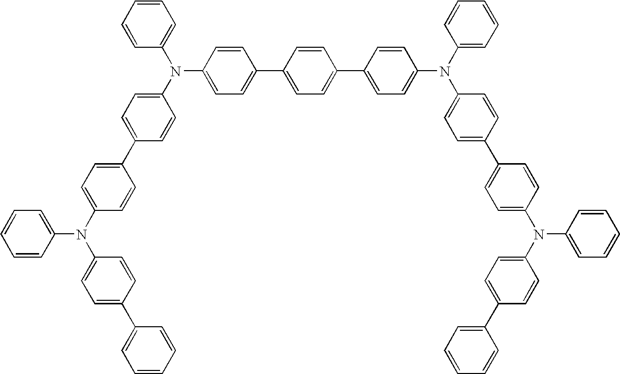
Appl. Phys. Lett. 90, 183503 (2007) 
Appl. Phys. Lett. 90, 183503 (2007) Triaylamine on spirofluorene core 
Synth. Met. 91, 209 (1997) Arylamine carbazole compounds 
Adv. Mater. 6, 677 (1994) Indolocarbazoles 
Synth. Met. 111, 421 (2000) Isoindole compounds 
Chem. Mater. 15, 3148 (2003) Phosphorescent OLED host materials Red hosts Arylcarbazoles 
Appl. Phys. Lett. 78, 1622 (2001) Metal 8-hydroxyquinolates (e.g., Alq3, BAlq) 
Nature 395, 151 (1998) 
US20060202194 
WO2005014551 Metal phenoxybenzothiazole compounds 
Appl. Phys. Lett. 90, 123509 (2007) Conjugated oligomers and polymers (e.g., polyfluorene) 
Org. Electron. 1, 15 (2000) Green hosts Arylcarbazoles 
Appl. Phys. Lett. 78, 1622 (2001) 
US2003175553 
WO2001039234 Aryltriphenylene compounds 
US20060280965 
US20060280965 Polymers (e.g., PVK) 
Appl. Phys. Lett. 77, 2280 (2000) Spirofluorene compounds 
WO2004093207 Metal phenoxybenzooxazole compounds 
WO05089025 
WO06132173 
JP200511610 Spirofluorene-carbazole compounds 
JP2007254297 
JP2007254297 Indolocabazoles 
WO07063796 
WO07063754 5-member ring electron deficient heterocycles (e.g., triazole, oxadiazole) 
J. Appl. Phys. 90, 5048 (2001) 
WO04107822 Metal phenoxypyridine compounds 
WO05030900 Blue hosts Arylcarbazoles 
Appl. Phys. Lett, 82, 2422 (2003) 
US20070190359 Dibenzothiophene- carbazole compounds 
WO2006114966 Phosphorescent dopants Red dopants Heavy metal porphyrins (e.g., PtOEP) 
Nature 395, 151 (1998) Iridium(III) organometallic complexes 
Appl. Phys. Lett. 78, 1622 (2001) 
US06835469 
US06835469 
US20060202194 
US20060202194 
US07087321 
US07087321 
Adv. Mater. 19, 739 (2007) Platinum(II) organometallic complexes 
WO2003040257 Osminum(III) complexes 
Chem. Mater. 17, 3532 (2005) Ruthenium(II) complexes 
Adv. Mater. 17, 1059 (2005) Green dopants Iridium(III) organometallic complexes 
Inorg. Chem. 40, 1704 (2001) 
US2002034656 
US06687266 
Chem. Mater. 16, 2480 (2004) 
US2007190359 
US 2006008670 JP2007123392 
Adv. Mater. 16, 2003 (2004) 
Angew. Chem. Int. Ed. 2006, 45, 7800 Pt(II) organometallic complexes 
Appl. Phys. Lett. 86, 153505 (2005) 
Appl. Phys. Lett. 86, 153505 (2005) 
Chem. Lett. 34, 592 (2005) Gold complexes 
Chem. Commun. 2906 (2005) Rhenium(III) complexes 
Inorg. Chem. 42, 1248 (2003) Blue dopants Iridium(III) organometallic complexes 
WO2002002714 
WO2006009024 
US2006251923 
WO2006056418, US2005260441 
US2007190359 
US2002134984 
Angew. Chem. Int. Ed. 47, 1 (2008) 
Chem. Mater. 18, 5119 (2006) 
Inorg. Chem. 46, 4308 (2007) 
WO05123873 
WO05123873 
WO07004380 
WO06082742 Osmium(II) complexes 
US2005260449 
Organometallics 23, 3745 (2004) Gold complexes 
Appl. Phys. Lett. 74, 1361 (1999) Platinum(II) complexes 
WO06098120, WO06103874 Exciton/hole blocking layer materials Bathocuprine compounds (e.g., BCP, BPhen) 
Appl. Phys. Lett. 75, 4 (1999) 
Appl. Phys. Lett. 79, 449 (2001) Metal 8-hydroxyquinolates (e.g., BAlq) 
Appl. Phys. Lett. 81, 162 (2002) 5-member ring electron deficient heterocycles such as triazole, oxadiazole, imidazole, benzoimidazole 
Appl. Phys. Lett. 81, 162 (2002) Triphenylene compounds 
US20050025993 Fluorinated aromatic compounds 
Appl. Phys. Lett. 79, 156 (2001) Electron transporting materials Anthracene- benzoimidazole compounds 
WO03060956 Anthracene-benzothiazole compounds 
Appl. Phys. Lett. 89, 063504 (2006) Metal 8-hydroxyquinolates (e.g., Alq3) 
Appl. Phys. Lett. 51, 913 (1987) Metal hydroxybenoquinolates 
Chem. Lett. 5, 905 (1993) Bathocuprine compounds such as BCP, BPhen, etc 
Appl. Phys. Lett. 91, 263503 (2007) 
Appl. Phys. Lett. 79, 449 (2001) 5-member ring electron deficient heterocycles (e.g.,triazole, oxadiazole, imidazole, benzoimidazole) 
Appl. Phys. Lett. 74, 865 (1999) 
Appl. Phys. Lett. 55, 1489 (1989) 
Jpn. J. Apply. Phys. 32, L917 (1993) Silole compounds 
Org. Electron. 4, 113 (2003) Arylborane compounds 
J. Am. Chem. Soc. 120, 9714 (1998) Fluorinated aromatic compounds 
J. Am. Chem. Soc. 122, 1832 (2000) - A number of devices were fabricated by thermal evaporation of the various layers layers, in sequence, on a commercially available ITO coated substrate. Table 2 shows the structure of various devices fabricated. Where a thickness appears at the head of a column, the layer corresponding to that column had that thickness in all devices. All concentrations are wt %, and where a concentration for a particular material is not specified, the material makes up the remainder of the material in the layer for which a concentration is not already specified, i.e., Device 1 has ITO/A (100 wt %)/A (99.5 wt %):B (0.5 wt %)/and so on.
-
TABLE 2 Device structures Device No. [10 nm] [20 nm] [15 nm] [40 nm] [90 nm] 1 ITO A A:B 0.5% C:E D LG201 LiF/Al [80 nm] 18% [5 nm] 2 ITO A A:B 1% C:E D LG201 LiF/Al [80 nm] 18% [5 nm] 3 ITO A A:B 1% C:E D LG201 LiF/Al [80 nm] 18% [5 nm] 4 ITO A A:B 0.5% C:E D LG201 LiF/Al [120 nm] 15% [5 nm] 5 ITO A A:B 0.5% C:E C LG201 LiF/Al [120 nm] 15% [5 nm] 6 ITO A A:B 0.5% C:E LG201 LiF/Al [120 nm] 15% 7 ITO A A:B 0.5% C:F D LG201 LiF/Al [120 nm] 18% [5 nm] 8 ITO A A:B 0.5% C:F C LG201 LiF/Al [120 nm] 18% [5 nm] 9 ITO A A:B 0.5% C:F LG201 LiF/Al [120 nm] 18% 10 ITO A A:B 0.5% D:F D LG201 LiF/Al [120 nm] 18% [5 nm] 11 ITO A A:B 0.5% D:F C LG201 LiF/Al [120 nm] 18% [5 nm] 12 ITO A A:B 0.5% D:F LG201 LiF/Al [120 nm] 18% 13 ITO A A:B 0.5% C:E D LG201 LiF/Al [80 nm] 15% [5 nm] 14 ITO A A:B 0.5% C:E C LG201 LiF/Al [80 nm] 15% [5 nm] 15 ITO A A:B 0.5% C:E LG201 LiF/Al [80 nm] 15% 16 ITO A A:B 0.5% C:F D LG201 LiF/Al [80 nm] 18% [5 nm] 17 ITO A A:B 0.5% C:F C LG201 LiF/Al [80 nm] 18% [5 nm] 18 ITO A A:B 0.5% C:F LG201 LiF/Al [80 nm] 18% 19 ITO A A:B 0.5% D:F D LG201 LiF/Al [80 nm] 18% [5 nm] 20 ITO A A:B 0.5% D:F C LG201 LiF/Al [80 nm] 18% [5 nm] 21 ITO A A:B 0.5% D:F LG201 LiF/Al [80 nm] 18% 22 ITO A A:B 0.5% C:E C LG201 LiF/Al [120 nm] 15% [5 nm] 23 ITO A A:B 0.5% C:E:A C LG201 LiF/Al [120 nm] 15%:0.5% [5 nm] 24 ITO A A:B 0.5% C:E:A C LG201 LiF/Al [120 nm] 15%:0.5% [5 nm] - Devices 25 and 26, which are not included in the table due to different layer thicknesses, had the following structures:
- Device 25: ITO(120 nm)/A(10 nm)/A:B[0.5%](20 nm)/mCBP:G [15%](15 nm)/mCBP(5 nm)/LG201(30 mm)/LiF/Al
- Device 26: ITO(120 nm)/H(30 nm)/NPD(10 nm)/A:B[0.5%](20 nm)/mCBP:G[15%](15 nm)/mCBP 5 nm)/LG201(30 nm)/LiF/Al
- Table 3 shows measured device performance characteristics for the devices described in Table 2. Voltage, luminous efficacy (in candelas per amp), external quantum efficiency, and power efficiency were measured at a luminance of 1000 nits. 1931 CIE coordinates were measured at a current density of 10 mA/cm2.
-
TABLE 3 Device Performance Characteristics At 1000 nits. At 10 mA/cm2 Luminous Power 1931 Voltage Efficacy EQE Efficiency 1931 CIE CIE Device No. [V] cd/A [%] [Lm/W] x y 1 4.5 33.1 16.7 22.9 0.442 0.443 2 4.5 33.8 17.8 23.6 0.456 0.434 3 4.5 25.7 13.2 17.9 0.437 0.445 4 4.3 34.3 16.1 25.3 0.416 0.429 5 5.0 17.4 8.1 10.8 0.407 0.429 6 5.1 6.4 3.0 4.0 0.402 0.427 7 4.3 43.3 18.8 31.4 0.424 0.475 8 4.7 31.8 13.7 21.3 0.415 0.476 9 4.5 15.4 6.4 10.6 0.388 0.487 10 4.8 28.7 13.7 18.9 0.473 0.450 11 5.1 21.2 10.2 13.1 0.480 0.447 12 4.5 20.5 9.5 14.4 0.455 0.456 13 4.3 32.4 17.0 23.7 0.395 0.395 14 5.1 17.4 9.0 10.8 0.379 0.393 15 5.2 7.0 3.6 4.2 0.378 0.391 16 4.6 36.0 17.3 24.5 0.414 0.454 17 5.1 29.9 14.1 18.4 0.396 0.455 18 4.8 18.3 8.6 12.0 0.393 0.456 19 5.2 21.0 10.7 12.6 0.444 0.438 20 5.6 18.4 9.4 10.3 0.450 0.437 21 4.9 16.8 8.5 10.8 0.442 0.439 22 4.6 10.7 5.1 7.3 0.422 0.423 23 4.6 11.7 5.0 7.9 0.423 0.463 24 4.5 14.3 5.5 9.9 0.402 0.493 25 4.9 16.7 9.3 10.6 0.280 0.310 26 5.3 14.9 8.3 8.7 0.323 0.322 - The measured device results show that devices having a combination of first emissive and non-emissive layers sharing a common first non-emissive material, and second emissive and non-emissive layer sharing a common second non-emissive material, show results unexepectedly superior to devices lacking the second non-emissive layer. All devices in Tables 2 and 3, with the exception of Device 26 which is a comparative example, have a first emissive layer that is 20 nm non-emitting Compound A doped with 0.5 wt % emitting Compound B, and a first non-emissive layer that is 10 nm of Compound A, where Compound A is the first non-emitting material that is common to the two layers. Some of the devices, specifically Device Nos. 5, 10, 14, 17, 19, 22, 23, and 24 also have a second emissive layer that is 15 nm of either non-emitting Compound C or D doped with emitting Compounds E, F and/or A, and a second non-emissive layer that is 5 nm of Compound C or D, where Compound C or D is the second non-emitting material that is common to the two layers. Other devices in the table use a non-emitting material in the second non-emissive layer that is different from the non-emitting material in the second emitting layer, or lack the second non-emissive layer.
- By comparing Device Nos. 5, 10, 14, 17 and 19 to Device Nos. 6, 12, 15, 18 and 21, respectively, it can be seen that the addition of a second non-emissive layer made of the same non-emitting material that is present in the second emissive layer dramatically improves device external quantum efficiency and power efficiency.
- It should also be noted that Compound D appears to be a better electron transport material than Compound C across various devices in Tables 2 and 3. The specific comparisons noted in the prior paragraph control for and remove effects caused by one specific material being better than another specific material, and isolate the effect caused by using a second non-emissive layer comprising the same non-emitting material as the second emissive layer.
- Comparing Device No. 25 and 26 shows that the use of a first non-emissive layer comprising a first non-emitting material, which is also used in an adjacent emissive layer comprising the first non-emitting material and a first emitting material, as in Device No. 25, may provide superior efficiency as compared to an otherwise identical device that uses a common hole-injection/hole transport material selection (Device No. 26).
- It is understood that the various embodiments described herein are by way of example only, and are not intended to limit the scope of the invention. For example, many of the materials and structures described herein may be substituted with other materials and structures without deviating from the spirit of the invention. The present invention as claimed may therefore includes variations from the particular examples and preferred embodiments described herein, as will be apparent to one of skill in the art. It is understood that various theories as to why the invention works are not intended to be limiting.
Claims (12)
Priority Applications (3)
| Application Number | Priority Date | Filing Date | Title |
|---|---|---|---|
| US12/332,945 US8040053B2 (en) | 2008-02-09 | 2008-12-11 | Organic light emitting device architecture for reducing the number of organic materials |
| PCT/US2009/030545 WO2009099705A1 (en) | 2008-02-09 | 2009-01-09 | Organic licht emitting device with a non-emissive organometallic layer |
| TW098102101A TWI527498B (en) | 2008-02-09 | 2009-01-20 | Organic light emitting device architecture |
Applications Claiming Priority (2)
| Application Number | Priority Date | Filing Date | Title |
|---|---|---|---|
| US6513108P | 2008-02-09 | 2008-02-09 | |
| US12/332,945 US8040053B2 (en) | 2008-02-09 | 2008-12-11 | Organic light emitting device architecture for reducing the number of organic materials |
Publications (2)
| Publication Number | Publication Date |
|---|---|
| US20090200927A1 true US20090200927A1 (en) | 2009-08-13 |
| US8040053B2 US8040053B2 (en) | 2011-10-18 |
Family
ID=40938329
Family Applications (1)
| Application Number | Title | Priority Date | Filing Date |
|---|---|---|---|
| US12/332,945 Active 2029-07-07 US8040053B2 (en) | 2008-02-09 | 2008-12-11 | Organic light emitting device architecture for reducing the number of organic materials |
Country Status (3)
| Country | Link |
|---|---|
| US (1) | US8040053B2 (en) |
| TW (1) | TWI527498B (en) |
| WO (1) | WO2009099705A1 (en) |
Cited By (12)
| Publication number | Priority date | Publication date | Assignee | Title |
|---|---|---|---|---|
| JP2010141008A (en) * | 2008-12-10 | 2010-06-24 | Konica Minolta Holdings Inc | Organic electroluminescent element, organic electroluminescent element material, display device, and lighting device |
| US20110057559A1 (en) * | 2007-12-28 | 2011-03-10 | Universal Display Corporation | Phosphorescent emitters and host materials with improved stability |
| US20110204333A1 (en) * | 2010-02-25 | 2011-08-25 | Universal Display Corporation | Phosphorescent emitters |
| US20120049166A1 (en) * | 2010-08-25 | 2012-03-01 | National Tsing Hua University | Organic light emitting diode |
| US20120267618A1 (en) * | 2009-10-05 | 2012-10-25 | Thorn Lighting Ltd. | Multilayer Organic Device |
| WO2013058087A1 (en) * | 2011-10-21 | 2013-04-25 | コニカミノルタ株式会社 | Organic electroluminscent element |
| US8604689B2 (en) | 2010-11-11 | 2013-12-10 | Nitto Denko Corporation | Hybrid composite emissive construct and light-emitting devices using the same |
| US8790794B2 (en) | 2010-09-09 | 2014-07-29 | Semiconductor Energy Laboratory Co., Ltd. | Heterocyclic compound, light-emitting element, light-emitting device, electronic device, and lighting device |
| US8933439B2 (en) | 2010-02-05 | 2015-01-13 | Nitto Denko Corporation | Organic light-emitting diode with enhanced efficiency |
| US20150076465A1 (en) * | 2012-04-23 | 2015-03-19 | E I Du Pont De Nemours And Company | Blue luminescent compounds |
| JPWO2013094276A1 (en) * | 2011-12-20 | 2015-04-27 | コニカミノルタ株式会社 | Organic EL device |
| US20210159282A1 (en) * | 2014-12-08 | 2021-05-27 | Lg Display Co., Ltd. | Organic light emitting display device |
Families Citing this family (4)
| Publication number | Priority date | Publication date | Assignee | Title |
|---|---|---|---|---|
| JP6675193B2 (en) * | 2011-03-31 | 2020-04-01 | ユー・ディー・シー アイルランド リミテッド | Host material of organic electroluminescent device, organic electroluminescent device, light emitting device, display device, and lighting device |
| CA2890253A1 (en) | 2012-11-06 | 2014-05-15 | Oti Lumionics Inc. | Method for depositing a conductive coating on a surface |
| CN108431981B (en) | 2015-12-16 | 2022-05-24 | Oti领英有限公司 | Barrier coatings for optoelectronic devices |
| WO2018033860A1 (en) | 2016-08-15 | 2018-02-22 | Oti Lumionics Inc. | Light transmissive electrode for light emitting devices |
Citations (49)
| Publication number | Priority date | Publication date | Assignee | Title |
|---|---|---|---|---|
| US700938A (en) * | 1902-03-01 | 1902-05-27 | Robert W Johnson | Bandage. |
| US4769292A (en) * | 1987-03-02 | 1988-09-06 | Eastman Kodak Company | Electroluminescent device with modified thin film luminescent zone |
| US5061569A (en) * | 1990-07-26 | 1991-10-29 | Eastman Kodak Company | Electroluminescent device with organic electroluminescent medium |
| US5247190A (en) * | 1989-04-20 | 1993-09-21 | Cambridge Research And Innovation Limited | Electroluminescent devices |
| US5703436A (en) * | 1994-12-13 | 1997-12-30 | The Trustees Of Princeton University | Transparent contacts for organic devices |
| US5707745A (en) * | 1994-12-13 | 1998-01-13 | The Trustees Of Princeton University | Multicolor organic light emitting devices |
| US5834893A (en) * | 1996-12-23 | 1998-11-10 | The Trustees Of Princeton University | High efficiency organic light emitting devices with light directing structures |
| US5844363A (en) * | 1997-01-23 | 1998-12-01 | The Trustees Of Princeton Univ. | Vacuum deposited, non-polymeric flexible organic light emitting devices |
| US6013982A (en) * | 1996-12-23 | 2000-01-11 | The Trustees Of Princeton University | Multicolor display devices |
| US6087196A (en) * | 1998-01-30 | 2000-07-11 | The Trustees Of Princeton University | Fabrication of organic semiconductor devices using ink jet printing |
| US6091195A (en) * | 1997-02-03 | 2000-07-18 | The Trustees Of Princeton University | Displays having mesa pixel configuration |
| US6097147A (en) * | 1998-09-14 | 2000-08-01 | The Trustees Of Princeton University | Structure for high efficiency electroluminescent device |
| US6294398B1 (en) * | 1999-11-23 | 2001-09-25 | The Trustees Of Princeton University | Method for patterning devices |
| US6303238B1 (en) * | 1997-12-01 | 2001-10-16 | The Trustees Of Princeton University | OLEDs doped with phosphorescent compounds |
| US6337102B1 (en) * | 1997-11-17 | 2002-01-08 | The Trustees Of Princeton University | Low pressure vapor phase deposition of organic thin films |
| US20020034656A1 (en) * | 1998-09-14 | 2002-03-21 | Thompson Mark E. | Organometallic complexes as phosphorescent emitters in organic LEDs |
| US20020134984A1 (en) * | 2001-02-01 | 2002-09-26 | Fuji Photo Film Co., Ltd. | Transition metal complex and light-emitting device |
| US20030175553A1 (en) * | 2001-12-28 | 2003-09-18 | Thompson Mark E. | White light emitting oleds from combined monomer and aggregate emission |
| US20030230980A1 (en) * | 2002-06-18 | 2003-12-18 | Forrest Stephen R | Very low voltage, high efficiency phosphorescent oled in a p-i-n structure |
| US6687266B1 (en) * | 2002-11-08 | 2004-02-03 | Universal Display Corporation | Organic light emitting materials and devices |
| US20040174116A1 (en) * | 2001-08-20 | 2004-09-09 | Lu Min-Hao Michael | Transparent electrodes |
| US6835469B2 (en) * | 2001-10-17 | 2004-12-28 | The University Of Southern California | Phosphorescent compounds and devices comprising the same |
| US20050025993A1 (en) * | 2003-07-25 | 2005-02-03 | Thompson Mark E. | Materials and structures for enhancing the performance of organic light emitting devices |
| US20050046337A1 (en) * | 2003-09-03 | 2005-03-03 | Byung-Doo Chin | Organic lights-emitting device with doped emission layer |
| US6869695B2 (en) * | 2001-12-28 | 2005-03-22 | The Trustees Of Princeton University | White light emitting OLEDs from combined monomer and aggregate emission |
| US20050074630A1 (en) * | 2003-03-27 | 2005-04-07 | Hiroshi Kanno | Organic electroluminescent device |
| US20050077817A1 (en) * | 2002-12-26 | 2005-04-14 | Semiconductor Energy Laboratory Co., Ltd. | Organic light emitting element and a light emitting device using the same |
| US20050260441A1 (en) * | 2004-05-18 | 2005-11-24 | Thompson Mark E | Luminescent compounds with carbene ligands |
| US20050260449A1 (en) * | 2004-05-18 | 2005-11-24 | Robert Walters | Complexes with tridentate ligands |
| US20060008670A1 (en) * | 2004-07-06 | 2006-01-12 | Chun Lin | Organic light emitting materials and devices |
| US20060046096A1 (en) * | 2004-08-25 | 2006-03-02 | Semiconductor Energy Laboratory Co., Ltd. | Light emitting element and light emitting device using the same |
| US7022421B2 (en) * | 2001-08-29 | 2006-04-04 | The University Of Southern California | Organic light emitting devices having carrier blocking layers comprising metal complexes |
| US20060125380A1 (en) * | 2004-12-13 | 2006-06-15 | Yoshiaki Nagara | Organic EL devices |
| US20060141288A1 (en) * | 2001-05-24 | 2006-06-29 | Idemitsu Kosan Co., Ltd. | Organic electroluminescence element |
| US7078113B2 (en) * | 2001-08-29 | 2006-07-18 | The University Of Southern California | Organic light emitting devices having carrier transporting layers comprising metal complexes |
| US7087321B2 (en) * | 2003-04-22 | 2006-08-08 | Universal Display Corporation | Organic light emitting devices having reduced pixel shrinkage |
| US20060202194A1 (en) * | 2005-03-08 | 2006-09-14 | Jeong Hyun C | Red phosphorescene compounds and organic electroluminescence device using the same |
| US20060232194A1 (en) * | 2005-04-13 | 2006-10-19 | Yeh-Jiun Tung | Hybrid OLED having phosphorescent and fluorescent emitters |
| US20060251923A1 (en) * | 2005-05-06 | 2006-11-09 | Chun Lin | Stability OLED materials and devices |
| US7151339B2 (en) * | 2004-01-30 | 2006-12-19 | Universal Display Corporation | OLED efficiency by utilization of different doping concentrations within the device emissive layer |
| US20070190359A1 (en) * | 2006-02-10 | 2007-08-16 | Knowles David B | Metal complexes of cyclometallated imidazo[1,2-ƒ]phenanthridine and diimidazo[1,2-a:1',2'-c]quinazoline ligands and isoelectronic and benzannulated analogs thereof |
| US7285907B2 (en) * | 2001-05-16 | 2007-10-23 | The University Of Southern California | High efficiency multi-color electro-phosphorescent OLEDs |
| US7294849B2 (en) * | 2001-03-14 | 2007-11-13 | The Trustees Of Princeton University | Materials and devices for blue phosphorescence based organic light emitting diodes |
| US7431968B1 (en) * | 2001-09-04 | 2008-10-07 | The Trustees Of Princeton University | Process and apparatus for organic vapor jet deposition |
| US7466073B2 (en) * | 2004-09-29 | 2008-12-16 | Canon Kabushiki Kaisha | Organic electroluminescent device and display apparatus |
| US7714498B2 (en) * | 2004-06-07 | 2010-05-11 | Panasonic Corporation | Electroluminescent device with acetylacetonato complex salt included in phosphor layer |
| US7768195B2 (en) * | 2006-05-25 | 2010-08-03 | Idemitsu Kosan Co., Ltd. | Organic electroluminescent device with improved luminous efficiency |
| US7862906B2 (en) * | 2003-04-09 | 2011-01-04 | Semiconductor Energy Laboratory Co., Ltd. | Electroluminescent element and light-emitting device |
| US7871711B2 (en) * | 2004-03-31 | 2011-01-18 | Fujifilm Corporation | Organic electroluminescent element and organic electroluminescent display |
Family Cites Families (30)
| Publication number | Priority date | Publication date | Assignee | Title |
|---|---|---|---|---|
| DE69412567T2 (en) | 1993-11-01 | 1999-02-04 | Hodogaya Chemical Co Ltd | Amine compound and electroluminescent device containing it |
| US6458475B1 (en) | 1999-11-24 | 2002-10-01 | The Trustee Of Princeton University | Organic light emitting diode having a blue phosphorescent molecule as an emitter |
| US6660410B2 (en) | 2000-03-27 | 2003-12-09 | Idemitsu Kosan Co., Ltd. | Organic electroluminescence element |
| US20020121638A1 (en) | 2000-06-30 | 2002-09-05 | Vladimir Grushin | Electroluminescent iridium compounds with fluorinated phenylpyridines, phenylpyrimidines, and phenylquinolines and devices made with such compounds |
| US7166368B2 (en) | 2001-11-07 | 2007-01-23 | E. I. Du Pont De Nemours And Company | Electroluminescent platinum compounds and devices made with such compounds |
| KR100691543B1 (en) | 2002-01-18 | 2007-03-09 | 주식회사 엘지화학 | New material for transporting electron and organic electroluminescent display using the same |
| JP3786023B2 (en) | 2002-01-31 | 2006-06-14 | 株式会社豊田自動織機 | Organic EL device |
| EP1589789B1 (en) | 2003-01-24 | 2015-07-01 | Idemitsu Kosan Co., Ltd. | Organic electroluminescence device |
| EP1717291A3 (en) | 2003-04-15 | 2007-03-21 | Merck Patent GmbH | Mixtures of matrix materials and organic semiconductors capable of emission, use of the same and electronic components containing said mixtures |
| US20060186791A1 (en) | 2003-05-29 | 2006-08-24 | Osamu Yoshitake | Organic electroluminescent element |
| JP2005011610A (en) | 2003-06-18 | 2005-01-13 | Nippon Steel Chem Co Ltd | Organic electroluminescent element |
| JP4899284B2 (en) | 2003-07-18 | 2012-03-21 | コニカミノルタホールディングス株式会社 | Organic electroluminescence element, lighting device and display device |
| TWI390006B (en) | 2003-08-07 | 2013-03-21 | Nippon Steel Chemical Co | Organic EL materials with aluminum clamps |
| US20060269780A1 (en) | 2003-09-25 | 2006-11-30 | Takayuki Fukumatsu | Organic electroluminescent device |
| TW200531592A (en) | 2004-03-15 | 2005-09-16 | Nippon Steel Chemical Co | Organic electroluminescent device |
| WO2005123873A1 (en) | 2004-06-17 | 2005-12-29 | Konica Minolta Holdings, Inc. | Organic electroluminescent device material, organic electroluminescent device, display and illuminating device |
| EP2178348B1 (en) | 2004-07-23 | 2012-11-21 | Konica Minolta Holdings, Inc. | Organic electroluminescent element, display and illuminator |
| DE102004057072A1 (en) | 2004-11-25 | 2006-06-01 | Basf Ag | Use of Transition Metal Carbene Complexes in Organic Light Emitting Diodes (OLEDs) |
| US8377571B2 (en) | 2005-02-04 | 2013-02-19 | Konica Minolta Holdings, Inc. | Material for organic electroluminescence element, organic electroluminescence element, display device and lighting device |
| JP5125502B2 (en) | 2005-03-16 | 2013-01-23 | コニカミノルタホールディングス株式会社 | Organic electroluminescence element material, organic electroluminescence element |
| WO2006103874A1 (en) | 2005-03-29 | 2006-10-05 | Konica Minolta Holdings, Inc. | Organic electroluminescent device material, organic electroluminescent device, display and illuminating device |
| US8231983B2 (en) | 2005-04-18 | 2012-07-31 | Konica Minolta Holdings Inc. | Organic electroluminescent device, display and illuminating device |
| KR101010846B1 (en) | 2005-06-07 | 2011-01-25 | 신닛테츠가가쿠 가부시키가이샤 | Organic metal complex and organic electroluminescent device using same |
| JP5076891B2 (en) | 2005-07-01 | 2012-11-21 | コニカミノルタホールディングス株式会社 | ORGANIC ELECTROLUMINESCENT ELEMENT MATERIAL, ORGANIC ELECTROLUMINESCENT ELEMENT, DISPLAY DEVICE AND LIGHTING DEVICE |
| JP4887731B2 (en) | 2005-10-26 | 2012-02-29 | コニカミノルタホールディングス株式会社 | Organic electroluminescence element, display device and lighting device |
| KR20080085000A (en) | 2005-12-01 | 2008-09-22 | 신닛테츠가가쿠 가부시키가이샤 | Organic electroluminescent device |
| CN102633820B (en) | 2005-12-01 | 2015-01-21 | 新日铁住金化学株式会社 | Compound for organic electroluminescent element and organic electroluminescent element |
| JP4823730B2 (en) | 2006-03-20 | 2011-11-24 | 新日鐵化学株式会社 | Luminescent layer compound and organic electroluminescent device |
| EP2097938B1 (en) | 2006-12-28 | 2019-07-17 | Universal Display Corporation | Long lifetime phosphorescent organic light emitting device (oled) structures |
| CN102203977B (en) | 2008-09-04 | 2014-06-04 | 通用显示公司 | White phosphorescent organic light emitting devices |
-
2008
- 2008-12-11 US US12/332,945 patent/US8040053B2/en active Active
-
2009
- 2009-01-09 WO PCT/US2009/030545 patent/WO2009099705A1/en active Application Filing
- 2009-01-20 TW TW098102101A patent/TWI527498B/en active
Patent Citations (52)
| Publication number | Priority date | Publication date | Assignee | Title |
|---|---|---|---|---|
| US700938A (en) * | 1902-03-01 | 1902-05-27 | Robert W Johnson | Bandage. |
| US4769292A (en) * | 1987-03-02 | 1988-09-06 | Eastman Kodak Company | Electroluminescent device with modified thin film luminescent zone |
| US5247190A (en) * | 1989-04-20 | 1993-09-21 | Cambridge Research And Innovation Limited | Electroluminescent devices |
| US5061569A (en) * | 1990-07-26 | 1991-10-29 | Eastman Kodak Company | Electroluminescent device with organic electroluminescent medium |
| US5703436A (en) * | 1994-12-13 | 1997-12-30 | The Trustees Of Princeton University | Transparent contacts for organic devices |
| US5707745A (en) * | 1994-12-13 | 1998-01-13 | The Trustees Of Princeton University | Multicolor organic light emitting devices |
| US5834893A (en) * | 1996-12-23 | 1998-11-10 | The Trustees Of Princeton University | High efficiency organic light emitting devices with light directing structures |
| US6013982A (en) * | 1996-12-23 | 2000-01-11 | The Trustees Of Princeton University | Multicolor display devices |
| US5844363A (en) * | 1997-01-23 | 1998-12-01 | The Trustees Of Princeton Univ. | Vacuum deposited, non-polymeric flexible organic light emitting devices |
| US6091195A (en) * | 1997-02-03 | 2000-07-18 | The Trustees Of Princeton University | Displays having mesa pixel configuration |
| US6337102B1 (en) * | 1997-11-17 | 2002-01-08 | The Trustees Of Princeton University | Low pressure vapor phase deposition of organic thin films |
| US6303238B1 (en) * | 1997-12-01 | 2001-10-16 | The Trustees Of Princeton University | OLEDs doped with phosphorescent compounds |
| US6087196A (en) * | 1998-01-30 | 2000-07-11 | The Trustees Of Princeton University | Fabrication of organic semiconductor devices using ink jet printing |
| US20020034656A1 (en) * | 1998-09-14 | 2002-03-21 | Thompson Mark E. | Organometallic complexes as phosphorescent emitters in organic LEDs |
| US6097147A (en) * | 1998-09-14 | 2000-08-01 | The Trustees Of Princeton University | Structure for high efficiency electroluminescent device |
| US6468819B1 (en) * | 1999-11-23 | 2002-10-22 | The Trustees Of Princeton University | Method for patterning organic thin film devices using a die |
| US6294398B1 (en) * | 1999-11-23 | 2001-09-25 | The Trustees Of Princeton University | Method for patterning devices |
| US20020134984A1 (en) * | 2001-02-01 | 2002-09-26 | Fuji Photo Film Co., Ltd. | Transition metal complex and light-emitting device |
| US7294849B2 (en) * | 2001-03-14 | 2007-11-13 | The Trustees Of Princeton University | Materials and devices for blue phosphorescence based organic light emitting diodes |
| US7285907B2 (en) * | 2001-05-16 | 2007-10-23 | The University Of Southern California | High efficiency multi-color electro-phosphorescent OLEDs |
| US20060141288A1 (en) * | 2001-05-24 | 2006-06-29 | Idemitsu Kosan Co., Ltd. | Organic electroluminescence element |
| US20040174116A1 (en) * | 2001-08-20 | 2004-09-09 | Lu Min-Hao Michael | Transparent electrodes |
| US7078113B2 (en) * | 2001-08-29 | 2006-07-18 | The University Of Southern California | Organic light emitting devices having carrier transporting layers comprising metal complexes |
| US7022421B2 (en) * | 2001-08-29 | 2006-04-04 | The University Of Southern California | Organic light emitting devices having carrier blocking layers comprising metal complexes |
| US7431968B1 (en) * | 2001-09-04 | 2008-10-07 | The Trustees Of Princeton University | Process and apparatus for organic vapor jet deposition |
| US6835469B2 (en) * | 2001-10-17 | 2004-12-28 | The University Of Southern California | Phosphorescent compounds and devices comprising the same |
| US6869695B2 (en) * | 2001-12-28 | 2005-03-22 | The Trustees Of Princeton University | White light emitting OLEDs from combined monomer and aggregate emission |
| US20030175553A1 (en) * | 2001-12-28 | 2003-09-18 | Thompson Mark E. | White light emitting oleds from combined monomer and aggregate emission |
| US20030230980A1 (en) * | 2002-06-18 | 2003-12-18 | Forrest Stephen R | Very low voltage, high efficiency phosphorescent oled in a p-i-n structure |
| US6687266B1 (en) * | 2002-11-08 | 2004-02-03 | Universal Display Corporation | Organic light emitting materials and devices |
| US20050077817A1 (en) * | 2002-12-26 | 2005-04-14 | Semiconductor Energy Laboratory Co., Ltd. | Organic light emitting element and a light emitting device using the same |
| US20050074630A1 (en) * | 2003-03-27 | 2005-04-07 | Hiroshi Kanno | Organic electroluminescent device |
| US7611779B2 (en) * | 2003-03-27 | 2009-11-03 | Sanyo Electric Co., Ltd. | Organic electroluminescent device |
| US7862906B2 (en) * | 2003-04-09 | 2011-01-04 | Semiconductor Energy Laboratory Co., Ltd. | Electroluminescent element and light-emitting device |
| US7087321B2 (en) * | 2003-04-22 | 2006-08-08 | Universal Display Corporation | Organic light emitting devices having reduced pixel shrinkage |
| US20050025993A1 (en) * | 2003-07-25 | 2005-02-03 | Thompson Mark E. | Materials and structures for enhancing the performance of organic light emitting devices |
| US20050046337A1 (en) * | 2003-09-03 | 2005-03-03 | Byung-Doo Chin | Organic lights-emitting device with doped emission layer |
| US7151339B2 (en) * | 2004-01-30 | 2006-12-19 | Universal Display Corporation | OLED efficiency by utilization of different doping concentrations within the device emissive layer |
| US7871711B2 (en) * | 2004-03-31 | 2011-01-18 | Fujifilm Corporation | Organic electroluminescent element and organic electroluminescent display |
| US20050260441A1 (en) * | 2004-05-18 | 2005-11-24 | Thompson Mark E | Luminescent compounds with carbene ligands |
| US20050260449A1 (en) * | 2004-05-18 | 2005-11-24 | Robert Walters | Complexes with tridentate ligands |
| US7279704B2 (en) * | 2004-05-18 | 2007-10-09 | The University Of Southern California | Complexes with tridentate ligands |
| US7714498B2 (en) * | 2004-06-07 | 2010-05-11 | Panasonic Corporation | Electroluminescent device with acetylacetonato complex salt included in phosphor layer |
| US20060008670A1 (en) * | 2004-07-06 | 2006-01-12 | Chun Lin | Organic light emitting materials and devices |
| US20060046096A1 (en) * | 2004-08-25 | 2006-03-02 | Semiconductor Energy Laboratory Co., Ltd. | Light emitting element and light emitting device using the same |
| US7466073B2 (en) * | 2004-09-29 | 2008-12-16 | Canon Kabushiki Kaisha | Organic electroluminescent device and display apparatus |
| US20060125380A1 (en) * | 2004-12-13 | 2006-06-15 | Yoshiaki Nagara | Organic EL devices |
| US20060202194A1 (en) * | 2005-03-08 | 2006-09-14 | Jeong Hyun C | Red phosphorescene compounds and organic electroluminescence device using the same |
| US20060232194A1 (en) * | 2005-04-13 | 2006-10-19 | Yeh-Jiun Tung | Hybrid OLED having phosphorescent and fluorescent emitters |
| US20060251923A1 (en) * | 2005-05-06 | 2006-11-09 | Chun Lin | Stability OLED materials and devices |
| US20070190359A1 (en) * | 2006-02-10 | 2007-08-16 | Knowles David B | Metal complexes of cyclometallated imidazo[1,2-ƒ]phenanthridine and diimidazo[1,2-a:1',2'-c]quinazoline ligands and isoelectronic and benzannulated analogs thereof |
| US7768195B2 (en) * | 2006-05-25 | 2010-08-03 | Idemitsu Kosan Co., Ltd. | Organic electroluminescent device with improved luminous efficiency |
Cited By (21)
| Publication number | Priority date | Publication date | Assignee | Title |
|---|---|---|---|---|
| US20110057559A1 (en) * | 2007-12-28 | 2011-03-10 | Universal Display Corporation | Phosphorescent emitters and host materials with improved stability |
| US8586204B2 (en) | 2007-12-28 | 2013-11-19 | Universal Display Corporation | Phosphorescent emitters and host materials with improved stability |
| JP2010141008A (en) * | 2008-12-10 | 2010-06-24 | Konica Minolta Holdings Inc | Organic electroluminescent element, organic electroluminescent element material, display device, and lighting device |
| US20120267618A1 (en) * | 2009-10-05 | 2012-10-25 | Thorn Lighting Ltd. | Multilayer Organic Device |
| US9054317B2 (en) * | 2009-10-05 | 2015-06-09 | Thorn Lighting Ltd. | Multilayer organic device |
| US8933439B2 (en) | 2010-02-05 | 2015-01-13 | Nitto Denko Corporation | Organic light-emitting diode with enhanced efficiency |
| US9601710B2 (en) | 2010-02-05 | 2017-03-21 | Nitto Denko Corporation | Organic light-emitting diode with enhanced efficiency |
| US20110204333A1 (en) * | 2010-02-25 | 2011-08-25 | Universal Display Corporation | Phosphorescent emitters |
| US9156870B2 (en) | 2010-02-25 | 2015-10-13 | Universal Display Corporation | Phosphorescent emitters |
| WO2011106344A1 (en) * | 2010-02-25 | 2011-09-01 | Universal Display Corporation | Phosphorescent emitters |
| US20120049166A1 (en) * | 2010-08-25 | 2012-03-01 | National Tsing Hua University | Organic light emitting diode |
| US8790794B2 (en) | 2010-09-09 | 2014-07-29 | Semiconductor Energy Laboratory Co., Ltd. | Heterocyclic compound, light-emitting element, light-emitting device, electronic device, and lighting device |
| US9406893B2 (en) | 2010-09-09 | 2016-08-02 | Semiconductor Energy Laboratory Co., Ltd. | Heterocyclic compound, light-emitting element, light-emitting device, electronic device, and lighting device |
| US8604689B2 (en) | 2010-11-11 | 2013-12-10 | Nitto Denko Corporation | Hybrid composite emissive construct and light-emitting devices using the same |
| JPWO2013058087A1 (en) * | 2011-10-21 | 2015-04-02 | コニカミノルタ株式会社 | Organic electroluminescence device |
| WO2013058087A1 (en) * | 2011-10-21 | 2013-04-25 | コニカミノルタ株式会社 | Organic electroluminscent element |
| JPWO2013094276A1 (en) * | 2011-12-20 | 2015-04-27 | コニカミノルタ株式会社 | Organic EL device |
| US20150076465A1 (en) * | 2012-04-23 | 2015-03-19 | E I Du Pont De Nemours And Company | Blue luminescent compounds |
| US9685618B2 (en) * | 2012-04-23 | 2017-06-20 | E I Du Pont De Nemours And Company | Blue luminescent compounds |
| US20210159282A1 (en) * | 2014-12-08 | 2021-05-27 | Lg Display Co., Ltd. | Organic light emitting display device |
| US11770955B2 (en) * | 2014-12-08 | 2023-09-26 | Lg Display Co., Ltd. | Organic light emitting display device |
Also Published As
| Publication number | Publication date |
|---|---|
| TW200948183A (en) | 2009-11-16 |
| TWI527498B (en) | 2016-03-21 |
| US8040053B2 (en) | 2011-10-18 |
| WO2009099705A1 (en) | 2009-08-13 |
Similar Documents
| Publication | Publication Date | Title |
|---|---|---|
| US8040053B2 (en) | Organic light emitting device architecture for reducing the number of organic materials | |
| US11716902B2 (en) | Organic electroluminescent materials and devices | |
| US11871652B2 (en) | Organic electroluminescent materials and devices | |
| US11289659B2 (en) | Organic electroluminescent materials and devices | |
| US8053770B2 (en) | Emissive layer patterning for OLED | |
| US8778511B2 (en) | OLED stability via doped hole transport layer | |
| US8367223B2 (en) | Heteroleptic phosphorescent emitters | |
| US8513658B2 (en) | White phosphorescent organic light emitting devices | |
| US11696459B2 (en) | Phosphorescence-sensitized delayed fluorescence light emitting system | |
| US9142791B2 (en) | OLED having multi-component emissive layer | |
| US9670404B2 (en) | Organic electroluminescent materials and devices | |
| US9773985B2 (en) | Organic electroluminescent materials and devices | |
| US20140131665A1 (en) | Organic Electroluminescent Device With Delayed Fluorescence | |
| US20150295197A1 (en) | Efficient Organic Electroluminescent Devices | |
| US9450198B2 (en) | Organic electroluminescent materials and devices | |
| US8372526B2 (en) | Intermediate connector for stacked organic light emitting devices | |
| US9287513B2 (en) | Organic electroluminescent materials and devices | |
| US10147892B2 (en) | Organic electroluminescent materials and devices | |
| US20240147834A1 (en) | Organic electroluminescent materials and devices |
Legal Events
| Date | Code | Title | Description |
|---|---|---|---|
| AS | Assignment |
Owner name: UNIVERSAL DISPLAY CORPORATION, NEW JERSEY Free format text: ASSIGNMENT OF ASSIGNORS INTEREST;ASSIGNORS:D'ANDRADE, BRIAN;ESLER, JAMES;REEL/FRAME:022589/0498;SIGNING DATES FROM 20090301 TO 20090323 Owner name: UNIVERSAL DISPLAY CORPORATION, NEW JERSEY Free format text: ASSIGNMENT OF ASSIGNORS INTEREST;ASSIGNORS:D'ANDRADE, BRIAN;ESLER, JAMES;SIGNING DATES FROM 20090301 TO 20090323;REEL/FRAME:022589/0498 |
|
| STCF | Information on status: patent grant |
Free format text: PATENTED CASE |
|
| FEPP | Fee payment procedure |
Free format text: PAYOR NUMBER ASSIGNED (ORIGINAL EVENT CODE: ASPN); ENTITY STATUS OF PATENT OWNER: LARGE ENTITY Free format text: PAYER NUMBER DE-ASSIGNED (ORIGINAL EVENT CODE: RMPN); ENTITY STATUS OF PATENT OWNER: LARGE ENTITY |
|
| FPAY | Fee payment |
Year of fee payment: 4 |
|
| MAFP | Maintenance fee payment |
Free format text: PAYMENT OF MAINTENANCE FEE, 8TH YEAR, LARGE ENTITY (ORIGINAL EVENT CODE: M1552); ENTITY STATUS OF PATENT OWNER: LARGE ENTITY Year of fee payment: 8 |
|
| MAFP | Maintenance fee payment |
Free format text: PAYMENT OF MAINTENANCE FEE, 12TH YEAR, LARGE ENTITY (ORIGINAL EVENT CODE: M1553); ENTITY STATUS OF PATENT OWNER: LARGE ENTITY Year of fee payment: 12 |