US20100090591A1 - Phosphorescent materials - Google Patents
Phosphorescent materials Download PDFInfo
- Publication number
- US20100090591A1 US20100090591A1 US12/559,764 US55976409A US2010090591A1 US 20100090591 A1 US20100090591 A1 US 20100090591A1 US 55976409 A US55976409 A US 55976409A US 2010090591 A1 US2010090591 A1 US 2010090591A1
- Authority
- US
- United States
- Prior art keywords
- compound
- group
- metal
- host
- ring
- Prior art date
- Legal status (The legal status is an assumption and is not a legal conclusion. Google has not performed a legal analysis and makes no representation as to the accuracy of the status listed.)
- Granted
Links
- 0 *.B.CC.CC1=OC(C)(N)OC(C)=C1C.C[RaH].C[Rb] Chemical compound *.B.CC.CC1=OC(C)(N)OC(C)=C1C.C[RaH].C[Rb] 0.000 description 10
- JHHICJNNBNUFMW-BVIFHCHWSA-J CC1=CC(C)=C2C(=C1)C1=N(C3=C(C=CC(CC(C)C)=C3)C=C1)[Ir]21OC(C)=C(C)C(C)=O1.CC1=CC(C)=C2C(=C1)C1=N(C3=C(C=CC=C3)C=C1)[Ir]21OC(C)=C(C)C(C)=O1.CC1=CC(C)=C2C(=C1)C1=N(C3=C(C=CC=C3)C=C1C)[Ir]21OC(C)=CC(C)=O1.CC1=CC(C)=O[Ir]2(O1)C1=C(CC(C)C)C=C(CC(C)C)C=C1C1=N2C2=C(C=CC=C2)C=C1 Chemical compound CC1=CC(C)=C2C(=C1)C1=N(C3=C(C=CC(CC(C)C)=C3)C=C1)[Ir]21OC(C)=C(C)C(C)=O1.CC1=CC(C)=C2C(=C1)C1=N(C3=C(C=CC=C3)C=C1)[Ir]21OC(C)=C(C)C(C)=O1.CC1=CC(C)=C2C(=C1)C1=N(C3=C(C=CC=C3)C=C1C)[Ir]21OC(C)=CC(C)=O1.CC1=CC(C)=O[Ir]2(O1)C1=C(CC(C)C)C=C(CC(C)C)C=C1C1=N2C2=C(C=CC=C2)C=C1 JHHICJNNBNUFMW-BVIFHCHWSA-J 0.000 description 8
- GSOHKPVFCOWKPU-UHFFFAOYSA-N CC(=O)C(C)C(C)=O Chemical compound CC(=O)C(C)C(C)=O GSOHKPVFCOWKPU-UHFFFAOYSA-N 0.000 description 7
- NIMAVDVPQOMPKC-UHFFFAOYSA-N B.CC.CC1=OC(C)(N)OC(C)=C1C.C[RaH].C[Rb] Chemical compound B.CC.CC1=OC(C)(N)OC(C)=C1C.C[RaH].C[Rb] NIMAVDVPQOMPKC-UHFFFAOYSA-N 0.000 description 6
- OBXVHVJYVIJWJO-IWOQRIGNSA-J CC1=CC(C)=C2C(=C1)C1=N(C(C)=CC3=C1C=CC=C3)[Ir]21OC(C)=CC(C)=O1.CC1=CC(C)=C2C(=C1)C1=N(C(CC(C)C)=CC3=C1C=CC=C3)[Ir]21OC(C)=CC(C)=O1.CC1=CC(C)=C2C(=C1)C1=N(C=CC3=CC=C(C(C)C)C=C31)[Ir]21OC(C)=CC(C)=O1.CC1=CC(C)=C2C(=C1)C1=N(C=CC3=CC=C(CC(C)C)C=C31)[Ir]21OC(C)=CC(C)=O1 Chemical compound CC1=CC(C)=C2C(=C1)C1=N(C(C)=CC3=C1C=CC=C3)[Ir]21OC(C)=CC(C)=O1.CC1=CC(C)=C2C(=C1)C1=N(C(CC(C)C)=CC3=C1C=CC=C3)[Ir]21OC(C)=CC(C)=O1.CC1=CC(C)=C2C(=C1)C1=N(C=CC3=CC=C(C(C)C)C=C31)[Ir]21OC(C)=CC(C)=O1.CC1=CC(C)=C2C(=C1)C1=N(C=CC3=CC=C(CC(C)C)C=C31)[Ir]21OC(C)=CC(C)=O1 OBXVHVJYVIJWJO-IWOQRIGNSA-J 0.000 description 5
- YRKCREAYFQTBPV-UHFFFAOYSA-N CC(=O)CC(C)=O Chemical compound CC(=O)CC(C)=O YRKCREAYFQTBPV-UHFFFAOYSA-N 0.000 description 4
- AJHALUHEXODQJT-HADILQTOSA-M CC1=CC(C)=C2C(=C1)C1=N(/C3=C(C=CC=C3)\C=C/1)[Ir]21OC(CC(C)C)=C(C)C(CC(C)C)=O1 Chemical compound CC1=CC(C)=C2C(=C1)C1=N(/C3=C(C=CC=C3)\C=C/1)[Ir]21OC(CC(C)C)=C(C)C(CC(C)C)=O1 AJHALUHEXODQJT-HADILQTOSA-M 0.000 description 4
- CLHHGDPUKJWSAD-YTXSFXHTSA-K CC1=CC(C)=C2C(=C1)C1=N(C3=C(C=CC=C3)C=C1)[Ir]21OC(CC(C)C)=CC(CC(C)C)=O1.CC1=CC(C)=C2C(=C1)C1=N(C=CC3=C1C=C(C(C)C)C=C3)[Ir]21OC(CC(C)C)=CC(CC(C)C)=O1.CC1=CC(C)=C2C(=C1)C1=N(C=CC3=CC=C(CC(C)C)C=C31)[Ir]21OC(CC(C)C)=CC(CC(C)C)=O1 Chemical compound CC1=CC(C)=C2C(=C1)C1=N(C3=C(C=CC=C3)C=C1)[Ir]21OC(CC(C)C)=CC(CC(C)C)=O1.CC1=CC(C)=C2C(=C1)C1=N(C=CC3=C1C=C(C(C)C)C=C3)[Ir]21OC(CC(C)C)=CC(CC(C)C)=O1.CC1=CC(C)=C2C(=C1)C1=N(C=CC3=CC=C(CC(C)C)C=C31)[Ir]21OC(CC(C)C)=CC(CC(C)C)=O1 CLHHGDPUKJWSAD-YTXSFXHTSA-K 0.000 description 4
- SLKLLYIINZZRFE-VZLUUMEASA-L CC1=O[Ir]2(OC(C)=C1C)C1=CC=CC=C1/C1=N2/C=C\C2=C1C=CC=C2.CC1=O[Ir]2(OC(C)=C1C)C1=CC=CC=C1C1=N\2C2=C(C=CC=C2)/C=C\1.C[Ra]C.C[Ra]C.C[Rb].C[Rb] Chemical compound CC1=O[Ir]2(OC(C)=C1C)C1=CC=CC=C1/C1=N2/C=C\C2=C1C=CC=C2.CC1=O[Ir]2(OC(C)=C1C)C1=CC=CC=C1C1=N\2C2=C(C=CC=C2)/C=C\1.C[Ra]C.C[Ra]C.C[Rb].C[Rb] SLKLLYIINZZRFE-VZLUUMEASA-L 0.000 description 4
- FWPRJRAALQLDIY-MNQUQRSRSA-M B.CC.CC1=O[Ir](C)(N)OC(C)=C1C.C[RaH].C[Rb] Chemical compound B.CC.CC1=O[Ir](C)(N)OC(C)=C1C.C[RaH].C[Rb] FWPRJRAALQLDIY-MNQUQRSRSA-M 0.000 description 3
- NSXJEEMTGWMJPY-UHFFFAOYSA-N C1=CC(N2C3=C(C=CC=C3)C3=C2C=CC=C3)=CC(C2=CC=CC(N3C4=C(C=CC=C4)C4=C3C=CC=C4)=C2)=C1 Chemical compound C1=CC(N2C3=C(C=CC=C3)C3=C2C=CC=C3)=CC(C2=CC=CC(N3C4=C(C=CC=C4)C4=C3C=CC=C4)=C2)=C1 NSXJEEMTGWMJPY-UHFFFAOYSA-N 0.000 description 3
- JSRAOCVOXIDWPX-UHFFFAOYSA-N C.CC1=CC(C)=CC(C2=NC3=C(C=CC=C3)C=C2C)=C1.CC1=CC2=C(C(C)=C1)[Ir]1(Cl[Ir]3(Cl1)C1=C(C=C(C)C=C1C)C1=N3C3=C(C=CC=C3)C=C1C)N1=C2C(C)=CC2=C1C=CC=C2 Chemical compound C.CC1=CC(C)=CC(C2=NC3=C(C=CC=C3)C=C2C)=C1.CC1=CC2=C(C(C)=C1)[Ir]1(Cl[Ir]3(Cl1)C1=C(C=C(C)C=C1C)C1=N3C3=C(C=CC=C3)C=C1C)N1=C2C(C)=CC2=C1C=CC=C2 JSRAOCVOXIDWPX-UHFFFAOYSA-N 0.000 description 2
- JDPZIUQOMKMLAV-KVVCLIELSA-N C/C(C(=O)CC(C)C)=C(/O)CC(C)C.CC(=O)/C(C)=C(/C)O.CC(=O)/C(C)=C(/C)O Chemical compound C/C(C(=O)CC(C)C)=C(/O)CC(C)C.CC(=O)/C(C)=C(/C)O.CC(=O)/C(C)=C(/C)O JDPZIUQOMKMLAV-KVVCLIELSA-N 0.000 description 2
- MZYDBGLUVPLRKR-UHFFFAOYSA-N C1=CC(N2C3=C(C=CC=C3)C3=C2C=CC=C3)=CC(N2C3=C(C=CC=C3)C3=C2C=CC=C3)=C1 Chemical compound C1=CC(N2C3=C(C=CC=C3)C3=C2C=CC=C3)=CC(N2C3=C(C=CC=C3)C3=C2C=CC=C3)=C1 MZYDBGLUVPLRKR-UHFFFAOYSA-N 0.000 description 2
- VFUDMQLBKNMONU-UHFFFAOYSA-N C1=CC2=C(C=C1)N(C1=CC=C(C3=CC=C(N4C5=C(C=CC=C5)C5=C4C=CC=C5)C=C3)C=C1)C1=C2C=CC=C1 Chemical compound C1=CC2=C(C=C1)N(C1=CC=C(C3=CC=C(N4C5=C(C=CC=C5)C5=C4C=CC=C5)C=C3)C=C1)C1=C2C=CC=C1 VFUDMQLBKNMONU-UHFFFAOYSA-N 0.000 description 2
- SDEFDICGRVDKPH-UHFFFAOYSA-M C1=CC2=C3C(=C1)O[AlH]/N3=C/C=C\2 Chemical compound C1=CC2=C3C(=C1)O[AlH]/N3=C/C=C\2 SDEFDICGRVDKPH-UHFFFAOYSA-M 0.000 description 2
- DHDHJYNTEFLIHY-UHFFFAOYSA-N C1=CC=C(C2=CC=NC3=C2C=CC2=C3N=CC=C2C2=CC=CC=C2)C=C1 Chemical compound C1=CC=C(C2=CC=NC3=C2C=CC2=C3N=CC=C2C2=CC=CC=C2)C=C1 DHDHJYNTEFLIHY-UHFFFAOYSA-N 0.000 description 2
- GEQBRULPNIVQPP-UHFFFAOYSA-N C1=CC=C(N2C(C3=CC(/C4=N/C5=C(C=CC=C5)N4C4=CC=CC=C4)=CC(/C4=N/C5=C(C=CC=C5)N4C4=CC=CC=C4)=C3)=NC3=C2C=CC=C3)C=C1 Chemical compound C1=CC=C(N2C(C3=CC(/C4=N/C5=C(C=CC=C5)N4C4=CC=CC=C4)=CC(/C4=N/C5=C(C=CC=C5)N4C4=CC=CC=C4)=C3)=NC3=C2C=CC=C3)C=C1 GEQBRULPNIVQPP-UHFFFAOYSA-N 0.000 description 2
- VOZBMWWMIQGZGM-UHFFFAOYSA-N C1=CC=C(N2C3=C(C=CC=C3)/N=C\2C2=CC=C(C3=CC4=C(C5=CC6=C(C=CC=C6)C=C5)C5=CC=CC=C5C(C5=CC=C6C=CC=CC6=C5)=C4C=C3)C=C2)C=C1 Chemical compound C1=CC=C(N2C3=C(C=CC=C3)/N=C\2C2=CC=C(C3=CC4=C(C5=CC6=C(C=CC=C6)C=C5)C5=CC=CC=C5C(C5=CC=C6C=CC=CC6=C5)=C4C=C3)C=C2)C=C1 VOZBMWWMIQGZGM-UHFFFAOYSA-N 0.000 description 2
- DZLUTTYXBQDOFF-DSVJHGSESA-K CC1=CC(C)=C2C(=C1)C1=N(C(C)=CC3=C1C=CC=C3)[Ir]21OC(C)=CC(C)=O1.CC1=CC(C)=C2C(=C1)C1=N(C3=C(C=CC=C3)C=C1)[Ir]21OC(C)=C(C)C(C)=O1.CC1=CC(C)=C2C(=C1)C1=N(C3=C(C=CC=C3)C=C1C)[Ir]21OC(C)=CC(C)=O1 Chemical compound CC1=CC(C)=C2C(=C1)C1=N(C(C)=CC3=C1C=CC=C3)[Ir]21OC(C)=CC(C)=O1.CC1=CC(C)=C2C(=C1)C1=N(C3=C(C=CC=C3)C=C1)[Ir]21OC(C)=C(C)C(C)=O1.CC1=CC(C)=C2C(=C1)C1=N(C3=C(C=CC=C3)C=C1C)[Ir]21OC(C)=CC(C)=O1 DZLUTTYXBQDOFF-DSVJHGSESA-K 0.000 description 2
- ZZPKQFXNACUKED-DYEBFBNFSA-I CC1=CC(C)=C2C(=C1)C1=N(C(CC(C)C)=CC3=C1C=CC=C3)[Ir]21OC(C)=CC(C)=O1.CC1=CC(C)=C2C(=C1)C1=N(C3=C(C=CC(CC(C)C)=C3)C=C1)[Ir]21OC(C)=C(C)C(C)=O1.CC1=CC(C)=C2C(=C1)C1=N(C=CC3=CC=C(C(C)C)C=C31)[Ir]21OC(C)=CC(C)=O1.CC1=CC(C)=C2C(=C1)C1=N(C=CC3=CC=C(CC(C)C)C=C31)[Ir]21OC(C)=CC(C)=O1.CC1=CC(C)=O[Ir]2(O1)C1=C(CC(C)C)C=C(CC(C)C)C=C1C1=N2C2=C(C=CC=C2)C=C1 Chemical compound CC1=CC(C)=C2C(=C1)C1=N(C(CC(C)C)=CC3=C1C=CC=C3)[Ir]21OC(C)=CC(C)=O1.CC1=CC(C)=C2C(=C1)C1=N(C3=C(C=CC(CC(C)C)=C3)C=C1)[Ir]21OC(C)=C(C)C(C)=O1.CC1=CC(C)=C2C(=C1)C1=N(C=CC3=CC=C(C(C)C)C=C31)[Ir]21OC(C)=CC(C)=O1.CC1=CC(C)=C2C(=C1)C1=N(C=CC3=CC=C(CC(C)C)C=C31)[Ir]21OC(C)=CC(C)=O1.CC1=CC(C)=O[Ir]2(O1)C1=C(CC(C)C)C=C(CC(C)C)C=C1C1=N2C2=C(C=CC=C2)C=C1 ZZPKQFXNACUKED-DYEBFBNFSA-I 0.000 description 2
- ZUYAWVLTDGLTKN-UHFFFAOYSA-N CC1=CC(C)=CC(B(O)O)=C1.CC1=CC(C)=CC(C2=NC3=CC=CC=C3C=C2)=C1.ClC1=NC2=CC=CC=C2C=C1 Chemical compound CC1=CC(C)=CC(B(O)O)=C1.CC1=CC(C)=CC(C2=NC3=CC=CC=C3C=C2)=C1.ClC1=NC2=CC=CC=C2C=C1 ZUYAWVLTDGLTKN-UHFFFAOYSA-N 0.000 description 2
- RWKWAJKGGUMBAH-UHFFFAOYSA-N CC1=CC(C)=CC(B(O)O)=C1.CC1=CC(C)=CC(C2=NC3=CC=CC=C3C=C2C)=C1.CC1=CC2=CC=CC=C2N=C1Cl Chemical compound CC1=CC(C)=CC(B(O)O)=C1.CC1=CC(C)=CC(C2=NC3=CC=CC=C3C=C2C)=C1.CC1=CC2=CC=CC=C2N=C1Cl RWKWAJKGGUMBAH-UHFFFAOYSA-N 0.000 description 2
- KCBOIOMMRPIPDV-UHFFFAOYSA-K CC1=CC(C)=CC(C2=NC3=CC=CC=C3C=C2)=C1.CC1=CC2=C(C(C)=C1)[Ir]1(Cl[Ir]3(Cl1)C1=C(C=C(C)C=C1C)C1=N3C3=CC=CC=C3C=C1)N1=C2C=CC2=CC=CC=C21.Cl[Ir](Cl)Cl.O.O.O Chemical compound CC1=CC(C)=CC(C2=NC3=CC=CC=C3C=C2)=C1.CC1=CC2=C(C(C)=C1)[Ir]1(Cl[Ir]3(Cl1)C1=C(C=C(C)C=C1C)C1=N3C3=CC=CC=C3C=C1)N1=C2C=CC2=CC=CC=C21.Cl[Ir](Cl)Cl.O.O.O KCBOIOMMRPIPDV-UHFFFAOYSA-K 0.000 description 2
- WTAZVZFIFJUSCQ-LWFKIUJUSA-M CC1=CC(C)=O[Ir]2(O1)C1=CC=CC=C1C1=N2C2=C(C=CC=C2)C=C1C Chemical compound CC1=CC(C)=O[Ir]2(O1)C1=CC=CC=C1C1=N2C2=C(C=CC=C2)C=C1C WTAZVZFIFJUSCQ-LWFKIUJUSA-M 0.000 description 2
- SFBJXBVMTPPEAT-LWFKIUJUSA-M CC1=CC(C)=O[Ir]2(O1)C1=CC=CC=C1C1=N2C=CC2=C1C=CC=C2 Chemical compound CC1=CC(C)=O[Ir]2(O1)C1=CC=CC=C1C1=N2C=CC2=C1C=CC=C2 SFBJXBVMTPPEAT-LWFKIUJUSA-M 0.000 description 2
- XYYYIVRDTLXJEF-UHFFFAOYSA-L CC1=N2/C3=C(C=CC=C3O[Al]2OC2=CC=C(C3=CC=CC=C3)C=C2)/C=C\1 Chemical compound CC1=N2/C3=C(C=CC=C3O[Al]2OC2=CC=C(C3=CC=CC=C3)C=C2)/C=C\1 XYYYIVRDTLXJEF-UHFFFAOYSA-L 0.000 description 2
- STTGYIUESPWXOW-UHFFFAOYSA-N CC1=NC2=C(C=CC3=C2N=C(C)C=C3C2=CC=CC=C2)C(C2=CC=CC=C2)=C1 Chemical compound CC1=NC2=C(C=CC3=C2N=C(C)C=C3C2=CC=CC=C2)C(C2=CC=CC=C2)=C1 STTGYIUESPWXOW-UHFFFAOYSA-N 0.000 description 2
- OEXRVPPOZCQHMN-UHFFFAOYSA-N Clc1cc(Cl)cc(-c2nc3ccccc3cc2)c1 Chemical compound Clc1cc(Cl)cc(-c2nc3ccccc3cc2)c1 OEXRVPPOZCQHMN-UHFFFAOYSA-N 0.000 description 2
- IBHBKWKFFTZAHE-UHFFFAOYSA-N c(cc1)ccc1N(c(cc1)ccc1-c(cc1)ccc1N(c1ccccc1)c1cccc2c1cccc2)c1cccc2c1cccc2 Chemical compound c(cc1)ccc1N(c(cc1)ccc1-c(cc1)ccc1N(c1ccccc1)c1cccc2c1cccc2)c1cccc2c1cccc2 IBHBKWKFFTZAHE-UHFFFAOYSA-N 0.000 description 2
- NTVSKHXGFAKZFV-UHFFFAOYSA-N B.CC.CC.CC.CC1=OC(C)(N)OC(C)=C1C Chemical compound B.CC.CC.CC.CC1=OC(C)(N)OC(C)=C1C NTVSKHXGFAKZFV-UHFFFAOYSA-N 0.000 description 1
- FSZHBEYFUBAVJU-UHFFFAOYSA-N C(#C[Au]12C3=CC=CC=C3C3=CC=CC(=N31)C1=CC=CC=C12)C1=CC=C(N(C2=CC=CC=C2)C2=CC=CC=C2)C=C1 Chemical compound C(#C[Au]12C3=CC=CC=C3C3=CC=CC(=N31)C1=CC=CC=C12)C1=CC=C(N(C2=CC=CC=C2)C2=CC=CC=C2)C=C1 FSZHBEYFUBAVJU-UHFFFAOYSA-N 0.000 description 1
- MXMLCMFMDLDJLH-UHFFFAOYSA-N C.C.C1=CC=C(N(C2=CC=C(C3=CC=C(N(C4=CC=CC=C4)C4=C5C=CC=CC5=CC=C4)C=C3)C=C2)C2=CC=CC3=C2C=CC=C3)C=C1 Chemical compound C.C.C1=CC=C(N(C2=CC=C(C3=CC=C(N(C4=CC=CC=C4)C4=C5C=CC=CC5=CC=C4)C=C3)C=C2)C2=CC=CC3=C2C=CC=C3)C=C1 MXMLCMFMDLDJLH-UHFFFAOYSA-N 0.000 description 1
- ISRUFBHALKCPLF-FJGBREEXSA-M C.CC(=O)C(C)C(C)=O.CC1=CC(C)=C2C(=C1)C1=N(C3=C(C=CC=C3)C=C1)[Ir]21OC(C)=C(C)C(C)=O1.CC1=CC2=C(C(C)=C1)[Ir]1(Cl[Ir]3(Cl1)C1=C(C=C(C)C=C1C)C1=N3C3=C(C=CC=C3)C=C1)N1=C2C=CC2=C1C=CC=C2 Chemical compound C.CC(=O)C(C)C(C)=O.CC1=CC(C)=C2C(=C1)C1=N(C3=C(C=CC=C3)C=C1)[Ir]21OC(C)=C(C)C(C)=O1.CC1=CC2=C(C(C)=C1)[Ir]1(Cl[Ir]3(Cl1)C1=C(C=C(C)C=C1C)C1=N3C3=C(C=CC=C3)C=C1)N1=C2C=CC2=C1C=CC=C2 ISRUFBHALKCPLF-FJGBREEXSA-M 0.000 description 1
- NASYGROMUVKXKL-RYRNKEKISA-M C.CC(=O)CC(C)=O.CC1=CC(C)=C2C(=C1)C1=N(C3=C(C=CC=C3)C=C1C)[Ir]21OC(C)=CC(C)=O1.CC1=CC2=C(C(C)=C1)[Ir]1(Cl[Ir]3(Cl1)C1=C(C=C(C)C=C1C)C1=N3C3=C(C=CC=C3)C=C1C)N1=C2C(C)=CC2=C1C=CC=C2 Chemical compound C.CC(=O)CC(C)=O.CC1=CC(C)=C2C(=C1)C1=N(C3=C(C=CC=C3)C=C1C)[Ir]21OC(C)=CC(C)=O1.CC1=CC2=C(C(C)=C1)[Ir]1(Cl[Ir]3(Cl1)C1=C(C=C(C)C=C1C)C1=N3C3=C(C=CC=C3)C=C1C)N1=C2C(C)=CC2=C1C=CC=C2 NASYGROMUVKXKL-RYRNKEKISA-M 0.000 description 1
- FYAWWMUWIPMXJH-UHFFFAOYSA-N C.CC(=O)CC(C)C.CC(C)CC(=O)CC(=O)CC(C)C.COC(=O)CC(C)C Chemical compound C.CC(=O)CC(C)C.CC(C)CC(=O)CC(=O)CC(C)C.COC(=O)CC(C)C FYAWWMUWIPMXJH-UHFFFAOYSA-N 0.000 description 1
- LTCNGXHPAKFBTJ-BOSJALECSA-M C.CC(C)CC(=O)CC(=O)CC(C)C.CC1=CC(C)=C2C(=C1)C1=N(C3=C(C=CC=C3)C=C1)[Ir]21OC(CC(C)C)=CC(CC(C)C)=O1.CC1=CC2=C(C(C)=C1)[Ir]1(Cl[Ir]3(Cl1)C1=C(C=C(C)C=C1C)C1=N3C3=C(C=CC=C3)C=C1)N1=C2C=CC2=C1C=CC=C2 Chemical compound C.CC(C)CC(=O)CC(=O)CC(C)C.CC1=CC(C)=C2C(=C1)C1=N(C3=C(C=CC=C3)C=C1)[Ir]21OC(CC(C)C)=CC(CC(C)C)=O1.CC1=CC2=C(C(C)=C1)[Ir]1(Cl[Ir]3(Cl1)C1=C(C=C(C)C=C1C)C1=N3C3=C(C=CC=C3)C=C1)N1=C2C=CC2=C1C=CC=C2 LTCNGXHPAKFBTJ-BOSJALECSA-M 0.000 description 1
- HSIXXRKSVNQSLK-UHFFFAOYSA-N C.CC(C)CC1=CC(CC(C)C)=C2CN3=C(C=CC4=C3C=CC=C4)C2=C1.CC1=CC(C)=C2CN3=C(C(C)=CC4=C3C=CC=C4)C2=C1.CC1=CC(C)=C2CN3=C(C2=C1)C1=C(C=CC(C(C)C)=C1)C=C3.CC1=CC(C)=C2CN3=C(C2=C1)C1=C(C=CC=C1)C=C3C.CC1=CC(C)=C2CN3=C(C2=C1)C1=C(C=CC=C1)C=C3CC(C)C.CC1=CC(C)=C2CN3=C(C4=CC(CC(C)C)=CC=C4C=C3)C2=C1 Chemical compound C.CC(C)CC1=CC(CC(C)C)=C2CN3=C(C=CC4=C3C=CC=C4)C2=C1.CC1=CC(C)=C2CN3=C(C(C)=CC4=C3C=CC=C4)C2=C1.CC1=CC(C)=C2CN3=C(C2=C1)C1=C(C=CC(C(C)C)=C1)C=C3.CC1=CC(C)=C2CN3=C(C2=C1)C1=C(C=CC=C1)C=C3C.CC1=CC(C)=C2CN3=C(C2=C1)C1=C(C=CC=C1)C=C3CC(C)C.CC1=CC(C)=C2CN3=C(C4=CC(CC(C)C)=CC=C4C=C3)C2=C1 HSIXXRKSVNQSLK-UHFFFAOYSA-N 0.000 description 1
- SVBQPNAYIOJKRL-UHFFFAOYSA-N C.CC(C)CC1=CC(CC(C)C)=CC(C2=NC3=C(C=CC=C3)C=C2)=C1.CC(C)CC1=CC2=C(C(CC(C)C)=C1)[Ir]1(Cl[Ir]3(Cl1)C1=C(C=C(CC(C)C)C=C1CC(C)C)C1=N3C3=C(C=CC=C3)C=C1)N1=C2C=CC2=C1C=CC=C2 Chemical compound C.CC(C)CC1=CC(CC(C)C)=CC(C2=NC3=C(C=CC=C3)C=C2)=C1.CC(C)CC1=CC2=C(C(CC(C)C)=C1)[Ir]1(Cl[Ir]3(Cl1)C1=C(C=C(CC(C)C)C=C1CC(C)C)C1=N3C3=C(C=CC=C3)C=C1)N1=C2C=CC2=C1C=CC=C2 SVBQPNAYIOJKRL-UHFFFAOYSA-N 0.000 description 1
- MBPRCMTYYGYIJA-HBTFDICFSA-J C.CC1=CC(C)=C2C(=C1)C1=N(C(C)=CC3=C1C=CC=C3)[Ir]21OC(C)=CC(C)=O1.CC1=CC(C)=C2C(=C1)C1=N(C(CC(C)C)=CC3=C1C=CC=C3)[Ir]21OC(C)=CC(C)=O1.CC1=CC(C)=C2C(=C1)C1=N(C=CC3=CC=C(C(C)C)C=C31)[Ir]21OC(C)=CC(C)=O1.CC1=CC(C)=C2C(=C1)C1=N(C=CC3=CC=C(CC(C)C)C=C31)[Ir]21OC(C)=CC(C)=O1 Chemical compound C.CC1=CC(C)=C2C(=C1)C1=N(C(C)=CC3=C1C=CC=C3)[Ir]21OC(C)=CC(C)=O1.CC1=CC(C)=C2C(=C1)C1=N(C(CC(C)C)=CC3=C1C=CC=C3)[Ir]21OC(C)=CC(C)=O1.CC1=CC(C)=C2C(=C1)C1=N(C=CC3=CC=C(C(C)C)C=C31)[Ir]21OC(C)=CC(C)=O1.CC1=CC(C)=C2C(=C1)C1=N(C=CC3=CC=C(CC(C)C)C=C31)[Ir]21OC(C)=CC(C)=O1 MBPRCMTYYGYIJA-HBTFDICFSA-J 0.000 description 1
- QMZBGUMTUMFPCS-UHFFFAOYSA-N C.CC1=CC(C)=C2C(=C1)C1=N(C=CC3=CC=C(C(C)C)C=C31)[Ir]21Cl[Ir]2(Cl1)C1=C(C)C=C(C)C=C1C1=N2C=CC2=CC=C(C(C)C)C=C21.CC1=CC(C)=CC(C2=NC=CC3=CC=C(C(C)C)C=C32)=C1 Chemical compound C.CC1=CC(C)=C2C(=C1)C1=N(C=CC3=CC=C(C(C)C)C=C31)[Ir]21Cl[Ir]2(Cl1)C1=C(C)C=C(C)C=C1C1=N2C=CC2=CC=C(C(C)C)C=C21.CC1=CC(C)=CC(C2=NC=CC3=CC=C(C(C)C)C=C32)=C1 QMZBGUMTUMFPCS-UHFFFAOYSA-N 0.000 description 1
- XTPFFHKUHNOJJX-UHFFFAOYSA-N C.CC1=CC(C)=C2CN3=C(C(C)=CC4=C3C=CC=C4)C2=C1.CC1=CC(C)=C2CN3=C(C2=C1)C1=C(C=CC(C(C)C)=C1)C=C3.CC1=CC(C)=C2CN3=C(C2=C1)C1=C(C=CC=C1)C=C3C.CC1=CC(C)=C2CN3=C(C2=C1)C1=C(C=CC=C1)C=C3CC(C)C.CC1=CC(C)=C2CN3=C(C4=CC(CC(C)C)=CC=C4C=C3)C2=C1.CC1=CC2=C(C=CC=C2)N2=C1C1=CC(CC(C)C)=CC(CC(C)C)=C1C2 Chemical compound C.CC1=CC(C)=C2CN3=C(C(C)=CC4=C3C=CC=C4)C2=C1.CC1=CC(C)=C2CN3=C(C2=C1)C1=C(C=CC(C(C)C)=C1)C=C3.CC1=CC(C)=C2CN3=C(C2=C1)C1=C(C=CC=C1)C=C3C.CC1=CC(C)=C2CN3=C(C2=C1)C1=C(C=CC=C1)C=C3CC(C)C.CC1=CC(C)=C2CN3=C(C4=CC(CC(C)C)=CC=C4C=C3)C2=C1.CC1=CC2=C(C=CC=C2)N2=C1C1=CC(CC(C)C)=CC(CC(C)C)=C1C2 XTPFFHKUHNOJJX-UHFFFAOYSA-N 0.000 description 1
- FEEVDOPOKYHDKB-UHFFFAOYSA-N C1=CC(C2=CC3=C(C=C2)C2=C(C=CC=C2)C2=C3C=CC=C2)=CC(C2=CC3=C(C=C2)C2=C(C=CC=C2)C2=C3C=CC=C2)=C1 Chemical compound C1=CC(C2=CC3=C(C=C2)C2=C(C=CC=C2)C2=C3C=CC=C2)=CC(C2=CC3=C(C=C2)C2=C(C=CC=C2)C2=C3C=CC=C2)=C1 FEEVDOPOKYHDKB-UHFFFAOYSA-N 0.000 description 1
- KFKHNBPNJMWUEG-UHFFFAOYSA-N C1=CC(C2=CC=CC(C3=CC4=C(C=C3)C3=C(C=CC=C3)C3=C4C=CC=C3)=C2)=CC(C2=CC3=C(C=C2)C2=C(C=CC=C2)C2=C3C=CC=C2)=C1 Chemical compound C1=CC(C2=CC=CC(C3=CC4=C(C=C3)C3=C(C=CC=C3)C3=C4C=CC=C3)=C2)=CC(C2=CC3=C(C=C2)C2=C(C=CC=C2)C2=C3C=CC=C2)=C1 KFKHNBPNJMWUEG-UHFFFAOYSA-N 0.000 description 1
- SDHNJSIZTIODFW-UHFFFAOYSA-N C1=CC2=C(C=C1)N(C1=CC3=C(C=C1)SC1=C3/C=C(N3C4=C(C=CC=C4)C4=C3C=CC=C4)\C=C/1)C1=C2C=CC=C1 Chemical compound C1=CC2=C(C=C1)N(C1=CC3=C(C=C1)SC1=C3/C=C(N3C4=C(C=CC=C4)C4=C3C=CC=C4)\C=C/1)C1=C2C=CC=C1 SDHNJSIZTIODFW-UHFFFAOYSA-N 0.000 description 1
- AWXGSYPUMWKTBR-UHFFFAOYSA-N C1=CC2=C(C=C1)N(C1=CC=C(N(C3=CC=C(N4C5=C(C=CC=C5)C5=C4C=CC=C5)C=C3)C3=CC=C(N4C5=C(C=CC=C5)C5=C4C=CC=C5)C=C3)C=C1)C1=C2C=CC=C1 Chemical compound C1=CC2=C(C=C1)N(C1=CC=C(N(C3=CC=C(N4C5=C(C=CC=C5)C5=C4C=CC=C5)C=C3)C3=CC=C(N4C5=C(C=CC=C5)C5=C4C=CC=C5)C=C3)C=C1)C1=C2C=CC=C1 AWXGSYPUMWKTBR-UHFFFAOYSA-N 0.000 description 1
- CQZOLIZFWRSNOM-UHFFFAOYSA-N C1=CC2=C(C=C1)N1CC3=CC=CC4=C3[Ir]35(C6=CN(CC7=CC=CC(=N73)CN3C=C5C5=C3C=CC=C5)C3=C6C=CC=C3)(N1=C2)N1=CC2=C(C=CC=C2)N1C4 Chemical compound C1=CC2=C(C=C1)N1CC3=CC=CC4=C3[Ir]35(C6=CN(CC7=CC=CC(=N73)CN3C=C5C5=C3C=CC=C5)C3=C6C=CC=C3)(N1=C2)N1=CC2=C(C=CC=C2)N1C4 CQZOLIZFWRSNOM-UHFFFAOYSA-N 0.000 description 1
- IZKKEYIPFTVWHN-UHFFFAOYSA-N C1=CC2=N(C=C1)[Ir]N1N=CC=C21 Chemical compound C1=CC2=N(C=C1)[Ir]N1N=CC=C21 IZKKEYIPFTVWHN-UHFFFAOYSA-N 0.000 description 1
- RSWOJEDGRFCGFR-UHFFFAOYSA-N C1=CC=C(C2=CC3=C(C=C2C2=CC=CC=C2)C2=C(/C=C(C4=CC=CC=C4)\C(C4=CC=CC=C4)=C/2)C2=C3C=C(C3=CC=CC=C3)C(C3=CC=CC=C3)=C2)C=C1 Chemical compound C1=CC=C(C2=CC3=C(C=C2C2=CC=CC=C2)C2=C(/C=C(C4=CC=CC=C4)\C(C4=CC=CC=C4)=C/2)C2=C3C=C(C3=CC=CC=C3)C(C3=CC=CC=C3)=C2)C=C1 RSWOJEDGRFCGFR-UHFFFAOYSA-N 0.000 description 1
- WXAIEIRYBSKHDP-UHFFFAOYSA-N C1=CC=C(C2=CC=C(N(C3=CC=C(C4=CC=CC=C4)C=C3)C3=CC=C(C4=CC=C(N(C5=CC=C(C6=CC=CC=C6)C=C5)C5=CC=C(C6=CC=CC=C6)C=C5)C=C4)C=C3)C=C2)C=C1 Chemical compound C1=CC=C(C2=CC=C(N(C3=CC=C(C4=CC=CC=C4)C=C3)C3=CC=C(C4=CC=C(N(C5=CC=C(C6=CC=CC=C6)C=C5)C5=CC=C(C6=CC=CC=C6)C=C5)C=C4)C=C3)C=C2)C=C1 WXAIEIRYBSKHDP-UHFFFAOYSA-N 0.000 description 1
- KQCREFMBDCFFGP-UHFFFAOYSA-N C1=CC=C(C2=CC=C(N(C3=CC=CC=C3)C3=CC=C(C4=CC=C(N(C5=CC=CC=C5)C5=CC=C(C6=CC=C(C7=CC=C(N(C8=CC=CC=C8)C8=CC=C(C9=CC=C(N(C%10=CC=CC=C%10)C%10=CC=C(C%11=CC=CC=C%11)C=C%10)C=C9)C=C8)C=C7)C=C6)C=C5)C=C4)C=C3)C=C2)C=C1 Chemical compound C1=CC=C(C2=CC=C(N(C3=CC=CC=C3)C3=CC=C(C4=CC=C(N(C5=CC=CC=C5)C5=CC=C(C6=CC=C(C7=CC=C(N(C8=CC=CC=C8)C8=CC=C(C9=CC=C(N(C%10=CC=CC=C%10)C%10=CC=C(C%11=CC=CC=C%11)C=C%10)C=C9)C=C8)C=C7)C=C6)C=C5)C=C4)C=C3)C=C2)C=C1 KQCREFMBDCFFGP-UHFFFAOYSA-N 0.000 description 1
- HTNRLCWDKMRUIH-UHFFFAOYSA-N C1=CC=C(C2=CC=N3C4=C2/C=C\C2=C(C5=CC=CC=C5)C=CN(=C24)[Pt]3(C2=CC=CC=C2)C2=CC=CC=C2)C=C1.CF.CF.FF.FF.FF.FF Chemical compound C1=CC=C(C2=CC=N3C4=C2/C=C\C2=C(C5=CC=CC=C5)C=CN(=C24)[Pt]3(C2=CC=CC=C2)C2=CC=CC=C2)C=C1.CF.CF.FF.FF.FF.FF HTNRLCWDKMRUIH-UHFFFAOYSA-N 0.000 description 1
- ICVRMAPETUQKIA-UHFFFAOYSA-N C1=CC=C(C2=NN=C(C3=CC=C(C4=NN=C(C5=CC=CC=C5)N4C4=CC=CC=C4)C=C3)O2)C=C1 Chemical compound C1=CC=C(C2=NN=C(C3=CC=C(C4=NN=C(C5=CC=CC=C5)N4C4=CC=CC=C4)C=C3)O2)C=C1 ICVRMAPETUQKIA-UHFFFAOYSA-N 0.000 description 1
- AOQKGYRILLEVJV-UHFFFAOYSA-N C1=CC=C(C2=NN=C(C3=CC=CC=C3)N2C2=CC=CC3=C2C=CC=C3)C=C1 Chemical compound C1=CC=C(C2=NN=C(C3=CC=CC=C3)N2C2=CC=CC3=C2C=CC=C3)C=C1 AOQKGYRILLEVJV-UHFFFAOYSA-N 0.000 description 1
- PZZVLRLXDNYJKS-DYCDLGHISA-N C1=CC=C(N(C2=CC=C(C3=CC=C(N(C4=CC=CC=C4)C4=C5C=CC=CC5=CC=C4)C=C3)C=C2)C2=CC=CC3=C2C=CC=C3)C=C1.[2H]N=P Chemical compound C1=CC=C(N(C2=CC=C(C3=CC=C(N(C4=CC=CC=C4)C4=C5C=CC=CC5=CC=C4)C=C3)C=C2)C2=CC=CC3=C2C=CC=C3)C=C1.[2H]N=P PZZVLRLXDNYJKS-DYCDLGHISA-N 0.000 description 1
- CRHRWHRNQKPUPO-UHFFFAOYSA-N C1=CC=C(N(C2=CC=C(N(C3=CC=C(N(C4=CC=CC=C4)C4=C5C=CC=CC5=CC=C4)C=C3)C3=CC=C(N(C4=CC=CC=C4)C4=C5C=CC=CC5=CC=C4)C=C3)C=C2)C2=C3C=CC=CC3=CC=C2)C=C1 Chemical compound C1=CC=C(N(C2=CC=C(N(C3=CC=C(N(C4=CC=CC=C4)C4=C5C=CC=CC5=CC=C4)C=C3)C3=CC=C(N(C4=CC=CC=C4)C4=C5C=CC=CC5=CC=C4)C=C3)C=C2)C2=C3C=CC=CC3=CC=C2)C=C1 CRHRWHRNQKPUPO-UHFFFAOYSA-N 0.000 description 1
- WLLRHFOXFKWDMQ-UHFFFAOYSA-N C1=CC=C(N(C2=CC=CC=C2)C2=CC=C(C3=CC=C(N(C4=CC=CC=C4)C4=CC=C(C5=CC=C(N(C6=CC=CC=C6)C6=CC=C(C7=CC=C(N(C8=CC=CC=C8)C8=CC=CC=C8)C=C7)C=C6)C=C5)C=C4)C=C3)C=C2)C=C1 Chemical compound C1=CC=C(N(C2=CC=CC=C2)C2=CC=C(C3=CC=C(N(C4=CC=CC=C4)C4=CC=C(C5=CC=C(N(C6=CC=CC=C6)C6=CC=C(C7=CC=C(N(C8=CC=CC=C8)C8=CC=CC=C8)C=C7)C=C6)C=C5)C=C4)C=C3)C=C2)C=C1 WLLRHFOXFKWDMQ-UHFFFAOYSA-N 0.000 description 1
- OWGROPIUHIMXLC-UHFFFAOYSA-L C1=CC=C(N(C2=CC=CC=C2)C2=CC=C(O[Al]3OC4=CC=CC=C4C4=N3C3=C(C=CC=C3)O4)C=C2)C=C1 Chemical compound C1=CC=C(N(C2=CC=CC=C2)C2=CC=C(O[Al]3OC4=CC=CC=C4C4=N3C3=C(C=CC=C3)O4)C=C2)C=C1 OWGROPIUHIMXLC-UHFFFAOYSA-L 0.000 description 1
- MQRCTQVBZYBPQE-UHFFFAOYSA-N C1=CC=C(N(C2=CC=CC=C2)C2=CC=C3C(=C2)C2(C4=C(C=CC(N(C5=CC=CC=C5)C5=CC=CC=C5)=C4)C4=C2C=C(N(C2=CC=CC=C2)C2=CC=CC=C2)C=C4)C2=C3/C=C\C(N(C3=CC=CC=C3)C3=CC=CC=C3)=C/2)C=C1 Chemical compound C1=CC=C(N(C2=CC=CC=C2)C2=CC=C3C(=C2)C2(C4=C(C=CC(N(C5=CC=CC=C5)C5=CC=CC=C5)=C4)C4=C2C=C(N(C2=CC=CC=C2)C2=CC=CC=C2)C=C4)C2=C3/C=C\C(N(C3=CC=CC=C3)C3=CC=CC=C3)=C/2)C=C1 MQRCTQVBZYBPQE-UHFFFAOYSA-N 0.000 description 1
- PFDGGTXOJGJINX-UHFFFAOYSA-N C1=CC=C(N2C3=C(C=CC=C3)N3=C2C2=CC=CC=C2[Ir]3)C=C1 Chemical compound C1=CC=C(N2C3=C(C=CC=C3)N3=C2C2=CC=CC=C2[Ir]3)C=C1 PFDGGTXOJGJINX-UHFFFAOYSA-N 0.000 description 1
- ILBCEHBXGSOZJK-UHFFFAOYSA-N C1=CC=C(N2C3=CC=CC=C3C3=C2C2=C(C=C3)C3=C(C=CC=C3)N2C2=CC=C(N3C4=C(C=CC=C4)C4=C3C3=C(C=C4)C4=CC=CC=C4N3C3=CC=CC=C3)C=C2)C=C1 Chemical compound C1=CC=C(N2C3=CC=CC=C3C3=C2C2=C(C=C3)C3=C(C=CC=C3)N2C2=CC=C(N3C4=C(C=CC=C4)C4=C3C3=C(C=C4)C4=CC=CC=C4N3C3=CC=CC=C3)C=C2)C=C1 ILBCEHBXGSOZJK-UHFFFAOYSA-N 0.000 description 1
- FLCOBMXLSOVHGE-UHFFFAOYSA-N C1=CC=C(N2C3=CC=CC=C3C3=C2C2=C(C=C3)C3=C(C=CC=C3)N2C2=CC=CC=C2)C=C1 Chemical compound C1=CC=C(N2C3=CC=CC=C3C3=C2C2=C(C=C3)C3=C(C=CC=C3)N2C2=CC=CC=C2)C=C1 FLCOBMXLSOVHGE-UHFFFAOYSA-N 0.000 description 1
- KSJBCQHLUVQQRU-UHFFFAOYSA-N C1=CC=C(N2C3=CC=CC=C3C3=CC4=C(C=C32)[Ir]N2=C4C=CC=C2)C=C1 Chemical compound C1=CC=C(N2C3=CC=CC=C3C3=CC4=C(C=C32)[Ir]N2=C4C=CC=C2)C=C1 KSJBCQHLUVQQRU-UHFFFAOYSA-N 0.000 description 1
- VNTLICYURVZKBN-UHFFFAOYSA-N C1=CC=C(N2C=CN3=C2C2=CC=CC=C2[Ir]3)C=C1 Chemical compound C1=CC=C(N2C=CN3=C2C2=CC=CC=C2[Ir]3)C=C1 VNTLICYURVZKBN-UHFFFAOYSA-N 0.000 description 1
- ROBUGAOOQWWSQP-UHFFFAOYSA-L C1=CC=C(O[Al]2OC3=CC=CC=C3C3=N2C2=C(C=CC=C2)O3)C=C1 Chemical compound C1=CC=C(O[Al]2OC3=CC=CC=C3C3=N2C2=C(C=CC=C2)O3)C=C1 ROBUGAOOQWWSQP-UHFFFAOYSA-L 0.000 description 1
- ASWCTGBIMZWXAP-UHFFFAOYSA-M C1=CC=C(O[Pt]23C4=C(C=CC=C4C4=CC=CC=N42)C2=CC=CC=N23)C=C1 Chemical compound C1=CC=C(O[Pt]23C4=C(C=CC=C4C4=CC=CC=N42)C2=CC=CC=N23)C=C1 ASWCTGBIMZWXAP-UHFFFAOYSA-M 0.000 description 1
- DISZOYLMLQLMFJ-UHFFFAOYSA-N C1=CC=C2C(=C1)C1=C(/C=C3/C4=C(C=CC=C4)N(C4=C5C=CC=CC5=CC=C4)/C3=C/1)N2C1=C2C=CC=CC2=CC=C1 Chemical compound C1=CC=C2C(=C1)C1=C(/C=C3/C4=C(C=CC=C4)N(C4=C5C=CC=CC5=CC=C4)/C3=C/1)N2C1=C2C=CC=CC2=CC=C1 DISZOYLMLQLMFJ-UHFFFAOYSA-N 0.000 description 1
- ZPXSBJSLTDIQDY-UHFFFAOYSA-N C1=CC=C2C(=C1)C1=C(C=CC=C1)C2(C1=CC=C(C2=CC=C(N3C4=C(C=CC=C4)C4=C3C=CC=C4)C=C2)C=C1)C1=CC=C(C2=CC=C(N3C4=C(C=CC=C4)C4=C3C=CC=C4)C=C2)C=C1 Chemical compound C1=CC=C2C(=C1)C1=C(C=CC=C1)C2(C1=CC=C(C2=CC=C(N3C4=C(C=CC=C4)C4=C3C=CC=C4)C=C2)C=C1)C1=CC=C(C2=CC=C(N3C4=C(C=CC=C4)C4=C3C=CC=C4)C=C2)C=C1 ZPXSBJSLTDIQDY-UHFFFAOYSA-N 0.000 description 1
- LYXTZYYMWXCIFZ-UHFFFAOYSA-N C1=CC=C2C(=C1)C1=C(C=CC=C1)C2(C1=CC=C(OC2=CC=C(N3C4=C(C=CC=C4)C4=C3C=CC=C4)C=C2)C=C1)C1=CC=C(OC2=CC=C(N3C4=C(C=CC=C4)C4=C3C=CC=C4)C=C2)C=C1 Chemical compound C1=CC=C2C(=C1)C1=C(C=CC=C1)C2(C1=CC=C(OC2=CC=C(N3C4=C(C=CC=C4)C4=C3C=CC=C4)C=C2)C=C1)C1=CC=C(OC2=CC=C(N3C4=C(C=CC=C4)C4=C3C=CC=C4)C=C2)C=C1 LYXTZYYMWXCIFZ-UHFFFAOYSA-N 0.000 description 1
- UDECAGDIODUDKR-UHFFFAOYSA-N C1=CC=C2C(=C1)C1=C3C(=CC=C1)[Ir]N1=C3N2C2=C1C=CC=C2 Chemical compound C1=CC=C2C(=C1)C1=C3C(=CC=C1)[Ir]N1=C3N2C2=C1C=CC=C2 UDECAGDIODUDKR-UHFFFAOYSA-N 0.000 description 1
- SUSUNAMVLCHRSL-UHFFFAOYSA-N C1=CC=C2C(=C1)C1=C3C(=CC=C1)[Ir]N1=C\3N2/C=C\1 Chemical compound C1=CC=C2C(=C1)C1=C3C(=CC=C1)[Ir]N1=C\3N2/C=C\1 SUSUNAMVLCHRSL-UHFFFAOYSA-N 0.000 description 1
- QKBWDYLFYVXTGE-UHFFFAOYSA-N C1=CC=C2C(=C1)C1=N(C=CC=C1)[Ir]213(C2=CC=CC=C2C2=N1C=CC=C2)C1=CC=CC=C1C1=N3C=CC=C1 Chemical compound C1=CC=C2C(=C1)C1=N(C=CC=C1)[Ir]213(C2=CC=CC=C2C2=N1C=CC=C2)C1=CC=CC=C1C1=N3C=CC=C1 QKBWDYLFYVXTGE-UHFFFAOYSA-N 0.000 description 1
- XCJYREBRNVKWGJ-UHFFFAOYSA-N C1=CC=C2C(=C1)C1=NC3=N4/C(=N\C5=C6C=CC=CC6=C6/N=C7/C8=C(C=CC=C8)C8=N7[Cu]4(N56)N1/C2=N\8)C1=C3C=CC=C1 Chemical compound C1=CC=C2C(=C1)C1=NC3=N4/C(=N\C5=C6C=CC=CC6=C6/N=C7/C8=C(C=CC=C8)C8=N7[Cu]4(N56)N1/C2=N\8)C1=C3C=CC=C1 XCJYREBRNVKWGJ-UHFFFAOYSA-N 0.000 description 1
- IYIUHXHCIXFOEJ-UHFFFAOYSA-M C1=CC=C2C(=C1)O[Zn]N1=C2C=CC=C1 Chemical compound C1=CC=C2C(=C1)O[Zn]N1=C2C=CC=C1 IYIUHXHCIXFOEJ-UHFFFAOYSA-M 0.000 description 1
- JTXCFSSIPVHVHI-UHFFFAOYSA-M C1=CC=C2C(=C1)O[Zn]N1=C2OC2=C1C=CC=C2 Chemical compound C1=CC=C2C(=C1)O[Zn]N1=C2OC2=C1C=CC=C2 JTXCFSSIPVHVHI-UHFFFAOYSA-M 0.000 description 1
- IPHJBEMZJPBDDQ-UHFFFAOYSA-M C1=CC=C2C(=C1)O[Zn]N1=C2SC2=C1C=CC=C2 Chemical compound C1=CC=C2C(=C1)O[Zn]N1=C2SC2=C1C=CC=C2 IPHJBEMZJPBDDQ-UHFFFAOYSA-M 0.000 description 1
- HXWLCVYLRPMRDY-UHFFFAOYSA-N C1=CC=C2C(=C1)[Ir]N1=C2C2=C(C=CC=C2)C=C1 Chemical compound C1=CC=C2C(=C1)[Ir]N1=C2C2=C(C=CC=C2)C=C1 HXWLCVYLRPMRDY-UHFFFAOYSA-N 0.000 description 1
- ZIBMOMRUIPOUQK-UHFFFAOYSA-N C1=CC=C2C(=C1)[Ir]N1=C2C=CC=C1 Chemical compound C1=CC=C2C(=C1)[Ir]N1=C2C=CC=C1 ZIBMOMRUIPOUQK-UHFFFAOYSA-N 0.000 description 1
- HKEWOTUTAYJWQJ-UHFFFAOYSA-N C1=CN=C(C2=CC=NN2)C=C1 Chemical compound C1=CN=C(C2=CC=NN2)C=C1 HKEWOTUTAYJWQJ-UHFFFAOYSA-N 0.000 description 1
- UEGLPSYMFVQHKM-NZPSTALSSA-M CC(=O)C(C)C(C)=O.CC1=CC2=C(C(C)=C1)[Ir]1(Cl[Ir]3(Cl1)C1=C(C=C(C)C=C1C)C1=N3C3=C(C=CC(CC(C)C)=C3)C=C1)N1=C2C=CC2=C1C=C(CC(C)C)C=C2.CC1=CC2=C(C(C)=C1)[Ir]1(OC(C)=C(C)C(C)=O1)N1=C2C=CC2=C1C=C(CC(C)C)C=C2 Chemical compound CC(=O)C(C)C(C)=O.CC1=CC2=C(C(C)=C1)[Ir]1(Cl[Ir]3(Cl1)C1=C(C=C(C)C=C1C)C1=N3C3=C(C=CC(CC(C)C)=C3)C=C1)N1=C2C=CC2=C1C=C(CC(C)C)C=C2.CC1=CC2=C(C(C)=C1)[Ir]1(OC(C)=C(C)C(C)=O1)N1=C2C=CC2=C1C=C(CC(C)C)C=C2 UEGLPSYMFVQHKM-NZPSTALSSA-M 0.000 description 1
- SXTDEGNDTJYNCB-UHFFFAOYSA-N CC(=O)C1=CC(C)=CC(C)=C1.CC1=CC(C)=CC(C2=NC3=C(C=CC(Cl)=C3)C=C2)=C1.NC1=C(CO)C=CC(Cl)=C1 Chemical compound CC(=O)C1=CC(C)=CC(C)=C1.CC1=CC(C)=CC(C2=NC3=C(C=CC(Cl)=C3)C=C2)=C1.NC1=C(CO)C=CC(Cl)=C1 SXTDEGNDTJYNCB-UHFFFAOYSA-N 0.000 description 1
- KFEPYQZZQJGWQV-UHFFFAOYSA-N CC(=O)C1=CC(Cl)=CC(Cl)=C1.ClC1=CC(Cl)=CC(C2=NC3=C(C=CC=C3)C=C2)=C1.NC1=CC=CC=C1CO Chemical compound CC(=O)C1=CC(Cl)=CC(Cl)=C1.ClC1=CC(Cl)=CC(C2=NC3=C(C=CC=C3)C=C2)=C1.NC1=CC=CC=C1CO KFEPYQZZQJGWQV-UHFFFAOYSA-N 0.000 description 1
- WRNFABHHNIKKEF-UHFFFAOYSA-N CC(=O)C1=CC(Cl)=CC(Cl)=C1.ClC1=CC(Cl)=CC(I)=C1 Chemical compound CC(=O)C1=CC(Cl)=CC(Cl)=C1.ClC1=CC(Cl)=CC(I)=C1 WRNFABHHNIKKEF-UHFFFAOYSA-N 0.000 description 1
- IBBKUUZSIHYVBH-DQUMSKCSSA-M CC(=O)CC(C)=O.CC(C)CC1=CC2=C(C(CC(C)C)=C1)[Ir]1(Cl[Ir]3(Cl1)C1=C(C=C(CC(C)C)C=C1CC(C)C)C1=N3C3=C(C=CC=C3)C=C1)N1=C2C=CC2=C1C=CC=C2.CC1=CC(C)=O[Ir]2(O1)C1=C(CC(C)C)C=C(CC(C)C)C=C1C1=N2C2=C(C=CC=C2)C=C1 Chemical compound CC(=O)CC(C)=O.CC(C)CC1=CC2=C(C(CC(C)C)=C1)[Ir]1(Cl[Ir]3(Cl1)C1=C(C=C(CC(C)C)C=C1CC(C)C)C1=N3C3=C(C=CC=C3)C=C1)N1=C2C=CC2=C1C=CC=C2.CC1=CC(C)=O[Ir]2(O1)C1=C(CC(C)C)C=C(CC(C)C)C=C1C1=N2C2=C(C=CC=C2)C=C1 IBBKUUZSIHYVBH-DQUMSKCSSA-M 0.000 description 1
- ZVFQEOPUXVPSLB-UHFFFAOYSA-N CC(C)(C)C1=CC=C(C2=NN=C(C3=CC=C(C4=CC=CC=C4)C=C3)N2C2=CC=CC=C2)C=C1 Chemical compound CC(C)(C)C1=CC=C(C2=NN=C(C3=CC=C(C4=CC=CC=C4)C=C3)N2C2=CC=CC=C2)C=C1 ZVFQEOPUXVPSLB-UHFFFAOYSA-N 0.000 description 1
- XZCJVWCMJYNSQO-UHFFFAOYSA-N CC(C)(C)C1=CC=C(C2=NN=C(C3=CC=C(C4=CC=CC=C4)C=C3)O2)C=C1 Chemical compound CC(C)(C)C1=CC=C(C2=NN=C(C3=CC=C(C4=CC=CC=C4)C=C3)O2)C=C1 XZCJVWCMJYNSQO-UHFFFAOYSA-N 0.000 description 1
- FNAOCNXWETUYDD-UHFFFAOYSA-N CC(C)C1=CC=C(CCN)C=C1.CC1=CC(C)=CC(C(=O)Cl)=C1.CC1=CC(C)=CC(C(=O)NCCC2=CC=C(C(C)C)C=C2)=C1.Cl Chemical compound CC(C)C1=CC=C(CCN)C=C1.CC1=CC(C)=CC(C(=O)Cl)=C1.CC1=CC(C)=CC(C(=O)NCCC2=CC=C(C(C)C)C=C2)=C1.Cl FNAOCNXWETUYDD-UHFFFAOYSA-N 0.000 description 1
- FZJBRDJRRJZHPV-UHFFFAOYSA-N CC(C)CB(O)O.CC(C)CC1=CC(CC(C)C)=CC(C2=NC3=C(C=CC=C3)C=C2)=C1.ClC1=CC(Cl)=CC(C2=NC3=C(C=CC=C3)C=C2)=C1 Chemical compound CC(C)CB(O)O.CC(C)CC1=CC(CC(C)C)=CC(C2=NC3=C(C=CC=C3)C=C2)=C1.ClC1=CC(Cl)=CC(C2=NC3=C(C=CC=C3)C=C2)=C1 FZJBRDJRRJZHPV-UHFFFAOYSA-N 0.000 description 1
- HGSVTIQWSMIENW-UHFFFAOYSA-N CC(C)CB(O)O.CC1=CC(C)=CC(C(=O)NCCC2=CC=C(CC(C)C)C=C2)=C1.CC1=CC(C)=CC(C(=O)NCCC2=CC=C(Cl)C=C2)=C1 Chemical compound CC(C)CB(O)O.CC1=CC(C)=CC(C(=O)NCCC2=CC=C(CC(C)C)C=C2)=C1.CC1=CC(C)=CC(C(=O)NCCC2=CC=C(Cl)C=C2)=C1 HGSVTIQWSMIENW-UHFFFAOYSA-N 0.000 description 1
- CJUPIPHLEAXNJJ-UHFFFAOYSA-N CC(C)CB(O)O.CC1=CC(C)=CC(C2=NC3=C(C=CC(CC(C)C)=C3)C=C2)=C1.CC1=CC(C)=CC(C2=NC3=C(C=CC(Cl)=C3)C=C2)=C1 Chemical compound CC(C)CB(O)O.CC1=CC(C)=CC(C2=NC3=C(C=CC(CC(C)C)=C3)C=C2)=C1.CC1=CC(C)=CC(C2=NC3=C(C=CC(Cl)=C3)C=C2)=C1 CJUPIPHLEAXNJJ-UHFFFAOYSA-N 0.000 description 1
- ZJYCGFFGWSSJFW-UHFFFAOYSA-N CC(C)CC(=O)C(C)C(=O)CC(C)C.CC(C)CC(=O)CC(=O)CC(C)C.CI Chemical compound CC(C)CC(=O)C(C)C(=O)CC(C)C.CC(C)CC(=O)CC(=O)CC(C)C.CI ZJYCGFFGWSSJFW-UHFFFAOYSA-N 0.000 description 1
- BOBVRQDVKSZWIH-KHCHGXMVSA-M CC(C)CC(=O)C(C)C(=O)CC(C)C.CC1=CC(C)=C2C(=C1)C1=N(C3=C(C=CC=C3)C=C1)[Ir]21OC(CC(C)C)=C(C)C(CC(C)C)=O1.CC1=CC2=C(C(C)=C1)[Ir]1(Cl[Ir]3(Cl1)C1=C(C=C(C)C=C1C)C1=N\3C3=C(C=CC=C3)/C=C\1)N1=C2C=CC2=C1C=CC=C2 Chemical compound CC(C)CC(=O)C(C)C(=O)CC(C)C.CC1=CC(C)=C2C(=C1)C1=N(C3=C(C=CC=C3)C=C1)[Ir]21OC(CC(C)C)=C(C)C(CC(C)C)=O1.CC1=CC2=C(C(C)=C1)[Ir]1(Cl[Ir]3(Cl1)C1=C(C=C(C)C=C1C)C1=N\3C3=C(C=CC=C3)/C=C\1)N1=C2C=CC2=C1C=CC=C2 BOBVRQDVKSZWIH-KHCHGXMVSA-M 0.000 description 1
- OVVPYRSHKYBBDO-GKTUUQINSA-M CC(C)CC(=O)CC(=O)CC(C)C.CC1=CC(C)=C2C(=C1)C1=N(C=CC3=CC=C(C(C)C)C=C31)[Ir]21Cl[Ir]2(Cl1)C1=C(C)C=C(C)C=C1C1=N2C=CC2=CC=C(C(C)C)C=C21.CC1=CC(C)=C2C(=C1)C1=N(C=CC3=CC=C(C(C)C)C=C31)[Ir]21OC(CC(C)C)=CC(CC(C)C)=O1 Chemical compound CC(C)CC(=O)CC(=O)CC(C)C.CC1=CC(C)=C2C(=C1)C1=N(C=CC3=CC=C(C(C)C)C=C31)[Ir]21Cl[Ir]2(Cl1)C1=C(C)C=C(C)C=C1C1=N2C=CC2=CC=C(C(C)C)C=C21.CC1=CC(C)=C2C(=C1)C1=N(C=CC3=CC=C(C(C)C)C=C31)[Ir]21OC(CC(C)C)=CC(CC(C)C)=O1 OVVPYRSHKYBBDO-GKTUUQINSA-M 0.000 description 1
- LWMRIPSWDVMWCM-GKTUUQINSA-M CC(C)CC(=O)CC(=O)CC(C)C.CC1=CC(C)=C2C(=C1)C1=N(C=CC3=CC=C(CC(C)C)C=C31)[Ir]21Cl[Ir]2(Cl1)C1=C(C)C=C(C)C=C1C1=N2C=CC2=CC=C(CC(C)C)C=C21.CC1=CC(C)=C2C(=C1)C1=N(C=CC3=CC=C(CC(C)C)C=C31)[Ir]21OC(CC(C)C)=CC(CC(C)C)=O1 Chemical compound CC(C)CC(=O)CC(=O)CC(C)C.CC1=CC(C)=C2C(=C1)C1=N(C=CC3=CC=C(CC(C)C)C=C31)[Ir]21Cl[Ir]2(Cl1)C1=C(C)C=C(C)C=C1C1=N2C=CC2=CC=C(CC(C)C)C=C21.CC1=CC(C)=C2C(=C1)C1=N(C=CC3=CC=C(CC(C)C)C=C31)[Ir]21OC(CC(C)C)=CC(CC(C)C)=O1 LWMRIPSWDVMWCM-GKTUUQINSA-M 0.000 description 1
- JGMBBKVZFUHCJC-UHFFFAOYSA-N CC(c1cc(Cl)cc(Cl)c1)=O Chemical compound CC(c1cc(Cl)cc(Cl)c1)=O JGMBBKVZFUHCJC-UHFFFAOYSA-N 0.000 description 1
- NYKPMLPNLGNWFS-UHFFFAOYSA-N CC1=C(C2=C(F)C(F)=C(F)C(F)=C2F)C(F)=C(F)C(C2=C(F)C(C3=C(F)C(F)=C(C4=C(F)C(F)=C(F)C(F)=C4F)C(F)=C3F)=C(F)C(C3=C(F)C(C4=C(F)C(F)=C(C5=C(F)C(F)=C(F)C(F)=C5F)C(F)=C4F)=C(F)C(C4=C(F)C(F)=C(C5=C(F)C(F)=C(F)C(F)=C5F)C(F)=C4F)=C3F)=C2F)=C1F Chemical compound CC1=C(C2=C(F)C(F)=C(F)C(F)=C2F)C(F)=C(F)C(C2=C(F)C(C3=C(F)C(F)=C(C4=C(F)C(F)=C(F)C(F)=C4F)C(F)=C3F)=C(F)C(C3=C(F)C(C4=C(F)C(F)=C(C5=C(F)C(F)=C(F)C(F)=C5F)C(F)=C4F)=C(F)C(C4=C(F)C(F)=C(C5=C(F)C(F)=C(F)C(F)=C5F)C(F)=C4F)=C3F)=C2F)=C1F NYKPMLPNLGNWFS-UHFFFAOYSA-N 0.000 description 1
- QXBUZULIIPOMBL-UHFFFAOYSA-N CC1=C2CC3=N(C=CC=N3)[Pt]3(C2=C(C)S1)N1=CC=CN1B(N1C=CC=N1)(N1C=CC=N1)N1C=CC=N13 Chemical compound CC1=C2CC3=N(C=CC=N3)[Pt]3(C2=C(C)S1)N1=CC=CN1B(N1C=CC=N1)(N1C=CC=N1)N1C=CC=N13 QXBUZULIIPOMBL-UHFFFAOYSA-N 0.000 description 1
- NLUSUFAIHHEUIZ-UHFFFAOYSA-N CC1=C2OCCOC2=C(C)S1.CCC(C)C1=CC=C(S(=O)(=O)[O-])C=C1.[H+] Chemical compound CC1=C2OCCOC2=C(C)S1.CCC(C)C1=CC=C(S(=O)(=O)[O-])C=C1.[H+] NLUSUFAIHHEUIZ-UHFFFAOYSA-N 0.000 description 1
- JAEQICRVUAVZNF-UHFFFAOYSA-N CC1=CC(C)=C(B(C2=CC=C(B(C3=C(C)C=C(C)C=C3C)C3=C(C)C=C(C)C=C3C)S2)C2=C(C)C=C(C)C=C2C)C(C)=C1 Chemical compound CC1=CC(C)=C(B(C2=CC=C(B(C3=C(C)C=C(C)C=C3C)C3=C(C)C=C(C)C=C3C)S2)C2=C(C)C=C(C)C=C2C)C(C)=C1 JAEQICRVUAVZNF-UHFFFAOYSA-N 0.000 description 1
- NOVXNEPWGPIVSA-LWFKIUJUSA-M CC1=CC(C)=C2C(=C1)C1=N(C(C)=CC3=C1C=CC=C3)[Ir]21OC(C)=CC(C)=O1 Chemical compound CC1=CC(C)=C2C(=C1)C1=N(C(C)=CC3=C1C=CC=C3)[Ir]21OC(C)=CC(C)=O1 NOVXNEPWGPIVSA-LWFKIUJUSA-M 0.000 description 1
- ACMKXGDHSCREJA-LWFKIUJUSA-M CC1=CC(C)=C2C(=C1)C1=N(C(CC(C)C)=CC3=C1C=CC=C3)[Ir]21OC(C)=CC(C)=O1 Chemical compound CC1=CC(C)=C2C(=C1)C1=N(C(CC(C)C)=CC3=C1C=CC=C3)[Ir]21OC(C)=CC(C)=O1 ACMKXGDHSCREJA-LWFKIUJUSA-M 0.000 description 1
- NKQMSRAZTQNDOB-LWFKIUJUSA-M CC1=CC(C)=C2C(=C1)C1=N(C3=C(C=CC(C)=C3)C=C1)[Ir]21OC(C)=CC(C)=O1 Chemical compound CC1=CC(C)=C2C(=C1)C1=N(C3=C(C=CC(C)=C3)C=C1)[Ir]21OC(C)=CC(C)=O1 NKQMSRAZTQNDOB-LWFKIUJUSA-M 0.000 description 1
- ANFHUGBQQBCZOG-LWFKIUJUSA-M CC1=CC(C)=C2C(=C1)C1=N(C=CC3=CC=C(C(C)C)C=C31)[Ir]21OC(C)=CC(C)=O1 Chemical compound CC1=CC(C)=C2C(=C1)C1=N(C=CC3=CC=C(C(C)C)C=C31)[Ir]21OC(C)=CC(C)=O1 ANFHUGBQQBCZOG-LWFKIUJUSA-M 0.000 description 1
- SIWNURMNQNXGHQ-UHFFFAOYSA-N CC1=CC(C)=C2C(=C1)C1=N(C=CC3=CC=C(CC(C)C)C=C31)[Ir]21Cl[Ir]2(Cl1)C1=C(C)C=C(C)C=C1C1=N2C=CC2=CC=C(CC(C)C)C=C21.CC1=CC(C)=CC(C2=NC=CC3=CC=C(CC(C)C)C=C32)=C1 Chemical compound CC1=CC(C)=C2C(=C1)C1=N(C=CC3=CC=C(CC(C)C)C=C31)[Ir]21Cl[Ir]2(Cl1)C1=C(C)C=C(C)C=C1C1=N2C=CC2=CC=C(CC(C)C)C=C21.CC1=CC(C)=CC(C2=NC=CC3=CC=C(CC(C)C)C=C32)=C1 SIWNURMNQNXGHQ-UHFFFAOYSA-N 0.000 description 1
- NVGDEVAXFCXVTE-LWFKIUJUSA-M CC1=CC(C)=C2C(=C1)C1=N(C=CC3=CC=C(CC(C)C)C=C31)[Ir]21OC(C)=CC(C)=O1 Chemical compound CC1=CC(C)=C2C(=C1)C1=N(C=CC3=CC=C(CC(C)C)C=C31)[Ir]21OC(C)=CC(C)=O1 NVGDEVAXFCXVTE-LWFKIUJUSA-M 0.000 description 1
- GHYOCWJZJVYRIS-UHFFFAOYSA-N CC1=CC(C)=C2CN3=C(C(C)=CC4=C3C=CC=C4)C2=C1.CC1=CC(C)=C2CN3=C(C2=C1)C1=C(C=CC(C(C)C)=C1)C=C3.CC1=CC(C)=C2CN3=C(C2=C1)C1=C(C=CC=C1)C=C3C.CC1=CC(C)=C2CN3=C(C2=C1)C1=C(C=CC=C1)C=C3CC(C)C.CC1=CC(C)=C2CN3=C(C4=CC(CC(C)C)=CC=C4C=C3)C2=C1.CC1=CC2=C(C=CC=C2)N2=C1C1=CC(CC(C)C)=CC(CC(C)C)=C1C2 Chemical compound CC1=CC(C)=C2CN3=C(C(C)=CC4=C3C=CC=C4)C2=C1.CC1=CC(C)=C2CN3=C(C2=C1)C1=C(C=CC(C(C)C)=C1)C=C3.CC1=CC(C)=C2CN3=C(C2=C1)C1=C(C=CC=C1)C=C3C.CC1=CC(C)=C2CN3=C(C2=C1)C1=C(C=CC=C1)C=C3CC(C)C.CC1=CC(C)=C2CN3=C(C4=CC(CC(C)C)=CC=C4C=C3)C2=C1.CC1=CC2=C(C=CC=C2)N2=C1C1=CC(CC(C)C)=CC(CC(C)C)=C1C2 GHYOCWJZJVYRIS-UHFFFAOYSA-N 0.000 description 1
- DAFIBFZEPCZTQA-UHFFFAOYSA-N CC1=CC(C)=CC(C(=O)Cl)=C1.CC1=CC(C)=CC(C(=O)NCCC2=CC=C(Cl)C=C2)=C1.Cl.NCCC1=CC=C(Cl)C=C1 Chemical compound CC1=CC(C)=CC(C(=O)Cl)=C1.CC1=CC(C)=CC(C(=O)NCCC2=CC=C(Cl)C=C2)=C1.Cl.NCCC1=CC=C(Cl)C=C1 DAFIBFZEPCZTQA-UHFFFAOYSA-N 0.000 description 1
- NZFUUGZTXXKBDM-UHFFFAOYSA-N CC1=CC(C)=CC(C(=O)NCCC2=CC=C(C(C)C)C=C2)=C1.CC1=CC(C)=CC(C2=NCCC3=CC=C(C(C)C)C=C32)=C1.O=P(Cl)(Cl)Cl Chemical compound CC1=CC(C)=CC(C(=O)NCCC2=CC=C(C(C)C)C=C2)=C1.CC1=CC(C)=CC(C2=NCCC3=CC=C(C(C)C)C=C32)=C1.O=P(Cl)(Cl)Cl NZFUUGZTXXKBDM-UHFFFAOYSA-N 0.000 description 1
- DCEHDALMNIWMHY-UHFFFAOYSA-N CC1=CC(C)=CC(C(=O)NCCC2=CC=C(CC(C)C)C=C2)=C1.CC1=CC(C)=CC(C2=NCCC3=CC=C(CC(C)C)C=C32)=C1.O=P(Cl)(Cl)Cl Chemical compound CC1=CC(C)=CC(C(=O)NCCC2=CC=C(CC(C)C)C=C2)=C1.CC1=CC(C)=CC(C2=NCCC3=CC=C(CC(C)C)C=C32)=C1.O=P(Cl)(Cl)Cl DCEHDALMNIWMHY-UHFFFAOYSA-N 0.000 description 1
- KERXDTVDKPDCDU-UHFFFAOYSA-N CC1=CC(C)=CC(C2=NC3=C(C=CC(CC(C)C)=C3)C=C2)=C1.CC1=CC2=C(C(C)=C1)[Ir]1(Cl[Ir]3(Cl1)C1=C(C=C(C)C=C1C)C1=N3C3=C(C=CC(CC(C)C)=C3)C=C1)N1=C2C=CC2=C1C=C(CC(C)C)C=C2 Chemical compound CC1=CC(C)=CC(C2=NC3=C(C=CC(CC(C)C)=C3)C=C2)=C1.CC1=CC2=C(C(C)=C1)[Ir]1(Cl[Ir]3(Cl1)C1=C(C=C(C)C=C1C)C1=N3C3=C(C=CC(CC(C)C)=C3)C=C1)N1=C2C=CC2=C1C=C(CC(C)C)C=C2 KERXDTVDKPDCDU-UHFFFAOYSA-N 0.000 description 1
- XFBJJGYYGQNFMC-UHFFFAOYSA-N CC1=CC(C)=CC(C2=NC=CC3=CC=C(C(C)C)C=C32)=C1.CC1=CC(C)=CC(C2=NCCC3=CC=C(C(C)C)C=C32)=C1 Chemical compound CC1=CC(C)=CC(C2=NC=CC3=CC=C(C(C)C)C=C32)=C1.CC1=CC(C)=CC(C2=NCCC3=CC=C(C(C)C)C=C32)=C1 XFBJJGYYGQNFMC-UHFFFAOYSA-N 0.000 description 1
- XOVZXQUNAXQUTB-UHFFFAOYSA-N CC1=CC(C)=CC(C2=NC=CC3=CC=C(CC(C)C)C=C32)=C1.CC1=CC(C)=CC(C2=NCCC3=CC=C(CC(C)C)C=C32)=C1 Chemical compound CC1=CC(C)=CC(C2=NC=CC3=CC=C(CC(C)C)C=C32)=C1.CC1=CC(C)=CC(C2=NCCC3=CC=C(CC(C)C)C=C32)=C1 XOVZXQUNAXQUTB-UHFFFAOYSA-N 0.000 description 1
- HIDSNMWGKBLAFT-LWFKIUJUSA-M CC1=CC(C)=O[Ir]2(O1)/C(C)=C\C1=N2C=CC=C1 Chemical compound CC1=CC(C)=O[Ir]2(O1)/C(C)=C\C1=N2C=CC=C1 HIDSNMWGKBLAFT-LWFKIUJUSA-M 0.000 description 1
- OJNAZBGMXMCMIB-LWFKIUJUSA-M CC1=CC(C)=O[Ir]2(O1)C1=C(SC3=C1C=CC=C3)C1=N2C=CC=C1 Chemical compound CC1=CC(C)=O[Ir]2(O1)C1=C(SC3=C1C=CC=C3)C1=N2C=CC=C1 OJNAZBGMXMCMIB-LWFKIUJUSA-M 0.000 description 1
- DJBWHQDTDAZYJX-LWFKIUJUSA-M CC1=CC(C)=O[Ir]2(O1)C1=CC=CC=C1C1=N2C2=C(C=CC=C2)N1C1=CC=CC=C1 Chemical compound CC1=CC(C)=O[Ir]2(O1)C1=CC=CC=C1C1=N2C2=C(C=CC=C2)N1C1=CC=CC=C1 DJBWHQDTDAZYJX-LWFKIUJUSA-M 0.000 description 1
- QISLNNOQKUEVTI-DVACKJPTSA-M CC1=CC(C)=O[Ir]23(O1)(C1=CC=CC=C1C1=N2C=CC=C1)C1=CC=CC=C1C1=N3C=CC=C1 Chemical compound CC1=CC(C)=O[Ir]23(O1)(C1=CC=CC=C1C1=N2C=CC=C1)C1=CC=CC=C1C1=N3C=CC=C1 QISLNNOQKUEVTI-DVACKJPTSA-M 0.000 description 1
- HHZZCQRWFCMCMG-LWFKIUJUSA-M CC1=CC(C)=O[Pt]2(O1)C1=CC=CC=C1C1=N2C=CC2=C1C=CC=C2 Chemical compound CC1=CC(C)=O[Pt]2(O1)C1=CC=CC=C1C1=N2C=CC2=C1C=CC=C2 HHZZCQRWFCMCMG-LWFKIUJUSA-M 0.000 description 1
- UBFXCBRNQSHADT-UHFFFAOYSA-N CC1=CC2=C(C=C1)N=C(C1=CC=C(C3=C4C=CC=CC4=C(C4=CC=C(/C5=N/C6=C(C=C(C)C=C6)S5)C=C4)C4=CC=CC=C43)C=C1)S2 Chemical compound CC1=CC2=C(C=C1)N=C(C1=CC=C(C3=C4C=CC=CC4=C(C4=CC=C(/C5=N/C6=C(C=C(C)C=C6)S5)C=C4)C4=CC=CC=C43)C=C1)S2 UBFXCBRNQSHADT-UHFFFAOYSA-N 0.000 description 1
- FBONBTOOOZPATB-UHFFFAOYSA-N CC1=CC2=C(C=CC=C2)N2=C1C1=CC=CC=C1[Ir]2 Chemical compound CC1=CC2=C(C=CC=C2)N2=C1C1=CC=CC=C1[Ir]2 FBONBTOOOZPATB-UHFFFAOYSA-N 0.000 description 1
- QJTPVXRZWHULFT-LWFKIUJUSA-M CC1=CC=C2C(=C1)C1=N(C3=C(C=CC(C)=C3)C=C1)[Ir]21OC(C)=CC(C)=O1 Chemical compound CC1=CC=C2C(=C1)C1=N(C3=C(C=CC(C)=C3)C=C1)[Ir]21OC(C)=CC(C)=O1 QJTPVXRZWHULFT-LWFKIUJUSA-M 0.000 description 1
- NCVNNECDDJDTKF-UHFFFAOYSA-N CC1=CC=CC(C)=C1N1C=CN2=C1C1=C(C=CC=C1)[Ir]2 Chemical compound CC1=CC=CC(C)=C1N1C=CN2=C1C1=C(C=CC=C1)[Ir]2 NCVNNECDDJDTKF-UHFFFAOYSA-N 0.000 description 1
- BSEKBMYVMVYRCW-UHFFFAOYSA-N CC1=CC=CC(N(C2=CC=CC=C2)C2=CC=C(C3=CC(C4=CC=C(N(C5=CC=CC=C5)C5=CC=CC(C)=C5)C=C4)=CC(C4=CC=C(N(C5=CC=CC=C5)C5=CC(C)=CC=C5)C=C4)=C3)C=C2)=C1 Chemical compound CC1=CC=CC(N(C2=CC=CC=C2)C2=CC=C(C3=CC(C4=CC=C(N(C5=CC=CC=C5)C5=CC=CC(C)=C5)C=C4)=CC(C4=CC=C(N(C5=CC=CC=C5)C5=CC(C)=CC=C5)C=C4)=C3)C=C2)=C1 BSEKBMYVMVYRCW-UHFFFAOYSA-N 0.000 description 1
- OGGKVJMNFFSDEV-UHFFFAOYSA-N CC1=CC=CC(N(C2=CC=CC=C2)C2=CC=C(C3=CC=C(N(C4=CC=CC=C4)C4=CC=CC(C)=C4)C=C3)C=C2)=C1 Chemical compound CC1=CC=CC(N(C2=CC=CC=C2)C2=CC=C(C3=CC=C(N(C4=CC=CC=C4)C4=CC=CC(C)=C4)C=C3)C=C2)=C1 OGGKVJMNFFSDEV-UHFFFAOYSA-N 0.000 description 1
- GKXHCHVYHRNWCL-UHFFFAOYSA-L CC1=N2/C3=C(C=CC=C3O[Al]2OC2=CC3=C(C=C2)C=C(C2=CC=CC=C2)C=C3)/C=C\1 Chemical compound CC1=N2/C3=C(C=CC=C3O[Al]2OC2=CC3=C(C=C2)C=C(C2=CC=CC=C2)C=C3)/C=C\1 GKXHCHVYHRNWCL-UHFFFAOYSA-L 0.000 description 1
- FTXZUYCJZZYKJP-UHFFFAOYSA-N CC1=N2[Ir]C3=C(C=CC=C3)C2=CN1C Chemical compound CC1=N2[Ir]C3=C(C=CC=C3)C2=CN1C FTXZUYCJZZYKJP-UHFFFAOYSA-N 0.000 description 1
- OBQHGYQKJRUXCO-UHFFFAOYSA-N CC1=NN2[Ru]N3=C(C2=C1)C1=C(C=CC=C1)C=C3.CP(C)C1=CC=CC=C1.CP(C)C1=CC=CC=C1 Chemical compound CC1=NN2[Ru]N3=C(C2=C1)C1=C(C=CC=C1)C=C3.CP(C)C1=CC=CC=C1.CP(C)C1=CC=CC=C1 OBQHGYQKJRUXCO-UHFFFAOYSA-N 0.000 description 1
- ZUJCVBCKDAFTBW-UHFFFAOYSA-N CCC(C)N1C2=C(C=CC=C2)C2=C1/C=C\C=C/2 Chemical compound CCC(C)N1C2=C(C=CC=C2)C2=C1/C=C\C=C/2 ZUJCVBCKDAFTBW-UHFFFAOYSA-N 0.000 description 1
- WAODGUVBNLMTSF-XTPDIVBZSA-N CCC1=C(CC)/C2=C/C3=N4/C(=C\C5=C(CC)C(CC)=C6/C=C7/C(CC)=C(CC)C8=N7[Pt]4(N65)N2C1=C8)C(CC)=C3CC Chemical compound CCC1=C(CC)/C2=C/C3=N4/C(=C\C5=C(CC)C(CC)=C6/C=C7/C(CC)=C(CC)C8=N7[Pt]4(N65)N2C1=C8)C(CC)=C3CC WAODGUVBNLMTSF-XTPDIVBZSA-N 0.000 description 1
- UGUBPPXUUAYBOO-UHFFFAOYSA-N CCCCCCCCC1(CCCCCCCC)C2=CC(C)=CC=C2C2=C1/C=C(C)\C=C/2 Chemical compound CCCCCCCCC1(CCCCCCCC)C2=CC(C)=CC=C2C2=C1/C=C(C)\C=C/2 UGUBPPXUUAYBOO-UHFFFAOYSA-N 0.000 description 1
- BOIALRTUCQJVLK-UHFFFAOYSA-N CCCCCCCCC1=CC=C2C(=C1)[Ir]N1=C2C2=C(C=CC=C2)C=C1 Chemical compound CCCCCCCCC1=CC=C2C(=C1)[Ir]N1=C2C2=C(C=CC=C2)C=C1 BOIALRTUCQJVLK-UHFFFAOYSA-N 0.000 description 1
- KQSGSRADGNSSNF-UHFFFAOYSA-N CCN1C2=C(C=CC=C2)C2=C1C=CC(N1C(C3=CC=CC=C3)=C3C(C4=CC=CC=C4)=C(C4=CC=CC=C4)C(C4=CC=CC=C4)=C(C4=CC=CC=C4)C3=C1C1=CC=CC=C1)=C2 Chemical compound CCN1C2=C(C=CC=C2)C2=C1C=CC(N1C(C3=CC=CC=C3)=C3C(C4=CC=CC=C4)=C(C4=CC=CC=C4)C(C4=CC=CC=C4)=C(C4=CC=CC=C4)C3=C1C1=CC=CC=C1)=C2 KQSGSRADGNSSNF-UHFFFAOYSA-N 0.000 description 1
- FFZAGEJIUNEDGO-UHFFFAOYSA-N CN1C2=C(C=CC=C2)N2C3=CC=CC4=C3[Os](C12)C1N(C)C2=C(C=CC=C2)N41 Chemical compound CN1C2=C(C=CC=C2)N2C3=CC=CC4=C3[Os](C12)C1N(C)C2=C(C=CC=C2)N41 FFZAGEJIUNEDGO-UHFFFAOYSA-N 0.000 description 1
- NEPGXQPMQUVMAR-UHFFFAOYSA-N CN1C2=C(C=CC=C2)N2CC3=C(C=CC=C3)[Ir]3(C4=CC=CC=C4C4=NC=NN43)C12 Chemical compound CN1C2=C(C=CC=C2)N2CC3=C(C=CC=C3)[Ir]3(C4=CC=CC=C4C4=NC=NN43)C12 NEPGXQPMQUVMAR-UHFFFAOYSA-N 0.000 description 1
- XNTKUECSJKTMPK-UHFFFAOYSA-N CN1C=C2C3=C(C4=CC=CC=C4)C=CN3[Ir]N2=C1 Chemical compound CN1C=C2C3=C(C4=CC=CC=C4)C=CN3[Ir]N2=C1 XNTKUECSJKTMPK-UHFFFAOYSA-N 0.000 description 1
- TVCDLZVXRKTULA-UHFFFAOYSA-N CN1C=CC2=N1[Ir]C1=C2C=CC=C1 Chemical compound CN1C=CC2=N1[Ir]C1=C2C=CC=C1 TVCDLZVXRKTULA-UHFFFAOYSA-N 0.000 description 1
- IUOKKZVPEPZXHV-UHFFFAOYSA-N CN1C=CN2=C1C1=C(C=CC=C1)[Ir]2 Chemical compound CN1C=CN2=C1C1=C(C=CC=C1)[Ir]2 IUOKKZVPEPZXHV-UHFFFAOYSA-N 0.000 description 1
- BPBCGDAGVIKDDK-UHFFFAOYSA-N CN1C=CN2C3=C(C=CC=C3)[Ir]C12 Chemical compound CN1C=CN2C3=C(C=CC=C3)[Ir]C12 BPBCGDAGVIKDDK-UHFFFAOYSA-N 0.000 description 1
- UCIDWKJCDWFTDQ-UHFFFAOYSA-N CN1C=N2[Ir]C3=C(C=CC=C3)C2=N1 Chemical compound CN1C=N2[Ir]C3=C(C=CC=C3)C2=N1 UCIDWKJCDWFTDQ-UHFFFAOYSA-N 0.000 description 1
- VRDSCFFRKBFWJY-UHFFFAOYSA-N CP(C)C1=CC=CC=C1.CP(C)C1=CC=CC=C1.FC(F)(F)C1=NN2[Os]N3=C(C=CC=C3)C2=C1 Chemical compound CP(C)C1=CC=CC=C1.CP(C)C1=CC=CC=C1.FC(F)(F)C1=NN2[Os]N3=C(C=CC=C3)C2=C1 VRDSCFFRKBFWJY-UHFFFAOYSA-N 0.000 description 1
- PEISKVGQULXWNZ-UHFFFAOYSA-N C[Si]1(C)C(C2=CC=CC(C3=NC=CC=C3)=N2)=C(C2=CC=CC=C2)C(C2=CC=CC=C2)=C1C1=NC(C2=CC=CC=N2)=CC=C1 Chemical compound C[Si]1(C)C(C2=CC=CC(C3=NC=CC=C3)=N2)=C(C2=CC=CC=C2)C(C2=CC=CC=C2)=C1C1=NC(C2=CC=CC=N2)=CC=C1 PEISKVGQULXWNZ-UHFFFAOYSA-N 0.000 description 1
- JJUBPQYHZBRCLX-UHFFFAOYSA-L Cl[Au]CC[PH]([Au]Cl)(C1=CC=CC=C1)C1=CC=CC=C1 Chemical compound Cl[Au]CC[PH]([Au]Cl)(C1=CC=CC=C1)C1=CC=CC=C1 JJUBPQYHZBRCLX-UHFFFAOYSA-L 0.000 description 1
- XUQIIQIDRDUWSG-UHFFFAOYSA-M Cl[Pt]12C3=C(C=CC=C3C3=CC=CC=N31)C1=CC=CC=N12 Chemical compound Cl[Pt]12C3=C(C=CC=C3C3=CC=CC=N31)C1=CC=CC=N12 XUQIIQIDRDUWSG-UHFFFAOYSA-M 0.000 description 1
- DISROFFTRPRYSG-UHFFFAOYSA-N FC1=C(F)C2=C(C(F)=C1F)C(F)=C(C1=C(F)C(F)=C(C3=C(F)C(F)=C(C4=C(F)C(F)=C(C5=C(F)C(F)=C(C6=C(F)C(F)=C7C(=C6F)/C(F)=C(F)\C(F)=C/7F)C(F)=C5F)C(F)=C4F)C(F)=C3F)C(F)=C1F)C(F)=C2F Chemical compound FC1=C(F)C2=C(C(F)=C1F)C(F)=C(C1=C(F)C(F)=C(C3=C(F)C(F)=C(C4=C(F)C(F)=C(C5=C(F)C(F)=C(C6=C(F)C(F)=C7C(=C6F)/C(F)=C(F)\C(F)=C/7F)C(F)=C5F)C(F)=C4F)C(F)=C3F)C(F)=C1F)C(F)=C2F DISROFFTRPRYSG-UHFFFAOYSA-N 0.000 description 1
- LURZOMJKBBEBSG-UHFFFAOYSA-N FC1=CC2=C(C(F)=C1)C1=CN3C=CC=CC3=N1[Ir]2 Chemical compound FC1=CC2=C(C(F)=C1)C1=CN3C=CC=CC3=N1[Ir]2 LURZOMJKBBEBSG-UHFFFAOYSA-N 0.000 description 1
- AVCLRFPMIBTQBY-UHFFFAOYSA-N NC1=C(C(=O)O)C=CC(Cl)=C1.NC1=C(CO)C=CC(Cl)=C1 Chemical compound NC1=C(C(=O)O)C=CC(Cl)=C1.NC1=C(CO)C=CC(Cl)=C1 AVCLRFPMIBTQBY-UHFFFAOYSA-N 0.000 description 1
- VYFOAVADNIHPTR-UHFFFAOYSA-N Nc1ccccc1CO Chemical compound Nc1ccccc1CO VYFOAVADNIHPTR-UHFFFAOYSA-N 0.000 description 1
- OCHLUUFRAVAYIM-UHFFFAOYSA-N O=C(C1=CC=C2C(=C1)C1(C3=C2C=CC=C3)C2=C(C=CC=C2)C2=C1C=CC=C2)C1=CC2=C(C=C1)C1=C(C=CC=C1)C21C2=C(C=CC=C2)C2=C1C=CC=C2 Chemical compound O=C(C1=CC=C2C(=C1)C1(C3=C2C=CC=C3)C2=C(C=CC=C2)C2=C1C=CC=C2)C1=CC2=C(C=C1)C1=C(C=CC=C1)C21C2=C(C=CC=C2)C2=C1C=CC=C2 OCHLUUFRAVAYIM-UHFFFAOYSA-N 0.000 description 1
- LBWUIEMCUYSDTN-UHFFFAOYSA-M O=C1O[Ir]2(C3=C(C(F)=CC(F)=C3)C3=N2C=CC=C3)N2=CC=CC=C12 Chemical compound O=C1O[Ir]2(C3=C(C(F)=CC(F)=C3)C3=N2C=CC=C3)N2=CC=CC=C12 LBWUIEMCUYSDTN-UHFFFAOYSA-M 0.000 description 1
- MYQSRQCVTVZWEN-UHFFFAOYSA-N O=C[Re]1(C=O)(C=O)(N2N=C(C(F)(F)F)C=C2C(F)(F)F)C2=CC=CC=C2C2=C1C=CC=C2 Chemical compound O=C[Re]1(C=O)(C=O)(N2N=C(C(F)(F)F)C=C2C(F)(F)F)C2=CC=CC=C2C2=C1C=CC=C2 MYQSRQCVTVZWEN-UHFFFAOYSA-N 0.000 description 1
- FDSIZKQZAKJVKC-UHFFFAOYSA-M [Be]1OC2=CC=CC3=C2C2=C(C=CC=N12)/C=C\3 Chemical compound [Be]1OC2=CC=CC3=C2C2=C(C=CC=N12)/C=C\3 FDSIZKQZAKJVKC-UHFFFAOYSA-M 0.000 description 1
Images


Classifications
-
- C—CHEMISTRY; METALLURGY
- C07—ORGANIC CHEMISTRY
- C07F—ACYCLIC, CARBOCYCLIC OR HETEROCYCLIC COMPOUNDS CONTAINING ELEMENTS OTHER THAN CARBON, HYDROGEN, HALOGEN, OXYGEN, NITROGEN, SULFUR, SELENIUM OR TELLURIUM
- C07F15/00—Compounds containing elements of Groups 8, 9, 10 or 18 of the Periodic System
- C07F15/0006—Compounds containing elements of Groups 8, 9, 10 or 18 of the Periodic System compounds of the platinum group
- C07F15/0033—Iridium compounds
-
- C—CHEMISTRY; METALLURGY
- C09—DYES; PAINTS; POLISHES; NATURAL RESINS; ADHESIVES; COMPOSITIONS NOT OTHERWISE PROVIDED FOR; APPLICATIONS OF MATERIALS NOT OTHERWISE PROVIDED FOR
- C09K—MATERIALS FOR MISCELLANEOUS APPLICATIONS, NOT PROVIDED FOR ELSEWHERE
- C09K11/00—Luminescent, e.g. electroluminescent, chemiluminescent materials
- C09K11/06—Luminescent, e.g. electroluminescent, chemiluminescent materials containing organic luminescent materials
-
- H—ELECTRICITY
- H10—SEMICONDUCTOR DEVICES; ELECTRIC SOLID-STATE DEVICES NOT OTHERWISE PROVIDED FOR
- H10K—ORGANIC ELECTRIC SOLID-STATE DEVICES
- H10K50/00—Organic light-emitting devices
- H10K50/10—OLEDs or polymer light-emitting diodes [PLED]
- H10K50/11—OLEDs or polymer light-emitting diodes [PLED] characterised by the electroluminescent [EL] layers
-
- H—ELECTRICITY
- H10—SEMICONDUCTOR DEVICES; ELECTRIC SOLID-STATE DEVICES NOT OTHERWISE PROVIDED FOR
- H10K—ORGANIC ELECTRIC SOLID-STATE DEVICES
- H10K50/00—Organic light-emitting devices
- H10K50/10—OLEDs or polymer light-emitting diodes [PLED]
- H10K50/14—Carrier transporting layers
- H10K50/15—Hole transporting layers
-
- H—ELECTRICITY
- H10—SEMICONDUCTOR DEVICES; ELECTRIC SOLID-STATE DEVICES NOT OTHERWISE PROVIDED FOR
- H10K—ORGANIC ELECTRIC SOLID-STATE DEVICES
- H10K50/00—Organic light-emitting devices
- H10K50/10—OLEDs or polymer light-emitting diodes [PLED]
- H10K50/14—Carrier transporting layers
- H10K50/16—Electron transporting layers
-
- H—ELECTRICITY
- H10—SEMICONDUCTOR DEVICES; ELECTRIC SOLID-STATE DEVICES NOT OTHERWISE PROVIDED FOR
- H10K—ORGANIC ELECTRIC SOLID-STATE DEVICES
- H10K50/00—Organic light-emitting devices
- H10K50/10—OLEDs or polymer light-emitting diodes [PLED]
- H10K50/17—Carrier injection layers
-
- H—ELECTRICITY
- H10—SEMICONDUCTOR DEVICES; ELECTRIC SOLID-STATE DEVICES NOT OTHERWISE PROVIDED FOR
- H10K—ORGANIC ELECTRIC SOLID-STATE DEVICES
- H10K50/00—Organic light-emitting devices
- H10K50/80—Constructional details
- H10K50/805—Electrodes
- H10K50/81—Anodes
-
- H—ELECTRICITY
- H10—SEMICONDUCTOR DEVICES; ELECTRIC SOLID-STATE DEVICES NOT OTHERWISE PROVIDED FOR
- H10K—ORGANIC ELECTRIC SOLID-STATE DEVICES
- H10K50/00—Organic light-emitting devices
- H10K50/80—Constructional details
- H10K50/805—Electrodes
- H10K50/82—Cathodes
-
- H—ELECTRICITY
- H10—SEMICONDUCTOR DEVICES; ELECTRIC SOLID-STATE DEVICES NOT OTHERWISE PROVIDED FOR
- H10K—ORGANIC ELECTRIC SOLID-STATE DEVICES
- H10K85/00—Organic materials used in the body or electrodes of devices covered by this subclass
- H10K85/30—Coordination compounds
- H10K85/341—Transition metal complexes, e.g. Ru(II)polypyridine complexes
- H10K85/342—Transition metal complexes, e.g. Ru(II)polypyridine complexes comprising iridium
-
- C—CHEMISTRY; METALLURGY
- C09—DYES; PAINTS; POLISHES; NATURAL RESINS; ADHESIVES; COMPOSITIONS NOT OTHERWISE PROVIDED FOR; APPLICATIONS OF MATERIALS NOT OTHERWISE PROVIDED FOR
- C09K—MATERIALS FOR MISCELLANEOUS APPLICATIONS, NOT PROVIDED FOR ELSEWHERE
- C09K2211/00—Chemical nature of organic luminescent or tenebrescent compounds
- C09K2211/10—Non-macromolecular compounds
- C09K2211/1018—Heterocyclic compounds
- C09K2211/1025—Heterocyclic compounds characterised by ligands
- C09K2211/1029—Heterocyclic compounds characterised by ligands containing one nitrogen atom as the heteroatom
-
- C—CHEMISTRY; METALLURGY
- C09—DYES; PAINTS; POLISHES; NATURAL RESINS; ADHESIVES; COMPOSITIONS NOT OTHERWISE PROVIDED FOR; APPLICATIONS OF MATERIALS NOT OTHERWISE PROVIDED FOR
- C09K—MATERIALS FOR MISCELLANEOUS APPLICATIONS, NOT PROVIDED FOR ELSEWHERE
- C09K2211/00—Chemical nature of organic luminescent or tenebrescent compounds
- C09K2211/18—Metal complexes
- C09K2211/185—Metal complexes of the platinum group, i.e. Os, Ir, Pt, Ru, Rh or Pd
-
- H—ELECTRICITY
- H10—SEMICONDUCTOR DEVICES; ELECTRIC SOLID-STATE DEVICES NOT OTHERWISE PROVIDED FOR
- H10K—ORGANIC ELECTRIC SOLID-STATE DEVICES
- H10K2101/00—Properties of the organic materials covered by group H10K85/00
- H10K2101/10—Triplet emission
-
- H—ELECTRICITY
- H10—SEMICONDUCTOR DEVICES; ELECTRIC SOLID-STATE DEVICES NOT OTHERWISE PROVIDED FOR
- H10K—ORGANIC ELECTRIC SOLID-STATE DEVICES
- H10K2102/00—Constructional details relating to the organic devices covered by this subclass
-
- H—ELECTRICITY
- H10—SEMICONDUCTOR DEVICES; ELECTRIC SOLID-STATE DEVICES NOT OTHERWISE PROVIDED FOR
- H10K—ORGANIC ELECTRIC SOLID-STATE DEVICES
- H10K2102/00—Constructional details relating to the organic devices covered by this subclass
- H10K2102/10—Transparent electrodes, e.g. using graphene
- H10K2102/101—Transparent electrodes, e.g. using graphene comprising transparent conductive oxides [TCO]
- H10K2102/103—Transparent electrodes, e.g. using graphene comprising transparent conductive oxides [TCO] comprising indium oxides, e.g. ITO
Definitions
- the claimed invention was made by, on behalf of, and/or in connection with one or more of the following parties to a joint university corporation research agreement: Regents of the University of Michigan, Princeton University, The University of Southern California, and the Universal Display Corporation. The agreement was in effect on and before the date the claimed invention was made, and the claimed invention was made as a result of activities undertaken within the scope of the agreement.
- the present invention relates to organic light emitting devices (OLEDs), and specifically to phosphorescent organic materials used in such devices. More specifically, the present invention relates to iridium compounds having a narrow spectrum incorporated into OLEDs.
- Opto-electronic devices that make use of organic materials are becoming increasingly desirable for a number of reasons. Many of the materials used to make such devices are relatively inexpensive, so organic opto-electronic devices have the potential for cost advantages over inorganic devices. In addition, the inherent properties of organic materials, such as their flexibility, may make them well suited for particular applications such as fabrication on a flexible substrate. Examples of organic opto-electronic devices include organic light emitting devices (OLEDs), organic phototransistors, organic photovoltaic cells, and organic photodetectors. For OLEDs, the organic materials may have performance advantages over conventional materials. For example, the wavelength at which an organic emissive layer emits light may generally be readily tuned with appropriate dopants.
- OLEDs organic light emitting devices
- the wavelength at which an organic emissive layer emits light may generally be readily tuned with appropriate dopants.
- OLEDs make use of thin organic films that emit light when voltage is applied across the device. OLEDs are becoming an increasingly interesting technology for use in applications such as flat panel displays, illumination, and backlighting. Several OLED materials and configurations are described in U.S. Pat. Nos. 5,844,363, 6,303,238, and 5,707,745, which are incorporated herein by reference in their entirety.
- phosphorescent emissive molecules is a full color display.
- Industry standards for such a display call for pixels adapted to emit particular colors, referred to as “saturated” colors.
- these standards call for saturated red, green, and blue pixels. Color may be measured using CIE coordinates, which are well known to the art.
- a green emissive molecule is tris(2-phenylpyridine)iridium, denoted Ir(ppy) 3 , which has the structure of Formula I:
- organic includes polymeric materials as well as small molecule organic materials that may be used to fabricate organic opto-electronic devices.
- Small molecule refers to any organic material that is not a polymer, and “small molecules” may actually be quite large. Small molecules may include repeat units in some circumstances. For example, using a long chain alkyl group as a substituent does not remove a molecule from the “small molecule” class. Small molecules may also be incorporated into polymers, for example as a pendent group on a polymer backbone or as a part of the backbone. Small molecules may also serve as the core moiety of a dendrimer, which consists of a series of chemical shells built on the core moiety.
- the core moiety of a dendrimer may be a fluorescent or phosphorescent small molecule emitter.
- a dendrimer may be a “small molecule,” and it is believed that all dendrimers currently used in the field of OLEDs are small molecules.
- top means furthest away from the substrate, while “bottom” means closest to the substrate.
- first layer is described as “disposed over” a second layer, the first layer is disposed further away from substrate. There may be other layers between the first and second layer, unless it is specified that the first layer is “in contact with” the second layer.
- a cathode may be described as “disposed over” an anode, even though there are various organic layers in between.
- solution processible means capable of being dissolved, dispersed, or transported in and/or deposited from a liquid medium, either in solution or suspension form.
- a ligand may be referred to as “photoactive” when it is believed that the ligand directly contributes to the photoactive properties of an emissive material.
- a ligand may be referred to as “ancillary” when it is believed that the ligand does not contribute to the photoactive properties of an emissive material, although an ancillary ligand may alter the properties of a photoactive ligand.
- a first “Highest Occupied Molecular Orbital” (HOMO) or “Lowest Unoccupied Molecular Orbital” (LUMO) energy level is “greater than” or “higher than” a second HOMO or LUMO energy level if the first energy level is closer to the vacuum energy level.
- IP ionization potentials
- a higher HOMO energy level corresponds to an IP having a smaller absolute value (an IP that is less negative).
- a higher LUMO energy level corresponds to an electron affinity (EA) having a smaller absolute value (an EA that is less negative).
- the LUMO energy level of a material is higher than the HOMO energy level of the same material.
- a “higher” HOMO or LUMO energy level appears closer to the top of such a diagram than a “lower” HOMO or LUMO energy level.
- a first work function is “greater than” or “higher than” a second work function if the first work function has a higher absolute value. Because work functions are generally measured as negative numbers relative to vacuum level, this means that a “higher” work function is more negative. On a conventional energy level diagram, with the vacuum level at the top, a “higher” work function is illustrated as further away from the vacuum level in the downward direction. Thus, the definitions of HOMO and LUMO energy levels follow a different convention than work functions.
- M is a metal of atomic weight higher than 40; wherein A and B are each independently a 5 or 6-membered aromatic or heteroaromatic ring, and A-B represents a bonded pair of aromatic or heteroaromatic rings coordinated to the metal via a nitrogen atom on ring A and an sp 2 hybridized carbon atom on ring B; wherein R a , R b , R x , R y , R z are each independently selected from the group consisting of no substitution, alkyl, heteroalkyl, aryl, or heteroaryl groups; wherein each of R a and R b represent one or more substituents; wherein at least one of R x and R y contains a branched alkyl moiety with branching at a position further than the ⁇ position to the carbonyl group; wherein m is the oxidation state of the metal; and wherein n is at least 1.
- the compound can be any organic compound.
- R x and R y can an isobutyl group.
- R z can be hydrogen.
- Specific exemplary compounds are also provided, e.g., Compounds 3 and 5-7.
- An organic light emitting device comprises an anode, a cathode, and an organic layer disposed between the anode and the cathode.
- the organic layer comprises one or more of the inventive compounds.
- the organic layer can be an emissive layer that contains an emissive dopant and a host, wherein the inventive compound is the emissive dopant and BAlq is the host.
- a consumer product comprises a device which itself comprises an anode, a cathode, and an organic layer disposed between the anode and the cathode.
- the organic layer comprises one or more of the inventive compounds.
- a method comprising reacting
- R x and R y are each independently selected from the group consisting of hydrogen, alkyl, heteroalkyl, aryl, or heteroaryl groups; wherein R z is selected from the group consisting of alkyl, heteroalkyl, aryl, or heteroaryl groups; and wherein X ⁇ Cl, Br, I, OTf, OTs or OH.
- organometallic compound containing a structure selected from the group consisting of:
- FIG. 1 shows an organic light emitting device
- FIG. 2 shows an inverted organic light emitting device that does not have a separate electron transport layer.
- FIG. 3 shows an example of an iridium compound.
- an OLED comprises at least one organic layer disposed between and electrically connected to an anode and a cathode.
- the anode injects holes and the cathode injects electrons into the organic layer(s).
- the injected holes and electrons each migrate toward the oppositely charged electrode.
- an “exciton,” which is a localized electron-hole pair having an excited energy state is formed.
- Light is emitted when the exciton relaxes via a photoemissive mechanism.
- the exciton may be localized on an excimer or an exciplex. Non-radiative mechanisms, such as thermal relaxation, may also occur, but are generally considered undesirable.
- the initial OLEDs used emissive molecules that emitted light from their singlet states (“fluorescence”) as disclosed, for example, in U.S. Pat. No. 4,769,292, which is incorporated by reference in its entirety. Fluorescent emission generally occurs in a time frame of less than 10 nanoseconds.
- FIG. 1 shows an organic light emitting device 100 .
- Device 100 may include a substrate 110 , an anode 115 , a hole injection layer 120 , a hole transport layer 125 , an electron blocking layer 130 , an emissive layer 135 , a hole blocking layer 140 , an electron transport layer 145 , an electron injection layer 150 , a protective layer 155 , and a cathode 160 .
- Cathode 160 is a compound cathode having a first conductive layer 162 and a second conductive layer 164 .
- Device 100 may be fabricated by depositing the layers described, in order. The properties and functions of these various layers, as well as example materials, are described in more detail in U.S. Pat. No. 7,279,704 at cols. 6-10, which are incorporated by reference.
- each of these layers are available.
- a flexible and transparent substrate-anode combination is disclosed in U.S. Pat. No. 5,844,363, which is incorporated by reference in its entirety.
- An example of a p-doped hole transport layer is m-MTDATA doped with F.sub.4-TCNQ at a molar ratio of 50:1, as disclosed in U.S. Patent Application Publication No. 2003/0230980, which is incorporated by reference in its entirety.
- Examples of emissive and host materials are disclosed in U.S. Pat. No. 6,303,238 to Thompson et al., which is incorporated by reference in its entirety.
- An example of an n-doped electron transport layer is BPhen doped with Li at a molar ratio of 1:1, as disclosed in U.S. Patent Application Publication No. 2003/0230980, which is incorporated by reference in its entirety.
- the theory and use of blocking layers is described in more detail in U.S. Pat. No. 6,097,147 and U.S. Patent Application Publication No.
- FIG. 2 shows an inverted OLED 200 .
- the device includes a substrate 210 , a cathode 215 , an emissive layer 220 , a hole transport layer 225 , and an anode 230 .
- Device 200 may be fabricated by depositing the layers described, in order. Because the most common OLED configuration has a cathode disposed over the anode, and device 200 has cathode 215 disposed under anode 230 , device 200 may be referred to as an “inverted” OLED. Materials similar to those described with respect to device 100 may be used in the corresponding layers of device 200 .
- FIG. 2 provides one example of how some layers may be omitted from the structure of device 100 .
- FIGS. 1 and 2 The simple layered structure illustrated in FIGS. 1 and 2 is provided by way of non-limiting example, and it is understood that embodiments of the invention may be used in connection with a wide variety of other structures.
- the specific materials and structures described are exemplary in nature, and other materials and structures may be used.
- Functional OLEDs may be achieved by combining the various layers described in different ways, or layers may be omitted entirely, based on design, performance, and cost factors. Other layers not specifically described may also be included. Materials other than those specifically described may be used. Although many of the examples provided herein describe various layers as comprising a single material, it is understood that combinations of materials, such as a mixture of host and dopant, or more generally a mixture, may be used. Also, the layers may have various sublayers.
- hole transport layer 225 transports holes and injects holes into emissive layer 220 , and may be described as a hole transport layer or a hole injection layer.
- an OLED may be described as having an “organic layer” disposed between a cathode and an anode. This organic layer may comprise a single layer, or may further comprise multiple layers of different organic materials as described, for example, with respect to FIGS. 1 and 2 .
- OLEDs comprised of polymeric materials (PLEDs) such as disclosed in U.S. Pat. No. 5,247,190 to Friend et al., which is incorporated by reference in its entirety.
- PLEDs polymeric materials
- OLEDs having a single organic layer may be used.
- OLEDs may be stacked, for example as described in U.S. Pat. No. 5,707,745 to Forrest et al, which is incorporated by reference in its entirety.
- the OLED structure may deviate from the simple layered structure illustrated in FIGS. 1 and 2 .
- the substrate may include an angled reflective surface to improve out-coupling, such as a mesa structure as described in U.S. Pat. No. 6,091,195 to Forrest et al., and/or a pit structure as described in U.S. Pat. No. 5,834,893 to Bulovic et al., which are incorporated by reference in their entireties.
- any of the layers of the various embodiments may be deposited by any suitable method.
- preferred methods include thermal evaporation, ink-jet, such as described in U.S. Pat. Nos. 6,013,982 and 6,087,196, which are incorporated by reference in their entireties, organic vapor phase deposition (OVPD), such as described in U.S. Pat. No. 6,337,102 to Forrest et al., which is incorporated by reference in its entirety, and deposition by organic vapor jet printing (OVJP), such as described in U.S. patent application Ser. No. 10/233,470, which is incorporated by reference in its entirety.
- OVPD organic vapor phase deposition
- OJP organic vapor jet printing
- Other suitable deposition methods include spin coating and other solution based processes.
- Solution based processes are preferably carried out in nitrogen or an inert atmosphere.
- preferred methods include thermal evaporation.
- Preferred patterning methods include deposition through a mask, cold welding such as described in U.S. Pat. Nos. 6,294,398 and 6,468,819, which are incorporated by reference in their entireties, and patterning associated with some of the deposition methods such as ink-jet and OVJD. Other methods may also be used.
- the materials to be deposited may be modified to make them compatible with a particular deposition method. For example, substituents such as alkyl and aryl groups, branched or unbranched, and preferably containing at least 3 carbons, may be used in small molecules to enhance their ability to undergo solution processing.
- Substituents having 20 carbons or more may be used, and 3-20 carbons is a preferred range. Materials with asymmetric structures may have better solution processibility than those having symmetric structures, because asymmetric materials may have a lower tendency to recrystallize. Dendrimer substituents may be used to enhance the ability of small molecules to undergo solution processing.
- Devices fabricated in accordance with embodiments of the invention may be incorporated into a wide variety of consumer products, including flat panel displays, computer monitors, televisions, billboards, lights for interior or exterior illumination and/or signaling, heads up displays, fully transparent displays, flexible displays, laser printers, telephones, cell phones, personal digital assistants (PDAs), laptop computers, digital cameras, camcorders, viewfinders, micro-displays, vehicles, a large area wall, theater or stadium screen, or a sign.
- PDAs personal digital assistants
- Various control mechanisms may be used to control devices fabricated in accordance with the present invention, including passive matrix and active matrix. Many of the devices are intended for use in a temperature range comfortable to humans, such as 18 degrees C. to 30 degrees C., and more preferably at room temperature (20-25 degrees C.).
- the materials and structures described herein may have applications in devices other than OLEDs.
- other optoelectronic devices such as organic solar cells and organic photodetectors may employ the materials and structures.
- organic devices such as organic transistors, may employ the materials and structures.
- halo, halogen, alkyl, cycloalkyl, alkenyl, alkynyl, arylkyl, heterocyclic group, aryl, aromatic group, and heteroaryl are known to the art, and are defined in U.S. Pat. No. 7,279,704 at cols. 31-32, which are incorporated herein by reference.
- Ir(2-phenylquinoline) and Ir(1-phenylisoquinoline) type phosphorescent materials have been synthesized, and OLEDs incorporating them as the dopant emitters have been fabricated.
- the devices may exhibit advantageously exhibit high current efficiency, high stability, narrow emission, improved processibility (e.g., high solubility and low sublimation temperature), and/or high luminous efficiency: quantum efficiency ratio (LE:EQE).
- Ir(3-Meppy)3 as a base structure, different alkyl substitution patterns on both the emitting ligand and the ancillary ligand were studied to establish a structure-property relationship with respect to material processibility (evaporation temperature, evaporation stability, solubility, etc) and device characteristics of Ir(2-phenylquinoline) and Ir(1-phenylisoquinoline) type phosphorescent materials and their PHOLEDs.
- Alkyl substitutions are particularly important because they offer a wide range of tunability in terms of evaporation temperature, solubility, energy levels, device efficiency and narrowness of the emission spectrum. Moreover, they are stable functional groups chemically and in device operation when applied appropriately.
- M is a metal of atomic weight higher than 40; wherein A and B are each independently a 5 or 6-membered aromatic or heteroaromatic ring, and A-B represents a bonded pair of aromatic or heteroaromatic rings coordinated to the metal via a nitrogen atom on ring A and an sp2 hybridized carbon atom on ring B; wherein Ra, Rb, Rx, Ry, Rz are each independently selected from the group consisting of no substitution, alkyl, heteroalkyl, aryl, or heteroaryl groups; wherein each of R a and R b represent one or more substituents and can join to form fused rings; wherein at least one of R x and R y contains a branched alkyl moiety with branching at a position further than the ⁇ position to the carbonyl group; wherein m is the oxidation state of the metal; and wherein n is an integer less than m and at least 1.
- the compound may have the formula:
- the bonded pair of aromatic or heteroaromatic rings present in the compound, represented by A-B, is selected from the group consisting of:
- X is N—R, O or S; and wherein R is selected from the group consisting of hydrogen, alkyl, heteroalkyl, aryl, and heteroaryl groups.
- the compound may have the formula:
- R x and R y are an isobutyl group.
- R z is hydrogen.
- Exemplary compounds include compound that are selected from the group consisting of:
- R z is methyl
- the compounds described herein provide high device efficiency and stability, and a very narrow spectrum among other desirable properties. It is thought that a branched substituents at least at one of R x and R y , in combination with the methyl substituents on the phenyl ring (ring B) of the compound may provide for the very narrow emission spectrum and other remarkably good properties of the compound.
- An organic light emitting device comprises an anode, a cathode, and an organic layer that is disposed between the anode and the cathode.
- the organic layer further comprising a compound having the formula:
- M is a metal of atomic weight higher than 40; wherein A and B are each independently a 5 or 6-membered aromatic or heteroaromatic ring, and A-B represents a bonded pair of aromatic or heteroaromatic rings coordinated to the metal via a nitrogen atom on ring A and an sp 2 hybridized carbon atom on ring B; wherein R a , R b , R x , R y , R z are each independently selected from the group consisting of no substitution, alkyl, heteroalkyl, aryl, or heteroaryl groups; wherein each of R a and R b represent one or more substituents; wherein at least one of R x and R y contains a branched alkyl moiety with branching at a position further than the ⁇ position to the carbonyl group; wherein m is the oxidation state of the metal; and wherein n is an integer less than m and at least 1.
- the device can contain the compound
- the device can contain a compound wherein A-B of the compound is selected from the group consisting of:
- X is N—R, O or S; and wherein R is selected from the group consisting of no substitution, alkyl, heteroalkyl, aryl, and heteroaryl groups.
- the device can contain a compound having the formula:
- the device can contain a compound wherein R x and R y are an isobutyl group. In another example, the device can contain a compound wherein R z is hydrogen. In yet another example, the device can contain a compound selected from the group consisting of:
- the device can contain a compound wherein R z is methyl. Moreover, in one example, the device can contain the compound
- the organic layer of the device is an emissive layer comprising the compound and a host.
- the compound is the emissive material.
- the host is a metal coordination complex.
- the host material can be BAlq.
- the compound of the device is the emissive material and the host is a metal coordination complex.
- the host material can be BAlq.
- an organic light emitting device comprising an anode, a cathode, and an organic layer disposed between the anode and the cathode, the organic layer comprising a compound selected from the group consisting of:
- the organic later of the device can be an emissive layer comprising the compound and a host.
- the inventive compound can be the emissive material and the host can be a metal coordination complex.
- the host can be BAlq.
- a consumer product comprising a device, the device further comprising an anode, a cathode, and an organic layer disposed between the anode and the cathode.
- the organic layer further comprising a compound having the formula:
- M is a metal of atomic weight higher than 40; wherein A and B are each independently a 5 or 6-membered aromatic or heteroaromatic ring, and A-B represents a bonded pair of aromatic or heteroaromatic rings coordinated to the metal via a nitrogen atom on ring A and an sp 2 hybridized carbon atom on ring B; wherein R a , R b , R x , R y , R z are each independently selected from the group consisting of no substitution, alkyl, heteroalkyl, aryl, or heteroaryl groups; wherein each of R a and R b represent one or more substituents; wherein at least one of R x and R y contains a branched alkyl moiety with branching at a position further than the ⁇ position to the carbonyl group; wherein m is the oxidation state of the metal; and wherein n is at least 1.
- a consumer device wherein the consumer product comprises a device, the device further comprising an anode, a cathode, and an organic layer disposed between the anode and the cathode.
- the organic layer further comprising a compound selected from the group consisting of:
- R x and R y are each independently selected from the group consisting of hydrogen, alkyl, heteroalkyl, aryl, or heteroaryl groups; wherein R z is selected from the group consisting of alkyl, heteroalkyl, aryl, or heteroaryl groups; and wherein X ⁇ Cl, Br, I, OTf, OTs or OH.
- the method can further comprise reacting
- M is a metal of atomic weight higher than 40; wherein A and B are each independently a 5 or 6-membered aromatic or heteroaromatic ring, and A-B represents a bonded pair of aromatic or heteroaromatic rings coordinated to the metal via a nitrogen atom on ring A and an sp 2 hybridized carbon atom on ring B; wherein R A and R B each represent no substitution or one or more substituents; wherein each substituent of R A and R B is independently selected from the group consisting of alkyl, heteroalkyl, aryl, or heteroaryl groups; wherein m is the oxidation state of the metal; and wherein n is an integer less than m and at least 1.
- the method can further comprise wherein R z is a methyl group; and wherein
- Isotopic analogues of the compounds provided herein where hydrogen has been replaced by deuterium are also included.
- organometallic compound contains a structure selected from the group consisting of
- M is a metal with an atomic weight greater than 40.
- the organometallic compound provided can have M as Ir.
- the organometallic compound provided can be a phosphorescent material.
- the materials described herein as useful for a particular layer in an organic light emitting device may be used in combination with a wide variety of other materials present in the device.
- emissive dopants disclosed herein may be used in conjunction with a wide variety of hosts, transport layers, blocking layers, injection layers, electrodes and other layers that may be present.
- the materials described or referred to below are non-limiting examples of materials that may be useful in combination with the compounds disclosed herein, and one of skill in the art can readily consult the literature to identify other materials that may be useful in combination.
- hole injection materials In addition to and/or in combination with the materials disclosed herein, many hole injection materials, hole transporting materials, host materials, dopant materials, exiton/hole blocking layer materials, electron transporting and electron injecting materials may be used in an OLED.
- Non-limiting examples of the materials that may be used in an OLED in combination with materials disclosed herein are listed in Table 1 below. Table 1 lists non-limiting classes of materials, non-limiting examples of compounds for each class, and references that disclose the materials.
- 2-chloro-3-methyl-quinoline (4.5 g, 25.0 mmol), dimethylphenylboronic acid (4.6 g, 30 mmol), triphenylphosphine (1.60 g, 6.11 mmol), and potassium carbonate (12.67 g, 91.69 mmol) were charged in a 250 mL round bottom flask. 25 mL water and 25 mL of dimethoxyethane was added to the flask. Nitrogen was bubbled through the reaction mixture for 30 min. Palladium acetate (0.34 g, 1.53 mmol) was then added to the reaction mixture was then refluxed overnight under an atmosphere of nitrogen.
- the product was extracted with ethyl acetate, washed with water, and dried over anhydrous magnesium sulfate.
- the product was purified using silica gel chromatography (5-15% ethyl acetate in hexane as eluent) to give a light yellow oil (85% yield). Further purification was done via vacuum distillation
- step 2 The reactor contents from step 2 were cooled to ambient. 2,4-pentanedione (14.0 g 140 mmol) and sodium carbonate (30.0 g, 280 mmol) were added to the reactor. The reaction mixture was stirred at ambient for 24 h. 5 g of celite and 500 mL of dichloromethane was added to the reaction mixture to dissolve the product. The mixture was then filtered through a bed of celite. The filtrate was then passed through a through a silica/alumina plug and washed with dichloromethane. The clarified solution was then filtered through GF/F filter paper the filtrate was heated to remove most of the dichloromethane.
- N,N dimethylformamide (DMF) (1 L) and potassium tert-butoxide (135.0 g 1.2 mol) were heated to 50 C under nitrogen.
- Methyl 3-methylbutanoate (86.0 g, 0.75 mol) was added dropwise from a dropping funnel followed by a solution of 4-methylpentane-2-one (50 g, 1 mol) in 100 mL DMF.
- the progress of the reaction was monitored by GC.
- the layer containing the 2,8-dimethylnonane-4,6-dione was purified using vacuum distillation to give 40 g of a pink oil (43% yield)
- step 4 The reactor contents from step 4 were cooled to ambient. 2,4-pentanedione (14.0 g 140 mmol) and sodium carbonate (30.0 g, 280 mmol) were added to the reactor. The reaction mixture was stirred at ambient for 24 h. 5 g of celite and 500 mL of dichloromethane was added to the reaction mixture to dissolve the product. The mixture was then filtered through a bed of celite. The filtrate was then passed through a through a silica/alumina plug and washed with dichloromethane. The clarified solution was then filtered through GF/F filter paper the filtrate was heated to remove most of the dichloromethane.
- 2,8-dimethylnonane-4,6-dione (10.0 g, 5.4 mmol), potassium tert butoxide (7.0 g, 6.5 mmol) and 150 mL of anhydrous THF was charged in a 3 neck 250 mL dry round bottom flask.
- the reaction mixture was stirred under an atmosphere of nitrogen at ambient for 1 h.
- Iodomethane (15 g, 105 mmol) was added to the reaction mixture via a needle and syringe.
- the reaction mixture was continued to stir at ambient for a further 4 h.
- the reaction was monitored by GC.
- the reaction was quenched with 100 mL of water and acidified using 1M hydrochloric acid.
- Dichlorobridged Iridium dimer from step 2 (1.0 g, 0.7 mmol), 10 mol eq 2,5,8-trimethylnonane-4,6-dione (1.4 g,), 20 mol eq of Na 2 CO 3 (2.0 g) and 25 mL of 2-ethoxyethanol were placed in a 250 mL round bottom flask. The reaction mixture was stirred at ambient for 24 hours. 1 g of celite and 100 mL of dichloromethane was added to the reaction mixture to dissolve the product. The mixture was then filtered through a bed of celite. The filtrate was then passed through a through a silica/alumina plug and washed with dichloromethane.
- N-(4-chlorophenylethyl)benzamide (15 g, 52 mmol), isobutylboronic acid (10.6 g, 104 mmol), Pd 2 (dba) 3 (1 mol %), 2-dicyclohexylphosphino-2′,6′-dimethoxybiphenyl (4 mol %), potassium phosphate monohydrate (22.0 g 212 mmol) 200 ml of toluene was charged in a 250 mL round bottom flask. Nitrogen was bubbled through the reaction mixture for 20 minutes and heated to reflux for 18 h overnight. The reaction mixture was allowed to cool to ambient temperature and the crude product was purified by column chromatography using 2% ethyl acetate in hexanes as solvent. 15 g of desired product was obtained (93% yield).
- N-(4-p-isobutylphenylethyl)benzamide (15.0 g), phosphorous pentoxide (50 g) phosphorous oxychloride 50 mL and xylenes (160 mL) was refluxed for 3 h in a 1 L round bottom flask. After the reaction mixture was allowed to cool to room temperature, the solvent was decanted and ice was slowly added to the solid in the bottom of the flask. The water-residue mixture was made weakly alkaline with 50% NaOH and the product was extracted with toluene. The organic layer was washed with water and dried over anhydrous MgSO 4 . The solvent was evaporated to give 12.4 g of crude product (88% yield) which was used without further purification.
- N-(4-p-isopropylphenylethyl)benzamide (7.5 g) in 80 mL xylenes was refluxed for 3 hrs together with 25 g phosphorous pentoxide and 25 mL phosphorous oxychloride. After cooling, the solvent was decanted and ice was slowly added to the solid in the bottom of the flask. The water-residue mixture was made weakly alkaline with 50% NaOH and the product was extracted with toluene. The organic layer was washed with water and dried over anhydrous MgSO 4 . The solvent was removed under vacuum to give 6.2 g of crude product which was used without further purification.
- Dichlorobridged Iridium dimer from step 2 (1.3 g, 0.9 mmol), 10 mol eq 2,8-dimethylnonane-4,6-dione (1.6 g,), 20 mol eq of Na 2 CO 3 (2.5 g) and 25 mL of 2-ethoxyethanol were placed in a 250 mL round bottom flask. The reaction mixture was stirred at ambient for 24 hours. 2 g of celite and 200 mL of dichloromethane was added to the reaction mixture to dissolve the product. The mixture was then filtered through a bed of celite. The filtrate was then passed through a through a silica/alumina plug and washed with dichloromethane.
- 2-amino-4-chlorobenzoic acid (42.8 g, 0.25 mol) was dissolved in 200 mL of anhydrous THF and cooled in an ice-water bath. To the solution was added lithium aluminum hydride chips (11.76 g, 0.31 mol). The resulting mixture was stirred at room temperature for 8 hours. 12 g of water was added, and then 12 g 15% NaOH. 36 g of water was then added. The slurry was stirred at room temperature for 30 min. The slurry was filtered. The solid was washed with ethyl acetate. The liquid was combined and the solvent was evaporated. The crude material was used for next step without purification.
- Compound 9 can be synthesized using the same procedure as outlined for invention compound 7. In this case the dichlorobridged iridium dimer that is formed should be cleaved with 2,4-pentane dione to afford the product.
- Compound 10 can be synthesized using the same procedure as outlined for invention compound 6. In this case the dichlorobridged iridium dimer that is formed should be cleaved with 2,4-pentane dione to afford the product.
- All device examples were fabricated by high vacuum ( ⁇ 10 ⁇ 7 Torr) thermal evaporation.
- the anode electrode is 1200 ⁇ of indium tin oxide (ITO).
- the cathode consisted of 10 ⁇ of LiF followed by 1000 ⁇ of Al. All devices were encapsulated with a glass lid sealed with an epoxy resin in a nitrogen glove box ( ⁇ 1 ppm of H 2 O and O 2 ) immediately after fabrication, and a moisture getter was incorporated inside the package.
- HIL hole injection layer
- ⁇ -NPD 4,4′-bis[N-(1-naphthyl)-N-phenylamino]biphenyl
- HTL hole transporting later
- BAlq doped with 8-12% of the inventive compound as the emissive layer
- Alg 3 tris-8-hydroxyquinoline aluminum
- Comparative Examples 1 and 2 were fabricated similarly to the Device Examples, except that Ir(3-Mepq) 2 (acac) or Ir(piq) 2 (acac) was used as the emissive dopant.
- the Device Examples containing inventive compounds show similar or higher device efficiency and lifetime and also extremely narrow emission spectra versus the Comparative Examples containing Ir(3-Mepq) 2 (acac) or Ir(piq) 2 (acac).
- the LE and EQE of Example 3 are 21.1 cd/A and 18.2% respectively, at CIE of (0.662, 0.335).
- the LE and EQE of Example 4 are 18.7 cd/A and 11.4% respectively, at CIE of (0.666, 0.331).
- the Full Width Half Max (FWHM) of the EL for examples 3, 4, 6 and 7 are 59, 61, 55 and 55 nm respectively. These are by far narrower than the EL measured for Comparative Examples 1 and 2 with FWHM 94 and 84 nm, respectively.
- Device Examples 6 and 7 have the narrowest FWHM of any red iridium complex reported to date. Therefore, the inventive compounds may be advantageously used in devices to improve efficiency, stability and luminescence.
- the sublimation temperatures using the branched diketone ligand, for example, Compounds 3, 6 and 7, are also quite low which are well suited for long term thermal evaporation required in manufacturing.
- the 70° C. lifetime comparison shows that Device Example 8 is more stable than both Comparative Example 1 and 2. Therefore, the inventive compounds may be advantageously used in devices to improve device lifetime.
Abstract
Description
- This application claims priority to U.S. Provisional Application No. 61/097,488, filed Sep. 16, 2008 which is herein expressly incorporated by reference in its entirety.
- The claimed invention was made by, on behalf of, and/or in connection with one or more of the following parties to a joint university corporation research agreement: Regents of the University of Michigan, Princeton University, The University of Southern California, and the Universal Display Corporation. The agreement was in effect on and before the date the claimed invention was made, and the claimed invention was made as a result of activities undertaken within the scope of the agreement.
- The present invention relates to organic light emitting devices (OLEDs), and specifically to phosphorescent organic materials used in such devices. More specifically, the present invention relates to iridium compounds having a narrow spectrum incorporated into OLEDs.
- Opto-electronic devices that make use of organic materials are becoming increasingly desirable for a number of reasons. Many of the materials used to make such devices are relatively inexpensive, so organic opto-electronic devices have the potential for cost advantages over inorganic devices. In addition, the inherent properties of organic materials, such as their flexibility, may make them well suited for particular applications such as fabrication on a flexible substrate. Examples of organic opto-electronic devices include organic light emitting devices (OLEDs), organic phototransistors, organic photovoltaic cells, and organic photodetectors. For OLEDs, the organic materials may have performance advantages over conventional materials. For example, the wavelength at which an organic emissive layer emits light may generally be readily tuned with appropriate dopants.
- OLEDs make use of thin organic films that emit light when voltage is applied across the device. OLEDs are becoming an increasingly interesting technology for use in applications such as flat panel displays, illumination, and backlighting. Several OLED materials and configurations are described in U.S. Pat. Nos. 5,844,363, 6,303,238, and 5,707,745, which are incorporated herein by reference in their entirety.
- One application for phosphorescent emissive molecules is a full color display. Industry standards for such a display call for pixels adapted to emit particular colors, referred to as “saturated” colors. In particular, these standards call for saturated red, green, and blue pixels. Color may be measured using CIE coordinates, which are well known to the art.
- One example of a green emissive molecule is tris(2-phenylpyridine)iridium, denoted Ir(ppy)3, which has the structure of Formula I:
-

- In this, and later figures herein, we depict the dative bond from nitrogen to metal (here, Ir) as a straight line.
- As used herein, the term “organic” includes polymeric materials as well as small molecule organic materials that may be used to fabricate organic opto-electronic devices. “Small molecule” refers to any organic material that is not a polymer, and “small molecules” may actually be quite large. Small molecules may include repeat units in some circumstances. For example, using a long chain alkyl group as a substituent does not remove a molecule from the “small molecule” class. Small molecules may also be incorporated into polymers, for example as a pendent group on a polymer backbone or as a part of the backbone. Small molecules may also serve as the core moiety of a dendrimer, which consists of a series of chemical shells built on the core moiety. The core moiety of a dendrimer may be a fluorescent or phosphorescent small molecule emitter. A dendrimer may be a “small molecule,” and it is believed that all dendrimers currently used in the field of OLEDs are small molecules.
- As used herein, “top” means furthest away from the substrate, while “bottom” means closest to the substrate. Where a first layer is described as “disposed over” a second layer, the first layer is disposed further away from substrate. There may be other layers between the first and second layer, unless it is specified that the first layer is “in contact with” the second layer. For example, a cathode may be described as “disposed over” an anode, even though there are various organic layers in between.
- As used herein, “solution processible” means capable of being dissolved, dispersed, or transported in and/or deposited from a liquid medium, either in solution or suspension form.
- A ligand may be referred to as “photoactive” when it is believed that the ligand directly contributes to the photoactive properties of an emissive material. A ligand may be referred to as “ancillary” when it is believed that the ligand does not contribute to the photoactive properties of an emissive material, although an ancillary ligand may alter the properties of a photoactive ligand.
- As used herein, and as would be generally understood by one skilled in the art, a first “Highest Occupied Molecular Orbital” (HOMO) or “Lowest Unoccupied Molecular Orbital” (LUMO) energy level is “greater than” or “higher than” a second HOMO or LUMO energy level if the first energy level is closer to the vacuum energy level. Since ionization potentials (IP) are measured as a negative energy relative to a vacuum level, a higher HOMO energy level corresponds to an IP having a smaller absolute value (an IP that is less negative). Similarly, a higher LUMO energy level corresponds to an electron affinity (EA) having a smaller absolute value (an EA that is less negative). On a conventional energy level diagram, with the vacuum level at the top, the LUMO energy level of a material is higher than the HOMO energy level of the same material. A “higher” HOMO or LUMO energy level appears closer to the top of such a diagram than a “lower” HOMO or LUMO energy level.
- As used herein, and as would be generally understood by one skilled in the art, a first work function is “greater than” or “higher than” a second work function if the first work function has a higher absolute value. Because work functions are generally measured as negative numbers relative to vacuum level, this means that a “higher” work function is more negative. On a conventional energy level diagram, with the vacuum level at the top, a “higher” work function is illustrated as further away from the vacuum level in the downward direction. Thus, the definitions of HOMO and LUMO energy levels follow a different convention than work functions.
- More details on OLEDs, and the definitions described above, can be found in U.S. Pat. No. 7,279,704, which is incorporated herein by reference in its entirety.
- Compounds are provided having the formula
-

- wherein M is a metal of atomic weight higher than 40; wherein A and B are each independently a 5 or 6-membered aromatic or heteroaromatic ring, and A-B represents a bonded pair of aromatic or heteroaromatic rings coordinated to the metal via a nitrogen atom on ring A and an sp2 hybridized carbon atom on ring B; wherein Ra, Rb, Rx, Ry, Rz are each independently selected from the group consisting of no substitution, alkyl, heteroalkyl, aryl, or heteroaryl groups; wherein each of Ra and Rb represent one or more substituents; wherein at least one of Rx and Ry contains a branched alkyl moiety with branching at a position further than the α position to the carbonyl group; wherein m is the oxidation state of the metal; and wherein n is at least 1.
- The compound can be
-

- Rx and Ry can an isobutyl group. Rz can be hydrogen. Specific exemplary compounds are also provided, e.g.,
Compounds 3 and 5-7. - In addition, specific compounds are provided, e.g., Compounds 1, 2, 4 and 8-12.
- An organic light emitting device is provided. The device comprises an anode, a cathode, and an organic layer disposed between the anode and the cathode. The organic layer comprises one or more of the inventive compounds. The organic layer can be an emissive layer that contains an emissive dopant and a host, wherein the inventive compound is the emissive dopant and BAlq is the host.
- A consumer product is also provided. The consumer product comprises a device which itself comprises an anode, a cathode, and an organic layer disposed between the anode and the cathode. The organic layer comprises one or more of the inventive compounds.
- A method is provided, the method comprising reacting
-

- with Rz—X to form the free base
-
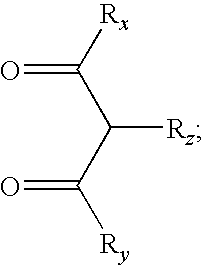
- separating unreacted
-

- and the product
-

- by column chromatography using a stationary phase consisting of alumina; wherein Rx and Ry are each independently selected from the group consisting of hydrogen, alkyl, heteroalkyl, aryl, or heteroaryl groups; wherein Rz is selected from the group consisting of alkyl, heteroalkyl, aryl, or heteroaryl groups; and wherein X═Cl, Br, I, OTf, OTs or OH.
- An organometallic compound is also provided, the organometallic compound containing a structure selected from the group consisting of:
-

-
FIG. 1 shows an organic light emitting device. -
FIG. 2 shows an inverted organic light emitting device that does not have a separate electron transport layer. -
FIG. 3 shows an example of an iridium compound. - Generally, an OLED comprises at least one organic layer disposed between and electrically connected to an anode and a cathode. When a current is applied, the anode injects holes and the cathode injects electrons into the organic layer(s). The injected holes and electrons each migrate toward the oppositely charged electrode. When an electron and hole localize on the same molecule, an “exciton,” which is a localized electron-hole pair having an excited energy state, is formed. Light is emitted when the exciton relaxes via a photoemissive mechanism. In some cases, the exciton may be localized on an excimer or an exciplex. Non-radiative mechanisms, such as thermal relaxation, may also occur, but are generally considered undesirable.
- The initial OLEDs used emissive molecules that emitted light from their singlet states (“fluorescence”) as disclosed, for example, in U.S. Pat. No. 4,769,292, which is incorporated by reference in its entirety. Fluorescent emission generally occurs in a time frame of less than 10 nanoseconds.
- More recently, OLEDs having emissive materials that emit light from triplet states (“phosphorescence”) have been demonstrated. Baldo et al., “Highly Efficient Phosphorescent Emission from Organic Electroluminescent Devices,” Nature, vol. 395, 151-154, 1998; (“Baldo-I”) and Baldo et al., “Very high-efficiency green organic light-emitting devices based on electrophosphorescence,” Appl. Phys. Lett., vol. 75, No. 3, 4-6 (1999) (“Baldo-II”), which are incorporated by reference in their entireties. Phosphorescence is described in more detail in U.S. Pat. No. 7,279,704 at cols. 5-6, which are incorporated by reference.
-
FIG. 1 shows an organiclight emitting device 100. The figures are not necessarily drawn to scale.Device 100 may include asubstrate 110, ananode 115, ahole injection layer 120, ahole transport layer 125, anelectron blocking layer 130, anemissive layer 135, ahole blocking layer 140, anelectron transport layer 145, anelectron injection layer 150, aprotective layer 155, and acathode 160.Cathode 160 is a compound cathode having a firstconductive layer 162 and a secondconductive layer 164.Device 100 may be fabricated by depositing the layers described, in order. The properties and functions of these various layers, as well as example materials, are described in more detail in U.S. Pat. No. 7,279,704 at cols. 6-10, which are incorporated by reference. - More examples for each of these layers are available. For example, a flexible and transparent substrate-anode combination is disclosed in U.S. Pat. No. 5,844,363, which is incorporated by reference in its entirety. An example of a p-doped hole transport layer is m-MTDATA doped with F.sub.4-TCNQ at a molar ratio of 50:1, as disclosed in U.S. Patent Application Publication No. 2003/0230980, which is incorporated by reference in its entirety. Examples of emissive and host materials are disclosed in U.S. Pat. No. 6,303,238 to Thompson et al., which is incorporated by reference in its entirety. An example of an n-doped electron transport layer is BPhen doped with Li at a molar ratio of 1:1, as disclosed in U.S. Patent Application Publication No. 2003/0230980, which is incorporated by reference in its entirety. U.S. Pat. Nos. 5,703,436 and 5,707,745, which are incorporated by reference in their entireties, disclose examples of cathodes including compound cathodes having a thin layer of metal such as Mg:Ag with an overlying transparent, electrically-conductive, sputter-deposited ITO layer. The theory and use of blocking layers is described in more detail in U.S. Pat. No. 6,097,147 and U.S. Patent Application Publication No. 2003/0230980, which are incorporated by reference in their entireties. Examples of injection layers are provided in U.S. Patent Application Publication No. 2004/0174116, which is incorporated by reference in its entirety. A description of protective layers may be found in U.S. Patent Application Publication No. 2004/0174116, which is incorporated by reference in its entirety.
-
FIG. 2 shows aninverted OLED 200. The device includes asubstrate 210, acathode 215, anemissive layer 220, ahole transport layer 225, and ananode 230.Device 200 may be fabricated by depositing the layers described, in order. Because the most common OLED configuration has a cathode disposed over the anode, anddevice 200 hascathode 215 disposed underanode 230,device 200 may be referred to as an “inverted” OLED. Materials similar to those described with respect todevice 100 may be used in the corresponding layers ofdevice 200.FIG. 2 provides one example of how some layers may be omitted from the structure ofdevice 100. - The simple layered structure illustrated in
FIGS. 1 and 2 is provided by way of non-limiting example, and it is understood that embodiments of the invention may be used in connection with a wide variety of other structures. The specific materials and structures described are exemplary in nature, and other materials and structures may be used. Functional OLEDs may be achieved by combining the various layers described in different ways, or layers may be omitted entirely, based on design, performance, and cost factors. Other layers not specifically described may also be included. Materials other than those specifically described may be used. Although many of the examples provided herein describe various layers as comprising a single material, it is understood that combinations of materials, such as a mixture of host and dopant, or more generally a mixture, may be used. Also, the layers may have various sublayers. The names given to the various layers herein are not intended to be strictly limiting. For example, indevice 200,hole transport layer 225 transports holes and injects holes intoemissive layer 220, and may be described as a hole transport layer or a hole injection layer. In one embodiment, an OLED may be described as having an “organic layer” disposed between a cathode and an anode. This organic layer may comprise a single layer, or may further comprise multiple layers of different organic materials as described, for example, with respect toFIGS. 1 and 2 . - Structures and materials not specifically described may also be used, such as OLEDs comprised of polymeric materials (PLEDs) such as disclosed in U.S. Pat. No. 5,247,190 to Friend et al., which is incorporated by reference in its entirety. By way of further example, OLEDs having a single organic layer may be used. OLEDs may be stacked, for example as described in U.S. Pat. No. 5,707,745 to Forrest et al, which is incorporated by reference in its entirety. The OLED structure may deviate from the simple layered structure illustrated in
FIGS. 1 and 2 . For example, the substrate may include an angled reflective surface to improve out-coupling, such as a mesa structure as described in U.S. Pat. No. 6,091,195 to Forrest et al., and/or a pit structure as described in U.S. Pat. No. 5,834,893 to Bulovic et al., which are incorporated by reference in their entireties. - Unless otherwise specified, any of the layers of the various embodiments may be deposited by any suitable method. For the organic layers, preferred methods include thermal evaporation, ink-jet, such as described in U.S. Pat. Nos. 6,013,982 and 6,087,196, which are incorporated by reference in their entireties, organic vapor phase deposition (OVPD), such as described in U.S. Pat. No. 6,337,102 to Forrest et al., which is incorporated by reference in its entirety, and deposition by organic vapor jet printing (OVJP), such as described in U.S. patent application Ser. No. 10/233,470, which is incorporated by reference in its entirety. Other suitable deposition methods include spin coating and other solution based processes. Solution based processes are preferably carried out in nitrogen or an inert atmosphere. For the other layers, preferred methods include thermal evaporation. Preferred patterning methods include deposition through a mask, cold welding such as described in U.S. Pat. Nos. 6,294,398 and 6,468,819, which are incorporated by reference in their entireties, and patterning associated with some of the deposition methods such as ink-jet and OVJD. Other methods may also be used. The materials to be deposited may be modified to make them compatible with a particular deposition method. For example, substituents such as alkyl and aryl groups, branched or unbranched, and preferably containing at least 3 carbons, may be used in small molecules to enhance their ability to undergo solution processing. Substituents having 20 carbons or more may be used, and 3-20 carbons is a preferred range. Materials with asymmetric structures may have better solution processibility than those having symmetric structures, because asymmetric materials may have a lower tendency to recrystallize. Dendrimer substituents may be used to enhance the ability of small molecules to undergo solution processing.
- Devices fabricated in accordance with embodiments of the invention may be incorporated into a wide variety of consumer products, including flat panel displays, computer monitors, televisions, billboards, lights for interior or exterior illumination and/or signaling, heads up displays, fully transparent displays, flexible displays, laser printers, telephones, cell phones, personal digital assistants (PDAs), laptop computers, digital cameras, camcorders, viewfinders, micro-displays, vehicles, a large area wall, theater or stadium screen, or a sign. Various control mechanisms may be used to control devices fabricated in accordance with the present invention, including passive matrix and active matrix. Many of the devices are intended for use in a temperature range comfortable to humans, such as 18 degrees C. to 30 degrees C., and more preferably at room temperature (20-25 degrees C.).
- The materials and structures described herein may have applications in devices other than OLEDs. For example, other optoelectronic devices such as organic solar cells and organic photodetectors may employ the materials and structures. More generally, organic devices, such as organic transistors, may employ the materials and structures.
- The terms halo, halogen, alkyl, cycloalkyl, alkenyl, alkynyl, arylkyl, heterocyclic group, aryl, aromatic group, and heteroaryl are known to the art, and are defined in U.S. Pat. No. 7,279,704 at cols. 31-32, which are incorporated herein by reference.
- Numerous Ir(2-phenylquinoline) and Ir(1-phenylisoquinoline) type phosphorescent materials have been synthesized, and OLEDs incorporating them as the dopant emitters have been fabricated. The devices may exhibit advantageously exhibit high current efficiency, high stability, narrow emission, improved processibility (e.g., high solubility and low sublimation temperature), and/or high luminous efficiency: quantum efficiency ratio (LE:EQE).
- Using Ir(3-Meppy)3 as a base structure, different alkyl substitution patterns on both the emitting ligand and the ancillary ligand were studied to establish a structure-property relationship with respect to material processibility (evaporation temperature, evaporation stability, solubility, etc) and device characteristics of Ir(2-phenylquinoline) and Ir(1-phenylisoquinoline) type phosphorescent materials and their PHOLEDs. Alkyl substitutions are particularly important because they offer a wide range of tunability in terms of evaporation temperature, solubility, energy levels, device efficiency and narrowness of the emission spectrum. Moreover, they are stable functional groups chemically and in device operation when applied appropriately.
- Compounds are provided, the compounds having the formula (also illustrated in
FIG. 3 ): -

- wherein M is a metal of atomic weight higher than 40; wherein A and B are each independently a 5 or 6-membered aromatic or heteroaromatic ring, and A-B represents a bonded pair of aromatic or heteroaromatic rings coordinated to the metal via a nitrogen atom on ring A and an sp2 hybridized carbon atom on ring B; wherein Ra, Rb, Rx, Ry, Rz are each independently selected from the group consisting of no substitution, alkyl, heteroalkyl, aryl, or heteroaryl groups; wherein each of Ra and Rb represent one or more substituents and can join to form fused rings; wherein at least one of Rx and Ry contains a branched alkyl moiety with branching at a position further than the α position to the carbonyl group; wherein m is the oxidation state of the metal; and wherein n is an integer less than m and at least 1.
- The compound may have the formula:
-

- The bonded pair of aromatic or heteroaromatic rings present in the compound, represented by A-B, is selected from the group consisting of:
-

- wherein X is N—R, O or S; and wherein R is selected from the group consisting of hydrogen, alkyl, heteroalkyl, aryl, and heteroaryl groups.
- Additionally, the compound may have the formula:
-

- In one example, Rx and Ry are an isobutyl group. In another example, Rz is hydrogen. Exemplary compounds include compound that are selected from the group consisting of:
-

- Additionally, compounds are provided wherein Rz is methyl. A specific example of such a compound includes
-

- The compounds described herein provide high device efficiency and stability, and a very narrow spectrum among other desirable properties. It is thought that a branched substituents at least at one of Rx and Ry, in combination with the methyl substituents on the phenyl ring (ring B) of the compound may provide for the very narrow emission spectrum and other remarkably good properties of the compound.
- Additionally, specific compounds are provided wherein the compound is selected from the group consisting of:
-


- An organic light emitting device is also provided. The device comprises an anode, a cathode, and an organic layer that is disposed between the anode and the cathode. The organic layer further comprising a compound having the formula:
-

- wherein M is a metal of atomic weight higher than 40; wherein A and B are each independently a 5 or 6-membered aromatic or heteroaromatic ring, and A-B represents a bonded pair of aromatic or heteroaromatic rings coordinated to the metal via a nitrogen atom on ring A and an sp2 hybridized carbon atom on ring B; wherein Ra, Rb, Rx, Ry, Rz are each independently selected from the group consisting of no substitution, alkyl, heteroalkyl, aryl, or heteroaryl groups; wherein each of Ra and Rb represent one or more substituents; wherein at least one of Rx and Ry contains a branched alkyl moiety with branching at a position further than the α position to the carbonyl group; wherein m is the oxidation state of the metal; and wherein n is an integer less than m and at least 1.
- The device can contain the compound
-

- The device can contain a compound wherein A-B of the compound is selected from the group consisting of:
-

- wherein X is N—R, O or S; and wherein R is selected from the group consisting of no substitution, alkyl, heteroalkyl, aryl, and heteroaryl groups.
- Additionally, the device can contain a compound having the formula:
-

- In one example, the device can contain a compound wherein Rx and Ry are an isobutyl group. In another example, the device can contain a compound wherein Rz is hydrogen. In yet another example, the device can contain a compound selected from the group consisting of:
-

- Additionally, the device can contain a compound wherein Rz is methyl. Moreover, in one example, the device can contain the compound
-

- The organic layer of the device is an emissive layer comprising the compound and a host. In one example, the compound is the emissive material. In another example, the host is a metal coordination complex. The host material can be BAlq. In another example, the compound of the device is the emissive material and the host is a metal coordination complex. The host material can be BAlq.
- Additionally, an organic light emitting device is provided. The device comprises an anode, a cathode, and an organic layer disposed between the anode and the cathode, the organic layer comprising a compound selected from the group consisting of:
-


- Additionally, the organic later of the device can be an emissive layer comprising the compound and a host. The inventive compound can be the emissive material and the host can be a metal coordination complex. For example, the host can be BAlq.
- A consumer product is also provided. The consumer product comprising a device, the device further comprising an anode, a cathode, and an organic layer disposed between the anode and the cathode. The organic layer further comprising a compound having the formula:
-

- wherein M is a metal of atomic weight higher than 40; wherein A and B are each independently a 5 or 6-membered aromatic or heteroaromatic ring, and A-B represents a bonded pair of aromatic or heteroaromatic rings coordinated to the metal via a nitrogen atom on ring A and an sp2 hybridized carbon atom on ring B; wherein Ra, Rb, Rx, Ry, Rz are each independently selected from the group consisting of no substitution, alkyl, heteroalkyl, aryl, or heteroaryl groups; wherein each of Ra and Rb represent one or more substituents; wherein at least one of Rx and Ry contains a branched alkyl moiety with branching at a position further than the α position to the carbonyl group; wherein m is the oxidation state of the metal; and wherein n is at least 1.
- Additionally, a consumer device is provided wherein the consumer product comprises a device, the device further comprising an anode, a cathode, and an organic layer disposed between the anode and the cathode. The organic layer further comprising a compound selected from the group consisting of:
-


- Additionally, a method is provided comprising reacting
-

- with Rz-X to form the free base
-

- separating unreacted
-

- and the product
-

- by column chromatography using a stationary phase consisting of alumina; wherein Rx and Ry are each independently selected from the group consisting of hydrogen, alkyl, heteroalkyl, aryl, or heteroaryl groups; wherein Rz is selected from the group consisting of alkyl, heteroalkyl, aryl, or heteroaryl groups; and wherein X═Cl, Br, I, OTf, OTs or OH.
- The method can further comprise reacting
-

- with a metal M and one or more ligands to form a compound having the formula:
-

- wherein M is a metal of atomic weight higher than 40; wherein A and B are each independently a 5 or 6-membered aromatic or heteroaromatic ring, and A-B represents a bonded pair of aromatic or heteroaromatic rings coordinated to the metal via a nitrogen atom on ring A and an sp2 hybridized carbon atom on ring B; wherein RA and RB each represent no substitution or one or more substituents; wherein each substituent of RA and RB is independently selected from the group consisting of alkyl, heteroalkyl, aryl, or heteroaryl groups; wherein m is the oxidation state of the metal; and wherein n is an integer less than m and at least 1.
- Additionally, the method can further comprise wherein Rz is a methyl group; and wherein
-

- Isotopic analogues of the compounds provided herein where hydrogen has been replaced by deuterium are also included.
- Additionally, an organometallic compound is provided. The organometallic compound contains a structure selected from the group consisting of
-

- wherein M is a metal with an atomic weight greater than 40.
- The organometallic compound provided can have M as Ir.
- The organometallic compound provided can be a phosphorescent material.
- The materials described herein as useful for a particular layer in an organic light emitting device may be used in combination with a wide variety of other materials present in the device. For example, emissive dopants disclosed herein may be used in conjunction with a wide variety of hosts, transport layers, blocking layers, injection layers, electrodes and other layers that may be present. The materials described or referred to below are non-limiting examples of materials that may be useful in combination with the compounds disclosed herein, and one of skill in the art can readily consult the literature to identify other materials that may be useful in combination.
- In addition to and/or in combination with the materials disclosed herein, many hole injection materials, hole transporting materials, host materials, dopant materials, exiton/hole blocking layer materials, electron transporting and electron injecting materials may be used in an OLED. Non-limiting examples of the materials that may be used in an OLED in combination with materials disclosed herein are listed in Table 1 below. Table 1 lists non-limiting classes of materials, non-limiting examples of compounds for each class, and references that disclose the materials.
-
TABLE 1 MATERIAL EXAMPLES OF MATERIAL PUBLICATIONS Hole injection materials Phthalocyanine and porphryin compounds 
Appl. Phys. Lett. 69, 2160 (1996) Starburst triarylamines 
J. Lumin. 72-74, 985 (1997) CFx Fluorohydrocarbon CHxFyn Appl. Phys. Lett. 78, polymer 673 (2001) Conducting polymers (e.g., PEDOT:PSS, polyaniline, polypthiophene) 
Synth. Met. 87, 171 (1997) Arylamines complexed with metal oxides such as molybdenum and tungsten oxides 
SID Symposium Digest, 37, 923 (2006) Hole transporting materials Triarylamines (e.g., TPD, α-NPD) 
Appl. Phys. Lett. 51, 913 (1987) 
US5061569 
EP650955 
J. Mater. Chem. 3, 319 (1993) 
Appl. Phys. Lett. 90, 183503 (2007) 
Appl. Phys. Lett. 90, 183503 (2007) Triaylamine on spirofluorene core 
Synth. Met. 91, 209 (1997) Arylamine carbazole compounds 
Adv. Mater. 6, 677 (1994) Indolocarbazoles 
Synth. Met. 111, 421 (2000) Isoindole compounds 
Chem. Mater. 15, 3148 (2003) Phosphorescent OLED host materials Red hosts Arylcarbazoles 
Appl. Phys. Lett. 78, 1622 (2001) Metal 8-hydroxyquinolates (e.g., Alq3, BAlq) 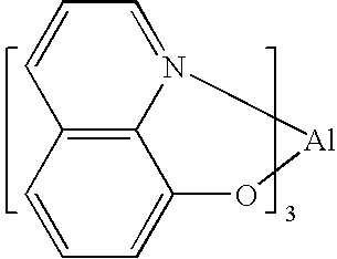
Nature 395, 151 (1998) 
US20060202194 
WO2005014551 Metal phenoxybenzothiazole compounds 
Appl. Phys. Lett. 90, 123509 (2007) Conjugated oligomers and polymers (e.g., polyfluorene) 
Org. Electron. 1, 15 (2000) Green hosts Arylcarbazoles 
Appl. Phys. Lett. 78, 1622 (2001) 
US2003175553 
WO2001039234 Aryltriphenylene compounds 
US20060280965 
US20060280965 Polymers (e.g., PVK) 
Appl. Phys. Lett. 77, 2280 (2000) Spirofluorene compounds 
WO2004093207 Metal phenoxybenzooxazole compounds 
WO05089025 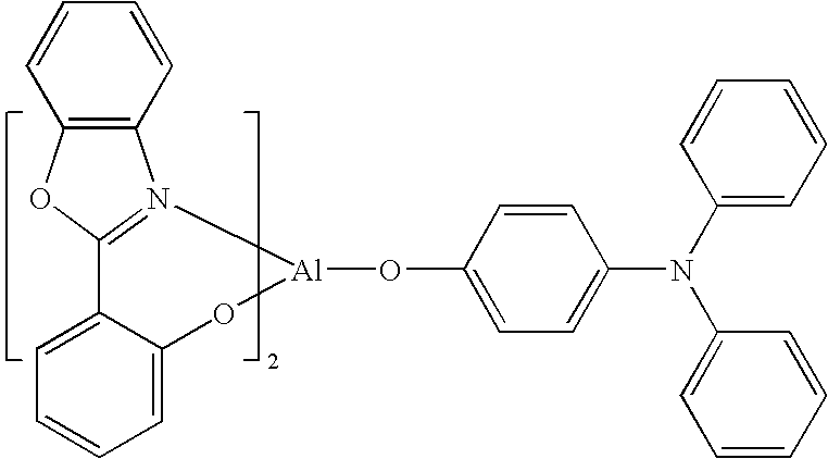
WO06132173 
JP200511610 Spirofluorene-carbazole compounds 
JP2007254297 
JP2007254297 Indolocabazoles 
WO07063796 
WO07063754 5-member ring electron deficient heterocycles (e.g., triazole, oxadiazole) 
J. Appl. Phys. 90, 5048 (2001) 
WO04107822 Metal phenoxypyridine compounds 
WO05030900 Blue hosts Arylcarbazoles 
Appl. Phys. Lett, 82, 2422 (2003) 
US20070190359 Dibenzothiophene- carbazole compounds 
WO2006114966 Phosphorescent dopants Red dopants Heavy metal porphyrins (e.g., PtOEP) 
Nature 395, 151 (1998) Iridium(III) organometallic complexes 
Appl. Phys. Lett. 78, 1622 (2001) 
US06835469 
US06835469 
US20060202194 
US20060202194 
US07087321 
US07087321 
Adv. Mater. 19, 739 (2007) Platinum(II) organometallic complexes 
WO2003040257 Osminum(III) complexes 
Chem. Mater. 17, 3532 (2005) Ruthenium(II) complexes 
Adv. Mater. 17, 1059 (2005) Green dopants Iridium(III) organometallic complexes 
Inorg. Chem. 40, 1704 (2001) 
US2002034656 
US06687266 
Chem. Mater. 16, 2480 (2004) 
US2007190359 
US 2006008670 JP2007123392 
Adv. Mater. 16, 2003 (2004) 
Angew. Chem. Int. Ed. 2006, 45, 7800 Pt(II) organometallic complexes 
Appl. Phys. Lett. 86, 153505 (2005) 
Appl. Phys. Lett. 86, 153505 (2005) 
Chem. Lett. 34, 592 (2005) Gold complexes 
Chem. Commun. 2906 (2005) Rhenium(III) complexes 
Inorg. Chem. 42, 1248 (2003) Blue dopants Iridium(III) organometallic complexes 
WO2002002714 
WO2006009024 
US2006251923 
WO2006056418, US2005260441 
US2007190359 
US2002134984 
Angew. Chem. Int. Ed. 47, 1 (2008) 
Chem. Mater. 18, 5119 (2006) 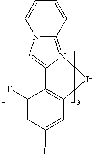
Inorg. Chem. 46, 4308 (2007) 
WO05123873 
WO05123873 
WO07004380 
WO06082742 Osmium(II) complexes 
US2005260449 
Organometallics 23, 3745 (2004) Gold complexes 
Appl. Phys. Lett. 74, 1361 (1999) Platinum(II) complexes 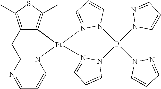
WO06098120, WO06103874 Exciton/hole blocking layer materials Bathocuprine compounds (e.g., BCP, BPhen) 
Appl. Phys. Lett. 75, 4 (1999) 
Appl. Phys. Lett. 79, 449 (2001) Metal 8-hydroxyquinolates (e.g., BAlq) 
Appl. Phys. Lett. 81, 162 (2002) 5-member ring electron deficient heterocycles such as triazole, oxadiazole, imidazole, benzoimidazole 
Appl. Phys. Lett. 81, 162 (2002) Triphenylene compounds 
US20050025993 Fluorinated aromatic compounds 
Appl. Phys. Lett. 79, 156 (2001) Electron transporting materials Anthracene- benzoimidazole compounds 
WO03060956 Anthracene-benzothiazole compounds 
Appl. Phys. Lett. 89, 063504 (2006) Metal 8-hydroxyquinolates (e.g., Alq3) 
Appl. Phys. Lett. 51, 913 (1987) Metal hydroxybenoquinolates 
Chem. Lett. 5, 905 (1993) Bathocuprine compounds such as BCP, BPhen, etc 
Appl. Phys. Lett. 91, 263503 (2007) 
Appl. Phys. Lett. 79, 449 (2001) 5-member ring electron deficient heterocycles (e.g., triazole, oxadiazole, imidazole, benzoimidazole) 
Appl. Phys. Lett. 74, 865 (1999) 
Appl. Phys. Lett. 55, 1489 (1989) 
Jpn. J. Apply. Phys. 32, L917 (1993) Silole compounds 
Org. Electron. 4, 113 (2003) Arylborane compounds 
J. Am. Chem. Soc. 120, 9714 (1998) Fluorinated aromatic compounds 
J. Am. Chem. Soc. 122, 1832 (2000) -

- 2-chloroquinoline (9.0 g, 54.4 mmol), 3,5-dimethylphenylboronic acid (9.2 g, 59.8 mmol), Pd(PPh3)4 (1.8 g, 1.5 mmol), K2CO3(22.4 g, 163 mmol), 1,2-dimethoxyethane (150 mL) and water (150 mL) were charged in a 500 mL round bottom flask. The reaction mixture was heated to reflux under nitrogen for 18 h. The reaction mixture was then cooled to ambient and the organic phase was separated from the aqueous phase. The aqueous phase was washed with ethyl acetate and all the organic components were combined and dried over anhydrous magnesium sulphate. The solvent was then removed under vacuum and the product was purified using silica gel chromatography (10% ethyl acetate in hexane as eluent). The material obtained was further purified by vacuum distillation to yield 12.2 g (95% yield) of product as a colorless oil.
-

- The ligand from step 1 (46 g, 197.4 mmol), 2-ethoxyethanol (536 mL) and water (178 mL) were charged in a 1 L three-neck round bottom flask. Nitrogen gas was bubbled through the reaction mixture 45 min. IrCl3.H2O (32.0 g 86.2 mmol) was then added and the reaction mixture was heated to reflux under nitrogen for 17 hours. The reaction mixture was cooled to ambient and filtered. The dark gray residue was washed with methanol (4×150 mL) followed by hexanes (3×300 mL). 36.5 gram of the dichlorobridged Iridium dimer was obtained after drying in vacuum oven.
-

- Dichlorobridged Iridium dimer from step 2 (3.0 g, 2.2 mmol), 10 mol eq 3-methyl-2,4-pentanedione (2.5 g,), 20 mol eq of Na2CO3 (6.3 g) and 25 mL of 2-ethoxyethanol were placed in a 250 mL round bottom flask. The reaction mixture was stirred at ambient for 24 hours. 2 g of celite and 200 mL of dichloromethane was added to the reaction mixture to dissolve the product. The mixture was then filtered through a bed of celite. The filtrate was then passed through a through a silica/alumina plug and washed with dichloromethane. The clarified solution was then filtered through GF/F filter paper the filtrate was heated to remove most of the dichloromethane. 20 mL of isopropanol was then added and the slurry was cooled to ambient and the product was filtered and washed with isopropanol and dried to give 3.2 g of crude product (97% yield). This product was then recrystallised twice using dichloromethane and isopropanol and then sublimed.
-

- 2-chloro-3-methyl-quinoline (4.5 g, 25.0 mmol), dimethylphenylboronic acid (4.6 g, 30 mmol), triphenylphosphine (1.60 g, 6.11 mmol), and potassium carbonate (12.67 g, 91.69 mmol) were charged in a 250 mL round bottom flask. 25 mL water and 25 mL of dimethoxyethane was added to the flask. Nitrogen was bubbled through the reaction mixture for 30 min. Palladium acetate (0.34 g, 1.53 mmol) was then added to the reaction mixture was then refluxed overnight under an atmosphere of nitrogen. The product was extracted with ethyl acetate, washed with water, and dried over anhydrous magnesium sulfate. The product was purified using silica gel chromatography (5-15% ethyl acetate in hexane as eluent) to give a light yellow oil (85% yield). Further purification was done via vacuum distillation
-

- Ligand from step 1 (16 g, 65 mmol), iridium chloride (5.0 g, 14 mmol), 2-ethoxyethanol (75 mL) and water (12.5 mL) was charged in a 250 mL round bottom flask. The reactor contents were heated to 102° C. under an atmosphere of nitrogen for 16-19 h. The dichloro iridium bridged dimer was not isolated.
-

- The reactor contents from step 2 were cooled to ambient. 2,4-pentanedione (14.0
g 140 mmol) and sodium carbonate (30.0 g, 280 mmol) were added to the reactor. The reaction mixture was stirred at ambient for 24 h. 5 g of celite and 500 mL of dichloromethane was added to the reaction mixture to dissolve the product. The mixture was then filtered through a bed of celite. The filtrate was then passed through a through a silica/alumina plug and washed with dichloromethane. The clarified solution was then filtered through GF/F filter paper the filtrate was heated to remove most of the dichloromethane. 20 mL of isopropanol was then added and the slurry was cooled to ambient and the product was filtered and washed with isopropanol and dried to give 6.3 g of crude product (57% yield). This product was then recrystallised twice using dichloromethane and isopropanol and then sublimed. -

- 2-chloroquinoline (9.0 g, 54.4 mmol), 3,5-dimethyiphenylboronic acid (9.2 g, 59.8 mmol), Pd(PPh3)4 (1.8 g, 1.5 mmol), K2CO3 (22.4 g, 163 mmol), 1,2-dimethoxyethane (150 mL) and water (150 mL) were charged in a 500 mL round bottom flask. The reaction mixture was heated to reflux under nitrogen for 18 h. The reaction mixture was then cooled to ambient and the organic phase was separated from the aqueous phase. The aqueous phase was washed with ethyl acetate and all the organic components were combined and dried over anhydrous magnesium sulphate. The solvent was then removed under vacuum and the product was purified using silica gel chromatography (10% ethyl acetate in hexane as eluent). The material obtained was further purified by vacuum distillation to yield 12.2 g (95% yield) of product as a colorless oil.
-

- The ligand from step 1 (46 g, 197.4 mmol), 2-ethoxyethanol (536 mL) and water (178 mL) were charged in a 1 L three-neck round bottom flask. Nitrogen gas was bubbled through the reaction mixture 45 min. IrCl3.H2O (32.0 g 86.2 mmol) was then added and the reaction mixture was heated to reflux under nitrogen for 17 hours. The reaction mixture was cooled to ambient and filtered. The dark gray residue was washed with methanol (4×150 mL) followed by hexanes (3×300 mL). 36.5 gram of the dichlorobridged Iridium dimer was obtained after drying in vacuum oven.
-

- N,N dimethylformamide (DMF) (1 L) and potassium tert-butoxide (135.0 g 1.2 mol) were heated to 50 C under nitrogen. Methyl 3-methylbutanoate (86.0 g, 0.75 mol) was added dropwise from a dropping funnel followed by a solution of 4-methylpentane-2-one (50 g, 1 mol) in 100 mL DMF. The progress of the reaction was monitored by GC. When the reaction was completed, the mixture was cooled to ambient and slowly neutralized with 20% H2SO4 solution. Water (300 mL) was added and two layers formed. The layer containing the 2,8-dimethylnonane-4,6-dione was purified using vacuum distillation to give 40 g of a pink oil (43% yield)
-

- Dichlorobridged Iridium dimer from step 2 (3.0 g, 2.2 mmol), 10 mol eq 2,8-dimethylnonane-4,6-dione (4.1 g,), 20 mol eq of Na2CO3 (6.3 g) and 25 mL of 2-ethoxyethanol were placed in a 250 mL round bottom flask. The reaction mixture was stirred at ambient for 24 hours. 2 g of celite and 200 mL of dichloromethane was added to the reaction mixture to dissolve the product. The mixture was then filtered through a bed of celite. The filtrate was then passed through a through a silica/alumina plug and washed with dichloromethane. The clarified solution was then filtered through GF/F filter paper the filtrate was heated to remove most of the dichloromethane. 20 mL of isopropanol was then added and the slurry was cooled to ambient and the product was filtered and washed with isopropanol and dried to give 2.9 g of crude product (79% yield). This product was then recrystallised twice using dichloromethane and isopropanol and then sublimed.
-

- Dichloroiodobenzene (37.0 g 136 mmol), Pd2(dba)3 (1.5 g, 1.6 mmol), Lithium chloride (29.0 g, 682 mmol) was dissolved in 100 mL of DMF in a 500 mL round bottom flask. 64.0 mL of acetic anhydride and 47.0 mL of N-Ethyldiispropylamine was then added to the reaction mixture. The reaction was heated to 100° C. for 8 hours. Water was added to the reaction mixture and the product was extracted with ethylacetate and chromatographed using a silica gel column with ethyl acetate and hexanes as the eluent. 8 g of product was obtained.
-

- 2-aminobenzyl alcohol (6.0 g, 48 mmol), 3,5-dichloroacetophenone (12.0 g, 63.5 mmol), RuCl2(PPh3)3 (0.5 g 10 mol %), and KOH (2.4 g, 42.0 mmol) was refluxed in 100 ml of toluene for 10 hours. Water was collected from the reaction using a Dean-Stark trap. The reaction mixture was allowed to cool to room temperature and filtered through a silica gel plug. The product was further purified with a silica gel column using 2% ethyl acetate in hexanes as the eluent. 4.0 g product was obtained after column (30% yield). The product was further recrystallized from isopropanol. 3.5 g of desired product was obtained.
-

- 2-(3,5-dichlorophenyl)quinoline (4.0 g, 14.6 mmol), isobutylboronic acid (6.0 g, 58.4 mol), Pd2(dba)3 (0.13 g, 1 mol %), dicyclohexylphosphino-2′,6′-dimethoxybiphenyl (0.24, 4 mol %), potassium phosphate monohydrate (10 g, 13.8 mmolmol) was mixed in 100 mL of toluene in a 250 mL round bottom flask. Nitrogen was bubbled through the mixture for 20 minutes and the mixture refluxed in a nitrogen atmosphere overnight. The reaction mixture was allowed to cool and the solvent removed under vacuum. The crude product was chromatographed using a silica gel column with 2% ethyl acetate in hexanes as the eluent. The solvent was then removed under vacuo to give 3.5 g of product.
-

- Ligand from step 3 (20 g, 65 mmol), iridium chloride (5.0 g, 14 mmol), 2-ethoxyethanol (75 mL) and water (12.5 mL) was charged in a 250 mL round bottom flask. The reactor contents were heated to 102° C. under an atmosphere of nitrogen for 16-19 h. The dichloro iridium bridged dimer was not isolated.
-

- The reactor contents from step 4 were cooled to ambient. 2,4-pentanedione (14.0
g 140 mmol) and sodium carbonate (30.0 g, 280 mmol) were added to the reactor. The reaction mixture was stirred at ambient for 24 h. 5 g of celite and 500 mL of dichloromethane was added to the reaction mixture to dissolve the product. The mixture was then filtered through a bed of celite. The filtrate was then passed through a through a silica/alumina plug and washed with dichloromethane. The clarified solution was then filtered through GF/F filter paper the filtrate was heated to remove most of the dichloromethane. 20 mL of isopropanol was then added and the slurry was cooled to ambient and the product was filtered and washed with isopropanol and dried to give 7.1 g of crude product (55% yield). This product was then recrystallised twice using dichloromethane and isopropanol and then sublimed. -

- 2-chloroquinoline (9.0 g, 54.4 mmol), 3,5-dimethylphenylboronic acid (9.2 g, 59.8 mmol), Pd(PPh3)4 (1.8 g, 1.5 mmol), K2CO3 (22.4 g, 163 mmol), 1,2-dimethoxyethane (150 mL) and water (150 mL) were charged in a 500 mL round bottom flask. The reaction mixture was heated to reflux under nitrogen for 18 h. The reaction mixture was then cooled to ambient and the organic phase was separated from the aqueous phase. The aqueous phase was washed with ethyl acetate and all the organic components were combined and dried over anhydrous magnesium sulphate. The solvent was then removed under vacuum and the product was purified using silica gel chromatography (10% ethyl acetate in hexane as eluent). The material obtained was further purified by vacuum distillation to yield 12.2 g (95% yield) of product as a colorless oil.
-

- The ligand from step 1 (46 g, 197.4 mmol), 2-ethoxyethanol (536 mL) and water (178 mL) were charged in a 1 L three-neck round bottom flask. Nitrogen gas was bubbled through the reaction mixture 45 min. IrCl3.H2O (32.0 g 86.2 mmol) was then added and the reaction mixture was heated to reflux under nitrogen for 17 hours. The reaction mixture was cooled to ambient and filtered. The dark gray residue was washed with methanol (4×150 mL) followed by hexanes (3×300 mL). 36.5 gram of the dichlorobridged Iridium dimer was obtained after drying in vacuum oven.
-

- 2,8-dimethylnonane-4,6-dione (10.0 g, 5.4 mmol), potassium tert butoxide (7.0 g, 6.5 mmol) and 150 mL of anhydrous THF was charged in a 3 neck 250 mL dry round bottom flask. The reaction mixture was stirred under an atmosphere of nitrogen at ambient for 1 h. Iodomethane (15 g, 105 mmol) was added to the reaction mixture via a needle and syringe. The reaction mixture was continued to stir at ambient for a further 4 h. The reaction was monitored by GC. The reaction was quenched with 100 mL of water and acidified using 1M hydrochloric acid. The product was extracted with ethyl acetate and chromatographed using silica gel chromatography (using 1-5% ethyl acetate in hexanes). HPLC revealed that the product (2,5,8-trimethylnonane-4,6-dione) contained a mixture of 2,8-dimethylnonane-4,6-dione (starting material). These to products were separated via chromatography using deactivated basic alumina with 1-5% ethyl acetate in hexanes as the mobile phase to give 3.6 g of product (33% yield).
-

- Dichlorobridged Iridium dimer from step 2 (1.0 g, 0.7 mmol), 10 mol eq 2,5,8-trimethylnonane-4,6-dione (1.4 g,), 20 mol eq of Na2CO3 (2.0 g) and 25 mL of 2-ethoxyethanol were placed in a 250 mL round bottom flask. The reaction mixture was stirred at ambient for 24 hours. 1 g of celite and 100 mL of dichloromethane was added to the reaction mixture to dissolve the product. The mixture was then filtered through a bed of celite. The filtrate was then passed through a through a silica/alumina plug and washed with dichloromethane. The clarified solution was then filtered through GF/F filter paper the filtrate was heated to remove most of the dichloromethane. 10 mL of isopropanol was then added and the slurry was cooled to ambient and the product was filtered and washed with isopropanol and dried to give 0.7 g of crude product (57% yield). This product was then recrystallised twice using dichloromethane and isopropanol and then sublimed.
-

- 4-chlorophenylethylamine hydrochloride (10.0 g, 64 mmol), pyridine (15.3 g, 193 mmol) and dichloromethane (50 mL) were added to a 3-neck round bottom flask. The solution was cooled in an ice bath and 3,5-dimethylbenzoyl chloride (10.8 g, 64 mmol) was added slowly. The solution was allowed to warm to room temperature and stirred for 12 hours. Dichloromethane was added and the organic phase was washed with water, followed by 5% HCl solution, then 5% NaOH solution and then dried over anhydrous MgSO4. The solvent was evaporated under vacuum resulting in 15 g of crude product (82% yield) which was used without further purification.
-

- N-(4-chlorophenylethyl)benzamide (15 g, 52 mmol), isobutylboronic acid (10.6 g, 104 mmol), Pd2(dba)3 (1 mol %), 2-dicyclohexylphosphino-2′,6′-dimethoxybiphenyl (4 mol %), potassium phosphate monohydrate (22.0 g 212 mmol) 200 ml of toluene was charged in a 250 mL round bottom flask. Nitrogen was bubbled through the reaction mixture for 20 minutes and heated to reflux for 18 h overnight. The reaction mixture was allowed to cool to ambient temperature and the crude product was purified by column chromatography using 2% ethyl acetate in hexanes as solvent. 15 g of desired product was obtained (93% yield).
-

- N-(4-p-isobutylphenylethyl)benzamide (15.0 g), phosphorous pentoxide (50 g) phosphorous oxychloride 50 mL and xylenes (160 mL) was refluxed for 3 h in a 1 L round bottom flask. After the reaction mixture was allowed to cool to room temperature, the solvent was decanted and ice was slowly added to the solid in the bottom of the flask. The water-residue mixture was made weakly alkaline with 50% NaOH and the product was extracted with toluene. The organic layer was washed with water and dried over anhydrous MgSO4. The solvent was evaporated to give 12.4 g of crude product (88% yield) which was used without further purification.
-

- 1-(3,5-dimethylphenyl)-7-isobutyl-3,4-dihydroisoquinoline (12.4 g, 42.5 mmol) and 2 g of 5% Pd/C (˜10% by weight) were added to a 500 mL round bottom flask with 100 mL of xylenes. The solution was refluxed for 24 hrs and the formation of the product was monitored by TLC. The solvent was removed under vacuum and the product was purified by silica gel column chromatography with 5% ethyl acetate in hexanes as the eluent. The product was then vacuum distilled to give (6.0 g, 21 mmol) of pure product.
-

- The ligand from step 4 (4.7 g, 14 mmol), 2-ethoxyethanol (25 mL) and water (5 mL) were charged in a 1 L three-neck round bottom flask. Nitrogen gas was bubbled through the reaction mixture for 45 min. IrCl3.H2O (1.2 g 3.6 mmol) was then added and the reaction mixture was heated to reflux under nitrogen for 17 hours. The reaction mixture was cooled to ambient and filtered. The dark red residue was washed with methanol (2×25 mL) followed by hexanes (2×25 mL). 2.5 g of the dichlorobridged Iridium dimer was obtained after drying in vacuum oven.
-

- Dichlorobridged Iridium dimer from step 5 (2.5 g, 1.5 mmol), 10 mol eq 2,8-dimethylnonane-4,6-dione (2.8 g,), 20 mol eq of Na2CO3 (4.3 g) and 25 mL of 2-ethoxyethanol were placed in a 250 mL round bottom flask. The reaction mixture was stirred at ambient for 24 hours. 2 g of celite and 200 mL of dichloromethane was added to the reaction mixture to dissolve the product. The mixture was then filtered through a bed of celite. The filtrate was then passed through a through a silica/alumina plug and washed with dichloromethane. The clarified solution was then filtered through GF/F filter paper the filtrate was heated to remove most of the dichloromethane. 20 mL of isopropanol was then added and the slurry was cooled to ambient and the product was filtered and washed with isopropanol and dried to give 2.5 g of crude product (86% yield). This product was then recrystallised twice using dichloromethane and isopropanol and then sublimed.
-

- 4-isopropylphenylethylamine hydrochloride (5.0 g, 25 mmol), pyridine (5.9 g, 75 mmol) and dichloromethane (25 mL) were added to a 3-neck round bottom flask. The solution was cooled in an ice bath and 3,5-dimethylbenzoyl chloride (4.2 g, 25 mmol) was added slowly. The solution was then allowed to warm to room temperature and stirred for 12 hours. Dichloromethane was added and the organic phase was washed with water, followed by 5% HCl solution, then 5% NaOH solution and then dried over anhydrous MgSO4. The solvent was evaporated under vacuum resulting in 7.5 g of crude product (82% yield) which was used without further purification.
-

- N-(4-p-isopropylphenylethyl)benzamide (7.5 g) in 80 mL xylenes was refluxed for 3 hrs together with 25 g phosphorous pentoxide and 25 mL phosphorous oxychloride. After cooling, the solvent was decanted and ice was slowly added to the solid in the bottom of the flask. The water-residue mixture was made weakly alkaline with 50% NaOH and the product was extracted with toluene. The organic layer was washed with water and dried over anhydrous MgSO4. The solvent was removed under vacuum to give 6.2 g of crude product which was used without further purification.
-

- 6.2 g of 7-isopropyl-1-phenyl-3,4-dihydroisoquinoline and 1 g of 5% Pd/C (˜10% by weight) were added to a round bottom flask with 100 mL of xylenes. The solution was refluxed for 24 hrs and the formation of the product was monitored by TLC. The xylenes solvent was removed and the product was purified by column chromatography with ethyl acetate/hexanes. The pure fractions were collected and the solvent was removed. The product was then distilled in a kugelrohr apparatus at 185° C. affording 1.8 g (0.0073 mol) of pure product. The overall yield of ligand formation was ˜15%.
-

- The ligand from step 3 (1.8 g, 7.3 mmol), 2-ethoxyethanol (25 mL) and water (5 mL) were charged in a 1 L three-neck round bottom flask. Nitrogen gas was bubbled through the reaction mixture 45 min. IrCl3.H2O (1.2 g 3.6 mmol) was then added and the reaction mixture was heated to reflux under nitrogen for 17 hours. The reaction mixture was cooled to ambient and filtered. The dark red residue was washed with methanol (2×25 mL) followed by hexanes (2×25 mL). 1.3 gram of the dichlorobridged Iridium dimer was obtained after drying in vacuum oven
-

- Dichlorobridged Iridium dimer from step 2 (1.3 g, 0.9 mmol), 10 mol eq 2,8-dimethylnonane-4,6-dione (1.6 g,), 20 mol eq of Na2CO3 (2.5 g) and 25 mL of 2-ethoxyethanol were placed in a 250 mL round bottom flask. The reaction mixture was stirred at ambient for 24 hours. 2 g of celite and 200 mL of dichloromethane was added to the reaction mixture to dissolve the product. The mixture was then filtered through a bed of celite. The filtrate was then passed through a through a silica/alumina plug and washed with dichloromethane. The clarified solution was then filtered through GF/F filter paper the filtrate was heated to remove most of the dichloromethane. 20 mL of isopropanol was then added and the slurry was cooled to ambient and the product was filtered and washed with isopropanol and dried to give 1.4 g of crude product (92% yield). This product was then recrystallised twice using dichloromethane and isopropanol and then sublimed.
-

- 2-amino-4-chlorobenzoic acid (42.8 g, 0.25 mol) was dissolved in 200 mL of anhydrous THF and cooled in an ice-water bath. To the solution was added lithium aluminum hydride chips (11.76 g, 0.31 mol). The resulting mixture was stirred at room temperature for 8 hours. 12 g of water was added, and then 12 g 15% NaOH. 36 g of water was then added. The slurry was stirred at room temperature for 30 min. The slurry was filtered. The solid was washed with ethyl acetate. The liquid was combined and the solvent was evaporated. The crude material was used for next step without purification.
-

- 2-amino-4-chlorophenyl)methanol (6.6 g, 0.04 mol) 1-(3,5-dimethylphenyl)ethanone (10.0 g 0.068 mol), RuCl2(PPh3)3 0.1 g) and 2.4 g of KOH was refluxed in 100 ml of toluene for 10 hours. Water was collected from the reaction using a Dean-Stark trap. After the reaction was cooled to room temperature, the mixture was filtered through a silica gel plug. The product was further purified with column chromatography using 2% ethyl acetate in hexanes as eluent. 9 g product was obtained after column. The product was further recrystallized from isopropanol. 5 g of desired product was obtained.
-

- 7-chloro-2-(3,5-dimethylphenyl)quinoline (3.75 g, 0.014 mol) isobutylboronic acid (2.8 g, 0.028 mol), Pd2(dba)3 (1 mol %), 2-dicyclohexylphosphino-2′,6′-dimethoxybiphenyl (4 mol %), potassium phosphate monohydrate (16.0 g) 100 mL of toluene was charged in a 250 mL round bottom flask. Nitrogen was bubbled through the reaction mixture for 20 minutes and heated to reflux for 18 h overnight. The reaction mixture was allowed to cool to ambient temperature and the crude product was purified by column chromatography using 2% ethyl acetate in hexanes as solvent. 3.6 g of desired product was obtained.
-

- The ligand from step 3 (4.6 g, 16 mmol), 2-ethoxyethanol (25 mL) and water (5 mL) were charged in a 1 L three-neck round bottom flask. Nitrogen gas was bubbled through the reaction mixture 45 min. IrCl3.H2O (1.2 g 3.6 mmol) was then added and the reaction mixture was heated to reflux under nitrogen for 17 hours. The reaction mixture was cooled to ambient and filtered. The dark red residue was washed with methanol (2×25 mL) followed by hexanes (2×25 mL). 1.3 gram of the dichlorobridged Iridium dimer was obtained after drying in vacuum oven
-

- Dichlorobridged Iridium dimer from step 2 (1.0 g, 0.6 mmol), 10 mol eq 3-methyl-2,4-pentanedione (0.8 g,), 20 mol eq of Na2CO3 (3 g) and 25 mL of 2-ethoxyethanol were placed in a 250 mL round bottom flask. The reaction mixture was stirred at ambient for 24 hours. 2 g of celite and 200 mL of dichloromethane was added to the reaction mixture to dissolve the product. The mixture was then filtered through a bed of celite. The filtrate was then passed through a through a silica/alumina plug and washed with dichloromethane. The clarified solution was then filtered through GF/F filter paper the filtrate was heated to remove most of the dichloromethane. 20 mL of isopropanol was then added and the slurry was cooled to ambient and the product was filtered and washed with isopropanol and dried to give 1.1 g of crude product (97% yield). This product was then recrystallised twice using dichloromethane and isopropanol and then sublimed.
-

- Compound 9 can be synthesized using the same procedure as outlined for invention compound 7. In this case the dichlorobridged iridium dimer that is formed should be cleaved with 2,4-pentane dione to afford the product.
-

- Compound 10 can be synthesized using the same procedure as outlined for invention compound 6. In this case the dichlorobridged iridium dimer that is formed should be cleaved with 2,4-pentane dione to afford the product.
-

- Synthesis of compound 11 can be easily synthesized using common synthetic approaches already disclosed.
-

- Synthesis of compound 11 can be easily synthesized using common synthetic approaches already disclosed.
- All device examples were fabricated by high vacuum (<10−7 Torr) thermal evaporation. The anode electrode is 1200 Å of indium tin oxide (ITO). The cathode consisted of 10 Å of LiF followed by 1000 Å of Al. All devices were encapsulated with a glass lid sealed with an epoxy resin in a nitrogen glove box (<1 ppm of H2O and O2) immediately after fabrication, and a moisture getter was incorporated inside the package.
- The organic stack of the Device Examples 1-8 in Table 2, consisted of sequentially, from the ITO surface, 100 Å of Ir(3-Meppy)3 as the hole injection layer (HIL), 400 Å of 4,4′-bis[N-(1-naphthyl)-N-phenylamino]biphenyl (α-NPD) as the hole transporting later (HTL), 300 Å of BAlq doped with 8-12% of the inventive compound as the emissive layer (EML), and 550 Å of Alg3 (tris-8-hydroxyquinoline aluminum) as the ETL.
- Comparative Examples 1 and 2 were fabricated similarly to the Device Examples, except that Ir(3-Mepq)2(acac) or Ir(piq)2(acac) was used as the emissive dopant.
- The device structures and data are summarized in Table 2. As used herein, the following compounds have the following structures:
-
TABLE 2 


Tsub at At 10 mA/cm2 At 40 mA/cm2 Device Emitter 0.24 Emmax FWHM V LE EQE LE: L0 T0.8 at Example (doping %) Å/s (nm) (nm) CIE (V) (cd/A) (%) EQE (cd/m2) 70° C. comparative Ir(3- 206 622 94 0.65 8.1 14.3 14.1 1.01 4,817 60 1 Mepq)2(acac) 0.35 (9) comparative Ir(piq)2(acac) 229 632 84 0.68 8.8 10.6 15.2 0.70 3,757 240 2 (9) 0.32 1 1 (8) 177 634 68 0.682 8.6 12.6 16.2 0.78 4,200 70 0.316 2 2 (8) 198 636 66 0.688 8.5 8.5 13 0.66 2,895 80 0.308 3 3 (8) 180 618 59 0.662 8.4 21.1 18.2 1.16 7,042 55 0.335 4 4 (12) 186 621 61 0.666 9.2 18.7 17.4 1.07 6,443 31 0.331 5 5 (12) 190 633 67 0.681 8.5 11.9 15.3 0.78 4,029 25 0.316 6 6 (12) 205 631 55 0.691 8.5 14.0 20.4 0.68 4,694 69 0.307 7 7 (12) 210 632 55 0.690 8.1 13.3 19.4 0.68 4,493 190 0.307 - It can be seen from Table 2 that the Device Examples containing inventive compounds show similar or higher device efficiency and lifetime and also extremely narrow emission spectra versus the Comparative Examples containing Ir(3-Mepq)2(acac) or Ir(piq)2(acac). Several of the Device Examples show particularly good properties. For example, the LE and EQE of Example 3 are 21.1 cd/A and 18.2% respectively, at CIE of (0.662, 0.335). Also, the LE and EQE of Example 4 are 18.7 cd/A and 11.4% respectively, at CIE of (0.666, 0.331). These efficiencies are significantly higher than that for Comparative Example 1, which has LE and EQE of 14.3 cd/A and 14.1% and has slightly bluer CIE (0.65, 0.35). Additionally, the LE and EQE of Example 6 are 14.0 cd/A and 20.4% respectively, at CIE of (0.691, 0.307) and the LE and EQE of Example 8 are 13.3 cd/A and 19.4% respectively, at CIE of (0.690, 0.307), compared to Comparative Example 2 which has LE and EQE of 11.1 cd/A and 15.4% at CIE (0.68, 0.32). Of note is that even though these examples are much deeper red than our Comparative Example 2, the efficiencies for these examples are still significantly higher. The Full Width Half Max (FWHM) of the EL for examples 3, 4, 6 and 7 are 59, 61, 55 and 55 nm respectively. These are by far narrower than the EL measured for Comparative Examples 1 and 2 with FWHM 94 and 84 nm, respectively. Device Examples 6 and 7 have the narrowest FWHM of any red iridium complex reported to date. Therefore, the inventive compounds may be advantageously used in devices to improve efficiency, stability and luminescence. The sublimation temperatures using the branched diketone ligand, for example, Compounds 3, 6 and 7, are also quite low which are well suited for long term thermal evaporation required in manufacturing.
- Additionally, the 70° C. lifetime comparison shows that Device Example 8 is more stable than both Comparative Example 1 and 2. Therefore, the inventive compounds may be advantageously used in devices to improve device lifetime.
- It is understood that the various embodiments described herein are by way of example only, and are not intended to limit the scope of the invention. For example, many of the materials and structures described herein may be substituted with other materials and structures without deviating from the spirit of the invention. The present invention as claimed may therefore includes variations from the particular examples and preferred embodiments described herein, as will be apparent to one of skill in the art. It is understood that various theories as to why the invention works are not intended to be limiting.
Claims (46)


Priority Applications (2)
| Application Number | Priority Date | Filing Date | Title |
|---|---|---|---|
| US12/559,764 US9034483B2 (en) | 2008-09-16 | 2009-09-15 | Phosphorescent materials |
| US14/691,835 US10084143B2 (en) | 2008-09-16 | 2015-04-21 | Phosphorescent materials |
Applications Claiming Priority (2)
| Application Number | Priority Date | Filing Date | Title |
|---|---|---|---|
| US9748808P | 2008-09-16 | 2008-09-16 | |
| US12/559,764 US9034483B2 (en) | 2008-09-16 | 2009-09-15 | Phosphorescent materials |
Related Child Applications (1)
| Application Number | Title | Priority Date | Filing Date |
|---|---|---|---|
| US14/691,835 Division US10084143B2 (en) | 2008-09-16 | 2015-04-21 | Phosphorescent materials |
Publications (2)
| Publication Number | Publication Date |
|---|---|
| US20100090591A1 true US20100090591A1 (en) | 2010-04-15 |
| US9034483B2 US9034483B2 (en) | 2015-05-19 |
Family
ID=41180009
Family Applications (2)
| Application Number | Title | Priority Date | Filing Date |
|---|---|---|---|
| US12/559,764 Active 2030-10-11 US9034483B2 (en) | 2008-09-16 | 2009-09-15 | Phosphorescent materials |
| US14/691,835 Active 2031-02-21 US10084143B2 (en) | 2008-09-16 | 2015-04-21 | Phosphorescent materials |
Family Applications After (1)
| Application Number | Title | Priority Date | Filing Date |
|---|---|---|---|
| US14/691,835 Active 2031-02-21 US10084143B2 (en) | 2008-09-16 | 2015-04-21 | Phosphorescent materials |
Country Status (7)
| Country | Link |
|---|---|
| US (2) | US9034483B2 (en) |
| EP (3) | EP2329541B1 (en) |
| JP (4) | JP5878371B2 (en) |
| KR (4) | KR20160131127A (en) |
| CN (2) | CN103539821B (en) |
| TW (2) | TWI482756B (en) |
| WO (1) | WO2010033550A1 (en) |
Cited By (90)
| Publication number | Priority date | Publication date | Assignee | Title |
|---|---|---|---|---|
| US8716484B1 (en) | 2012-12-05 | 2014-05-06 | Universal Display Corporation | Hole transporting materials with twisted aryl groups |
| US8889864B2 (en) | 2006-02-10 | 2014-11-18 | Universal Display Corporation | Metal complexes of cyclometallated imidazo[1,2-f]phenanthridine and diimidazo[1,2-a:1′,2′-c]quinazoline ligands and isoelectronic and benzannulated analogs thereof |
| US9054344B2 (en) | 2010-01-20 | 2015-06-09 | Universal Display Corporation | Electroluminescent devices for lighting applications |
| US20150194622A1 (en) * | 2012-06-14 | 2015-07-09 | Idemitsu Kosan Co., Ltd. | Biscarbazole derivative host materials and red emitter for oled emissive region |
| US9130177B2 (en) | 2011-01-13 | 2015-09-08 | Universal Display Corporation | 5-substituted 2 phenylquinoline complexes materials for light emitting diode |
| US9196860B2 (en) | 2012-12-04 | 2015-11-24 | Universal Display Corporation | Compounds for triplet-triplet annihilation upconversion |
| US20150364697A1 (en) * | 2014-06-17 | 2015-12-17 | Samsung Display Co., Ltd. | Organic light-emitting device |
| US9252363B2 (en) | 2012-10-04 | 2016-02-02 | Universal Display Corporation | Aryloxyalkylcarboxylate solvent compositions for inkjet printing of organic layers |
| US20160043330A1 (en) * | 2014-07-29 | 2016-02-11 | Samsung Display Co., Ltd. | Organic light-emitting device |
| EP3056504A1 (en) | 2015-02-16 | 2016-08-17 | Universal Display Corporation | Organic electroluminescent materials and devices |
| EP3061763A1 (en) | 2015-02-27 | 2016-08-31 | Universal Display Corporation | Organic electroluminescent materials and devices |
| US9450198B2 (en) | 2014-04-15 | 2016-09-20 | Universal Display Corporation | Organic electroluminescent materials and devices |
| EP3098229A1 (en) | 2015-05-15 | 2016-11-30 | Universal Display Corporation | Organic electroluminescent materials and devices |
| EP3101021A1 (en) | 2015-06-01 | 2016-12-07 | Universal Display Corporation | Organic electroluminescent materials and devices |
| EP3124488A1 (en) | 2015-07-29 | 2017-02-01 | Universal Display Corporation | Organic electroluminescent materials and devices |
| EP3159350A1 (en) | 2015-09-03 | 2017-04-26 | Universal Display Corporation | Organic electroluminescent materials and devices |
| US9653691B2 (en) | 2012-12-12 | 2017-05-16 | Universal Display Corporation | Phosphorescence-sensitizing fluorescence material system |
| EP3205658A1 (en) | 2016-02-09 | 2017-08-16 | Universal Display Corporation | Organic electroluminescent materials and devices |
| EP3231809A2 (en) | 2016-04-11 | 2017-10-18 | Universal Display Corporation | Organic electroluminescent materials and devices |
| EP3261147A1 (en) | 2016-06-20 | 2017-12-27 | Universal Display Corporation | Organic electroluminescent materials and devices |
| EP3261146A2 (en) | 2016-06-20 | 2017-12-27 | Universal Display Corporation | Organic electroluminescent materials and devices |
| EP3270435A2 (en) | 2016-06-20 | 2018-01-17 | Universal Display Corporation | Organic electroluminescent materials and devices |
| US9876173B2 (en) | 2013-12-09 | 2018-01-23 | Universal Display Corporation | Organic electroluminescent materials and devices |
| EP3297051A1 (en) | 2016-09-14 | 2018-03-21 | Universal Display Corporation | Organic electroluminescent materials and devices |
| EP3301088A1 (en) | 2016-10-03 | 2018-04-04 | Universal Display Corporation | Condensed pyridines as organic electroluminescent materials and devices |
| EP3305796A1 (en) | 2016-10-07 | 2018-04-11 | Universal Display Corporation | Organic electroluminescent materials and devices |
| EP3321258A1 (en) | 2016-11-09 | 2018-05-16 | Universal Display Corporation | 4-phenylbenzo[g]quinazoline or 4-(3,5-dimethylphenylbenzo[g]quinazoline iridium complexes for use as near-infrared or infrared emitting materials in oleds |
| EP3323822A1 (en) | 2016-09-23 | 2018-05-23 | Universal Display Corporation | Organic electroluminescent materials and devices |
| US10008677B2 (en) | 2011-01-13 | 2018-06-26 | Universal Display Corporation | Materials for organic light emitting diode |
| EP3345914A1 (en) | 2017-01-09 | 2018-07-11 | Universal Display Corporation | Organic electroluminescent materials and devices |
| EP3354654A2 (en) | 2016-11-11 | 2018-08-01 | Universal Display Corporation | Organic electroluminescent materials and devices |
| EP3381927A1 (en) | 2017-03-29 | 2018-10-03 | Universal Display Corporation | Organic electroluminescent materials and devices |
| EP3401318A1 (en) | 2017-05-11 | 2018-11-14 | Universal Display Corporation | Organic electroluminescent materials and devices |
| EP3418286A1 (en) | 2017-06-23 | 2018-12-26 | Universal Display Corporation | Organic electroluminescent materials and devices |
| EP3444258A2 (en) | 2017-08-10 | 2019-02-20 | Universal Display Corporation | Organic electroluminescent materials and devices |
| EP3489243A1 (en) | 2017-11-28 | 2019-05-29 | University of Southern California | Carbene compounds and organic electroluminescent devices |
| EP3492528A1 (en) | 2017-11-30 | 2019-06-05 | Universal Display Corporation | Organic electroluminescent materials and devices |
| EP3492480A2 (en) | 2017-11-29 | 2019-06-05 | Universal Display Corporation | Organic electroluminescent materials and devices |
| CN109952358A (en) * | 2016-12-07 | 2019-06-28 | 罗门哈斯电子材料韩国有限公司 | Electroluminescent organic material and Organnic electroluminescent device comprising it |
| US10454046B2 (en) * | 2011-12-09 | 2019-10-22 | Universal Display Corporation | Organic electroluminescent materials and devices |
| EP3613751A1 (en) | 2018-08-22 | 2020-02-26 | Universal Display Corporation | Organic electroluminescent materials and devices |
| US10686146B2 (en) * | 2017-02-13 | 2020-06-16 | Feng-wen Yen | Paracyclophane-based iridium complexes for organic electroluminescence device |
| DE102013200085B4 (en) | 2012-01-06 | 2020-06-18 | Universal Display Corporation | Highly efficient phosphorescent materials |
| EP3689889A1 (en) | 2019-02-01 | 2020-08-05 | Universal Display Corporation | Organic electroluminescent materials and devices |
| EP3690973A1 (en) | 2019-01-30 | 2020-08-05 | University Of Southern California | Organic electroluminescent materials and devices |
| EP3715353A1 (en) | 2019-03-26 | 2020-09-30 | Universal Display Corporation | Organic electroluminescent materials and devices |
| EP3750897A1 (en) | 2019-06-10 | 2020-12-16 | Universal Display Corporation | Organic electroluminescent materials and devices |
| EP3771717A1 (en) | 2019-07-30 | 2021-02-03 | Universal Display Corporation | Organic electroluminescent materials and devices |
| EP3778614A1 (en) | 2019-08-16 | 2021-02-17 | Universal Display Corporation | Organic electroluminescent materials and devices |
| EP3816175A1 (en) | 2019-11-04 | 2021-05-05 | Universal Display Corporation | Organic electroluminescent materials and devices |
| EP3845545A1 (en) | 2020-01-06 | 2021-07-07 | Universal Display Corporation | Organic electroluminescent materials and devices |
| EP3858945A1 (en) | 2020-01-28 | 2021-08-04 | Universal Display Corporation | Organic electroluminescent materials and devices |
| EP3937268A1 (en) | 2020-07-10 | 2022-01-12 | Universal Display Corporation | Plasmonic oleds and vertical dipole emitters |
| WO2022058510A1 (en) | 2020-09-18 | 2022-03-24 | Cynora Gmbh | Organic electroluminescent device |
| EP4001286A1 (en) | 2020-11-24 | 2022-05-25 | Universal Display Corporation | Organic electroluminescent materials and devices |
| EP4001287A1 (en) | 2020-11-24 | 2022-05-25 | Universal Display Corporation | Organic electroluminescent materials and devices |
| EP4016659A1 (en) | 2020-11-16 | 2022-06-22 | Universal Display Corporation | Organic electroluminescent materials and devices |
| EP4019526A1 (en) | 2018-01-26 | 2022-06-29 | Universal Display Corporation | Organic electroluminescent materials and devices |
| EP4039692A1 (en) | 2021-02-03 | 2022-08-10 | Universal Display Corporation | Organic electroluminescent materials and devices |
| EP4053137A1 (en) | 2021-03-05 | 2022-09-07 | Universal Display Corporation | Organic electroluminescent materials and devices |
| EP4056578A1 (en) | 2021-03-12 | 2022-09-14 | Universal Display Corporation | Organic electroluminescent materials and devices |
| EP4059941A1 (en) | 2021-03-15 | 2022-09-21 | Universal Display Corporation | Organic electroluminescent materials and devices |
| EP4059915A2 (en) | 2021-02-26 | 2022-09-21 | Universal Display Corporation | Organic electroluminescent materials and devices |
| EP4060758A2 (en) | 2021-02-26 | 2022-09-21 | Universal Display Corporation | Organic electroluminescent materials and devices |
| US11459348B2 (en) | 2018-04-02 | 2022-10-04 | Samsung Electronics Co., Ltd. | Organometallic compound, organic light-emitting device including the same, and diagnostic composition including the organometallic compound |
| EP4075531A1 (en) | 2021-04-13 | 2022-10-19 | Universal Display Corporation | Plasmonic oleds and vertical dipole emitters |
| EP4074723A1 (en) | 2021-04-05 | 2022-10-19 | Universal Display Corporation | Organic electroluminescent materials and devices |
| EP4075530A1 (en) | 2021-04-14 | 2022-10-19 | Universal Display Corporation | Organic electroluminescent materials and devices |
| EP4079743A1 (en) | 2021-04-23 | 2022-10-26 | Universal Display Corporation | Organic electroluminescent materials and devices |
| EP4086266A1 (en) | 2021-04-23 | 2022-11-09 | Universal Display Corporation | Organic electroluminescent materials and devices |
| US11498937B2 (en) | 2019-05-09 | 2022-11-15 | Beijing Summer Sprout Technology Co., Ltd. | Organic luminescent material including 3-deuterium-substituted isoquinoline ligand |
| DE112012002237B4 (en) | 2011-05-25 | 2022-12-22 | Universal Display Corporation | Host Materials for OLEDS |
| EP4112701A2 (en) | 2021-06-08 | 2023-01-04 | University of Southern California | Molecular alignment of homoleptic iridium phosphors |
| US11581498B2 (en) | 2019-05-09 | 2023-02-14 | Beijing Summer Sprout Technology Co., Ltd. | Organic luminescent material containing 6-silyl-substituted isoquinoline ligand |
| DE102013214144B4 (en) | 2012-07-19 | 2023-02-16 | Universal Display Corp. | Diarylamino-substituted metal complexes |
| EP4151699A1 (en) | 2021-09-17 | 2023-03-22 | Universal Display Corporation | Organic electroluminescent materials and devices |
| US11653559B2 (en) | 2019-05-09 | 2023-05-16 | Beijing Summer Sprout Technology Co., Ltd. | Metal complex containing a first ligand, a second ligand, and a third ligand |
| KR20230070192A (en) | 2014-11-04 | 2023-05-22 | 롬엔드하스전자재료코리아유한회사 | A Novel Combination of a Host Compound and a Dopant Compound and an Organic Electroluminescent Device Comprising the Same |
| EP4185086A1 (en) | 2017-07-26 | 2023-05-24 | Universal Display Corporation | Organic electroluminescent materials and devices |
| EP4212539A1 (en) | 2021-12-16 | 2023-07-19 | Universal Display Corporation | Organic electroluminescent materials and devices |
| DE102013003605B4 (en) | 2012-03-15 | 2023-08-17 | Universal Display Corporation | Secondary hole transport layer with tricarbazole compounds |
| EP4231804A2 (en) | 2022-02-16 | 2023-08-23 | Universal Display Corporation | Organic electroluminescent materials and devices |
| EP4242285A1 (en) | 2022-03-09 | 2023-09-13 | Universal Display Corporation | Organic electroluminescent materials and devices |
| EP4265626A2 (en) | 2022-04-18 | 2023-10-25 | Universal Display Corporation | Organic electroluminescent materials and devices |
| US11827648B2 (en) | 2018-04-02 | 2023-11-28 | Samsung Electronics Co., Ltd. | Organometallic compound, organic light-emitting device including the same, and diagnostic composition including the organometallic compound |
| EP4282863A1 (en) | 2022-05-24 | 2023-11-29 | Universal Display Corporation | Organic electroluminescent materials and devices |
| EP4293001A1 (en) | 2022-06-08 | 2023-12-20 | Universal Display Corporation | Organic electroluminescent materials and devices |
| US11856805B2 (en) | 2018-07-31 | 2023-12-26 | Samsung Electronics Co., Ltd. | Organometallic compound, organic light-emitting device including the same, and diagnostic composition including the organometallic compound |
| EP4299693A1 (en) | 2022-06-28 | 2024-01-03 | Universal Display Corporation | Organic electroluminescent materials and devices |
| EP4326030A1 (en) | 2022-08-17 | 2024-02-21 | Universal Display Corporation | Organic electroluminescent materials and devices |
Families Citing this family (24)
| Publication number | Priority date | Publication date | Assignee | Title |
|---|---|---|---|---|
| EP3327100B1 (en) * | 2007-03-08 | 2020-05-06 | Universal Display Corporation | Phosphorescent materials |
| US9034483B2 (en) * | 2008-09-16 | 2015-05-19 | Universal Display Corporation | Phosphorescent materials |
| US8269317B2 (en) * | 2010-11-11 | 2012-09-18 | Universal Display Corporation | Phosphorescent materials |
| KR20140038925A (en) * | 2011-02-11 | 2014-03-31 | 유니버셜 디스플레이 코포레이션 | Organic light emitting device and materials for use in same |
| JP6014053B2 (en) * | 2011-02-11 | 2016-10-25 | ユニバーサル ディスプレイ コーポレイション | ORGANIC LIGHT EMITTING DEVICE AND MATERIAL FOR USE IN THE ORGANIC LIGHT EMITTING DEVICE |
| TWI429652B (en) | 2011-08-05 | 2014-03-11 | Ind Tech Res Inst | Organic metal compound, organic electroluminescence device employing the same |
| US9163174B2 (en) * | 2012-01-04 | 2015-10-20 | Universal Display Corporation | Highly efficient phosphorescent materials |
| KR102214317B1 (en) * | 2013-06-14 | 2021-02-08 | 가부시키가이샤 한도오따이 에네루기 켄큐쇼 | Organometallic iridium complex, light-emitting element, light-emitting device, and lighting device |
| US10199581B2 (en) | 2013-07-01 | 2019-02-05 | Universal Display Corporation | Organic electroluminescent materials and devices |
| KR20150094127A (en) * | 2014-02-10 | 2015-08-19 | 롬엔드하스전자재료코리아유한회사 | An Organic Electroluminescent Device |
| US10003033B2 (en) | 2014-02-18 | 2018-06-19 | Universal Display Corporation | Organic electroluminescent materials and devices |
| CN104193783B (en) * | 2014-07-31 | 2017-05-17 | 石家庄诚志永华显示材料有限公司 | Benzoisoquinoline metal complex as well as preparation method and application thereof |
| KR101636310B1 (en) | 2014-11-06 | 2016-07-05 | 롬엔드하스전자재료코리아유한회사 | Organic electroluminescent compound and organic electroluminescent device comprising the same |
| KR102603350B1 (en) | 2014-11-18 | 2023-11-21 | 롬엔드하스전자재료코리아유한회사 | A plurality of dopant materials and organic electroluminescent device comprising the same |
| KR102359412B1 (en) * | 2016-12-27 | 2022-02-09 | 롬엔드하스전자재료코리아유한회사 | Organic electroluminescent compound and organic electroluminescent device comprising the same |
| US20190194234A1 (en) * | 2017-12-25 | 2019-06-27 | Chuanjun Xia | Metal complexes containing heterocycle substituted ligands, and electroluminescent devices and formulations containing the complexes |
| KR102206820B1 (en) * | 2018-05-14 | 2021-01-22 | 주식회사 엘지화학 | Compound and organic light emitting device comprising the same |
| CN109053810A (en) * | 2018-07-12 | 2018-12-21 | 浙江福斯特新材料研究院有限公司 | Iridium organ metallic compound and organic electroluminescence device |
| CN109053813A (en) * | 2018-08-03 | 2018-12-21 | 瑞声科技(南京)有限公司 | A kind of feux rouges metal complex, preparation method and application |
| CN110922429B (en) * | 2018-09-20 | 2023-11-03 | 北京夏禾科技有限公司 | Organic light-emitting material containing auxiliary ligand |
| KR20200095395A (en) | 2019-01-31 | 2020-08-10 | 삼성전자주식회사 | Organometallic compound and organic light emitting device including the same |
| CN111943986B (en) * | 2019-05-17 | 2023-08-15 | 夏禾科技(江苏)有限公司 | Metal complex containing multiple condensed heterocyclic structure ligands |
| KR20210017822A (en) | 2019-08-09 | 2021-02-17 | 삼성전자주식회사 | Organometallic compound, organic light emitting device including the same and a composition for diagnosing including the same |
| KR20230038890A (en) | 2021-09-13 | 2023-03-21 | 롬엔드하스전자재료코리아유한회사 | Organic electroluminescent materials and organic electroluminescent device comprising the same |
Citations (35)
| Publication number | Priority date | Publication date | Assignee | Title |
|---|---|---|---|---|
| US4769292A (en) * | 1987-03-02 | 1988-09-06 | Eastman Kodak Company | Electroluminescent device with modified thin film luminescent zone |
| US5061569A (en) * | 1990-07-26 | 1991-10-29 | Eastman Kodak Company | Electroluminescent device with organic electroluminescent medium |
| US5247190A (en) * | 1989-04-20 | 1993-09-21 | Cambridge Research And Innovation Limited | Electroluminescent devices |
| US5703436A (en) * | 1994-12-13 | 1997-12-30 | The Trustees Of Princeton University | Transparent contacts for organic devices |
| US5707745A (en) * | 1994-12-13 | 1998-01-13 | The Trustees Of Princeton University | Multicolor organic light emitting devices |
| US5834893A (en) * | 1996-12-23 | 1998-11-10 | The Trustees Of Princeton University | High efficiency organic light emitting devices with light directing structures |
| US5844363A (en) * | 1997-01-23 | 1998-12-01 | The Trustees Of Princeton Univ. | Vacuum deposited, non-polymeric flexible organic light emitting devices |
| US6013982A (en) * | 1996-12-23 | 2000-01-11 | The Trustees Of Princeton University | Multicolor display devices |
| US6087196A (en) * | 1998-01-30 | 2000-07-11 | The Trustees Of Princeton University | Fabrication of organic semiconductor devices using ink jet printing |
| US6091195A (en) * | 1997-02-03 | 2000-07-18 | The Trustees Of Princeton University | Displays having mesa pixel configuration |
| US6097147A (en) * | 1998-09-14 | 2000-08-01 | The Trustees Of Princeton University | Structure for high efficiency electroluminescent device |
| US6294398B1 (en) * | 1999-11-23 | 2001-09-25 | The Trustees Of Princeton University | Method for patterning devices |
| US6303238B1 (en) * | 1997-12-01 | 2001-10-16 | The Trustees Of Princeton University | OLEDs doped with phosphorescent compounds |
| US6337102B1 (en) * | 1997-11-17 | 2002-01-08 | The Trustees Of Princeton University | Low pressure vapor phase deposition of organic thin films |
| US20020034656A1 (en) * | 1998-09-14 | 2002-03-21 | Thompson Mark E. | Organometallic complexes as phosphorescent emitters in organic LEDs |
| US20020134984A1 (en) * | 2001-02-01 | 2002-09-26 | Fuji Photo Film Co., Ltd. | Transition metal complex and light-emitting device |
| US20030068526A1 (en) * | 2000-11-30 | 2003-04-10 | Canon Kabushiki Kaisha | Luminescence device and display apparatus |
| US20030175553A1 (en) * | 2001-12-28 | 2003-09-18 | Thompson Mark E. | White light emitting oleds from combined monomer and aggregate emission |
| US20030230980A1 (en) * | 2002-06-18 | 2003-12-18 | Forrest Stephen R | Very low voltage, high efficiency phosphorescent oled in a p-i-n structure |
| US6687266B1 (en) * | 2002-11-08 | 2004-02-03 | Universal Display Corporation | Organic light emitting materials and devices |
| US20040174116A1 (en) * | 2001-08-20 | 2004-09-09 | Lu Min-Hao Michael | Transparent electrodes |
| US6835469B2 (en) * | 2001-10-17 | 2004-12-28 | The University Of Southern California | Phosphorescent compounds and devices comprising the same |
| US20050025993A1 (en) * | 2003-07-25 | 2005-02-03 | Thompson Mark E. | Materials and structures for enhancing the performance of organic light emitting devices |
| US20050260441A1 (en) * | 2004-05-18 | 2005-11-24 | Thompson Mark E | Luminescent compounds with carbene ligands |
| US20050260119A1 (en) * | 2003-09-09 | 2005-11-24 | Sunkara Mahendra K | Carbon nanopipettes methods of making and applications |
| WO2006000544A2 (en) * | 2004-06-28 | 2006-01-05 | Ciba Specialty Chemicals Holding Inc. | Electroluminescent metal complexes with triazoles and benzotriazoles |
| US20060008670A1 (en) * | 2004-07-06 | 2006-01-12 | Chun Lin | Organic light emitting materials and devices |
| US7087321B2 (en) * | 2003-04-22 | 2006-08-08 | Universal Display Corporation | Organic light emitting devices having reduced pixel shrinkage |
| US20060202194A1 (en) * | 2005-03-08 | 2006-09-14 | Jeong Hyun C | Red phosphorescene compounds and organic electroluminescence device using the same |
| US20060251923A1 (en) * | 2005-05-06 | 2006-11-09 | Chun Lin | Stability OLED materials and devices |
| US20070190359A1 (en) * | 2006-02-10 | 2007-08-16 | Knowles David B | Metal complexes of cyclometallated imidazo[1,2-ƒ]phenanthridine and diimidazo[1,2-a:1',2'-c]quinazoline ligands and isoelectronic and benzannulated analogs thereof |
| US7265224B2 (en) * | 2002-12-28 | 2007-09-04 | Samsung Sdi Co., Ltd. | Red luminescent compound and organic electroluminescent device using the same |
| US7279704B2 (en) * | 2004-05-18 | 2007-10-09 | The University Of Southern California | Complexes with tridentate ligands |
| WO2008109824A2 (en) * | 2007-03-08 | 2008-09-12 | Universal Display Corporation | Phosphorescent materials |
| US8269317B2 (en) * | 2010-11-11 | 2012-09-18 | Universal Display Corporation | Phosphorescent materials |
Family Cites Families (101)
| Publication number | Priority date | Publication date | Assignee | Title |
|---|---|---|---|---|
| EP0650955B1 (en) | 1993-11-01 | 1998-08-19 | Hodogaya Chemical Co., Ltd. | Amine compound and electro-luminescence device comprising same |
| US6939625B2 (en) | 1996-06-25 | 2005-09-06 | Nôrthwestern University | Organic light-emitting diodes and methods for assembly and enhanced charge injection |
| US6528187B1 (en) | 1998-09-08 | 2003-03-04 | Fuji Photo Film Co., Ltd. | Material for luminescence element and luminescence element using the same |
| US6458475B1 (en) | 1999-11-24 | 2002-10-01 | The Trustee Of Princeton University | Organic light emitting diode having a blue phosphorescent molecule as an emitter |
| KR100377321B1 (en) | 1999-12-31 | 2003-03-26 | 주식회사 엘지화학 | Electronic device comprising organic compound having p-type semiconducting characteristics |
| US20020121638A1 (en) | 2000-06-30 | 2002-09-05 | Vladimir Grushin | Electroluminescent iridium compounds with fluorinated phenylpyridines, phenylpyrimidines, and phenylquinolines and devices made with such compounds |
| CN101924190B (en) | 2000-08-11 | 2012-07-04 | 普林斯顿大学理事会 | Organometallic compounds and emission-shifting organic electrophosphorescence |
| US6579630B2 (en) | 2000-12-07 | 2003-06-17 | Canon Kabushiki Kaisha | Deuterated semiconducting organic compounds used for opto-electronic devices |
| JP4307000B2 (en) | 2001-03-08 | 2009-08-05 | キヤノン株式会社 | Metal coordination compound, electroluminescent element and display device |
| JP4310077B2 (en) | 2001-06-19 | 2009-08-05 | キヤノン株式会社 | Metal coordination compound and organic light emitting device |
| AU2002345362A1 (en) | 2001-06-20 | 2003-01-08 | Showa Denko K.K. | Light emitting material and organic light-emitting device |
| US7250226B2 (en) | 2001-08-31 | 2007-07-31 | Nippon Hoso Kyokai | Phosphorescent compound, a phosphorescent composition and an organic light-emitting device |
| US7431968B1 (en) | 2001-09-04 | 2008-10-07 | The Trustees Of Princeton University | Process and apparatus for organic vapor jet deposition |
| US7166368B2 (en) | 2001-11-07 | 2007-01-23 | E. I. Du Pont De Nemours And Company | Electroluminescent platinum compounds and devices made with such compounds |
| KR100691543B1 (en) | 2002-01-18 | 2007-03-09 | 주식회사 엘지화학 | New material for transporting electron and organic electroluminescent display using the same |
| JP4343838B2 (en) * | 2002-08-16 | 2009-10-14 | ザ ユニバーシティ オブ サザン カリフォルニア | Organic light emitting materials and devices |
| US7189989B2 (en) | 2002-08-22 | 2007-03-13 | Fuji Photo Film Co., Ltd. | Light emitting element |
| EP2261301A1 (en) | 2002-08-27 | 2010-12-15 | Fujifilm Corporation | Organometallic complexes, organic electroluminescent devices and organic electroluminescent displays |
| JP4365196B2 (en) | 2002-12-27 | 2009-11-18 | 富士フイルム株式会社 | Organic electroluminescence device |
| JP4365199B2 (en) | 2002-12-27 | 2009-11-18 | 富士フイルム株式会社 | Organic electroluminescence device |
| EP2241570B1 (en) | 2003-03-24 | 2014-08-13 | University Of Southern California | Biphenyl- and fluorenyl-pyrazole derivatives and iridium complexes thereof |
| US7090928B2 (en) | 2003-04-01 | 2006-08-15 | The University Of Southern California | Binuclear compounds |
| JP5318347B2 (en) | 2003-04-15 | 2013-10-16 | メルク パテント ゲーエムベーハー | Mixture of matrix material and organic semiconductor capable of emitting light, use thereof, and electronic component comprising said mixture |
| CN100483779C (en) | 2003-05-29 | 2009-04-29 | 新日铁化学株式会社 | Organic electroluminescent element |
| JP2005011610A (en) | 2003-06-18 | 2005-01-13 | Nippon Steel Chem Co Ltd | Organic electroluminescent element |
| TWI390006B (en) | 2003-08-07 | 2013-03-21 | Nippon Steel Chemical Co | Organic EL materials with aluminum clamps |
| DE10338550A1 (en) | 2003-08-19 | 2005-03-31 | Basf Ag | Transition metal complexes with carbene ligands as emitters for organic light-emitting diodes (OLEDs) |
| US20060269780A1 (en) | 2003-09-25 | 2006-11-30 | Takayuki Fukumatsu | Organic electroluminescent device |
| JP4822687B2 (en) | 2003-11-21 | 2011-11-24 | 富士フイルム株式会社 | Organic electroluminescence device |
| US7332232B2 (en) | 2004-02-03 | 2008-02-19 | Universal Display Corporation | OLEDs utilizing multidentate ligand systems |
| EP2918590A1 (en) | 2004-03-11 | 2015-09-16 | Mitsubishi Chemical Corporation | Composition for charge-transport film and ionic compound, charge-transport film and organic electroluminescence device using the same, and production method of the organic electroluminescence device and production method of the charge-transport film |
| TW200531592A (en) | 2004-03-15 | 2005-09-16 | Nippon Steel Chemical Co | Organic electroluminescent device |
| JP4869565B2 (en) | 2004-04-23 | 2012-02-08 | 富士フイルム株式会社 | Organic electroluminescence device |
| US7534505B2 (en) | 2004-05-18 | 2009-05-19 | The University Of Southern California | Organometallic compounds for use in electroluminescent devices |
| US7445855B2 (en) | 2004-05-18 | 2008-11-04 | The University Of Southern California | Cationic metal-carbene complexes |
| US7393599B2 (en) | 2004-05-18 | 2008-07-01 | The University Of Southern California | Luminescent compounds with carbene ligands |
| US7154114B2 (en) | 2004-05-18 | 2006-12-26 | Universal Display Corporation | Cyclometallated iridium carbene complexes for use as hosts |
| JP5008974B2 (en) | 2004-05-18 | 2012-08-22 | 日本放送協会 | Light emitting element |
| JP4934035B2 (en) * | 2004-06-09 | 2012-05-16 | イー・アイ・デュポン・ドウ・ヌムール・アンド・カンパニー | Organometallic compounds and devices formed with such compounds |
| WO2005123873A1 (en) | 2004-06-17 | 2005-12-29 | Konica Minolta Holdings, Inc. | Organic electroluminescent device material, organic electroluminescent device, display and illuminating device |
| EP2271183B1 (en) | 2004-07-23 | 2015-03-18 | Konica Minolta Holdings, Inc. | Organic electroluminescent element, display and illuminator |
| DE102004057072A1 (en) | 2004-11-25 | 2006-06-01 | Basf Ag | Use of Transition Metal Carbene Complexes in Organic Light Emitting Diodes (OLEDs) |
| US8362463B2 (en) | 2004-12-30 | 2013-01-29 | E. I. Du Pont De Nemours And Company | Organometallic complexes |
| JPWO2006082742A1 (en) | 2005-02-04 | 2008-06-26 | コニカミノルタホールディングス株式会社 | ORGANIC ELECTROLUMINESCENT ELEMENT MATERIAL, ORGANIC ELECTROLUMINESCENT ELEMENT, DISPLAY DEVICE AND LIGHTING DEVICE |
| KR100797469B1 (en) * | 2005-03-08 | 2008-01-24 | 엘지전자 주식회사 | Red phosphorescent compounds and organic electroluminescence devices using the same |
| WO2006098120A1 (en) | 2005-03-16 | 2006-09-21 | Konica Minolta Holdings, Inc. | Organic electroluminescent device material and organic electroluminescent device |
| DE102005014284A1 (en) | 2005-03-24 | 2006-09-28 | Basf Ag | Use of compounds containing aromatic or heteroaromatic rings containing groups via carbonyl groups as matrix materials in organic light-emitting diodes |
| JPWO2006103874A1 (en) | 2005-03-29 | 2008-09-04 | コニカミノルタホールディングス株式会社 | ORGANIC ELECTROLUMINESCENT ELEMENT MATERIAL, ORGANIC ELECTROLUMINESCENT ELEMENT, DISPLAY DEVICE AND LIGHTING DEVICE |
| JP5157442B2 (en) | 2005-04-18 | 2013-03-06 | コニカミノルタホールディングス株式会社 | Organic electroluminescence element, display device and lighting device |
| US7807275B2 (en) | 2005-04-21 | 2010-10-05 | Universal Display Corporation | Non-blocked phosphorescent OLEDs |
| US8007927B2 (en) | 2007-12-28 | 2011-08-30 | Universal Display Corporation | Dibenzothiophene-containing materials in phosphorescent light emitting diodes |
| JP4533796B2 (en) | 2005-05-06 | 2010-09-01 | 富士フイルム株式会社 | Organic electroluminescence device |
| JP5095612B2 (en) | 2005-05-31 | 2012-12-12 | ユニバーサル ディスプレイ コーポレイション | Triphenylene host in phosphorescent light-emitting diodes |
| WO2006132173A1 (en) | 2005-06-07 | 2006-12-14 | Nippon Steel Chemical Co., Ltd. | Organic metal complex and organic electroluminescent device using same |
| US7638072B2 (en) | 2005-06-27 | 2009-12-29 | E. I. Du Pont De Nemours And Company | Electrically conductive polymer compositions |
| JP5076891B2 (en) | 2005-07-01 | 2012-11-21 | コニカミノルタホールディングス株式会社 | ORGANIC ELECTROLUMINESCENT ELEMENT MATERIAL, ORGANIC ELECTROLUMINESCENT ELEMENT, DISPLAY DEVICE AND LIGHTING DEVICE |
| WO2007028417A1 (en) | 2005-09-07 | 2007-03-15 | Technische Universität Braunschweig | Triplett emitter having condensed five-membered rings |
| JP4887731B2 (en) | 2005-10-26 | 2012-02-29 | コニカミノルタホールディングス株式会社 | Organic electroluminescence element, display device and lighting device |
| KR100662430B1 (en) | 2005-11-07 | 2007-01-02 | 엘지전자 주식회사 | Red phosphorescene compounds and organic electroluminescence devices using the same |
| US9023489B2 (en) | 2005-11-07 | 2015-05-05 | Lg Display Co., Ltd. | Red phosphorescent compounds and organic electroluminescent devices using the same |
| US20090295276A1 (en) | 2005-12-01 | 2009-12-03 | Tohru Asari | Organic Electroluminescent Device |
| EP1956022B1 (en) | 2005-12-01 | 2012-07-25 | Nippon Steel Chemical Co., Ltd. | Compound for organic electroluminescent element and organic electroluminescent element |
| JP2007207916A (en) | 2006-01-31 | 2007-08-16 | Sanyo Electric Co Ltd | Organic el display and organic el element |
| US8142909B2 (en) | 2006-02-10 | 2012-03-27 | Universal Display Corporation | Blue phosphorescent imidazophenanthridine materials |
| JP4823730B2 (en) | 2006-03-20 | 2011-11-24 | 新日鐵化学株式会社 | Luminescent layer compound and organic electroluminescent device |
| WO2007125714A1 (en) | 2006-04-26 | 2007-11-08 | Idemitsu Kosan Co., Ltd. | Aromatic amine derivative, and organic electroluminescence element using the same |
| JP5432523B2 (en) | 2006-05-11 | 2014-03-05 | 出光興産株式会社 | Organic electroluminescence device |
| US20070278936A1 (en) | 2006-06-02 | 2007-12-06 | Norman Herron | Red emitter complexes of IR(III) and devices made with such compounds |
| EP2034538B1 (en) | 2006-06-02 | 2013-10-09 | Idemitsu Kosan Co., Ltd. | Material for organic electroluminescence element, and organic electroluminescence element using the material |
| JP2008013700A (en) * | 2006-07-07 | 2008-01-24 | Canon Inc | Luminecent material and light-emitting device |
| KR20090040896A (en) | 2006-08-23 | 2009-04-27 | 이데미쓰 고산 가부시키가이샤 | Aromatic amine derivative and organic electroluminescent device employing the same |
| JP5589251B2 (en) | 2006-09-21 | 2014-09-17 | コニカミノルタ株式会社 | Organic electroluminescence element material |
| JP4388590B2 (en) | 2006-11-09 | 2009-12-24 | 新日鐵化学株式会社 | Compound for organic electroluminescence device and organic electroluminescence device |
| EP2085382B1 (en) | 2006-11-24 | 2016-04-20 | Idemitsu Kosan Co., Ltd. | Aromatic amine derivative and organic electroluminescent element using the same |
| US8119255B2 (en) | 2006-12-08 | 2012-02-21 | Universal Display Corporation | Cross-linkable iridium complexes and organic light-emitting devices using the same |
| DE602008004738D1 (en) | 2007-02-23 | 2011-03-10 | Basf Se | ELECTROLUMINESCENT METAL COMPLEXES WITH BENZOTRIAZOLENE |
| KR101502187B1 (en) | 2007-04-26 | 2015-03-16 | 바스프 에스이 | Silanes containing phenothiazine-s-oxide or phenothiazine-s,s-dioxide groups and the use thereof in oleds |
| EP2170911B1 (en) | 2007-06-22 | 2018-11-28 | UDC Ireland Limited | Light emitting cu(i) complexes |
| US8373159B2 (en) | 2007-07-05 | 2013-02-12 | Basf Se | Organic light-emitting diodes comprising carbene-transition metal complex emitter, and at least one compound selected from disilylcarbazoles, disilyldibenzofurans, disilyldibenzothiophenes, disilyldibenzophospholes, disilyldibenzothiophene s-oxides and disilyldibe |
| US8779655B2 (en) | 2007-07-07 | 2014-07-15 | Idemitsu Kosan Co., Ltd. | Organic electroluminescence device and material for organic electroluminescence device |
| TW200911730A (en) | 2007-07-07 | 2009-03-16 | Idemitsu Kosan Co | Naphthalene derivative, material for organic electroluminescence device, and organic electroluminescence device using the same |
| US20090045731A1 (en) | 2007-07-07 | 2009-02-19 | Idemitsu Kosan Co., Ltd. | Organic electroluminescence device and material for organic electroluminescence device |
| TW200909560A (en) | 2007-07-07 | 2009-03-01 | Idemitsu Kosan Co | Organic electroluminescence device and material for organic electroluminescence devcie |
| JP5473600B2 (en) | 2007-07-07 | 2014-04-16 | 出光興産株式会社 | Chrysene derivative and organic electroluminescence device using the same |
| US8080658B2 (en) | 2007-07-10 | 2011-12-20 | Idemitsu Kosan Co., Ltd. | Material for organic electroluminescent element and organic electroluminescent element employing the same |
| US7968213B2 (en) | 2007-07-10 | 2011-06-28 | Idemitsu Kosan Co., Ltd. | Material for organic electroluminescence device and organic electroluminescence device utilizing the same |
| KR20100065302A (en) | 2007-07-27 | 2010-06-16 | 이 아이 듀폰 디 네모아 앤드 캄파니 | Aqueous dispersions of electrically conducting polymers containing inorganic nanoparticles |
| TWI511964B (en) | 2007-08-08 | 2015-12-11 | Universal Display Corp | Benzo-fused thiophene/triphenylen hybrid materials |
| JP2009040728A (en) | 2007-08-09 | 2009-02-26 | Canon Inc | Organometallic complex and organic light-emitting element using the same |
| KR100850886B1 (en) | 2007-09-07 | 2008-08-07 | (주)그라쎌 | Organometalic compounds for electroluminescence and organic electroluminescent device using the same |
| CN101896494B (en) | 2007-10-17 | 2015-04-08 | 巴斯夫欧洲公司 | Transition metal complexes having bridged carbene ligands and the use thereof in OLEDs |
| US20090101870A1 (en) | 2007-10-22 | 2009-04-23 | E. I. Du Pont De Nemours And Company | Electron transport bi-layers and devices made with such bi-layers |
| US7914908B2 (en) | 2007-11-02 | 2011-03-29 | Global Oled Technology Llc | Organic electroluminescent device having an azatriphenylene derivative |
| DE102007053771A1 (en) | 2007-11-12 | 2009-05-14 | Merck Patent Gmbh | Organic electroluminescent devices |
| CN101861291A (en) | 2007-11-15 | 2010-10-13 | 出光兴产株式会社 | Benzo derivatives and organic electroluminescent element using the same |
| US8574725B2 (en) | 2007-11-22 | 2013-11-05 | Idemitsu Kosan Co., Ltd. | Organic el element and solution containing organic el material |
| WO2009066779A1 (en) | 2007-11-22 | 2009-05-28 | Idemitsu Kosan Co., Ltd. | Organic el element |
| WO2009073245A1 (en) | 2007-12-06 | 2009-06-11 | Universal Display Corporation | Light-emitting organometallic complexes |
| US8221905B2 (en) | 2007-12-28 | 2012-07-17 | Universal Display Corporation | Carbazole-containing materials in phosphorescent light emitting diodes |
| CN101970448B (en) | 2008-02-12 | 2016-05-11 | 巴斯夫欧洲公司 | There is the electroluminescent metal complex of dibenzo [f, h] quinoline * quinoline |
| US9034483B2 (en) | 2008-09-16 | 2015-05-19 | Universal Display Corporation | Phosphorescent materials |
-
2009
- 2009-09-15 US US12/559,764 patent/US9034483B2/en active Active
- 2009-09-15 TW TW098131062A patent/TWI482756B/en active
- 2009-09-15 TW TW104102589A patent/TWI555734B/en active
- 2009-09-16 KR KR1020167031116A patent/KR20160131127A/en not_active Application Discontinuation
- 2009-09-16 EP EP09792593.7A patent/EP2329541B1/en active Active
- 2009-09-16 EP EP18180398.2A patent/EP3404736B1/en active Active
- 2009-09-16 CN CN201310400522.6A patent/CN103539821B/en active Active
- 2009-09-16 KR KR1020177019540A patent/KR101974294B1/en active IP Right Grant
- 2009-09-16 WO PCT/US2009/057098 patent/WO2010033550A1/en active Application Filing
- 2009-09-16 KR KR1020157036659A patent/KR20160005137A/en active Search and Examination
- 2009-09-16 JP JP2011527059A patent/JP5878371B2/en active Active
- 2009-09-16 CN CN2009801404917A patent/CN102187491B/en active Active
- 2009-09-16 KR KR1020117008681A patent/KR101649768B1/en active IP Right Grant
- 2009-09-16 EP EP15191449.6A patent/EP2999021B1/en active Active
-
2015
- 2015-04-21 US US14/691,835 patent/US10084143B2/en active Active
- 2015-07-09 JP JP2015137987A patent/JP2015212297A/en active Pending
- 2015-12-07 JP JP2015238235A patent/JP6262190B2/en active Active
-
2017
- 2017-12-12 JP JP2017237629A patent/JP6581169B2/en active Active
Patent Citations (38)
| Publication number | Priority date | Publication date | Assignee | Title |
|---|---|---|---|---|
| US4769292A (en) * | 1987-03-02 | 1988-09-06 | Eastman Kodak Company | Electroluminescent device with modified thin film luminescent zone |
| US5247190A (en) * | 1989-04-20 | 1993-09-21 | Cambridge Research And Innovation Limited | Electroluminescent devices |
| US5061569A (en) * | 1990-07-26 | 1991-10-29 | Eastman Kodak Company | Electroluminescent device with organic electroluminescent medium |
| US5703436A (en) * | 1994-12-13 | 1997-12-30 | The Trustees Of Princeton University | Transparent contacts for organic devices |
| US5707745A (en) * | 1994-12-13 | 1998-01-13 | The Trustees Of Princeton University | Multicolor organic light emitting devices |
| US5834893A (en) * | 1996-12-23 | 1998-11-10 | The Trustees Of Princeton University | High efficiency organic light emitting devices with light directing structures |
| US6013982A (en) * | 1996-12-23 | 2000-01-11 | The Trustees Of Princeton University | Multicolor display devices |
| US5844363A (en) * | 1997-01-23 | 1998-12-01 | The Trustees Of Princeton Univ. | Vacuum deposited, non-polymeric flexible organic light emitting devices |
| US6091195A (en) * | 1997-02-03 | 2000-07-18 | The Trustees Of Princeton University | Displays having mesa pixel configuration |
| US6337102B1 (en) * | 1997-11-17 | 2002-01-08 | The Trustees Of Princeton University | Low pressure vapor phase deposition of organic thin films |
| US6303238B1 (en) * | 1997-12-01 | 2001-10-16 | The Trustees Of Princeton University | OLEDs doped with phosphorescent compounds |
| US6087196A (en) * | 1998-01-30 | 2000-07-11 | The Trustees Of Princeton University | Fabrication of organic semiconductor devices using ink jet printing |
| US6097147A (en) * | 1998-09-14 | 2000-08-01 | The Trustees Of Princeton University | Structure for high efficiency electroluminescent device |
| US20020034656A1 (en) * | 1998-09-14 | 2002-03-21 | Thompson Mark E. | Organometallic complexes as phosphorescent emitters in organic LEDs |
| US6294398B1 (en) * | 1999-11-23 | 2001-09-25 | The Trustees Of Princeton University | Method for patterning devices |
| US6468819B1 (en) * | 1999-11-23 | 2002-10-22 | The Trustees Of Princeton University | Method for patterning organic thin film devices using a die |
| US20030068526A1 (en) * | 2000-11-30 | 2003-04-10 | Canon Kabushiki Kaisha | Luminescence device and display apparatus |
| US20060177694A1 (en) * | 2000-11-30 | 2006-08-10 | Canon Kabushiki Kaisha | Luminescence device and display apparatus |
| US20020134984A1 (en) * | 2001-02-01 | 2002-09-26 | Fuji Photo Film Co., Ltd. | Transition metal complex and light-emitting device |
| US20040174116A1 (en) * | 2001-08-20 | 2004-09-09 | Lu Min-Hao Michael | Transparent electrodes |
| US6835469B2 (en) * | 2001-10-17 | 2004-12-28 | The University Of Southern California | Phosphorescent compounds and devices comprising the same |
| US20030175553A1 (en) * | 2001-12-28 | 2003-09-18 | Thompson Mark E. | White light emitting oleds from combined monomer and aggregate emission |
| US20030230980A1 (en) * | 2002-06-18 | 2003-12-18 | Forrest Stephen R | Very low voltage, high efficiency phosphorescent oled in a p-i-n structure |
| US6687266B1 (en) * | 2002-11-08 | 2004-02-03 | Universal Display Corporation | Organic light emitting materials and devices |
| US7265224B2 (en) * | 2002-12-28 | 2007-09-04 | Samsung Sdi Co., Ltd. | Red luminescent compound and organic electroluminescent device using the same |
| US7087321B2 (en) * | 2003-04-22 | 2006-08-08 | Universal Display Corporation | Organic light emitting devices having reduced pixel shrinkage |
| US20050025993A1 (en) * | 2003-07-25 | 2005-02-03 | Thompson Mark E. | Materials and structures for enhancing the performance of organic light emitting devices |
| US20050260119A1 (en) * | 2003-09-09 | 2005-11-24 | Sunkara Mahendra K | Carbon nanopipettes methods of making and applications |
| US20050260441A1 (en) * | 2004-05-18 | 2005-11-24 | Thompson Mark E | Luminescent compounds with carbene ligands |
| US7279704B2 (en) * | 2004-05-18 | 2007-10-09 | The University Of Southern California | Complexes with tridentate ligands |
| WO2006000544A2 (en) * | 2004-06-28 | 2006-01-05 | Ciba Specialty Chemicals Holding Inc. | Electroluminescent metal complexes with triazoles and benzotriazoles |
| US20060008670A1 (en) * | 2004-07-06 | 2006-01-12 | Chun Lin | Organic light emitting materials and devices |
| US20070004918A1 (en) * | 2005-03-08 | 2007-01-04 | Lg Electronics Inc. | Red phosphorescence compounds and organic electroluminescence device using the same |
| US20060202194A1 (en) * | 2005-03-08 | 2006-09-14 | Jeong Hyun C | Red phosphorescene compounds and organic electroluminescence device using the same |
| US20060251923A1 (en) * | 2005-05-06 | 2006-11-09 | Chun Lin | Stability OLED materials and devices |
| US20070190359A1 (en) * | 2006-02-10 | 2007-08-16 | Knowles David B | Metal complexes of cyclometallated imidazo[1,2-ƒ]phenanthridine and diimidazo[1,2-a:1',2'-c]quinazoline ligands and isoelectronic and benzannulated analogs thereof |
| WO2008109824A2 (en) * | 2007-03-08 | 2008-09-12 | Universal Display Corporation | Phosphorescent materials |
| US8269317B2 (en) * | 2010-11-11 | 2012-09-18 | Universal Display Corporation | Phosphorescent materials |
Cited By (142)
| Publication number | Priority date | Publication date | Assignee | Title |
|---|---|---|---|---|
| US9281483B2 (en) | 2006-02-10 | 2016-03-08 | Universal Display Corporation | Organic electroluminescent materials and devices |
| US8889864B2 (en) | 2006-02-10 | 2014-11-18 | Universal Display Corporation | Metal complexes of cyclometallated imidazo[1,2-f]phenanthridine and diimidazo[1,2-a:1′,2′-c]quinazoline ligands and isoelectronic and benzannulated analogs thereof |
| US9548462B2 (en) | 2006-02-10 | 2017-01-17 | Universal Display Corporation | Organic electroluminescent materials and devices |
| US9065063B2 (en) | 2006-02-10 | 2015-06-23 | Universal Display Corporation | Metal complexes of cyclometallated imidazo[1,2-f]phenanthridine and diimidazo[1,2-a:1′,2′-c]quinazoline ligands and isoelectronic and benzannulated analogs thereof |
| US9853227B2 (en) | 2007-03-08 | 2017-12-26 | Universal Display Corporation | Organic electroluminescent materials and devices |
| US9054344B2 (en) | 2010-01-20 | 2015-06-09 | Universal Display Corporation | Electroluminescent devices for lighting applications |
| TWI659948B (en) * | 2011-01-13 | 2019-05-21 | 美商環球展覽公司 | 5-substituted 2-phenylquinoline complexes materials for light emitting diode |
| US9130177B2 (en) | 2011-01-13 | 2015-09-08 | Universal Display Corporation | 5-substituted 2 phenylquinoline complexes materials for light emitting diode |
| US10680189B2 (en) * | 2011-01-13 | 2020-06-09 | Universal Display Corporation | Materials for organic light emitting diodes |
| US20180277775A1 (en) * | 2011-01-13 | 2018-09-27 | Universal Display Corporation | Materials for organic light emitting diodes |
| TWI666213B (en) * | 2011-01-13 | 2019-07-21 | 美商環球展覽公司 | 5-substituted 2-phenylquinoline complexes materials for light emitting diode |
| US11374180B2 (en) * | 2011-01-13 | 2022-06-28 | Universal Display Corporation | Organic electroluminescent materials and devices |
| US20220285632A1 (en) * | 2011-01-13 | 2022-09-08 | Universal Display Corporation | Organic electroluminescent materials and devices |
| US10008677B2 (en) | 2011-01-13 | 2018-06-26 | Universal Display Corporation | Materials for organic light emitting diode |
| DE112012002237B4 (en) | 2011-05-25 | 2022-12-22 | Universal Display Corporation | Host Materials for OLEDS |
| US11482684B2 (en) | 2011-12-09 | 2022-10-25 | Universal Display Corporation | Organic electroluminescent materials and devices |
| US10454046B2 (en) * | 2011-12-09 | 2019-10-22 | Universal Display Corporation | Organic electroluminescent materials and devices |
| DE102013200085B4 (en) | 2012-01-06 | 2020-06-18 | Universal Display Corporation | Highly efficient phosphorescent materials |
| DE102013003605B4 (en) | 2012-03-15 | 2023-08-17 | Universal Display Corporation | Secondary hole transport layer with tricarbazole compounds |
| US20150194622A1 (en) * | 2012-06-14 | 2015-07-09 | Idemitsu Kosan Co., Ltd. | Biscarbazole derivative host materials and red emitter for oled emissive region |
| DE102013214144B4 (en) | 2012-07-19 | 2023-02-16 | Universal Display Corp. | Diarylamino-substituted metal complexes |
| US9252363B2 (en) | 2012-10-04 | 2016-02-02 | Universal Display Corporation | Aryloxyalkylcarboxylate solvent compositions for inkjet printing of organic layers |
| US9196860B2 (en) | 2012-12-04 | 2015-11-24 | Universal Display Corporation | Compounds for triplet-triplet annihilation upconversion |
| US8716484B1 (en) | 2012-12-05 | 2014-05-06 | Universal Display Corporation | Hole transporting materials with twisted aryl groups |
| US9653691B2 (en) | 2012-12-12 | 2017-05-16 | Universal Display Corporation | Phosphorescence-sensitizing fluorescence material system |
| US9876173B2 (en) | 2013-12-09 | 2018-01-23 | Universal Display Corporation | Organic electroluminescent materials and devices |
| US9450198B2 (en) | 2014-04-15 | 2016-09-20 | Universal Display Corporation | Organic electroluminescent materials and devices |
| US9825240B2 (en) * | 2014-06-17 | 2017-11-21 | Samsung Display Co., Ltd. | Organic light-emitting device |
| US20150364697A1 (en) * | 2014-06-17 | 2015-12-17 | Samsung Display Co., Ltd. | Organic light-emitting device |
| US9722191B2 (en) * | 2014-07-29 | 2017-08-01 | Samsung Display Co., Ltd. | Organic light-emitting device |
| US20160043330A1 (en) * | 2014-07-29 | 2016-02-11 | Samsung Display Co., Ltd. | Organic light-emitting device |
| KR20230070192A (en) | 2014-11-04 | 2023-05-22 | 롬엔드하스전자재료코리아유한회사 | A Novel Combination of a Host Compound and a Dopant Compound and an Organic Electroluminescent Device Comprising the Same |
| EP3056504A1 (en) | 2015-02-16 | 2016-08-17 | Universal Display Corporation | Organic electroluminescent materials and devices |
| EP3061763A1 (en) | 2015-02-27 | 2016-08-31 | Universal Display Corporation | Organic electroluminescent materials and devices |
| EP3098229A1 (en) | 2015-05-15 | 2016-11-30 | Universal Display Corporation | Organic electroluminescent materials and devices |
| EP3101021A1 (en) | 2015-06-01 | 2016-12-07 | Universal Display Corporation | Organic electroluminescent materials and devices |
| EP3124488A1 (en) | 2015-07-29 | 2017-02-01 | Universal Display Corporation | Organic electroluminescent materials and devices |
| EP3760635A1 (en) | 2015-09-03 | 2021-01-06 | Universal Display Corporation | Organic electroluminescent materials and devices |
| EP3159350A1 (en) | 2015-09-03 | 2017-04-26 | Universal Display Corporation | Organic electroluminescent materials and devices |
| EP3858842A1 (en) | 2016-02-09 | 2021-08-04 | Universal Display Corporation | Organic electroluminescent materials and devices |
| EP3205658A1 (en) | 2016-02-09 | 2017-08-16 | Universal Display Corporation | Organic electroluminescent materials and devices |
| EP3231809A2 (en) | 2016-04-11 | 2017-10-18 | Universal Display Corporation | Organic electroluminescent materials and devices |
| EP4122941A1 (en) | 2016-04-11 | 2023-01-25 | Universal Display Corporation | Organic electroluminescent materials and devices |
| EP3843171A1 (en) | 2016-06-20 | 2021-06-30 | Universal Display Corporation | Organic electroluminescent materials and devices |
| EP3270435A2 (en) | 2016-06-20 | 2018-01-17 | Universal Display Corporation | Organic electroluminescent materials and devices |
| EP3920254A1 (en) | 2016-06-20 | 2021-12-08 | Universal Display Corporation | Organic electroluminescent materials and devices |
| EP3261146A2 (en) | 2016-06-20 | 2017-12-27 | Universal Display Corporation | Organic electroluminescent materials and devices |
| EP3261147A1 (en) | 2016-06-20 | 2017-12-27 | Universal Display Corporation | Organic electroluminescent materials and devices |
| EP4349935A2 (en) | 2016-06-20 | 2024-04-10 | Universal Display Corporation | Organic electroluminescent materials and devices |
| EP3758084A1 (en) | 2016-06-20 | 2020-12-30 | Universal Display Corporation | Organic electroluminescent materials and devices |
| EP3297051A1 (en) | 2016-09-14 | 2018-03-21 | Universal Display Corporation | Organic electroluminescent materials and devices |
| EP3323822A1 (en) | 2016-09-23 | 2018-05-23 | Universal Display Corporation | Organic electroluminescent materials and devices |
| EP3301088A1 (en) | 2016-10-03 | 2018-04-04 | Universal Display Corporation | Condensed pyridines as organic electroluminescent materials and devices |
| EP3858844A1 (en) | 2016-10-07 | 2021-08-04 | Universal Display Corporation | Organic electroluminescent materials and devices |
| EP3305796A1 (en) | 2016-10-07 | 2018-04-11 | Universal Display Corporation | Organic electroluminescent materials and devices |
| EP3321258A1 (en) | 2016-11-09 | 2018-05-16 | Universal Display Corporation | 4-phenylbenzo[g]quinazoline or 4-(3,5-dimethylphenylbenzo[g]quinazoline iridium complexes for use as near-infrared or infrared emitting materials in oleds |
| EP3789379A1 (en) | 2016-11-09 | 2021-03-10 | Universal Display Corporation | 4-phenylbenzo[g]quinazoline or 4-(3,5-dimethylphenylbenzo[g]quinazoline iridium complexes for use as near-infrared or infrared emitting materials in oleds |
| EP3354654A2 (en) | 2016-11-11 | 2018-08-01 | Universal Display Corporation | Organic electroluminescent materials and devices |
| EP4092036A1 (en) | 2016-11-11 | 2022-11-23 | Universal Display Corporation | Organic electroluminescent materials and devices |
| CN109952358A (en) * | 2016-12-07 | 2019-06-28 | 罗门哈斯电子材料韩国有限公司 | Electroluminescent organic material and Organnic electroluminescent device comprising it |
| EP3689890A1 (en) | 2017-01-09 | 2020-08-05 | Universal Display Corporation | Organic electroluminescent materials and devices |
| EP3345914A1 (en) | 2017-01-09 | 2018-07-11 | Universal Display Corporation | Organic electroluminescent materials and devices |
| EP4212540A1 (en) | 2017-01-09 | 2023-07-19 | Universal Display Corporation | Organic electroluminescent materials and devices |
| US10686146B2 (en) * | 2017-02-13 | 2020-06-16 | Feng-wen Yen | Paracyclophane-based iridium complexes for organic electroluminescence device |
| EP3381927A1 (en) | 2017-03-29 | 2018-10-03 | Universal Display Corporation | Organic electroluminescent materials and devices |
| EP3730506A1 (en) | 2017-03-29 | 2020-10-28 | Universal Display Corporation | Organic electroluminescent materials and devices |
| EP3985012A1 (en) | 2017-03-29 | 2022-04-20 | Universal Display Corporation | Organic electroluminescent materials and devices |
| EP4141010A1 (en) | 2017-05-11 | 2023-03-01 | Universal Display Corporation | Organic electroluminescent materials and devices |
| EP3401318A1 (en) | 2017-05-11 | 2018-11-14 | Universal Display Corporation | Organic electroluminescent materials and devices |
| EP3418286A1 (en) | 2017-06-23 | 2018-12-26 | Universal Display Corporation | Organic electroluminescent materials and devices |
| EP4185086A1 (en) | 2017-07-26 | 2023-05-24 | Universal Display Corporation | Organic electroluminescent materials and devices |
| EP3444258A2 (en) | 2017-08-10 | 2019-02-20 | Universal Display Corporation | Organic electroluminescent materials and devices |
| EP3783006A1 (en) | 2017-08-10 | 2021-02-24 | Universal Display Corporation | Organic electroluminescent materials and devices |
| EP3878855A1 (en) | 2017-11-28 | 2021-09-15 | University of Southern California | Carbene compounds and organic electroluminescent devices |
| EP3489243A1 (en) | 2017-11-28 | 2019-05-29 | University of Southern California | Carbene compounds and organic electroluminescent devices |
| EP3492480A2 (en) | 2017-11-29 | 2019-06-05 | Universal Display Corporation | Organic electroluminescent materials and devices |
| EP3492528A1 (en) | 2017-11-30 | 2019-06-05 | Universal Display Corporation | Organic electroluminescent materials and devices |
| EP4019526A1 (en) | 2018-01-26 | 2022-06-29 | Universal Display Corporation | Organic electroluminescent materials and devices |
| US11459348B2 (en) | 2018-04-02 | 2022-10-04 | Samsung Electronics Co., Ltd. | Organometallic compound, organic light-emitting device including the same, and diagnostic composition including the organometallic compound |
| US11827648B2 (en) | 2018-04-02 | 2023-11-28 | Samsung Electronics Co., Ltd. | Organometallic compound, organic light-emitting device including the same, and diagnostic composition including the organometallic compound |
| US11827649B2 (en) | 2018-04-02 | 2023-11-28 | Samsung Electronics Co., Ltd. | Organometallic compound, organic light-emitting device including the same, and diagnostic composition including the organometallic compound |
| US11856805B2 (en) | 2018-07-31 | 2023-12-26 | Samsung Electronics Co., Ltd. | Organometallic compound, organic light-emitting device including the same, and diagnostic composition including the organometallic compound |
| EP3613751A1 (en) | 2018-08-22 | 2020-02-26 | Universal Display Corporation | Organic electroluminescent materials and devices |
| EP4206210A1 (en) | 2018-08-22 | 2023-07-05 | Universal Display Corporation | Organic electroluminescent materials and devices |
| EP3690973A1 (en) | 2019-01-30 | 2020-08-05 | University Of Southern California | Organic electroluminescent materials and devices |
| EP4301117A2 (en) | 2019-02-01 | 2024-01-03 | Universal Display Corporation | Organic electroluminescent materials and devices |
| EP3689889A1 (en) | 2019-02-01 | 2020-08-05 | Universal Display Corporation | Organic electroluminescent materials and devices |
| EP3715353A1 (en) | 2019-03-26 | 2020-09-30 | Universal Display Corporation | Organic electroluminescent materials and devices |
| EP4134371A2 (en) | 2019-03-26 | 2023-02-15 | Universal Display Corporation | Organic electroluminescent materials and devices |
| US11581498B2 (en) | 2019-05-09 | 2023-02-14 | Beijing Summer Sprout Technology Co., Ltd. | Organic luminescent material containing 6-silyl-substituted isoquinoline ligand |
| US11653559B2 (en) | 2019-05-09 | 2023-05-16 | Beijing Summer Sprout Technology Co., Ltd. | Metal complex containing a first ligand, a second ligand, and a third ligand |
| US11498937B2 (en) | 2019-05-09 | 2022-11-15 | Beijing Summer Sprout Technology Co., Ltd. | Organic luminescent material including 3-deuterium-substituted isoquinoline ligand |
| EP3750897A1 (en) | 2019-06-10 | 2020-12-16 | Universal Display Corporation | Organic electroluminescent materials and devices |
| EP3771717A1 (en) | 2019-07-30 | 2021-02-03 | Universal Display Corporation | Organic electroluminescent materials and devices |
| EP4219515A1 (en) | 2019-07-30 | 2023-08-02 | Universal Display Corporation | Organic electroluminescent materials and devices |
| EP3778614A1 (en) | 2019-08-16 | 2021-02-17 | Universal Display Corporation | Organic electroluminescent materials and devices |
| EP3816175A1 (en) | 2019-11-04 | 2021-05-05 | Universal Display Corporation | Organic electroluminescent materials and devices |
| EP3845545A1 (en) | 2020-01-06 | 2021-07-07 | Universal Display Corporation | Organic electroluminescent materials and devices |
| EP4151644A1 (en) | 2020-01-06 | 2023-03-22 | Universal Display Corporation | Organic electroluminescent materials and devices |
| EP3858945A1 (en) | 2020-01-28 | 2021-08-04 | Universal Display Corporation | Organic electroluminescent materials and devices |
| EP4294157A2 (en) | 2020-01-28 | 2023-12-20 | Universal Display Corporation | Organic electroluminescent materials and devices |
| EP3937268A1 (en) | 2020-07-10 | 2022-01-12 | Universal Display Corporation | Plasmonic oleds and vertical dipole emitters |
| WO2022058516A2 (en) | 2020-09-18 | 2022-03-24 | Cynora Gmbh | Organic electroluminescent device |
| WO2022058508A1 (en) | 2020-09-18 | 2022-03-24 | Cynora Gmbh | Organic electroluminescent device |
| WO2022058524A1 (en) | 2020-09-18 | 2022-03-24 | Cynora Gmbh | Organic electroluminescent device emitting green light |
| WO2022058502A1 (en) | 2020-09-18 | 2022-03-24 | Cynora Gmbh | Organic electroluminescent device |
| WO2022058507A1 (en) | 2020-09-18 | 2022-03-24 | Cynora Gmbh | Organic electroluminescent device |
| WO2022058501A1 (en) | 2020-09-18 | 2022-03-24 | Cynora Gmbh | Organic electroluminescent device |
| WO2022058504A1 (en) | 2020-09-18 | 2022-03-24 | Cynora Gmbh | Organic electroluminescent device |
| WO2022058523A1 (en) | 2020-09-18 | 2022-03-24 | Cynora Gmbh | Organic electroluminescent device emitting blue light |
| WO2022058513A1 (en) | 2020-09-18 | 2022-03-24 | Cynora Gmbh | Organic electroluminescent device |
| WO2022058521A1 (en) | 2020-09-18 | 2022-03-24 | Cynora Gmbh | Organic electroluminescent device |
| WO2022058510A1 (en) | 2020-09-18 | 2022-03-24 | Cynora Gmbh | Organic electroluminescent device |
| WO2022058512A1 (en) | 2020-09-18 | 2022-03-24 | Cynora Gmbh | Organic electroluminescent device |
| WO2022058525A1 (en) | 2020-09-18 | 2022-03-24 | Cynora Gmbh | Organic electroluminescent device |
| WO2022058520A1 (en) | 2020-09-18 | 2022-03-24 | Cynora Gmbh | Organic electroluminescent device |
| WO2022058515A1 (en) | 2020-09-18 | 2022-03-24 | Cynora Gmbh | Organic electroluminescent device emitting blue light |
| EP4016659A1 (en) | 2020-11-16 | 2022-06-22 | Universal Display Corporation | Organic electroluminescent materials and devices |
| EP4001286A1 (en) | 2020-11-24 | 2022-05-25 | Universal Display Corporation | Organic electroluminescent materials and devices |
| EP4001287A1 (en) | 2020-11-24 | 2022-05-25 | Universal Display Corporation | Organic electroluminescent materials and devices |
| EP4329463A2 (en) | 2020-11-24 | 2024-02-28 | Universal Display Corporation | Organic electroluminescent materials and devices |
| EP4039692A1 (en) | 2021-02-03 | 2022-08-10 | Universal Display Corporation | Organic electroluminescent materials and devices |
| EP4059915A2 (en) | 2021-02-26 | 2022-09-21 | Universal Display Corporation | Organic electroluminescent materials and devices |
| EP4060758A2 (en) | 2021-02-26 | 2022-09-21 | Universal Display Corporation | Organic electroluminescent materials and devices |
| EP4053137A1 (en) | 2021-03-05 | 2022-09-07 | Universal Display Corporation | Organic electroluminescent materials and devices |
| EP4056578A1 (en) | 2021-03-12 | 2022-09-14 | Universal Display Corporation | Organic electroluminescent materials and devices |
| EP4059941A1 (en) | 2021-03-15 | 2022-09-21 | Universal Display Corporation | Organic electroluminescent materials and devices |
| EP4074723A1 (en) | 2021-04-05 | 2022-10-19 | Universal Display Corporation | Organic electroluminescent materials and devices |
| EP4075531A1 (en) | 2021-04-13 | 2022-10-19 | Universal Display Corporation | Plasmonic oleds and vertical dipole emitters |
| EP4075530A1 (en) | 2021-04-14 | 2022-10-19 | Universal Display Corporation | Organic electroluminescent materials and devices |
| EP4079743A1 (en) | 2021-04-23 | 2022-10-26 | Universal Display Corporation | Organic electroluminescent materials and devices |
| EP4086266A1 (en) | 2021-04-23 | 2022-11-09 | Universal Display Corporation | Organic electroluminescent materials and devices |
| EP4112701A2 (en) | 2021-06-08 | 2023-01-04 | University of Southern California | Molecular alignment of homoleptic iridium phosphors |
| EP4151699A1 (en) | 2021-09-17 | 2023-03-22 | Universal Display Corporation | Organic electroluminescent materials and devices |
| EP4212539A1 (en) | 2021-12-16 | 2023-07-19 | Universal Display Corporation | Organic electroluminescent materials and devices |
| EP4231804A2 (en) | 2022-02-16 | 2023-08-23 | Universal Display Corporation | Organic electroluminescent materials and devices |
| EP4242285A1 (en) | 2022-03-09 | 2023-09-13 | Universal Display Corporation | Organic electroluminescent materials and devices |
| EP4265626A2 (en) | 2022-04-18 | 2023-10-25 | Universal Display Corporation | Organic electroluminescent materials and devices |
| EP4282863A1 (en) | 2022-05-24 | 2023-11-29 | Universal Display Corporation | Organic electroluminescent materials and devices |
| EP4293001A1 (en) | 2022-06-08 | 2023-12-20 | Universal Display Corporation | Organic electroluminescent materials and devices |
| EP4299693A1 (en) | 2022-06-28 | 2024-01-03 | Universal Display Corporation | Organic electroluminescent materials and devices |
| EP4326030A1 (en) | 2022-08-17 | 2024-02-21 | Universal Display Corporation | Organic electroluminescent materials and devices |
Also Published As
| Publication number | Publication date |
|---|---|
| EP3404736B1 (en) | 2019-12-04 |
| KR20110074538A (en) | 2011-06-30 |
| JP2015212297A (en) | 2015-11-26 |
| CN102187491B (en) | 2013-09-18 |
| TWI482756B (en) | 2015-05-01 |
| US20150255734A1 (en) | 2015-09-10 |
| JP2012503043A (en) | 2012-02-02 |
| TW201516035A (en) | 2015-05-01 |
| KR101649768B1 (en) | 2016-08-19 |
| JP6262190B2 (en) | 2018-01-17 |
| WO2010033550A1 (en) | 2010-03-25 |
| JP2016102124A (en) | 2016-06-02 |
| KR20160131127A (en) | 2016-11-15 |
| EP2999021B1 (en) | 2018-08-08 |
| KR20170086673A (en) | 2017-07-26 |
| JP5878371B2 (en) | 2016-03-08 |
| CN103539821A (en) | 2014-01-29 |
| KR101974294B1 (en) | 2019-04-30 |
| EP3404736A1 (en) | 2018-11-21 |
| CN102187491A (en) | 2011-09-14 |
| EP2329541B1 (en) | 2015-10-28 |
| TW201022209A (en) | 2010-06-16 |
| US9034483B2 (en) | 2015-05-19 |
| TWI555734B (en) | 2016-11-01 |
| JP6581169B2 (en) | 2019-09-25 |
| US10084143B2 (en) | 2018-09-25 |
| JP2018044001A (en) | 2018-03-22 |
| EP2999021A1 (en) | 2016-03-23 |
| EP2329541A1 (en) | 2011-06-08 |
| CN103539821B (en) | 2017-04-19 |
| KR20160005137A (en) | 2016-01-13 |
Similar Documents
| Publication | Publication Date | Title |
|---|---|---|
| US10084143B2 (en) | Phosphorescent materials | |
| US11600791B2 (en) | Organic electroluminescent materials and devices | |
| US11482684B2 (en) | Organic electroluminescent materials and devices | |
| US11380854B2 (en) | Heteroleptic iridium complexes as dopants | |
| US20220285632A1 (en) | Organic electroluminescent materials and devices | |
| US9735377B2 (en) | Phosphorescent emitters and host materials with improved stability | |
| US8269317B2 (en) | Phosphorescent materials | |
| US9257658B2 (en) | Method of making organic electroluminescent materials | |
| US9175211B2 (en) | Phosphorescent materials | |
| US10457699B2 (en) | Organic electroluminescent materials and devices | |
| US9853227B2 (en) | Organic electroluminescent materials and devices | |
| US8367223B2 (en) | Heteroleptic phosphorescent emitters | |
| US20150307535A1 (en) | Phosphorescent materials | |
| US8492006B2 (en) | Germanium-containing red emitter materials for organic light emitting diode | |
| US20130328019A1 (en) | Metal complex with three different ligands | |
| US9163174B2 (en) | Highly efficient phosphorescent materials | |
| US11910700B2 (en) | Heteroleptic iridium complexes as dopants | |
| US20240138251A1 (en) | Heteroleptic iridium complexes as dopants |
Legal Events
| Date | Code | Title | Description |
|---|---|---|---|
| AS | Assignment |
Owner name: UNIVERSAL DISPLAY CORPORATION,NEW JERSEY Free format text: ASSIGNMENT OF ASSIGNORS INTEREST;ASSIGNORS:ALLEYNE, BERT;KWONG, RAYMOND;YEAGER, WALTER;AND OTHERS;SIGNING DATES FROM 20091201 TO 20091203;REEL/FRAME:023706/0121 Owner name: UNIVERSAL DISPLAY CORPORATION, NEW JERSEY Free format text: ASSIGNMENT OF ASSIGNORS INTEREST;ASSIGNORS:ALLEYNE, BERT;KWONG, RAYMOND;YEAGER, WALTER;AND OTHERS;SIGNING DATES FROM 20091201 TO 20091203;REEL/FRAME:023706/0121 |
|
| FEPP | Fee payment procedure |
Free format text: PAYOR NUMBER ASSIGNED (ORIGINAL EVENT CODE: ASPN); ENTITY STATUS OF PATENT OWNER: LARGE ENTITY |
|
| STCF | Information on status: patent grant |
Free format text: PATENTED CASE |
|
| MAFP | Maintenance fee payment |
Free format text: PAYMENT OF MAINTENANCE FEE, 4TH YEAR, LARGE ENTITY (ORIGINAL EVENT CODE: M1551); ENTITY STATUS OF PATENT OWNER: LARGE ENTITY Year of fee payment: 4 |
|
| MAFP | Maintenance fee payment |
Free format text: PAYMENT OF MAINTENANCE FEE, 8TH YEAR, LARGE ENTITY (ORIGINAL EVENT CODE: M1552); ENTITY STATUS OF PATENT OWNER: LARGE ENTITY Year of fee payment: 8 |