US20100301903A1 - Building block for a secure cmos logic cell library - Google Patents
Building block for a secure cmos logic cell library Download PDFInfo
- Publication number
- US20100301903A1 US20100301903A1 US12/786,205 US78620510A US2010301903A1 US 20100301903 A1 US20100301903 A1 US 20100301903A1 US 78620510 A US78620510 A US 78620510A US 2010301903 A1 US2010301903 A1 US 2010301903A1
- Authority
- US
- United States
- Prior art keywords
- input
- logic
- inverter
- output
- coupled
- Prior art date
- Legal status (The legal status is an assumption and is not a legal conclusion. Google has not performed a legal analysis and makes no representation as to the accuracy of the status listed.)
- Granted
Links
- 230000006870 function Effects 0.000 claims description 42
- 230000005669 field effect Effects 0.000 claims 2
- 238000013461 design Methods 0.000 abstract description 16
- 238000000034 method Methods 0.000 abstract description 11
- 229910052710 silicon Inorganic materials 0.000 abstract description 7
- 239000010703 silicon Substances 0.000 abstract description 7
- 229910044991 metal oxide Inorganic materials 0.000 abstract description 3
- 150000004706 metal oxides Chemical class 0.000 abstract description 3
- 230000003287 optical effect Effects 0.000 abstract description 3
- 230000000295 complement effect Effects 0.000 abstract description 2
- 238000001493 electron microscopy Methods 0.000 abstract description 2
- 238000000399 optical microscopy Methods 0.000 abstract description 2
- 238000004590 computer program Methods 0.000 description 16
- 238000010586 diagram Methods 0.000 description 13
- 239000007943 implant Substances 0.000 description 13
- 238000002955 isolation Methods 0.000 description 9
- 230000005540 biological transmission Effects 0.000 description 8
- XUIMIQQOPSSXEZ-UHFFFAOYSA-N Silicon Chemical compound [Si] XUIMIQQOPSSXEZ-UHFFFAOYSA-N 0.000 description 6
- 239000000872 buffer Substances 0.000 description 6
- 229910021332 silicide Inorganic materials 0.000 description 6
- FVBUAEGBCNSCDD-UHFFFAOYSA-N silicide(4-) Chemical compound [Si-4] FVBUAEGBCNSCDD-UHFFFAOYSA-N 0.000 description 6
- 238000004519 manufacturing process Methods 0.000 description 5
- 238000004891 communication Methods 0.000 description 3
- 230000008859 change Effects 0.000 description 2
- 238000013500 data storage Methods 0.000 description 2
- 238000005516 engineering process Methods 0.000 description 2
- 239000004973 liquid crystal related substance Substances 0.000 description 2
- 238000012986 modification Methods 0.000 description 2
- 230000004048 modification Effects 0.000 description 2
- 238000012545 processing Methods 0.000 description 2
- RTAQQCXQSZGOHL-UHFFFAOYSA-N Titanium Chemical compound [Ti] RTAQQCXQSZGOHL-UHFFFAOYSA-N 0.000 description 1
- 230000009471 action Effects 0.000 description 1
- 230000008901 benefit Effects 0.000 description 1
- 230000003139 buffering effect Effects 0.000 description 1
- 238000000151 deposition Methods 0.000 description 1
- 230000000694 effects Effects 0.000 description 1
- 230000002349 favourable effect Effects 0.000 description 1
- 230000008571 general function Effects 0.000 description 1
- 238000003384 imaging method Methods 0.000 description 1
- 230000007246 mechanism Effects 0.000 description 1
- 229910052751 metal Inorganic materials 0.000 description 1
- 239000002184 metal Substances 0.000 description 1
- 238000001000 micrograph Methods 0.000 description 1
- 239000000203 mixture Substances 0.000 description 1
- 238000011022 operating instruction Methods 0.000 description 1
- 230000002093 peripheral effect Effects 0.000 description 1
- 230000008569 process Effects 0.000 description 1
- 230000004044 response Effects 0.000 description 1
- 239000004065 semiconductor Substances 0.000 description 1
- 150000003377 silicon compounds Chemical class 0.000 description 1
- 238000003860 storage Methods 0.000 description 1
- 230000002194 synthesizing effect Effects 0.000 description 1
- 239000010936 titanium Substances 0.000 description 1
- 229910052719 titanium Inorganic materials 0.000 description 1
Images


Classifications
-
- H—ELECTRICITY
- H03—ELECTRONIC CIRCUITRY
- H03K—PULSE TECHNIQUE
- H03K19/00—Logic circuits, i.e. having at least two inputs acting on one output; Inverting circuits
- H03K19/20—Logic circuits, i.e. having at least two inputs acting on one output; Inverting circuits characterised by logic function, e.g. AND, OR, NOR, NOT circuits
Definitions
- the present invention relates to systems and methods for protecting integrated circuits from reverse engineering and in particular to a building block for a logic cell library that is strongly resistant to reverse engineering.
- every logic cell has a unique way of interconnecting its devices (its schematic) which is well known to technical personnel familiar with CMOS circuit design.
- a NAND gate has the P-channel devices connected in parallel and the N-channel devices connected in series
- a NOR gate has P-channel devices connected in series and N-channel devices connected in parallel.
- FIG. 1 An exemplary schematic of a standard 2-input NAND gate and a 2-input NOR gate, includes P devices 10 and N devices 11 , are shown in FIG. 1 .
- Reverse engineers can use this valuable information to identify the function of each logic gate and thus are able to extract the complete ASIC design. What is needed is a method and apparatus for making reverse engineering of circuits more difficult.
- the present invention satisfies that need by presenting a circuit block that can be used for a wide variety of logical functions.
- One attempting to reverse engineer an ASIC designed with logic gates as described herein faces a large number of identical circuit blocks and will not be able to find any obvious clue for logic function identification.
- the logical circuit comprises a first logic input, a second logic input, a control input for implementing a plurality of logical functions, and a logic output, wherein the logic circuit is configured to implement a plurality of logical functions according to the control input, where the state of the control input is controlled by camouflaged circuitry.
- CMOS Complementary Metal Oxide Silicon
- ASICs Application Specific Integrated Circuits
- FIG. 1 are schematics of 2-input NAND gate and 2-input NOR gate
- FIG. 2 is a diagram presenting an exemplary schematic of the new logic building block
- FIG. 7 is a diagram presenting exemplary logic programming of basic logic block with camouflage connectors
- FIG. 8 is a diagram presenting exemplary camouflage connectors in silicon programmed with LDD implants
- FIG. 9 is a diagram presenting an exemplary programming of logic block to become inverter and buffer
- FIG. 10 is a diagram presenting an exemplary programming of logic block to be a T-latch
- FIG. 13 is a diagram illustrating an exemplary computer system that can be used to implement embodiments of the invention.
- FIG. 1 The schematics of a standard 2-input NAND gate and a 2-input NOR gate are shown in FIG. 1 where 10 refers to P devices and 11 refers to N devices. Reverse engineers can use this valuable information to identify the function of each logic gate and thus are able to extract the complete ASIC design. Reverse engineering of an ASIC designed with logic gates implemented by the method of this invention will face a large number of identical circuit blocks and will not be able to find any obvious clue for logic function identification.
- FIG. 2 shows the schematic of one embodiment the basic logic building block 20 , which has three inputs A, B and C and one output Z.
- the circuit 20 consists of three input inverters ( 22 A, 22 B, and 22 C), two transmission gates 26 A, 26 B and an output buffering inverter ( 24 ).
- a transmission gate 26 A or 26 B are built with a P-channel device 10 connected with its source and drain terminals in parallel with the source and drain of an N-channel device 11 .
- Transmission gates 26 A or 26 B basically work as an on/off switch when the appropriate voltages are applied to the gates of both P-channel 10 and N-channel 11 devices.
- CMOS complimentary metal oxide semiconductor logic
- a P-channel device 10 is be turned on by a low voltage (Vss) at the gate B, and turned off by a high voltage (Vdd) at the gate B.
- the N-channel device 11 is ‘on’ with a high gate voltage (Vdd), and ‘off’ with a low gate voltage (Vss).
- Input B controls the turn-on and turn-off of the transmission gate 26 A or 26 B.
- Vss low voltage
- the input of the output buffer inverter 24 will receive signal from the output of the inverter with input A.
- output Z will be equal to input A.
- input B is at high voltage (Vdd) as logic ‘1’
- the top transmission gate 26 A will be off and the bottom transmission gate 26 B will be on.
- the input of output buffer inverter 24 will receive signal from the output of the inverter at C ( 22 C) and output Z will be equal to input C.
- This is basically a multiplexer circuit with input B controlling the path of input A or input C to output Z.
- this circuit 20 will have a different logical function, depending on this fixed logic value and will result in a variety of different logic relations between the output and the inputs.
- the circuit in FIG. 2 performs a logic operation of inputs A and B depending on the logic state of input C. It is also true that the logic operation of inputs B and C depends on the logic state of input A.
- circuit in FIG. 2 Since the actual logic function performed by the circuit in FIG. 2 can be varied by the logic states of either inputs A or C, which is to say that the circuit in FIG. 2 can be a different logic gate (either an AND gate or OR gate) depending on the logic content at either of its inputs. Further, while the embodiment shown in FIG. 2 comprises two inputs and a control input, using the principles described above, building blocks can be constructed that include additional inputs and/or outputs as desired.
- FIG. 7 illustrates an example of how this bit content can be programmed to change the logic function of the basic logic block of FIG. 2 .
- Two camouflage connectors 31 , 32 are used in FIG. 7 connecting to the input C of the basic logic block 20 .
- a camouflage connector 31 , 32 is a structure in CMOS technology that can be programmed to be either a connection or isolation but is very difficult to detect by reverse engineering.
- Different ways of building camouflage connectors are disclosed in U.S. Patent Publication US20080079082, and U.S. Pat. No. 7,166,515, U.S. Pat. No. 7,049,667, U.S. Pat. No. 6,897,535, U.S. Pat. No.
- one camouflage connector 31 connects input C to the node labeled as C 1
- the other camouflage connector 32 is connected between input C and node labeled as C 2 .
- Nodes C 1 and C 2 can be driven by supply voltages Vdd, Vss, or by other active output signals from other logic cells, or even by the logic block's own output Z as a feedback signal.
- Vdd supply voltage
- Vss voltages
- input C will receive a logic state of ‘1’ and the logic block performs as an ‘OR’ gate of inputs A and B.
- Node C 1 in this case can be connected to any signal since the bottom camouflage connector 31 is isolated.
- FIG. 8 An example from U.S. Patent Publication 20080079082 is shown in FIG. 8 .
- the top drawing in FIG. 8 shows a connection implemented with an N-type extension implant, also called an NLDD (N-type Lightly Doped Drain) implant.
- NLDD N-type Lightly Doped Drain
- Silicide sometimes called Salicide (Self-aligned Silicide) is a metallic silicon compound formed by depositing a thin layer of metal (e.g. Titanium) on the silicon surface for the purpose of reducing the sheet resistance of the silicon implanted regions.
- metal e.g. Titanium
- the NLDD implant is one of the standard implants in the CMOS fabrication process. It is a lighter doped implant compared to the source and drain N+/P+ implants. Its function is to reduce the short channel effect of the CMOS N-type devices.
- the P-type extension, or PLDD implant is the similar kind of implant for the P-type device in CMOS fabrication. Switching the NLDD in the top structure of FIG.
- Logic cells of different functions can be built by combining the basic logic building block 20 of FIG. 2 together with variety of camouflage connector structures (including the one shown in FIG. 8 ).
- a secure CMOS library described in this invention is a collection of such logic cells. Groups of various logic cells in the secure CMOS library are designed with the same building block (such as is shown in FIG. 2 ) so they have identical circuits and physical layout. An ASIC, designed with this secure library will have a large number of identical logic building blocks with identical physical appearance. This prevents reverse engineers from relying on the appearance of the logic gates to identify their logic functions.
- a secure CMOS logic cell library requires various logic elements.
- these elements can be categorized into random logic gates including but not limited to AND gates, OR gates, inverters and buffers, and sequential logic elements of latches and flip-flops.
- random logic gates De Morgan's law can be used to synthesize any random logic function with a minimum set of logic gates of 2-input AND gates, 2-input OR gates and inverters.
- the fundamental elements are one-bit latches and D-type flip-flops.
- a minimum logic library can have minimum logic gates of a 2-input AND, a 2-input OR, an inverter and also a 1-bit latch and a D-type flip flop. Although not necessarily efficient, theoretically this minimum library can generate any logic combination.
- the basic logical building block 20 can be used to implement other logic elements as follows. We have already described in the above text how a 2-input AND gate and a 2-input OR gate can be implemented using the basic logic block circuit 20 . Since inverting capability may be needed in a logic cell library, it can be noted that in the realization of logic gates depicted in FIG. 4 and FIG. 6 , input B is inverted before going through logic operation with input A or input C. Therefore, the basic logic block circuit 20 includes inverting capability.
- FIG. 9 shows how an inverter of input B can be accomplished.
- input A is at logic ‘0’ (voltage at Vss) and input C is at logic ‘1’ (voltage at Vdd)
- the circuit in FIG. 9 works as an inverter of input B.
- the same circuit in FIG. 9 with input A at logic ‘1’ (Vdd voltage) and input C at logic ‘0’ (Vss voltage) will become a non inverting buffer of input B.
- Multiple camouflage connectors are used here in the programming of logic states at input A and input C.
- Camouflage connectors 31 , 32 , 33 and 34 can be independently programmed as ‘on’ (conduction) or ‘off’ (isolation) to give the necessary logic states of ‘1’ or ‘0’ to input A and input C making the circuit an inverter or a non inverting buffer.
- a latch can also be made with the basic building block in FIG. 2 together with a camouflage connector connecting input C to the output Z.
- FIG. 10 This is depicted in FIG. 10 .
- camouflage connector 31 in FIG. 10 is programmed to be ‘on’ (conduction) while camouflage connector 32 is ‘off’ (isolation), the circuit is a latch with input at A and output at Z.
- Input B is the latch clock of this circuit. If the programming of the camouflage connectors 31 and 32 is reversed with 31 being ‘off’ and 32 being ‘on’, the circuit in FIG. 10 is the same as FIG. 3 which is an OR gate of input A and B.
- a master and slave D-type Flip-flop can be realized by two of the above latches connected in series.
- FIG. 11 is the diagram for such a D-type Flip flop with input A being the D input of the flip-flop and output Z being the output Q of the flip-flop.
- Input B 1 and input B will be equivalent to the Clock and the Clock bar of the flip flop respectively.
- Both camouflage connectors 31 in FIG. 11 are in conduction and both camouflage connectors 32 are in isolation.
- This invention is not limited to the implementation of the above described logic cells. Other logic functions like the Multiplexer, Exclusive OR, Adders, etc. can also be implemented in a similar fashion with the basic building block of this invention.
- FIG. 12 demonstrates the example of a new logic functional block when the inverter at input A is replaced with a NOR gate.
- logic gates of other functions can replace the other input inverters or the output inverter to create different building blocks for more complex logic functions.
- a practical secure logic cell library implemented by this invention can have more than one basic building block to optimize the effectiveness of logic synthesizing in a real ASIC design.
- a practical library may also have cells of the same logic function but different driving capabilities due to the requirement of different loading conditions in the real ASIC design.
- different driving capabilities can be achieved by modifying the basic building block with different sizes of the inverter at output Z 24 ( FIG. 2 ).
- the whole ASIC logic function is written in high-level hardware description language like the VHDL or VERILOG. It will be simulated and verified with a VHDL/VERILOG logic simulator.
- the final ASIC design which is still in VHDL or VERILOG language will be read into a logic synthesizer (e.g. SYNOPSYS DESIGN COMPILER) to synthesize the logic implementation and generate a connection netlist (schematics) of logic cells based on a target logic cell library. It is not necessary and not possible for a library to have logic cells of all possible logic functions, instead De Morgan's law will be extensively used in the logic-synthesizing step to map the design to the available functions.
- a logic synthesizer e.g. SYNOPSYS DESIGN COMPILER
- a minimum logic library can have only one 2-input AND gate, one 2-input OR gate, one Inverter, one single bit latch and a D-type flip flop.
- a logic synthesizer can even use such a library with the minimum number of logic elements to create a netlist of a real ASIC design. In reality, it will be more effective and efficient meeting the operational speed and silicon area requirements of the ASIC for a logic library to have more logic functional cells.
- a practical library usually contains several hundred of cells with multiple drive capabilities.
- a real logic cell library may only have 20-50 different types of logic functions.
- An ASIC designed with a logic library developed with techniques described in this invention will contain hundred of thousands or even millions of a few slightly different basic building blocks with also millions of all sorts of camouflage connectors. There is no obvious signature of any kind to give any clue of each logic cell's actual function. Reverse engineering can not rely on simple optical or electron microscope images to extract the actual ASIC design. While it is true that the connection or isolation of a camouflage connector can still be identified by direct manual probing, there has not yet been an automatic and speedy direct probing mechanism that can produce accurate probing results for millions of microscopic camouflage connectors within a reasonable amount of time. Direct probing of every camouflage connector in an ASIC designed with a library from this invention is impractical. Such an ASIC can strongly resist a reverse engineering attack.
- FIG. 13 is a diagram illustrating an exemplary computer system 100 that could be used to implement elements of the present invention.
- the computer 1302 comprises a general purpose hardware processor 1304 A and/or a special purpose hardware processor 1304 B (hereinafter alternatively collectively referred to as processor 1304 ) and a memory 1306 , such as random access memory (RAM).
- the computer 1302 may be coupled to other devices, including input/output (I/O) devices such as a keyboard 1314 , a mouse device 1316 and a printer 1328 .
- I/O input/output
- the computer 1302 operates by the general-purpose processor 1304 A performing instructions defined by the computer program 1310 under control of an operating system 1308 .
- the computer program 1310 and/or the operating system 1308 may be stored in the memory 1306 and may interface with the user and/or other devices to accept input and commands and, based on such input and commands and the instructions defined by the computer program 1310 and operating system 1308 to provide output and results.
- Output/results may be presented on the display 1322 or provided to another device for presentation or further processing or action.
- the display 1322 comprises a liquid crystal display (LCD) having a plurality of separately addressable pixels formed by liquid crystals. Each pixel of the display 1322 changes to an opaque or translucent state to form a part of the image on the display in response to the data or information generated by the processor 1304 from the application of the instructions of the computer program 1310 and/or operating system 1308 to the input and commands.
- Other display 1322 types also include picture elements that change state in order to create the image presented on the display 1322 .
- the image may be provided through a graphical user interface (GUI) module 1318 A. Although the GUI module 1318 A is depicted as a separate module, the instructions performing the GUI functions can be resident or distributed in the operating system 1308 , the computer program 1310 , or implemented with special purpose memory and processors.
- GUI graphical user interface
- a special purpose processor 1304 B may be implemented in a special purpose processor 1304 B.
- some or all of the computer program 1310 instructions may be implemented via firmware instructions stored in a read only memory (ROM), a programmable read only memory (PROM) or flash memory within the special purpose processor 1304 B or in memory 1306 .
- the special purpose processor 1304 B may also be hardwired through circuit design to perform some or all of the operations to implement the present invention.
- the special purpose processor 1304 B may be a hybrid processor, which includes dedicated circuitry for performing a subset of functions, and other circuits for performing more general functions such as responding to computer program instructions.
- the special purpose processor is an application specific integrated circuit (ASIC).
- the computer 1302 may also implement a compiler 1312 which allows an application program 1310 written in a programming language such as COBOL, C++, FORTRAN, or other language to be translated into processor 1304 readable code. After completion, the application or computer program 1310 accesses and manipulates data accepted from I/O devices and stored in the memory 1306 of the computer 1302 using the relationships and logic that was generated using the compiler 1312 .
- a compiler 1312 which allows an application program 1310 written in a programming language such as COBOL, C++, FORTRAN, or other language to be translated into processor 1304 readable code.
- the application or computer program 1310 accesses and manipulates data accepted from I/O devices and stored in the memory 1306 of the computer 1302 using the relationships and logic that was generated using the compiler 1312 .
- the computer 1302 also optionally comprises an external communication device such as a modem, satellite link, Ethernet card, or other device for accepting input from and providing output to other computers.
- an external communication device such as a modem, satellite link, Ethernet card, or other device for accepting input from and providing output to other computers.
- instructions implementing the operating system 1308 , the computer program 1310 , and/or the compiler 1312 are tangibly embodied in a computer-readable medium, e.g., data storage device 1320 , which could include one or more fixed or removable data storage devices, such as a zip drive, floppy disc drive 1324 , hard drive, CD-ROM drive, tape drive, or a flash drive.
- a computer-readable medium e.g., data storage device 1320 , which could include one or more fixed or removable data storage devices, such as a zip drive, floppy disc drive 1324 , hard drive, CD-ROM drive, tape drive, or a flash drive.
- the operating system 1308 and the computer program 1310 are comprised of computer program instructions which, when accessed, read and executed by the computer 1302 , causes the computer 1302 to perform the steps necessary to implement and/or use the present invention or to load the program of instructions into a memory, thus creating a special purpose data structure causing the computer to operate as a specially programmed computer executing the method steps described herein.
- Computer program 1310 and/or operating instructions may also be tangibly embodied in memory 1306 and/or data communications devices 1330 , thereby making a computer program product or article of manufacture according to the invention.
- the terms “article of manufacture,” “program storage device” and “computer program product” or “computer readable storage device” as used herein are intended to encompass a computer program accessible from any computer readable device or media.
- the term “computer” is referred to herein, it is understood that the computer may include portable devices such as cellphones, portable MP3 players, video game consoles, notebook computers, pocket computers, or any other device with suitable processing, communication, and input/output capability.
- portable devices such as cellphones, portable MP3 players, video game consoles, notebook computers, pocket computers, or any other device with suitable processing, communication, and input/output capability.
Abstract
Description
- This application claims benefit of U.S. Provisional Patent Application Ser. No. 61/181,930, entitled “BUILDING BLOCK FOR A SECURE CMOS LOGIC CELL LIBRARY,” filed May 28, 2009, by Ronald P. Cocchi, James P. Baukus, Bryan J. Wang, Lap Wai Chow, and Paul Ouyang, which application is hereby incorporated by reference herein.
- This application is also related to U.S. patent application Ser. No. 12/578,441, entitled “METHOD AND APPARATUS FOR CAMOUFLAGING A STANDARD CELL BASED INTEGRATED CIRCUIT,” by Lap Wai Chow, James P. Baukus, Bryan J. Wang, and Ronald P. Cocchi, filed Nov. 10, 2009, which is a continuation-in-part of U.S. patent application Ser. No. 12/380,094, filed Feb. 24, 2009 and entitled “METHOD AND APPARATUS FOR CAMOUFLAGING A PRINTED CIRCUIT BOARD,” by Lap Wai Chow, James P. Baukus, Bryan J. Wang, and Ronald P. Cocchi, which applications are incorporated by reference herein.
- 1. Field of the Invention
- The present invention relates to systems and methods for protecting integrated circuits from reverse engineering and in particular to a building block for a logic cell library that is strongly resistant to reverse engineering.
- 2. Description of the Related Art
- In a conventional CMOS cell library, every logic cell has a unique way of interconnecting its devices (its schematic) which is well known to technical personnel familiar with CMOS circuit design. For example, a NAND gate has the P-channel devices connected in parallel and the N-channel devices connected in series, and a NOR gate has P-channel devices connected in series and N-channel devices connected in parallel.
- An exemplary schematic of a standard 2-input NAND gate and a 2-input NOR gate, includes
P devices 10 andN devices 11, are shown inFIG. 1 . Reverse engineers can use this valuable information to identify the function of each logic gate and thus are able to extract the complete ASIC design. What is needed is a method and apparatus for making reverse engineering of circuits more difficult. The present invention satisfies that need by presenting a circuit block that can be used for a wide variety of logical functions. One attempting to reverse engineer an ASIC designed with logic gates as described herein faces a large number of identical circuit blocks and will not be able to find any obvious clue for logic function identification. - A logical circuit is described. In one embodiment, the logical circuit comprises a first logic input, a second logic input, a control input for implementing a plurality of logical functions, and a logic output, wherein the logic circuit is configured to implement a plurality of logical functions according to the control input, where the state of the control input is controlled by camouflaged circuitry.
- A new method of using basic building blocks to design a logic cell library for CMOS (Complementary Metal Oxide Silicon) ASICs (Application Specific Integrated Circuits) is discussed. Different logic gates, built with the same building block as described in this invention, will have the same schematics of transistor connection and also the same physical layout so that they appear to be physically identical under optical or electron microscopy. An ASIC designed from a library of such logic cells is strongly resistant to a reverse engineering attempt.
-
FIG. 1 are schematics of 2-input NAND gate and 2-input NOR gate; -
FIG. 2 is a diagram presenting an exemplary schematic of the new logic building block; -
FIG. 3 is a diagram presenting an exemplary logic symbol of Z=A+B; -
FIG. 4 is a diagram presenting an exemplary logic symbol of Z=A·B ; -
FIG. 5 is a diagram presenting an exemplary logic symbol of Z=B·C; -
FIG. 6 is a diagram presenting an exemplary logic symbol of Z=B +C; -
FIG. 7 is a diagram presenting exemplary logic programming of basic logic block with camouflage connectors; -
FIG. 8 is a diagram presenting exemplary camouflage connectors in silicon programmed with LDD implants; -
FIG. 9 is a diagram presenting an exemplary programming of logic block to become inverter and buffer; -
FIG. 10 is a diagram presenting an exemplary programming of logic block to be a T-latch; -
FIG. 11 presents an exemplary Master Slave D Flip Flop implemented in two latches A=D input, Z=Q output, B=Clock bar, and B1=Clock; -
FIG. 12 is a diagram presenting an exemplary basic building block which generates more logic combinations where Z=(A1+A2+B); and -
FIG. 13 is a diagram illustrating an exemplary computer system that can be used to implement embodiments of the invention. - In the following description, reference is made to the accompanying drawings which form a part hereof, and which is shown, by way of illustration, several embodiments of the present invention. It is understood that other embodiments may be utilized and structural changes may be made without departing from the scope of the present invention.
- The schematics of a standard 2-input NAND gate and a 2-input NOR gate are shown in
FIG. 1 where 10 refers to P devices and 11 refers to N devices. Reverse engineers can use this valuable information to identify the function of each logic gate and thus are able to extract the complete ASIC design. Reverse engineering of an ASIC designed with logic gates implemented by the method of this invention will face a large number of identical circuit blocks and will not be able to find any obvious clue for logic function identification. -
FIG. 2 shows the schematic of one embodiment the basiclogic building block 20, which has three inputs A, B and C and one output Z. Thecircuit 20 consists of three input inverters (22A, 22B, and 22C), twotransmission gates transmission gate channel device 10 connected with its source and drain terminals in parallel with the source and drain of an N-channel device 11.Transmission gates channel 10 and N-channel 11 devices. In complimentary metal oxide semiconductor logic (CMOS) circuits, a P-channel device 10 is be turned on by a low voltage (Vss) at the gate B, and turned off by a high voltage (Vdd) at the gate B. The N-channel device 11 is ‘on’ with a high gate voltage (Vdd), and ‘off’ with a low gate voltage (Vss). - The circuit in
FIG. 2 operates as follows. Input B controls the turn-on and turn-off of thetransmission gate top transmission gate 26A is turned on and thebottom transmission gate 26B is turned off. The input of theoutput buffer inverter 24 will receive signal from the output of the inverter with input A. Thus, output Z will be equal to input A. If input B is at high voltage (Vdd) as logic ‘1’, thetop transmission gate 26A will be off and thebottom transmission gate 26B will be on. The input ofoutput buffer inverter 24 will receive signal from the output of the inverter at C (22C) and output Z will be equal to input C. This is basically a multiplexer circuit with input B controlling the path of input A or input C to output Z. - However, if one of the inputs A, B or C has a fixed logic value, this
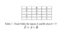
circuit 20 will have a different logical function, depending on this fixed logic value and will result in a variety of different logic relations between the output and the inputs. In other words, the circuit inFIG. 2 performs a logic operation of inputs A and B depending on the logic state of input C. It is also true that the logic operation of inputs B and C depends on the logic state of input A. - When input C has a logic state of ‘1’ (at Vdd supply voltage), the circuit is analyzed for its input to output logic relationship and the result is stated in the truth table of Table 1. It can be found from Table 1 that the output Z is the logical function ‘OR’ of inputs A and B. In logic equation form, this is specified as Z=A+B. A logic symbol representation of Z=A+B is also drawn in
FIG. 3 . When the logic state at input C is ‘0’ (at Vss voltage), the logic relationship of output Z on inputs A and B becomes ‘A AND B bar’. In logic equation form, it is specified as Z=A·B , whereB is the logical inverse of input B. This logic relationship is illustrated in the truth table of Table 2 and its associated logic symbol is drawn inFIG. 4 . - The same analogy can be applied to having input A as the controlling logic state and the circuit performs logic operation on input B and input C. When input A has a logic state of ‘0’ (at Vss voltage), from Table 3 the output Z is the logical function ‘AND’ of inputs B and C. In logic equation form, this is specified as Z=B·C. A logic symbol representation of Z=B·C is drawn in
FIG. 5 . Again, when the logic state at input A is ‘0’ (at Vdd supply voltage), the logic relationship of output Z on inputs B and C becomes ‘B bar OR C’, or in logic equation form, specified as Z=B +C whereB is the logical inverse of input B. This logic relationship and logic symbol are illustrated in Table 4 andFIG. 6 respectively. - Since the actual logic function performed by the circuit in
FIG. 2 can be varied by the logic states of either inputs A or C, which is to say that the circuit inFIG. 2 can be a different logic gate (either an AND gate or OR gate) depending on the logic content at either of its inputs. Further, while the embodiment shown inFIG. 2 comprises two inputs and a control input, using the principles described above, building blocks can be constructed that include additional inputs and/or outputs as desired. -
FIG. 7 illustrates an example of how this bit content can be programmed to change the logic function of the basic logic block ofFIG. 2 . Twocamouflage connectors FIG. 7 connecting to the input C of thebasic logic block 20. Acamouflage connector - In
FIG. 7 , onecamouflage connector 31 connects input C to the node labeled as C1, theother camouflage connector 32 is connected between input C and node labeled as C2. Nodes C1 and C2 can be driven by supply voltages Vdd, Vss, or by other active output signals from other logic cells, or even by the logic block's own output Z as a feedback signal. When thetop camouflage connector 32 is programmed to be a connection with node C2 connected to Vdd, while thebottom camouflage connector 31 is programmed to be in isolation, input C will receive a logic state of ‘1’ and the logic block performs as an ‘OR’ gate of inputs A and B. Node C1 in this case can be connected to any signal since thebottom camouflage connector 31 is isolated. - If the top camouflage connector (32) is programmed to be isolated, while the
bottom camouflage connector 31 is programmed to be a connector with node C1 connected to Vss, the logic state at input C is ‘0’ and the logic block performs the logic function of ‘A AND B bar’ (Z=A·B ). Node C2 in this case can be connected to any signal since the top camouflage connector is isolated. - An example from U.S. Patent Publication 20080079082 is shown in
FIG. 8 . The top drawing inFIG. 8 shows a connection implemented with an N-type extension implant, also called an NLDD (N-type Lightly Doped Drain) implant. To make such a camouflage connector, a silicide window is opened over a PN junction in an active silicon area to avoid a direct short of the PN junction through Silicide. Silicide, sometimes called Salicide (Self-aligned Silicide), is a metallic silicon compound formed by depositing a thin layer of metal (e.g. Titanium) on the silicon surface for the purpose of reducing the sheet resistance of the silicon implanted regions. When the center part of this PN junction with silicide window is implanted with NLDD implant, the two terminals of the PN junction will be shorted, due to the conduction path from N+ region to NLDD region and further from NLDD region to P+ region via the silicide on top. The NLDD implant is one of the standard implants in the CMOS fabrication process. It is a lighter doped implant compared to the source and drain N+/P+ implants. Its function is to reduce the short channel effect of the CMOS N-type devices. The P-type extension, or PLDD implant, is the similar kind of implant for the P-type device in CMOS fabrication. Switching the NLDD in the top structure ofFIG. 8 to PLDD implant will turn the structure into isolation as a reverse biased PN junction. This is shown in the bottom drawing ofFIG. 8 . The presence of field oxide (F.O.) is to isolate the camouflage connectors from other active circuits. Since NLDD and PLDD implants are lighter in concentration and shallower in depth compared to the source and drain N+/P+ implants, reverse engineers will find them difficult to differentiate when they are located next to the heavy doped N+/P+ region. It is favorable to use as many as possible of the different techniques to implement camouflage connectors, because the greater the variety of camouflage connectors, the more difficult it will be to reverse engineer an ASIC designed with these camouflage connectors. - Logic cells of different functions can be built by combining the basic
logic building block 20 ofFIG. 2 together with variety of camouflage connector structures (including the one shown inFIG. 8 ). A secure CMOS library described in this invention is a collection of such logic cells. Groups of various logic cells in the secure CMOS library are designed with the same building block (such as is shown inFIG. 2 ) so they have identical circuits and physical layout. An ASIC, designed with this secure library will have a large number of identical logic building blocks with identical physical appearance. This prevents reverse engineers from relying on the appearance of the logic gates to identify their logic functions. - A secure CMOS logic cell library requires various logic elements. In general, these elements can be categorized into random logic gates including but not limited to AND gates, OR gates, inverters and buffers, and sequential logic elements of latches and flip-flops. For random logic gates, De Morgan's law can be used to synthesize any random logic function with a minimum set of logic gates of 2-input AND gates, 2-input OR gates and inverters. For sequential logic cells, the fundamental elements are one-bit latches and D-type flip-flops.
- A minimum logic library can have minimum logic gates of a 2-input AND, a 2-input OR, an inverter and also a 1-bit latch and a D-type flip flop. Although not necessarily efficient, theoretically this minimum library can generate any logic combination.
- In order to have a more efficient and optimized logic implementation, a logic library with more cells should be used. The basic
logical building block 20 can be used to implement other logic elements as follows. We have already described in the above text how a 2-input AND gate and a 2-input OR gate can be implemented using the basiclogic block circuit 20. Since inverting capability may be needed in a logic cell library, it can be noted that in the realization of logic gates depicted inFIG. 4 andFIG. 6 , input B is inverted before going through logic operation with input A or input C. Therefore, the basiclogic block circuit 20 includes inverting capability. - An individual inverter can also be implemented with the same building block in
FIG. 2 .FIG. 9 shows how an inverter of input B can be accomplished. When input A is at logic ‘0’ (voltage at Vss) and input C is at logic ‘1’ (voltage at Vdd), the circuit inFIG. 9 works as an inverter of input B. The same circuit inFIG. 9 with input A at logic ‘1’ (Vdd voltage) and input C at logic ‘0’ (Vss voltage) will become a non inverting buffer of input B. Multiple camouflage connectors are used here in the programming of logic states at input A and inputC. Camouflage connectors - For sequential logic, a latch can also be made with the basic building block in
FIG. 2 together with a camouflage connector connecting input C to the output Z. This is depicted inFIG. 10 . Whencamouflage connector 31 inFIG. 10 is programmed to be ‘on’ (conduction) whilecamouflage connector 32 is ‘off’ (isolation), the circuit is a latch with input at A and output at Z. Input B is the latch clock of this circuit. If the programming of thecamouflage connectors FIG. 10 is the same asFIG. 3 which is an OR gate of input A and B. Although circuit inFIG. 10 has a unique connection from the output Z to thecamouflage connector 31, reverse engineering can not rely on that information to assume its specific logic function because its actual logic function is still determined by the on and off of the camouflage connectors. This is a critical consideration when applying the teaching of this description to design logic library cells. The goal is to maintain enough possibilities of uncertainty for every logic cell design so no single cell has any unique signature for recognition in a reverse engineering attempt. - A master and slave D-type Flip-flop can be realized by two of the above latches connected in series.
FIG. 11 is the diagram for such a D-type Flip flop with input A being the D input of the flip-flop and output Z being the output Q of the flip-flop. Input B1 and input B will be equivalent to the Clock and the Clock bar of the flip flop respectively. Bothcamouflage connectors 31 inFIG. 11 are in conduction and bothcamouflage connectors 32 are in isolation. This invention is not limited to the implementation of the above described logic cells. Other logic functions like the Multiplexer, Exclusive OR, Adders, etc. can also be implemented in a similar fashion with the basic building block of this invention. - With some minor modifications of the basic building block, for example inverters at inputs A, B, C and output Z are replaced with logic gates, more combinations of logic functions can be further realized.
FIG. 12 demonstrates the example of a new logic functional block when the inverter at input A is replaced with a NOR gate. Although the circuit of the building block inFIG. 12 is different from the original basic building block inFIG. 2 , its actual logic function is still determined by the logic state of input C. It can be derived by analyzing the circuit when input C is at logic ‘0’, the logic function of output Z equals to A1+A2+B. When input C is at logic ‘1’, the logic function of output Z equals to Z=(A1+A2)·B . Similarly, logic gates of other functions can replace the other input inverters or the output inverter to create different building blocks for more complex logic functions. - A practical secure logic cell library implemented by this invention can have more than one basic building block to optimize the effectiveness of logic synthesizing in a real ASIC design. A practical library may also have cells of the same logic function but different driving capabilities due to the requirement of different loading conditions in the real ASIC design. In this invention, different driving capabilities can be achieved by modifying the basic building block with different sizes of the inverter at output Z 24 (
FIG. 2 ). - In the practice of a modern ASIC design, the whole ASIC logic function is written in high-level hardware description language like the VHDL or VERILOG. It will be simulated and verified with a VHDL/VERILOG logic simulator. The final ASIC design which is still in VHDL or VERILOG language will be read into a logic synthesizer (e.g. SYNOPSYS DESIGN COMPILER) to synthesize the logic implementation and generate a connection netlist (schematics) of logic cells based on a target logic cell library. It is not necessary and not possible for a library to have logic cells of all possible logic functions, instead De Morgan's law will be extensively used in the logic-synthesizing step to map the design to the available functions. It was mentioned earlier that a minimum logic library can have only one 2-input AND gate, one 2-input OR gate, one Inverter, one single bit latch and a D-type flip flop. A logic synthesizer can even use such a library with the minimum number of logic elements to create a netlist of a real ASIC design. In reality, it will be more effective and efficient meeting the operational speed and silicon area requirements of the ASIC for a logic library to have more logic functional cells. A practical library usually contains several hundred of cells with multiple drive capabilities. A real logic cell library may only have 20-50 different types of logic functions.
- An ASIC designed with a logic library developed with techniques described in this invention will contain hundred of thousands or even millions of a few slightly different basic building blocks with also millions of all sorts of camouflage connectors. There is no obvious signature of any kind to give any clue of each logic cell's actual function. Reverse engineering can not rely on simple optical or electron microscope images to extract the actual ASIC design. While it is true that the connection or isolation of a camouflage connector can still be identified by direct manual probing, there has not yet been an automatic and speedy direct probing mechanism that can produce accurate probing results for millions of microscopic camouflage connectors within a reasonable amount of time. Direct probing of every camouflage connector in an ASIC designed with a library from this invention is impractical. Such an ASIC can strongly resist a reverse engineering attack.
-
FIG. 13 is a diagram illustrating an exemplary computer system 100 that could be used to implement elements of the present invention. Thecomputer 1302 comprises a generalpurpose hardware processor 1304A and/or a specialpurpose hardware processor 1304B (hereinafter alternatively collectively referred to as processor 1304) and amemory 1306, such as random access memory (RAM). Thecomputer 1302 may be coupled to other devices, including input/output (I/O) devices such as akeyboard 1314, amouse device 1316 and aprinter 1328. - In one embodiment, the
computer 1302 operates by the general-purpose processor 1304A performing instructions defined by thecomputer program 1310 under control of anoperating system 1308. Thecomputer program 1310 and/or theoperating system 1308 may be stored in thememory 1306 and may interface with the user and/or other devices to accept input and commands and, based on such input and commands and the instructions defined by thecomputer program 1310 andoperating system 1308 to provide output and results. - Output/results may be presented on the
display 1322 or provided to another device for presentation or further processing or action. In one embodiment, thedisplay 1322 comprises a liquid crystal display (LCD) having a plurality of separately addressable pixels formed by liquid crystals. Each pixel of thedisplay 1322 changes to an opaque or translucent state to form a part of the image on the display in response to the data or information generated by the processor 1304 from the application of the instructions of thecomputer program 1310 and/oroperating system 1308 to the input and commands.Other display 1322 types also include picture elements that change state in order to create the image presented on thedisplay 1322. The image may be provided through a graphical user interface (GUI)module 1318A. Although theGUI module 1318A is depicted as a separate module, the instructions performing the GUI functions can be resident or distributed in theoperating system 1308, thecomputer program 1310, or implemented with special purpose memory and processors. - Some or all of the operations performed by the
computer 1302 according to thecomputer program 1310 instructions may be implemented in aspecial purpose processor 1304B. In this embodiment, some or all of thecomputer program 1310 instructions may be implemented via firmware instructions stored in a read only memory (ROM), a programmable read only memory (PROM) or flash memory within thespecial purpose processor 1304B or inmemory 1306. Thespecial purpose processor 1304B may also be hardwired through circuit design to perform some or all of the operations to implement the present invention. Further, thespecial purpose processor 1304B may be a hybrid processor, which includes dedicated circuitry for performing a subset of functions, and other circuits for performing more general functions such as responding to computer program instructions. In one embodiment, the special purpose processor is an application specific integrated circuit (ASIC). - The
computer 1302 may also implement acompiler 1312 which allows anapplication program 1310 written in a programming language such as COBOL, C++, FORTRAN, or other language to be translated into processor 1304 readable code. After completion, the application orcomputer program 1310 accesses and manipulates data accepted from I/O devices and stored in thememory 1306 of thecomputer 1302 using the relationships and logic that was generated using thecompiler 1312. - The
computer 1302 also optionally comprises an external communication device such as a modem, satellite link, Ethernet card, or other device for accepting input from and providing output to other computers. - In one embodiment, instructions implementing the
operating system 1308, thecomputer program 1310, and/or thecompiler 1312 are tangibly embodied in a computer-readable medium, e.g.,data storage device 1320, which could include one or more fixed or removable data storage devices, such as a zip drive,floppy disc drive 1324, hard drive, CD-ROM drive, tape drive, or a flash drive. Further, theoperating system 1308 and thecomputer program 1310 are comprised of computer program instructions which, when accessed, read and executed by thecomputer 1302, causes thecomputer 1302 to perform the steps necessary to implement and/or use the present invention or to load the program of instructions into a memory, thus creating a special purpose data structure causing the computer to operate as a specially programmed computer executing the method steps described herein.Computer program 1310 and/or operating instructions may also be tangibly embodied inmemory 1306 and/ordata communications devices 1330, thereby making a computer program product or article of manufacture according to the invention. As such, the terms “article of manufacture,” “program storage device” and “computer program product” or “computer readable storage device” as used herein are intended to encompass a computer program accessible from any computer readable device or media. - Of course, those skilled in the art will recognize that any combination of the above components, or any number of different components, peripherals, and other devices, may be used with the
computer 1302. - Although the term “computer” is referred to herein, it is understood that the computer may include portable devices such as cellphones, portable MP3 players, video game consoles, notebook computers, pocket computers, or any other device with suitable processing, communication, and input/output capability.
- The foregoing description of the preferred embodiment of the invention has been presented for the purposes of illustration and description. It is not intended to be exhaustive or to limit the invention to the precise form disclosed. Many modifications and variations are possible in light of the above teaching. It is intended that the scope of the invention be limited not by this detailed description, but rather by the claims appended hereto. The above specification, examples and data provide a complete description of the manufacture and use of the composition of the invention. Since many embodiments of the invention can be made without departing from the spirit and scope of the invention, the invention resides in the claims hereinafter appended.
Claims (18)
Priority Applications (1)
| Application Number | Priority Date | Filing Date | Title |
|---|---|---|---|
| US12/786,205 US8111089B2 (en) | 2009-05-28 | 2010-05-24 | Building block for a secure CMOS logic cell library |
Applications Claiming Priority (2)
| Application Number | Priority Date | Filing Date | Title |
|---|---|---|---|
| US18193009P | 2009-05-28 | 2009-05-28 | |
| US12/786,205 US8111089B2 (en) | 2009-05-28 | 2010-05-24 | Building block for a secure CMOS logic cell library |
Publications (2)
| Publication Number | Publication Date |
|---|---|
| US20100301903A1 true US20100301903A1 (en) | 2010-12-02 |
| US8111089B2 US8111089B2 (en) | 2012-02-07 |
Family
ID=43219511
Family Applications (1)
| Application Number | Title | Priority Date | Filing Date |
|---|---|---|---|
| US12/786,205 Expired - Fee Related US8111089B2 (en) | 2009-05-28 | 2010-05-24 | Building block for a secure CMOS logic cell library |
Country Status (1)
| Country | Link |
|---|---|
| US (1) | US8111089B2 (en) |
Cited By (13)
| Publication number | Priority date | Publication date | Assignee | Title |
|---|---|---|---|---|
| WO2013118119A1 (en) * | 2012-02-09 | 2013-08-15 | B.G. Negev Technologies & Applications Ltd. | Design of dual mode logic circuits |
| WO2014070216A1 (en) * | 2012-10-30 | 2014-05-08 | Static Control Components, Inc. | Semiconductor device having features to prevent reverse engineering |
| US8901965B2 (en) | 2011-08-03 | 2014-12-02 | Ben-Gurion University Of The Negev Research And Development Authority | Device and method for dual-mode logic |
| US8975748B1 (en) | 2011-06-07 | 2015-03-10 | Secure Silicon Layer, Inc. | Semiconductor device having features to prevent reverse engineering |
| US9218511B2 (en) | 2011-06-07 | 2015-12-22 | Verisiti, Inc. | Semiconductor device having features to prevent reverse engineering |
| US20160034628A1 (en) * | 2013-03-14 | 2016-02-04 | New York University | System, method and computer-accessible medium for providing secure split manufacturing |
| US20160224407A1 (en) * | 2013-09-11 | 2016-08-04 | New York University | System, method and computer-accessible medium for fault analysis driven selection of logic gates to be camouflaged |
| US9437555B2 (en) | 2011-06-07 | 2016-09-06 | Verisiti, Inc. | Semiconductor device having features to prevent reverse engineering |
| US9479176B1 (en) * | 2013-12-09 | 2016-10-25 | Rambus Inc. | Methods and circuits for protecting integrated circuits from reverse engineering |
| US20180341737A1 (en) * | 2009-02-24 | 2018-11-29 | Inside Secure | Secure logic locking and configuration with camouflaged programmable micro netlists |
| US10476883B2 (en) * | 2012-03-02 | 2019-11-12 | Inside Secure | Signaling conditional access system switching and key derivation |
| US10574237B2 (en) | 2009-02-24 | 2020-02-25 | Verimatrix | Physically unclonable camouflage structure and methods for fabricating same |
| US10990580B2 (en) | 2017-10-25 | 2021-04-27 | New York University | System, method and computer-accessible medium for stripped-functionality logic locking |
Families Citing this family (14)
| Publication number | Priority date | Publication date | Assignee | Title |
|---|---|---|---|---|
| US8510700B2 (en) * | 2009-02-24 | 2013-08-13 | Syphermedia International, Inc. | Method and apparatus for camouflaging a standard cell based integrated circuit with micro circuits and post processing |
| WO2012070821A2 (en) * | 2010-11-22 | 2012-05-31 | 한양대학교 산학협력단 | Layout library of flip-flop circuit |
| US9806881B2 (en) | 2014-06-27 | 2017-10-31 | Infineon Technologies Ag | Cryptographic processor, method for implementing a cryptographic processor and key generation circuit |
| US9548737B1 (en) | 2015-07-17 | 2017-01-17 | Infineon Technologies Ag | Method for manufacturing a digital circuit and digital circuit |
| US9496872B1 (en) * | 2015-07-17 | 2016-11-15 | Infineon Technologies Ag | Method for manufacturing a digital circuit and digital circuit |
| WO2017123305A2 (en) * | 2015-10-22 | 2017-07-20 | Drexel University | Reduced overhead gate level logic encryption |
| CN106330174B (en) * | 2016-08-16 | 2019-02-12 | 深圳市华星光电技术有限公司 | The electronic device of CMOS inverter and the application CMOS inverter |
| US10642947B2 (en) | 2016-09-06 | 2020-05-05 | New York University | System, method and computer-accessible medium providing secure integrated circuit camouflaging for minterm protection |
| US10262956B2 (en) | 2017-02-27 | 2019-04-16 | Cisco Technology, Inc. | Timing based camouflage circuit |
| US11831309B2 (en) * | 2018-04-20 | 2023-11-28 | Texas Instruments Incorporated | Stress reduction on stacked transistor circuits |
| US11626875B2 (en) * | 2018-04-20 | 2023-04-11 | Texas Instruments Incorporated | Stress reduction on stacked transistor circuits |
| US11695011B2 (en) | 2018-05-02 | 2023-07-04 | Nanyang Technological University | Integrated circuit layout cell, integrated circuit layout arrangement, and methods of forming the same |
| US10923596B2 (en) | 2019-03-08 | 2021-02-16 | Rambus Inc. | Camouflaged FinFET and method for producing same |
| DE102019123555B4 (en) | 2019-09-03 | 2022-12-01 | Infineon Technologies Ag | PHYSICALLY OBFUSCED CIRCUIT |
Citations (37)
| Publication number | Priority date | Publication date | Assignee | Title |
|---|---|---|---|---|
| US5636133A (en) * | 1995-05-19 | 1997-06-03 | International Business Machines Corporation | Efficient generation of fill shapes for chips and packages |
| US5783846A (en) * | 1995-09-22 | 1998-07-21 | Hughes Electronics Corporation | Digital circuit with transistor geometry and channel stops providing camouflage against reverse engineering |
| US5866933A (en) * | 1992-07-31 | 1999-02-02 | Hughes Electronics Corporation | Integrated circuit security system and method with implanted interconnections |
| US5973375A (en) * | 1997-06-06 | 1999-10-26 | Hughes Electronics Corporation | Camouflaged circuit structure with step implants |
| US6117762A (en) * | 1999-04-23 | 2000-09-12 | Hrl Laboratories, Llc | Method and apparatus using silicide layer for protecting integrated circuits from reverse engineering |
| US6305000B1 (en) * | 1999-06-15 | 2001-10-16 | International Business Machines Corporation | Placement of conductive stripes in electronic circuits to satisfy metal density requirements |
| US6351172B1 (en) * | 2000-02-29 | 2002-02-26 | Dmel Inc. | High-speed output driver with an impedance adjustment scheme |
| US20020096744A1 (en) * | 2001-01-24 | 2002-07-25 | Hrl Laboratories, Llc | Integrated circuits protected against reverse engineering and method for fabricating the same using etched passivation openings in integrated circuits |
| US20020096776A1 (en) * | 2001-01-24 | 2002-07-25 | Hrl Laboratories, Llc | Integrated circuits protected against reverse engineering and method for fabricating the same using an apparent metal contact line terminating on field oxide |
| US6459629B1 (en) * | 2001-05-03 | 2002-10-01 | Hrl Laboratories, Llc | Memory with a bit line block and/or a word line block for preventing reverse engineering |
| US6467074B1 (en) * | 2000-03-21 | 2002-10-15 | Ammocore Technology, Inc. | Integrated circuit architecture with standard blocks |
| US20040061186A1 (en) * | 2002-09-27 | 2004-04-01 | Lap-Wai Chow | Conductive channel pseudo block process and circuit to inhibit reverse engineering |
| US6740942B2 (en) * | 2001-06-15 | 2004-05-25 | Hrl Laboratories, Llc. | Permanently on transistor implemented using a double polysilicon layer CMOS process with buried contact |
| US6748579B2 (en) * | 2002-08-30 | 2004-06-08 | Lsi Logic Corporation | Method of using filler metal for implementing changes in an integrated circuit design |
| US20040130349A1 (en) * | 2002-08-29 | 2004-07-08 | Arkadiy Morgenshtein | Logic circuit and method of logic circuit design |
| US20040144998A1 (en) * | 2002-12-13 | 2004-07-29 | Lap-Wai Chow | Integrated circuit modification using well implants |
| US6774413B2 (en) * | 2001-06-15 | 2004-08-10 | Hrl Laboratories, Llc | Integrated circuit structure with programmable connector/isolator |
| US6791191B2 (en) * | 2001-01-24 | 2004-09-14 | Hrl Laboratories, Llc | Integrated circuits protected against reverse engineering and method for fabricating the same using vias without metal terminations |
| US6815816B1 (en) * | 2000-10-25 | 2004-11-09 | Hrl Laboratories, Llc | Implanted hidden interconnections in a semiconductor device for preventing reverse engineering |
| US6897535B2 (en) * | 2002-05-14 | 2005-05-24 | Hrl Laboratories, Llc | Integrated circuit with reverse engineering protection |
| US20050140389A1 (en) * | 2003-11-21 | 2005-06-30 | Infineon Technologies Ag | Logic basic cell and logic basic cell arrangement |
| US6924552B2 (en) * | 2002-10-21 | 2005-08-02 | Hrl Laboratories, Llc | Multilayered integrated circuit with extraneous conductive traces |
| US6944843B2 (en) * | 2003-08-05 | 2005-09-13 | Bae Systems, Information And Electronic Systems Integration, Inc. | Method for providing a cell-based ASIC device with multiple power supply voltages |
| US20050230787A1 (en) * | 2004-04-19 | 2005-10-20 | Hrl Laboratories, Llc. | Covert transformation of transistor properties as a circuit protection method |
| US6979606B2 (en) * | 2002-11-22 | 2005-12-27 | Hrl Laboratories, Llc | Use of silicon block process step to camouflage a false transistor |
| US7009443B2 (en) * | 2004-06-07 | 2006-03-07 | Standard Microsystems Corporation | Method and circuit for fuse programming and endpoint detection |
| US7042752B2 (en) * | 2002-12-13 | 2006-05-09 | Renesas Technology Corp. | IC card system using photo-detectors for protection |
| US7170317B2 (en) * | 2003-05-23 | 2007-01-30 | Arithmatica Limited | Sum bit generation circuit |
| US7279936B2 (en) * | 2003-12-08 | 2007-10-09 | Infineon Technologies Ag | Logic basic cell, logic basic cell arrangement and logic device |
| US7328419B2 (en) * | 2002-11-19 | 2008-02-05 | Cadence Design Systems, Inc. | Place and route tool that incorporates a metal-fill mechanism |
| US7383521B2 (en) * | 2002-06-07 | 2008-06-03 | Cadence Design Systems, Inc. | Characterization and reduction of variation for integrated circuits |
| US20080237644A1 (en) * | 2007-03-30 | 2008-10-02 | Stmicroelectronics, Inc. | Spatially aware drive strength dependent die size independent combinatorial spare cell insertion manner and related system and method |
| US20080282208A1 (en) * | 2007-01-11 | 2008-11-13 | Brent Alan Anderson | Integrated Circuit Having Anti-counterfeiting Measures |
| US20100218158A1 (en) * | 2009-02-24 | 2010-08-26 | Syphermedia International, Inc. | Method and apparatus for camouflaging a standard cell based integrated circuit |
| US20100231263A1 (en) * | 2005-02-16 | 2010-09-16 | Alexander Fish | Logic Circuit and Method of Logic Circuit Design |
| US7844936B2 (en) * | 2007-08-22 | 2010-11-30 | Infineon Technologies Ag | Method of making an integrated circuit having fill structures |
| US7895548B2 (en) * | 2007-10-26 | 2011-02-22 | Synopsys, Inc. | Filler cells for design optimization in a place-and-route system |
-
2010
- 2010-05-24 US US12/786,205 patent/US8111089B2/en not_active Expired - Fee Related
Patent Citations (48)
| Publication number | Priority date | Publication date | Assignee | Title |
|---|---|---|---|---|
| US5866933A (en) * | 1992-07-31 | 1999-02-02 | Hughes Electronics Corporation | Integrated circuit security system and method with implanted interconnections |
| US6613661B1 (en) * | 1992-07-31 | 2003-09-02 | Hughes Electronics Corporation | Process for fabricating secure integrated circuit |
| US6294816B1 (en) * | 1992-07-31 | 2001-09-25 | Hughes Electronics Corporation | Secure integrated circuit |
| US5636133A (en) * | 1995-05-19 | 1997-06-03 | International Business Machines Corporation | Efficient generation of fill shapes for chips and packages |
| US5783846A (en) * | 1995-09-22 | 1998-07-21 | Hughes Electronics Corporation | Digital circuit with transistor geometry and channel stops providing camouflage against reverse engineering |
| US5930663A (en) * | 1995-09-22 | 1999-07-27 | Hughes Electronics Corporation | Digital circuit with transistor geometry and channel stops providing camouflage against reverse engineering |
| US6064110A (en) * | 1995-09-22 | 2000-05-16 | Hughes Electronics Corporation | Digital circuit with transistor geometry and channel stops providing camouflage against reverse engineering |
| US5973375A (en) * | 1997-06-06 | 1999-10-26 | Hughes Electronics Corporation | Camouflaged circuit structure with step implants |
| US6117762A (en) * | 1999-04-23 | 2000-09-12 | Hrl Laboratories, Llc | Method and apparatus using silicide layer for protecting integrated circuits from reverse engineering |
| US6305000B1 (en) * | 1999-06-15 | 2001-10-16 | International Business Machines Corporation | Placement of conductive stripes in electronic circuits to satisfy metal density requirements |
| US6351172B1 (en) * | 2000-02-29 | 2002-02-26 | Dmel Inc. | High-speed output driver with an impedance adjustment scheme |
| US6467074B1 (en) * | 2000-03-21 | 2002-10-15 | Ammocore Technology, Inc. | Integrated circuit architecture with standard blocks |
| US6815816B1 (en) * | 2000-10-25 | 2004-11-09 | Hrl Laboratories, Llc | Implanted hidden interconnections in a semiconductor device for preventing reverse engineering |
| US20020096744A1 (en) * | 2001-01-24 | 2002-07-25 | Hrl Laboratories, Llc | Integrated circuits protected against reverse engineering and method for fabricating the same using etched passivation openings in integrated circuits |
| US20020096776A1 (en) * | 2001-01-24 | 2002-07-25 | Hrl Laboratories, Llc | Integrated circuits protected against reverse engineering and method for fabricating the same using an apparent metal contact line terminating on field oxide |
| US6791191B2 (en) * | 2001-01-24 | 2004-09-14 | Hrl Laboratories, Llc | Integrated circuits protected against reverse engineering and method for fabricating the same using vias without metal terminations |
| US6459629B1 (en) * | 2001-05-03 | 2002-10-01 | Hrl Laboratories, Llc | Memory with a bit line block and/or a word line block for preventing reverse engineering |
| US6940764B2 (en) * | 2001-05-03 | 2005-09-06 | Hrl Laboratories Llc | Memory with a bit line block and/or a word line block for preventing reverse engineering |
| US6740942B2 (en) * | 2001-06-15 | 2004-05-25 | Hrl Laboratories, Llc. | Permanently on transistor implemented using a double polysilicon layer CMOS process with buried contact |
| US6919600B2 (en) * | 2001-06-15 | 2005-07-19 | Hrl Laboratories, Llc | Permanently on transistor implemented using a double polysilicon layer CMOS process with buried contact |
| US6893916B2 (en) * | 2001-06-15 | 2005-05-17 | Hrl Laboratories, Llc | Programmable connector/isolator and double polysilicon layer CMOS process with buried contact using the same |
| US6774413B2 (en) * | 2001-06-15 | 2004-08-10 | Hrl Laboratories, Llc | Integrated circuit structure with programmable connector/isolator |
| US6897535B2 (en) * | 2002-05-14 | 2005-05-24 | Hrl Laboratories, Llc | Integrated circuit with reverse engineering protection |
| US7008873B2 (en) * | 2002-05-14 | 2006-03-07 | Hrl Laboratories, Llc | Integrated circuit with reverse engineering protection |
| US20050161748A1 (en) * | 2002-05-14 | 2005-07-28 | Hrl Laboratories, Llc | Integrated circuit with reverse engineering protection |
| US7383521B2 (en) * | 2002-06-07 | 2008-06-03 | Cadence Design Systems, Inc. | Characterization and reduction of variation for integrated circuits |
| US20040130349A1 (en) * | 2002-08-29 | 2004-07-08 | Arkadiy Morgenshtein | Logic circuit and method of logic circuit design |
| US20070261015A1 (en) * | 2002-08-29 | 2007-11-08 | Technion Research & Development Foundation Ltd. | Logic circuit and method of logic circuit design |
| US6748579B2 (en) * | 2002-08-30 | 2004-06-08 | Lsi Logic Corporation | Method of using filler metal for implementing changes in an integrated circuit design |
| US20040061186A1 (en) * | 2002-09-27 | 2004-04-01 | Lap-Wai Chow | Conductive channel pseudo block process and circuit to inhibit reverse engineering |
| US7049667B2 (en) * | 2002-09-27 | 2006-05-23 | Hrl Laboratories, Llc | Conductive channel pseudo block process and circuit to inhibit reverse engineering |
| US6924552B2 (en) * | 2002-10-21 | 2005-08-02 | Hrl Laboratories, Llc | Multilayered integrated circuit with extraneous conductive traces |
| US7328419B2 (en) * | 2002-11-19 | 2008-02-05 | Cadence Design Systems, Inc. | Place and route tool that incorporates a metal-fill mechanism |
| US6979606B2 (en) * | 2002-11-22 | 2005-12-27 | Hrl Laboratories, Llc | Use of silicon block process step to camouflage a false transistor |
| US20040144998A1 (en) * | 2002-12-13 | 2004-07-29 | Lap-Wai Chow | Integrated circuit modification using well implants |
| US7042752B2 (en) * | 2002-12-13 | 2006-05-09 | Renesas Technology Corp. | IC card system using photo-detectors for protection |
| US7170317B2 (en) * | 2003-05-23 | 2007-01-30 | Arithmatica Limited | Sum bit generation circuit |
| US6944843B2 (en) * | 2003-08-05 | 2005-09-13 | Bae Systems, Information And Electronic Systems Integration, Inc. | Method for providing a cell-based ASIC device with multiple power supply voltages |
| US20050140389A1 (en) * | 2003-11-21 | 2005-06-30 | Infineon Technologies Ag | Logic basic cell and logic basic cell arrangement |
| US7279936B2 (en) * | 2003-12-08 | 2007-10-09 | Infineon Technologies Ag | Logic basic cell, logic basic cell arrangement and logic device |
| US20050230787A1 (en) * | 2004-04-19 | 2005-10-20 | Hrl Laboratories, Llc. | Covert transformation of transistor properties as a circuit protection method |
| US7009443B2 (en) * | 2004-06-07 | 2006-03-07 | Standard Microsystems Corporation | Method and circuit for fuse programming and endpoint detection |
| US20100231263A1 (en) * | 2005-02-16 | 2010-09-16 | Alexander Fish | Logic Circuit and Method of Logic Circuit Design |
| US20080282208A1 (en) * | 2007-01-11 | 2008-11-13 | Brent Alan Anderson | Integrated Circuit Having Anti-counterfeiting Measures |
| US20080237644A1 (en) * | 2007-03-30 | 2008-10-02 | Stmicroelectronics, Inc. | Spatially aware drive strength dependent die size independent combinatorial spare cell insertion manner and related system and method |
| US7844936B2 (en) * | 2007-08-22 | 2010-11-30 | Infineon Technologies Ag | Method of making an integrated circuit having fill structures |
| US7895548B2 (en) * | 2007-10-26 | 2011-02-22 | Synopsys, Inc. | Filler cells for design optimization in a place-and-route system |
| US20100218158A1 (en) * | 2009-02-24 | 2010-08-26 | Syphermedia International, Inc. | Method and apparatus for camouflaging a standard cell based integrated circuit |
Cited By (24)
| Publication number | Priority date | Publication date | Assignee | Title |
|---|---|---|---|---|
| US10574237B2 (en) | 2009-02-24 | 2020-02-25 | Verimatrix | Physically unclonable camouflage structure and methods for fabricating same |
| US11264990B2 (en) | 2009-02-24 | 2022-03-01 | Rambus Inc. | Physically unclonable camouflage structure and methods for fabricating same |
| US11163930B2 (en) | 2009-02-24 | 2021-11-02 | Rambus Inc. | Secure logic locking and configuration with camouflaged programmable micro netlists |
| US10691860B2 (en) * | 2009-02-24 | 2020-06-23 | Rambus Inc. | Secure logic locking and configuration with camouflaged programmable micro netlists |
| US20180341737A1 (en) * | 2009-02-24 | 2018-11-29 | Inside Secure | Secure logic locking and configuration with camouflaged programmable micro netlists |
| US9972585B2 (en) | 2011-06-07 | 2018-05-15 | Verisiti, Inc. | Semiconductor device having features to prevent reverse engineering |
| US8975748B1 (en) | 2011-06-07 | 2015-03-10 | Secure Silicon Layer, Inc. | Semiconductor device having features to prevent reverse engineering |
| US9218511B2 (en) | 2011-06-07 | 2015-12-22 | Verisiti, Inc. | Semiconductor device having features to prevent reverse engineering |
| US9972398B2 (en) | 2011-06-07 | 2018-05-15 | Verisiti, Inc. | Semiconductor device having features to prevent reverse engineering |
| US9287879B2 (en) | 2011-06-07 | 2016-03-15 | Verisiti, Inc. | Semiconductor device having features to prevent reverse engineering |
| US9437555B2 (en) | 2011-06-07 | 2016-09-06 | Verisiti, Inc. | Semiconductor device having features to prevent reverse engineering |
| US9430598B2 (en) | 2011-08-03 | 2016-08-30 | Bar-Ilan University | Dual mode logic circuits |
| US8901965B2 (en) | 2011-08-03 | 2014-12-02 | Ben-Gurion University Of The Negev Research And Development Authority | Device and method for dual-mode logic |
| WO2013118119A1 (en) * | 2012-02-09 | 2013-08-15 | B.G. Negev Technologies & Applications Ltd. | Design of dual mode logic circuits |
| US10476883B2 (en) * | 2012-03-02 | 2019-11-12 | Inside Secure | Signaling conditional access system switching and key derivation |
| CN105324940A (en) * | 2012-10-30 | 2016-02-10 | 威瑞斯蒂公司 | Semiconductor device having features to prevent reverse engineering |
| CN110783329A (en) * | 2012-10-30 | 2020-02-11 | 威瑞斯蒂公司 | Semiconductor device having reverse engineering prevention feature |
| WO2014070216A1 (en) * | 2012-10-30 | 2014-05-08 | Static Control Components, Inc. | Semiconductor device having features to prevent reverse engineering |
| US10423749B2 (en) * | 2013-03-14 | 2019-09-24 | New York University | System, method and computer-accessible medium for providing secure split manufacturing |
| US20160034628A1 (en) * | 2013-03-14 | 2016-02-04 | New York University | System, method and computer-accessible medium for providing secure split manufacturing |
| US10073728B2 (en) * | 2013-09-11 | 2018-09-11 | New York University | System, method and computer-accessible medium for fault analysis driven selection of logic gates to be camouflaged |
| US20160224407A1 (en) * | 2013-09-11 | 2016-08-04 | New York University | System, method and computer-accessible medium for fault analysis driven selection of logic gates to be camouflaged |
| US9479176B1 (en) * | 2013-12-09 | 2016-10-25 | Rambus Inc. | Methods and circuits for protecting integrated circuits from reverse engineering |
| US10990580B2 (en) | 2017-10-25 | 2021-04-27 | New York University | System, method and computer-accessible medium for stripped-functionality logic locking |
Also Published As
| Publication number | Publication date |
|---|---|
| US8111089B2 (en) | 2012-02-07 |
Similar Documents
| Publication | Publication Date | Title |
|---|---|---|
| US8111089B2 (en) | Building block for a secure CMOS logic cell library | |
| Wang et al. | New efficient designs for XOR and XNOR functions on the transistor level | |
| JP4637512B2 (en) | Semiconductor integrated circuit device | |
| US20150311202A1 (en) | Semiconductor chip | |
| EP1012978B1 (en) | An inverse toggle xor and xnor circuit | |
| US7886250B2 (en) | Reconfigurable integrated circuit | |
| EP3308462B1 (en) | Feedback latch circuit | |
| CN101030766A (en) | Power reducing logic and non-destructive latch circuits and applications | |
| JP3433405B2 (en) | Logic block mixing low threshold voltage MOSFET devices and normal threshold voltage MOSFET devices for deep sub-micron VLSI design | |
| US9071238B2 (en) | Contention-free level converting flip-flops for low-swing clocking | |
| CN105843981B (en) | Circuit design system and semiconductor circuit designed by using the same | |
| US7693701B2 (en) | Structure for a configurable low power high fan-in multiplexer | |
| KR102565236B1 (en) | Memory-type camouflaged logic gate using transistors with different threshold voltages | |
| US11886622B2 (en) | Systems and methods for asynchronous programmable gate array devices | |
| US11575366B2 (en) | Low power flip-flop | |
| Lee et al. | Low power null convention logic circuit design based on DCVSL | |
| US20240029780A1 (en) | Efficient muller c-element implementation for high bit-width asynchronous applications | |
| US6970017B2 (en) | Logic circuit | |
| TW202240455A (en) | Poly-bit cells | |
| Calazans et al. | Robust and energy-efficient hardware: the case for asynchronous design | |
| Hiremath et al. | Alu design using low power GDI standard cells | |
| US20100050148A1 (en) | Method and system for automated schematic diagram conversion to support semiconductor body bias designs | |
| US8266562B2 (en) | Method and system for configurable contacts for implementing different bias designs of an integrated circuit device | |
| US20230418556A1 (en) | Static cmos-based full adder circuits | |
| Tsiolakis et al. | Design, simulation and performance evaluation of a NAND based single-electron 2-4 decoder |
Legal Events
| Date | Code | Title | Description |
|---|---|---|---|
| AS | Assignment |
Owner name: SYPHERMEDIA INTERNATIONAL, INC., CALIFORNIA Free format text: ASSIGNMENT OF ASSIGNORS INTEREST;ASSIGNORS:COCCHI, RONALD P.;BAUKUS, JAMES P.;WANG, BRYAN J.;AND OTHERS;REEL/FRAME:024432/0081 Effective date: 20100520 Owner name: PROMTEK PROGRAMMABLE MEMORY TECHNOLOGY, INC., CALI Free format text: ASSIGNMENT OF ASSIGNORS INTEREST;ASSIGNORS:COCCHI, RONALD P.;BAUKUS, JAMES P.;WANG, BRYAN J.;AND OTHERS;REEL/FRAME:024432/0081 Effective date: 20100520 |
|
| ZAAA | Notice of allowance and fees due |
Free format text: ORIGINAL CODE: NOA |
|
| ZAAB | Notice of allowance mailed |
Free format text: ORIGINAL CODE: MN/=. |
|
| STCF | Information on status: patent grant |
Free format text: PATENTED CASE |
|
| FPAY | Fee payment |
Year of fee payment: 4 |
|
| AS | Assignment |
Owner name: INSIDE SECURE S.A., FRANCE Free format text: ASSIGNMENT OF ASSIGNORS INTEREST;ASSIGNOR:SYPHERMEDIA INTERNATIONAL, INC.;REEL/FRAME:045053/0301 Effective date: 20180123 |
|
| FEPP | Fee payment procedure |
Free format text: ENTITY STATUS SET TO UNDISCOUNTED (ORIGINAL EVENT CODE: BIG.) |
|
| AS | Assignment |
Owner name: GLAS SAS, AS SECURITY AGENT, FRANCE Free format text: SECURITY INTEREST;ASSIGNOR:INSIDE SECURE;REEL/FRAME:048449/0887 Effective date: 20190227 |
|
| MAFP | Maintenance fee payment |
Free format text: PAYMENT OF MAINTENANCE FEE, 8TH YEAR, LARGE ENTITY (ORIGINAL EVENT CODE: M1552); ENTITY STATUS OF PATENT OWNER: LARGE ENTITY Year of fee payment: 8 |
|
| AS | Assignment |
Owner name: VERIMATRIX, FRANCE Free format text: CHANGE OF NAME;ASSIGNOR:INSIDE SECURE;REEL/FRAME:050647/0428 Effective date: 20190624 |
|
| AS | Assignment |
Owner name: VERIMATRIX, FRANCE Free format text: CHANGE OF ADDRESS;ASSIGNOR:VERIMATRIX;REEL/FRAME:050733/0003 Effective date: 20190930 |
|
| AS | Assignment |
Owner name: INSIDE SECURE, FRANCE Free format text: PARTIAL RELEASE OF SECURITY INTEREST IN PATENT COLLATERAL;ASSIGNOR:GLAS SAS, AS AGENT;REEL/FRAME:051076/0306 Effective date: 20191112 |
|
| AS | Assignment |
Owner name: RAMBUS INC., CALIFORNIA Free format text: ASSIGNMENT OF ASSIGNORS INTEREST;ASSIGNOR:VERIMATRIX;REEL/FRAME:051262/0413 Effective date: 20191113 |
|
| FEPP | Fee payment procedure |
Free format text: MAINTENANCE FEE REMINDER MAILED (ORIGINAL EVENT CODE: REM.); ENTITY STATUS OF PATENT OWNER: LARGE ENTITY |
|
| LAPS | Lapse for failure to pay maintenance fees |
Free format text: PATENT EXPIRED FOR FAILURE TO PAY MAINTENANCE FEES (ORIGINAL EVENT CODE: EXP.); ENTITY STATUS OF PATENT OWNER: LARGE ENTITY |
|
| STCH | Information on status: patent discontinuation |
Free format text: PATENT EXPIRED DUE TO NONPAYMENT OF MAINTENANCE FEES UNDER 37 CFR 1.362 |
|
| FP | Lapsed due to failure to pay maintenance fee |
Effective date: 20240207 |