US20110037498A1 - Vlsi layouts of fully connected generalized networks - Google Patents
Vlsi layouts of fully connected generalized networks Download PDFInfo
- Publication number
- US20110037498A1 US20110037498A1 US12/601,275 US60127508A US2011037498A1 US 20110037498 A1 US20110037498 A1 US 20110037498A1 US 60127508 A US60127508 A US 60127508A US 2011037498 A1 US2011037498 A1 US 2011037498A1
- Authority
- US
- United States
- Prior art keywords
- integrated circuit
- links
- stage
- switches
- sub
- Prior art date
- Legal status (The legal status is an assumption and is not a legal conclusion. Google has not performed a legal analysis and makes no representation as to the accuracy of the status listed.)
- Granted
Links
Images
Classifications
-
- G—PHYSICS
- G06—COMPUTING; CALCULATING OR COUNTING
- G06F—ELECTRIC DIGITAL DATA PROCESSING
- G06F30/00—Computer-aided design [CAD]
- G06F30/30—Circuit design
- G06F30/39—Circuit design at the physical level
- G06F30/394—Routing
Definitions
- Multi-stage interconnection networks such as Benes networks and butterfly fat tree networks are widely useful in telecommunications, parallel and distributed computing.
- VLSI layouts, known in the prior art, of these interconnection networks in an integrated circuit are inefficient and complicated.
- VLSI layout The most commonly used VLSI layout in an integrated circuit is based on a two-dimensional grid model comprising only horizontal and vertical tracks.
- An intuitive interconnection network that utilizes two-dimensional grid model is 2D Mesh Network and its variations such as segmented mesh networks.
- routing networks used in VLSI layouts are typically 2D mesh networks and its variations.
- Mesh Networks require large scale cross points typically with a growth rate of O(N 2 ) where N is the number of computing elements, ports, or logic elements depending on the application.
- Multi-stage interconnection with a growth rate of O(N ⁇ log N) requires significantly small number of cross points.
- U.S. Pat. No. 6,185,220 entitled “Grid Layouts of Switching and Sorting Networks” granted to Muthukrishnan et al. describes a VLSI layout using existing VLSI grid model for Benes and Butterfly networks.
- U.S. Pat. No. 6,940,308 entitled “Interconnection Network for a Field Programmable Gate Array” granted to Wong describes a VLSI layout where switches belonging to lower stage of Benes Network are layed out close to the logic cells and switches belonging to higher stages are layed out towards the center of the layout.
- the most intuitive routing network is a network that uses horizontal and vertical links only (the most often used such a network is one of the variations of a 2D Mesh network).
- a direct embedding of a generalized multi-stage network on to a 2D Mesh network is neither simple nor efficient.
- VLSI layouts of generalized multi-stage networks for broadcast, unicast and multicast connections are presented using only horizontal and vertical links
- the VLSI layouts employ shuffle exchange links where outlet links of cross links from switches in a stage in one sub-integrated circuit block are connected to inlet links of switches in the succeeding stage in another sub-integrated circuit block so that said cross links are either vertical links or horizontal and vice versa.
- the sub-integrated circuit blocks are arranged in a hypercube arrangement in a two-dimensional plane.
- the VLSI layouts exploit the benefits of significantly lower cross points, lower signal latency, lower power and full connectivity with significantly fast compilation.
- the embodiments of VLSI layouts are useful in wide target applications such as FPGAs, CPLDs, pSoCs, ASIC placement and route tools, networking applications
- V fold-mlink N, d, s
- FIG. 1C is a diagram 100 C layout of the network V fold-mlink (N, d, s) shown in FIG. 1B , in one embodiment, illustrating the connection links belonging with in each block only.
- FIG. 11 is a diagram 100 I detailed connections of BLOCK 1 _ 2 in the network layout 100 C in one embodiment, illustrating the connection links going in and coming out when the layout 100 C is implementing V(N, d, s) or V fold (N, d, s).
- FIG. 1J is a diagram 100 J detailed connections of BLOCK 1 _ 2 in the network layout 100 C in one embodiment, illustrating the connection links going in and coming out when the layout 100 C is implementing V(N, d, s) or V fold (N, d, s).
- FIG. 1K is a diagram 100 K detailed connections of BLOCK 1 _ 2 in the network layout 100 C in one embodiment, illustrating the connection links going in and coming out when the layout 100 C is implementing V(N, d, s) or V fold (N, d, s).
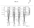
- FIG. 1L is a diagram 100 L detailed connections of BLOCK 1 _ 2 in the network layout 100 C in one embodiment, illustrating the connection links going in and coming out when the layout 100 C is implementing V(N, d, s) or V fold (N, d, s).
- FIG. 2 A 2 is a diagram 200 A 2 of the equivalent symmetrical folded multi-link multi-stage network V fold-mlink (N, d, s) of the network 200 A 1 shown in FIG.
- FIG. 2 A 3 is a diagram 200 A 3 layout of the network V fold-mlink (N, d, s) shown in FIG. 2 A 2 , in one embodiment, illustrating all the connection links.
- FIG. 2 B 2 is a diagram 200 B 2 of the equivalent symmetrical folded multi-link multi-stage network V fold-mlink (N, d, s) of the network 200 B 1 shown in FIG.
- FIG. 2 B 3 is a diagram 200 B 3 layout of the network V fold-mlink (N, d, s) shown in FIG. 2 B 2 , in one embodiment, illustrating the connection links belonging with in each block only.
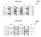
- FIG. 2 C 12 is a diagram 200 C 12 of the equivalent symmetrical folded multi-link multi-stage network V fold-mlink (N, d, s) of the network 200 C 11 shown in FIG.
- FIG. 2 C 21 is a diagram 200 C 21 layout of the network V fold-mlink (N, d, s) shown in FIG. 2 C 12 , in one embodiment, illustrating the connection links belonging with in each block only.
- V fold-mlink N, d, s
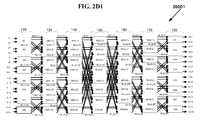
- FIG. 2 D 3 is a diagram 200 D 3 layout of the network V fold-mlink (N, d, s) shown in FIG. 2 D 2 , in one embodiment, illustrating the connection links belonging with in each block only.
- FIG. 3C is a diagram 300 C layout of the network V hcube (N, d, s) shown in FIG. 3B , in one embodiment, illustrating the connection links belonging with in each block only.
- FIG. 4A is a diagram 400 A layout of the network V fold-mlink (N, d, s) shown in FIG. 1B , in one embodiment, illustrating the connection links belonging with in each block only.
- FIG. 4 C 1 is a diagram 400 C 1 layout of the network V fold-mlink (N, d, s) shown in FIG. 1B , in one embodiment, illustrating the connection links belonging with in each block only.
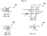
- FIG. 5 A 1 is a diagram 500 A 1 of an exemplary prior art implementation of a two by two switch
- FIG. 5 A 2 is a diagram 500 A 2 for programmable integrated circuit prior art implementation of the diagram 500 A 1 of FIG. 5 A 1
- FIG. 5 A 3 is a diagram 500 A 3 for one-time programmable integrated circuit prior art implementation of the diagram 500 A 1 of FIG. 5 A 1
- FIG. 5 A 4 is a diagram 500 A 4 for integrated circuit placement and route implementation of the diagram 500 A 1 of FIG. 5 A 1 .
- the present invention is concerned with the VLSI layouts of arbitrarily large switching networks for broadcast, unicast and multicast connections.
- Efficient VLSI layout of networks on a semiconductor chip are very important and greatly influence many important design parameters such as the area taken up by the network on the chip, total number of wires, length of the wires, latency of the signals, capacitance and hence the maximum clock speed of operation.
- Some networks may not even be implemented practically on a chip due to the lack of efficient layouts.
- the different varieties of multi-stage networks described above have not been implemented previously on the semiconductor chips efficiently. For example in Field Programmable Gate Array (FPGA) designs, multi-stage networks described in the current invention have not been successfully implemented primarily due to the lack of efficient VLSI layouts.
- FPGA Field Programmable Gate Array
- the current invention discloses the VLSI layouts of numerous types of multi-stage networks which are very efficient. Moreover they can be embedded on to mesh and segmented mesh routing interconnects of current commercial FPGA products.
- the VLSI layouts disclosed in the current invention are applicable to including the numerous generalized multi-stage networks disclosed in the following patent applications, filed concurrently:
- middle stage 130 consists of sixteen, four by four switches MS( 1 , 1 )-MS( 1 , 16 ), middle stage 140 consists of sixteen, four by four switches MS( 2 , 1 )-MS( 2 , 16 ), middle stage 150 consists of sixteen, four by four switches MS( 3 , 1 )-MS( 3 , 16 ), middle stage 160 consists of sixteen, four by four switches MS( 4 , 1 )-MS( 4 , 16 ), middle stage 170 consists of sixteen, four by four switches MS( 5 , 1 )-MS( 5 , 16 ), middle stage 180 consists of sixteen, four by four switches MS( 6 , 1 )-MS( 6 , 16 ), and middle stage 190 consists of sixteen, four by four switches MS( 7 , 1 )-MS( 7 , 16 ).
- such a network can be operated in rearrangeably non-blocking manner for arbitrary fan-out multicast connections and also can be operated in strictly non-blocking manner for unicast connections.
- each of the input switches IS 1 -IS 4 and output switches OS 1 -OS 4 are crossbar switches.
- the number of switches of input stage 110 and of output stage 120 can be denoted in general with the variable N/d, where N is the total number of inlet links or outlet links.
- the number of middle switches in each middle stage is denoted by N/d.
- the size of each input switch IS 1 -IS 4 can be denoted in general with the notation d*2d and each output switch OS 1 -OS 4 can be denoted in general with the notation 2d*d.
- the size of each switch in any of the middle stages can be denoted as 2d*2d.
- a switch as used herein can be either a crossbar switch, or a network of switches each of which in turn may be a crossbar switch or a network of switches.
- a symmetric multi-stage network can be represented with the notation V mlink (N, d, s), where N represents the total number of inlet links of all input switches (for example the links IL 1 -IL 32 ), d represents the inlet links of each input switch or outlet links of each output switch, and s is the ratio of number of outgoing links from each input switch to the inlet links of each input switch.
- Each of the N/d input switches IS 1 -IS 16 are connected to exactly d switches in middle stage 130 through two links each for a total of 2 ⁇ d links (for example input switch IS 1 is connected to middle switch MS( 1 , 1 ) through the links ML( 1 , 1 ), ML( 1 , 2 ), and also connected to middle switch MS( 1 , 2 ) through the links ML( 1 , 3 ) and ML( 1 , 4 )).
- the middle links which connect switches in the same row in two successive middle stages are called hereinafter straight middle links; and the middle links which connect switches in different rows in two successive middle stages are called hereinafter cross middle links.
- middle links ML( 1 , 1 ) and ML( 1 , 2 ) connect input switch IS 1 and middle switch MS( 1 , 1 ), so middle links ML( 1 , 1 ) and ML( 1 , 2 ) are straight middle links; where as the middle links ML( 1 , 3 ) and ML( 1 , 4 ) connect input switch IS 1 and middle switch MS( 1 , 2 ), since input switch IS 1 and middle switch MS( 1 , 2 ) belong to two different rows in diagram 100 A of FIG. 1A , middle links ML( 1 , 3 ) and ML( 1 , 4 ) are cross middle links
- Each of the N/d middle switches MS( 1 , 1 )-MS( 1 , 16 ) in the middle stage 130 are connected from exactly d input switches through two links each for a total of 2 ⁇ d links (for example the links ML( 1 , 1 ) and ML( 1 , 2 ) are connected to the middle switch MS( 1 , 1 ) from input switch IS 1 , and the links ML( 1 , 7 ) and ML( 1 , 8 ) are connected to the middle switch MS( 1 , 1 ) from input switch IS 2 ) and also are connected to exactly d switches in middle stage 140 through two links each for a total of 2 ⁇ d links (for example the links ML( 2 , 1 ) and ML( 2 , 2 ) are connected from middle switch MS( 1 , 1 ) to middle switch MS( 2 , 1 ), and the links ML( 2 , 3 ) and ML( 2 , 4 ) are connected from middle switch MS( 1 , 1 ) to middle switch MS( 2
- Each of the N/d middle switches MS( 2 , 1 )-MS( 2 , 16 ) in the middle stage 140 are connected from exactly d input switches through two links each for a total of 2 ⁇ d links (for example the links ML( 2 , 1 ) and ML( 2 , 2 ) are connected to the middle switch MS( 2 , 1 ) from input switch MS( 1 , 1 ), and the links ML( 1 , 11 ) and ML( 1 , 12 ) are connected to the middle switch MS( 2 , 1 ) from input switch MS( 1 , 3 )) and also are connected to exactly d switches in middle stage 150 through two links each for a total of 2 ⁇ d links (for example the links ML( 3 , 1 ) and ML( 3 , 2 ) are connected from middle switch MS( 2 , 1 ) to middle switch MS( 3 , 1 ), and the links ML( 3 , 3 ) and ML( 3 , 4 ) are connected from middle switch MS( 2 ,
- Each of the N/d middle switches MS( 3 , 1 )-MS( 3 , 16 ) in the middle stage 150 are connected from exactly d input switches through two links each for a total of 2 ⁇ d links (for example the links ML( 3 , 1 ) and ML( 3 , 2 ) are connected to the middle switch MS( 3 , 1 ) from input switch MS( 2 , 1 ), and the links ML( 2 , 19 ) and ML( 2 , 20 ) are connected to the middle switch MS( 3 , 1 ) from input switch MS( 2 , 5 )) and also are connected to exactly d switches in middle stage 160 through two links each for a total of 2 ⁇ d links (for example the links ML( 4 , 1 ) and ML( 4 , 2 ) are connected from middle switch MS( 3 , 1 ) to middle switch MS( 4 , 1 ), and the links ML( 4 , 3 ) and ML( 4 , 4 ) are connected from middle switch MS( 3 ,
- Each of the N/d middle switches MS( 4 , 1 )-MS( 4 , 16 ) in the middle stage 160 are connected from exactly d input switches through two links each for a total of 2 ⁇ d links (for example the links ML( 4 , 1 ) and ML( 4 , 2 ) are connected to the middle switch MS( 4 , 1 ) from input switch MS( 3 , 1 ), and the links ML( 4 , 35 ) and ML( 4 , 36 ) are connected to the middle switch MS( 4 , 1 ) from input switch MS( 3 , 9 )) and also are connected to exactly d switches in middle stage 170 through two links each for a total of 2 ⁇ d links (for example the links ML( 5 , 1 ) and ML( 5 , 2 ) are connected from middle switch MS( 4 , 1 ) to middle switch MS( 5 , 1 ), and the links ML( 5 , 3 ) and ML( 5 , 4 ) are connected from middle switch MS( 4
- Each of the N/d middle switches MS( 5 , 1 )-MS( 5 , 16 ) in the middle stage 170 are connected from exactly d input switches through two links each for a total of 2 ⁇ d links (for example the links ML( 5 , 1 ) and ML( 5 , 2 ) are connected to the middle switch MS( 5 , 1 ) from input switch MS( 4 , 1 ), and the links ML( 5 , 35 ) and ML( 5 , 36 ) are connected to the middle switch MS( 5 , 1 ) from input switch MS( 4 , 9 )) and also are connected to exactly d switches in middle stage 180 through two links each for a total of 2 ⁇ d links (for example the links ML( 6 , 1 ) and ML( 6 , 2 ) are connected from middle switch MS( 5 , 1 ) to middle switch MS( 6 , 1 ), and the links ML( 6 , 3 ) and ML( 6 , 4 ) are connected from middle switch MS( 5
- Each of the N/d middle switches MS( 6 , 1 )-MS( 6 , 16 ) in the middle stage 180 are connected from exactly d input switches through two links each for a total of 2 ⁇ d links (for example the links ML( 6 , 1 ) and ML( 6 , 2 ) are connected to the middle switch MS( 6 , 1 ) from input switch MS( 5 , 1 ), and the links ML( 6 , 19 ) and ML( 6 , 20 ) are connected to the middle switch MS( 6 , 1 ) from input switch MS( 5 , 5 )) and also are connected to exactly d switches in middle stage 190 through two links each for a total of 2 ⁇ d links (for example the links ML( 7 , 1 ) and ML( 7 , 2 ) are connected from middle switch MS( 6 , 1 ) to middle switch MS( 7 , 1 ), and the links ML( 7 , 3 ) and ML( 7 , 4 ) are connected from middle switch MS( 6
- Each of the N/d middle switches MS( 7 , 1 )-MS( 7 , 16 ) in the middle stage 190 are connected from exactly d input switches through two links each for a total of 2 ⁇ d links (for example the links ML( 7 , 1 ) and ML( 7 , 2 ) are connected to the middle switch MS( 7 , 1 ) from input switch MS( 6 , 1 ), and the links ML( 7 , 11 ) and ML( 7 , 12 ) are connected to the middle switch MS( 7 , 1 ) from input switch MS( 6 , 3 )) and also are connected to exactly d switches in middle stage 120 through two links each for a total of 2 ⁇ d links (for example the links ML( 8 , 1 ) and ML( 8 , 2 ) are connected from middle switch MS( 7 , 1 ) to middle switch MS( 8 , 1 ), and the links ML( 8 , 3 ) and ML( 8 , 4 ) are connected from middle switch MS( 7
- Each of the N/d middle switches OS 1 -OS 16 in the middle stage 120 are connected from exactly d input switches through two links each for a total of 2 ⁇ d links (for example the links ML( 8 , 1 ) and ML( 8 , 2 ) are connected to the output switch OS 1 from input switch MS( 7 , 1 ), and the links ML( 8 , 7 ) and ML( 7 , 8 ) are connected to the output switch OS 1 from input switch MS( 7 , 2 )).
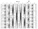
- connection topology of the network 100 A shown in FIG. 1A is known to be back to back inverse Benes connection topology.
- FIG. 1B is a folded version of the multi-link multi-stage network 100 A shown in FIG. 1A .
- the network 100 B in FIG. 1B shows input stage 110 and output stage 120 are placed together. That is input switch IS 1 and output switch OS 1 are placed together, input switch IS 2 and output switch OS 2 are placed together, and similarly input switch IS 16 and output switch OS 16 are placed together.
- forward connecting links ⁇ i.e., inlet links IL 1 -IL 32 and middle links ML( 1 , 1 )-ML( 1 , 64 ) ⁇ correspond to input switches IS 1 -IS 16
- backward connecting links ⁇ i.e., middle links ML( 8 , 1 )-ML( 8 , 64 ) and outlet links OL 1 -OL 32 ⁇ correspond to output switches OS 1 -OS 16 .
- Middle stage 130 and middle stage 190 are placed together. That is middle switches MS( 1 , 1 ) and MS( 7 , 1 ) are placed together, middle switches MS( 1 , 2 ) and MS( 7 , 2 ) are placed together, and similarly middle switches MS( 1 , 16 ) and MS( 7 , 16 ) are placed together.
- All the right going middle links ⁇ i.e., middle links ML( 1 , 1 )-ML( 1 , 64 ) and middle links ML( 2 , 1 )-ML( 2 , 64 ) ⁇ correspond to middle switches MS( 1 , 1 )-MS( 1 , 16 ), and all the left going middle links ⁇ i.e., middle links ML( 7 , 1 )-ML( 7 , 64 ) and middle links ML( 8 , 1 ) and ML( 8 , 64 ) ⁇ correspond to middle switches MS( 7 , 1 )-MS( 7 , 16 ).
- Middle stage 140 and middle stage 180 are placed together. That is middle switches MS( 2 , 1 ) and MS( 6 , 1 ) are placed together, middle switches MS( 2 , 2 ) and MS( 6 , 2 ) are placed together, and similarly middle switches MS( 2 , 16 ) and MS( 6 , 16 ) are placed together.
- All the right going middle links ⁇ i.e., middle links ML( 2 , 1 )-ML( 2 , 64 ) and middle links ML( 3 , 1 )-ML( 3 , 64 ) ⁇ correspond to middle switches MS( 2 , 1 )-MS( 2 , 16 ), and all the left going middle links ⁇ i.e., middle links ML( 6 , 1 )-ML( 6 , 64 ) and middle links ML( 7 , 1 ) and ML( 7 , 64 ) ⁇ correspond to middle switches MS( 6 , 1 )-MS( 6 , 16 ).
- Middle stage 150 and middle stage 170 are placed together. That is middle switches MS( 3 , 1 ) and MS( 5 , 1 ) are placed together, middle switches MS( 3 , 2 ) and MS( 5 , 2 ) are placed together, and similarly middle switches MS( 3 , 16 ) and MS( 5 , 16 ) are placed together.
- All the right going middle links ⁇ i.e., middle links ML( 3 , 1 )-ML( 3 , 64 ) and middle links ML( 4 , 1 )-ML( 4 , 64 ) ⁇ correspond to middle switches MS( 3 , 1 )-MS( 3 , 16 ), and all the left going middle links ⁇ i.e., middle links ML( 5 , 1 )-ML( 5 , 64 ) and middle links ML( 6 , 1 ) and ML( 6 , 64 ) ⁇ correspond to middle switches MS( 5 , 1 )-MS( 5 , 16 ).
- Middle stage 160 is placed alone. All the right going middle links are the middle links ML( 4 , 1 )-ML( 4 , 64 ) and all the left going middle links are middle links ML( 5 , 1 )-ML( 5 , 64 ).
- the switch input switch IS 1 and output switch OS 1 are placed together; so input switch IS 1 is implemented as two by four switch with the inlet links IL 1 and IL 2 being the inputs of the input switch IS 1 and middle links ML( 1 , 1 )-ML( 1 , 4 ) being the outputs of the input switch IS 1 ; and output switch OS 1 is implemented as four by two switch with the middle links ML( 8 , 1 ), ML( 8 , 2 ), ML( 8 , 7 ) and ML( 8 , 8 ) being the inputs of the output switch OS 1 and outlet links OL 1 -OL 2 being the outputs of the output switch OS 1 .
- all the switches that are placed together in each middle stage are implemented as separate switches.
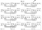
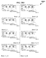
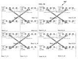
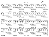
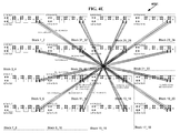
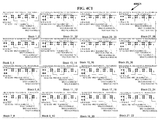
- Block 1 _ 2 there are sixteen blocks namely Block 1 _ 2 , Block 3 _ 4 , Block 5 _ 6 , Block 7 _ 8 , Block 9 _ 10 , Block 11 _ 12 , Block 13 _ 14 , Block 15 _ 16 , Block 17 _ 18 , Block 19 _ 20 , Block 21 _ 22 , Block 23 _ 24 , Block 25 _ 26 , Block 27 _ 28 , Block 29 _ 30 , and Block 31 _ 32 .
- Each block implements all the switches in one row of the network 100 B of FIG. 1B , one of the key aspects of the current invention.
- Block 1 _ 2 implements the input switch IS 1 , output Switch OS 1 , middle switch MS( 1 , 1 ), middle switch MS( 7 , 1 ), middle switch MS( 2 , 1 ), middle switch MS( 6 , 1 ), middle switch MS( 3 , 1 ), middle switch MS( 5 , 1 ), and middle switch MS( 4 , 1 ).
- Input switch IS 1 and output switch OS 1 together are denoted as switch 1 ;
- Middle switch MS( 1 , 1 ) and middle switch MS( 7 , 1 ) together are denoted by switch 2 ;
- Middle switch MS( 2 , 1 ) and middle switch MS( 6 , 1 ) together are denoted by switch 3 ;
- Middle switch MS( 3 , 1 ) and middle switch MS( 5 , 1 ) together are denoted by switch 4 ;
- Middle switch MS( 4 , 1 ) is denoted by switch 5 .
- inlet links IL 1 -IL 2 , outlet links OL 1 -OL 2 , middle link ML( 1 , 1 ), middle link ML( 1 , 2 ), middle link ML( 8 , 1 ), middle link ML( 8 , 2 ), middle link ML( 2 , 1 ), middle link ML( 2 , 2 ), middle link ML( 7 , 1 ), middle link ML( 7 , 2 ), middle link ML( 3 , 1 ), middle link ML( 3 , 2 ), middle link ML( 6 , 1 ), middle link ML( 6 , 2 ), middle link ML( 4 , 1 ), middle link ML( 4 , 2 ), middle link ML( 5 , 1 ) and middle link ML( 5 , 2 ) are illustrated in layout 100 C of FIG. 1C .
- each block in addition to the switches there may be Configurable Logic Blocks (CLB) or any arbitrary digital circuit (hereinafter “sub-integrated circuit block”) depending on the applications in different embodiments.
- CLB Configurable Logic Blocks
- sub-integrated circuit block any arbitrary digital circuit
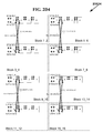
- Top-left quadrant implements Block 1 _ 2 , Block 3 _ 4 , Block 5 _ 6 , and Block 7 _ 8 .
- Bottom-left quadrant implements Block 9 _ 10 , Block 11 _ 12 , Block 13 _ 14 , and Block 15 _ 16 .
- Top-right quadrant implements Block 17 _ 18 , Block 19 _ 20 , Block 21 _ 22 , and Block 23 _ 24 .
- Bottom-right quadrant implements Block 25 _ 26 , Block 27 _ 28 , Block 29 _ 30 , and Block 31 _ 32 .
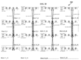
- each quadrant there are four sub-quadrants.
- there are four sub-quadrants namely top-left sub-quadrant, bottom-left sub-quadrant, top-right sub-quadrant and bottom-right sub-quadrant.
- Top-left sub-quadrant of top-left quadrant implements Block 1 _ 2 .
- Bottom-left sub-quadrant of top-left quadrant implements Block 3 _ 4 .
- Top-right sub-quadrant of top-left quadrant implements Block 5 _ 6 .
- Finally bottom-right sub-quadrant of top-left quadrant implements Block 7 _ 8 .
- top-left quadrant there are two sub-halves namely left-sub-half and right-sub-half.
- Left-sub-half of top-left quadrant implements Block 1 _ 2 and Block 3 _ 4 .
- Right-sub-half of top-left quadrant implements Block 5 _ 6 and Block 7 _ 8
- the layout in this embodiment in accordance with the current invention will be such that the super-quadrants will also be arranged in d-ary hypercube manner.
- it is binary hypercube manner since d 2, in the network V fold-mlink (N 1 , N 2 , d, s) 100 B of FIG. 1B ).
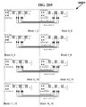
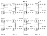
- Layout 100 D of FIG. 1D illustrates the inter-block links between switches 1 and 2 of each block.
- middle links ML( 1 , 3 ), ML( 1 , 4 ), ML( 8 , 7 ), and ML( 8 , 8 ) are connected between switch 1 of Block 1 _ 2 and switch 2 of Block 3 _ 4 .
- middle links ML( 1 , 7 ), ML( 1 , 8 ), ML( 8 , 3 ), and ML( 8 , 4 ) are connected between switch 2 of Block 1 _ 2 and switch 1 of Block 3 _ 4 .
- the inter-block links illustrated in layout 100 D of FIG. 1D can be implemented as vertical tracks in one embodiment.
- inter-block links are implemented as two different tracks (for example middle links ML( 1 , 4 ) and ML( 8 , 8 ) are implemented as two different tracks); or in an alternative embodiment inter-block links are implemented as a time division multiplexed single track (for example middle links ML( 1 , 4 ) and ML( 8 , 8 ) are implemented as a time division multiplexed single track).
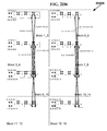
- Layout 100 E of FIG. 1E illustrates the inter-block links between switches 2 and 3 of each block.
- middle links ML( 2 , 3 ), ML( 2 , 4 ), ML( 7 , 11 ), and ML( 7 , 12 ) are connected between switch 2 of Block 1 _ 2 and switch 3 of Block 3 _ 4 .
- middle links ML( 2 , 11 ), ML( 2 , 12 ), ML( 7 , 3 ), and ML( 7 , 4 ) are connected between switch 3 of Block 1 _ 2 and switch 2 of Block 3 _ 4 .
- the inter-block links illustrated in layout 100 E of FIG. 1E can be implemented as horizontal tracks in one embodiment.
- inter-block links are implemented as two different tracks (for example middle links ML( 2 , 12 ) and ML( 7 , 4 ) are implemented as two different tracks); or in an alternative embodiment inter-block links are implemented as a time division multiplexed single track (for example middle links ML( 2 , 12 ) and ML( 7 , 4 ) are implemented as a time division multiplexed single track).
- Layout 100 F of FIG. 1F illustrates the inter-block links between switches 3 and 4 of each block.
- middle links ML( 3 , 3 ), ML( 3 , 4 ), ML( 6 , 19 ), and ML( 6 , 20 ) are connected between switch 3 of Block 1 _ 2 and switch 4 of Block 3 _ 4 .
- middle links ML( 3 , 19 ), ML( 3 , 20 ), ML( 6 , 3 ), and ML( 6 , 4 ) are connected between switch 4 of Block 1 _ 2 and switch 3 of Block 3 _ 4 .
- the inter-block links illustrated in layout 100 F of FIG. 1F can be implemented as vertical tracks in one embodiment.
- inter-block links are implemented as two different tracks (for example middle links ML( 3 , 4 ) and ML( 6 , 20 ) are implemented as two different tracks); or in an alternative embodiment inter-block links are implemented as a time division multiplexed single track (for example middle links ML( 3 , 4 ) and ML( 6 , 20 ) are implemented as a time division multiplexed single track).
- Layout 100 G of FIG. 1G illustrates the inter-block links between switches 4 and 5 of each block.
- middle links ML( 4 , 3 ), ML( 4 , 4 ), ML( 5 , 35 ), and ML( 5 , 36 ) are connected between switch 4 of Block 1 _ 2 and switch 5 of Block 3 _ 4 .
- middle links ML( 4 , 35 ), ML( 4 , 36 ), ML( 5 , 3 ), and ML( 5 , 4 ) are connected between switch 5 of Block 1 _ 2 and switch 4 of Block 3 _ 4 .
- the inter-block links illustrated in layout 100 G of FIG. 1G can be implemented as horizontal tracks in one embodiment.
- inter-block links are implemented as two different tracks (for example middle links ML( 4 , 4 ) and ML( 5 , 36 ) are implemented as two different tracks); or in an alternative embodiment inter-block links are implemented as a time division multiplexed single track (for example middle links ML( 4 , 4 ) and ML( 5 , 36 ) are implemented as a time division multiplexed single track).
- the complete layout for the network 100 B of FIG. 1B is given by combining the links in layout diagrams of 100 C, 100 D, 100 E, 100 F, and 100 G.
- the inter-block links between switch 1 and switch 2 of corresponding blocks are vertical tracks as shown in layout 100 D of FIG. 1D ;
- the inter-block links between switch 2 and switch 3 of corresponding blocks are horizontal tracks as shown in layout 100 E of FIG. 1E ;
- the inter-block links between switch 3 and switch 4 of corresponding blocks are vertical tracks as shown in layout 100 F of FIG. 1F ;
- the inter-block links between switch 4 and switch 5 of corresponding blocks are horizontal tracks as shown in layout 100 G of FIG. 1G .
- the pattern is alternate vertical tracks and horizontal tracks. It continues recursively for larger networks of N>32 as will be illustrated later.
- All the switches in one row of the multi-stage network 100 B are implemented in a single block. 2) The blocks are placed in such a way that all the inter-block links are either horizontal tracks or vertical tracks; 3) Since all the inter-block links are either horizontal or vertical tracks, all the inter-block links can be mapped on to island-style architectures in current commercial FPGA's; 4) The length of the longest wire is about half of the width (or length) of the complete layout (For example middle link ML( 4 , 4 ) is about half the width of the complete layout).
- the layout 100 C in FIG. 1C can be recursively extended for any arbitrarily large generalized folded multi-link multi-stage network V fold-mlink (N 1 , N 2 , d, s) the sub-quadrants, quadrants, and super-quadrants are arranged in d-ary hypercube manner and also the inter-blocks are accordingly connected in d-ary hypercube topology.
- N 1 N 2
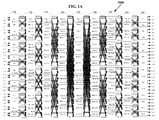
- d the layout 100 H of FIG.
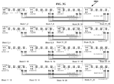
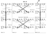
- There are four super-quadrants in layout 100 H namely top-left super-quadrant, bottom-left super-quadrant, top-right super-quadrant, bottom-right super-quadrant.
- Total number of blocks in the layout 100 H is sixty four.
- Top-left super-quadrant implements the blocks from block 1 _ 2 to block 31 _ 32 .
- Each block in all the super-quadrants has two more switches namely switch 6 and switch 7 in addition to the switches [ 1 - 5 ] illustrated in layout 100 C of FIG. 1C .
- the inter-block link connection topology is the exactly the same between the switches 1 and 2 ; switches 2 and 3 ; switches 3 and 4 ; switches 4 and 5 as it is shown in the layouts of FIG. 1D , FIG. 1E , FIG. 1F , and FIG. 1G respectively.
- Bottom-left super-quadrant implements the blocks from block 33 _ 34 to block 63 _ 64 .
- Top-right super-quadrant implements the blocks from block 65 _ 66 to block 95 _ 96 .
- bottom-right super-quadrant implements the blocks from block 97 _ 98 to block 127 _ 128 .
- the inter-block link connection topology is the exactly the same between the switches 1 and 2 ; switches 2 and 3 ; switches 3 and 4 ; switches 4 and 5 as that of the top-left super-quadrant.
- the inter-block links connecting the switch 5 and switch 6 will be vertical tracks between the corresponding switches of top-left super-quadrant and bottom-left super-quadrant. And similarly the inter-block links connecting the switch 5 and switch 6 will be vertical tracks between the corresponding switches of top-right super-quadrant and bottom-right super-quadrant.
- the inter-block links connecting the switch 6 and switch 7 will be horizontal tracks between the corresponding switches of top-left super-quadrant and top-right super-quadrant. And similarly the inter-block links connecting the switch 6 and switch 7 will be horizontal tracks between the corresponding switches of bottom-left super-quadrant and bottom-right super-quadrant.
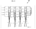
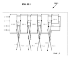
- switches that are placed together in Block 1 _ 2 as shown in FIG. 1I are namely input switch IS 1 and output switch OS 1 belonging to switch 1 , illustrated by dotted lines, (as noted before switch 1 is for illustration purposes only, in practice the switches implemented are input switch IS 1 and output switch OS 1 ); middle switch MS( 1 , 1 ) and middle switch MS( 7 , 1 ) belonging to switch 2 ; middle switch MS( 2 , 1 ) and middle switch MS( 6 , 1 ) belonging to switch 3 ; middle switch MS( 3 , 1 ) and middle switch MS( 5 , 1 ) belonging to switch 4 ; And middle switch MS( 4 , 1 ) belonging to switch 5 .
- Input switch IS 1 is implemented as two by four switch with the inlet links IL 1 and IL 2 being the inputs of the input switch IS 1 and middle links ML( 1 , 1 )-ML( 1 , 4 ) being the outputs of the input switch IS 1 ; and output switch OS 1 is implemented as four by two switch with the middle links ML( 8 , 1 )-ML( 8 , 4 ) being the inputs of the output switch OS 1 and outlet links OL 1 -OL 2 being the outputs of the output switch OS 1 .
- Middle switch MS( 1 , 1 ) is implemented as four by four switch with the middle links ML( 1 , 1 ), ML( 1 , 2 ), ML( 1 , 7 ) and ML( 1 , 8 ) being the inputs and middle links ML( 2 , 1 )-ML( 2 , 4 ) being the outputs; and middle switch MS( 7 , 1 ) is implemented as four by four switch with the middle links ML( 7 , 1 ), ML( 7 , 2 ), ML( 7 , 11 ) and ML( 7 , 12 ) being the inputs and middle links ML( 8 , 1 )-ML( 8 , 4 ) being the outputs.
- all the other middle switches are also implemented as four by four switches as illustrated in 100 I of FIG. 1I .
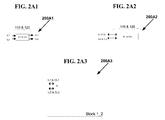
- Layout 200 A 3 of FIG. 2 A 3 illustrates the VLSI layout of the network 200 A 2 of FIG. 2 A 2 .
- Block 1 _ 2 comprising switch 1 .
- switch 1 consists of input switch IS 1 and output switch OS 1 .
- Layout 200 B 3 of FIG. 2 B 3 illustrates the VLSI layout of the network 200 B 2 of FIG. 2 B 2 .
- Block 1 _ 2 and Block 3 _ 4 each comprising switch 1 and switch 2 .
- Switch 1 in each block consists of the corresponding input switch and output switch.
- switch 1 in Block 1 _ 2 consists of input switch IS 1 and output switch OS 1 .
- switch 2 in Block 1 _ 2 consists of middle switch ( 1 , 1 ).
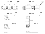
- Layout 200 B 4 of FIG. 2 B 4 illustrates the inter-block links of the VLSI layout diagram 200 B 3 of FIG. 2 B 3 .
- all the inter-block links are vertical tracks in this layout. (Alternatively all the inter-blocks can also be implemented as horizontal tracks).
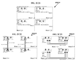
- Layout 200 C 21 of FIG. 2 C 21 illustrates the VLSI layout of the network 200 C 12 of FIG. 2 C 12 .
- Block 1 _ 2 There are four blocks i.e., Block 1 _ 2 , Block 3 _ 4 , Block 5 _ 6 , and Block 7 _ 8 each comprising switch 1 , switch 2 and switch 3 .
- switch 1 in Block 1 _ 2 consists of input switch IS 1 and output switch OS 1 ;
- Switch 2 in Block 1 _ 2 consists of MS( 1 , 1 ) and MS( 3 , 1 ).
- Switch 3 in Block 1 _ 2 consists of MS( 2 , 1 ).
- Layout 200 C 22 of FIG. 2 C 22 illustrates the inter-block links between the switch 1 and switch 2 of the VLSI layout diagram 200 C 21 of FIG. 2 C 21 .
- middle links ML( 1 , 4 ) and ML( 4 , 8 ) are connected between Block 1 _ 2 and Block 3 _ 4 .
- all the inter-block links between switch 1 and switch 2 of all blocks are vertical tracks in this layout.
- Layout 200 C 23 of FIG. 2 C 23 illustrates the inter-block links between the switch 2 and switch 3 of the VLSI layout diagram 200 C 21 of FIG. 2 C 21 .
- middle links ML( 2 , 12 ) and ML( 3 , 4 ) are connected between Block 1 _ 2 and Block 5 _ 6 .
- all the inter-block links between switch 2 and switch 3 of all blocks are horizontal tracks in this layout
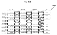
- Layout 200 D 3 of FIG. 2 D 3 illustrates the VLSI layout of the network 200 D 2 of FIG. 2 D 2 .
- Block 1 _ 2 There are eight blocks i.e., Block 1 _ 2 , Block 3 _ 4 , Block 5 _ 6 , Block 7 _ 8 , Block 9 _ 10 , Block 11 _ 12 , Block 13 _ 14 and Block 15 _ 16 each comprising switch 1 , switch 2 , switch 3 and switch 4 .
- switch 1 in Block 1 _ 2 consists of input switch IS 1 and output switch OS 1 ;
- Switch 2 in Block 1 _ 2 consists of MS( 1 , 1 ) and MS( 5 , 1 ).
- Switch 3 in Block 1 _ 2 consists of MS( 2 , 1 ) and MS( 4 , 1 ), and switch 4 in Block 1 _ 2 consists of MS( 3 , 1 ).
- Layout 200 D 4 of FIG. 2 D 4 illustrates the inter-block links between the switch 1 and switch 2 of the VLSI layout diagram 200 D 3 of FIG. 2 D 3 .
- middle links ML( 1 , 4 ) and ML( 6 , 8 ) are connected between Block 1 _ 2 and Block 3 _ 4 .
- all the inter-block links between switch 1 and switch 2 of all blocks are vertical tracks in this layout.
- Layout 200 D 5 of FIG. 2 D 5 illustrates the inter-block links between the switch 2 and switch 3 of the VLSI layout diagram 200 D 3 of FIG. 2 D 3 .
- middle links ML( 2 , 12 ) and ML( 5 , 4 ) are connected between Block 1 _ 2 and Block 5 _ 6 .
- Layout 200 D 6 of FIG. 2 D 6 illustrates the inter-block links between the switch 3 and switch 4 of the VLSI layout diagram 200 D 3 of FIG. 2 D 3 .
- middle links ML( 3 , 4 ) and ML( 4 , 20 ) are connected between Block 1 _ 2 and Block 9 _ 10 .
- all the inter-block links between switch 3 and switch 4 of all blocks are vertical tracks in this layout.
- input switch IS 1 and output switch OS 1 are placed together; so input switch IS 1 and output OS 1 are implemented as a six by six switch with the inlet links IL 1 , IL 2 , ML( 8 , 1 ), ML( 8 , 2 ), ML( 8 , 7 ) and ML( 8 , 8 ) being the inputs of the combined switch (denoted as IS 1 &OS 1 ) and middle links ML( 1 , 1 ), ML( 1 , 2 ), ML( 1 , 3 ), ML( 1 , 4 ), OL 1 and OL 2 being the outputs of the combined switch IS 1 &OS 1 .
- all the switches that are placed together are implemented as a combined switch.
- the layout 100 C in FIG. 1C can be recursively extended for any arbitrarily large generalized multi-link butterfly fat tree network V mlink-bft (N 1 , N 2 , d, s).
- layout 100 H of FIG. 1H is also applicable to generalized multi-link butterfly fat tree network V mlink-bft (N 1 , N 2 , d, s).
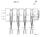
- Block 1 _ 2 in 100 J illustrates both the intra-block and inter-block links.
- the layout diagram 100 J corresponds to the embodiment where the switches that are placed together are implemented as combined switch in the network 100 B of FIG. 1B .
- switches that are placed together in Block 1 _ 2 as shown in FIG. 1J are namely the combined input and output switch IS 1 &OS 1 belonging to switch 1 , illustrated by dotted lines, (as noted before switch 1 is for illustration purposes only, in practice the switch implemented is combined input and output switch IS 1 &OS 1 ); middle switch MS( 1 , 1 ) belonging to switch 2 ; middle switch MS( 2 , 1 ) belonging to switch 3 ; middle switch MS( 3 , 1 ) belonging to switch 4 ; And middle switch MS( 4 , 1 ) belonging to switch 5 .
- Combined input and output switch IS 1 &OS 1 is implemented as six by six switch with the inlet links IL 1 , IL 2 and ML( 8 , 1 )-ML( 8 , 4 ) being the inputs and middle links ML( 1 , 1 )-ML( 1 , 4 ), and outlet links OL 1 -OL 2 being the outputs.
- middle switch MS( 1 , 1 ) any one of the right going middle links can be switched to any one of the left going middle links and hereinafter middle switch MS( 1 , 1 ) provides U-turn links.
- middle switch MS( 1 , 1 ) provides U-turn links.
- V mlink-bft (N 1 , N 2 , d, s) each input switch, each output switch and each middle switch provides U-turn links.
- middle switch MS( 1 , 1 ) (or the middle switches in any of the middle stage excepting the root middle stage) of Block 1 _ 2 of V mlink-bft (N 1 , N 2 , d, s) can be implemented as a four by eight switch and a four by four switch to save cross points. This is because the left going middle links of these middle switches are never setup to the right going middle links For example, in middle switch MS( 1 , 1 ) of Block 1 _ 2 as shown FIG.
- the left going middle links namely ML( 7 , 1 ), ML( 7 , 2 ), ML( 7 , 11 ), and ML( 7 , 12 ) are never switched to the right going middle links ML( 2 , 1 ), ML( 2 , 2 ), ML( 2 , 3 ), and ML( 2 , 4 ).
- MS( 1 , 1 ) two switches namely: 1) a four by eight switch with the middle links ML( 1 , 1 ), ML( 1 , 2 ), ML( 1 , 7 ), and ML( 1 , 8 ) as inputs and the middle links ML( 2 , 1 ), ML( 2 , 2 ), ML( 2 , 3 ), ML( 2 , 4 ), ML( 8 , 1 ), ML( 8 , 2 ), ML( 8 , 3 ), and ML( 8 , 4 ) as outputs and 2) a four by four switch with the middle links ML( 7 , 1 ), ML( 7 , 2 ), ML( 7 , 11 ), and ML( 7 , 12 ) as inputs and the middle links ML( 8 , 1 ), ML( 8 , 2 ), ML( 8 , 3 ), and ML( 8 , 4 ) as outputs are sufficient without loosing any connectivity of the embodiment
- the switches corresponding to the middle stages that are placed together are implemented as four two by two switches.
- middle switches MS( 1 , 1 ), MS( 1 , 17 ), MS( 7 , 1 ), and MS( 7 , 17 ) are placed together; so middle switch MS( 1 , 1 ) is implemented as two by two switch with middle links ML( 1 , 1 ) and ML( 1 , 7 ) being the inputs and middle links ML( 2 , 1 ) and ML( 2 , 3 ) being the outputs;
- middle switch MS( 1 , 17 ) is implemented as two by two switch with the middle links ML( 1 , 2 ) and ML( 1 , 8 ) being the inputs and middle links ML( 2 , 2 ) and ML( 2 , 4 ) being the outputs;
- middle switch MS( 7 , 1 ) is implemented as two by two switch with middle links ML( 7 , 1 ) and ML( 7 , 11 ) being the inputs and middle links
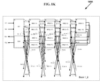
- the layout 100 C in FIG. 1C can be recursively extended for any arbitrarily large generalized folded multi-stage network V fold (N 1 , N 2 , d, s).
- layout 100 H of FIG. 1H is also applicable to generalized folded multi-stage network V fold (N 1 , N 2 , d, s).
- Block 1 _ 2 in 100 K illustrates both the intra-block and inter-block links.
- the layout diagram 100 K corresponds to the embodiment where the switches that are placed together are implemented as separate switches in the network 100 B of FIG. 1B .
- switches that are placed together in Block 1 _ 2 as shown in FIG. 1K are namely the input switch IS 1 and output switch OS 1 belonging to switch 1 , illustrated by dotted lines, (as noted before switch 1 is for illustration purposes only, in practice the switches implemented are input switch IS 1 and output switch OS 1 ); middle switches MS( 1 , 1 ), MS( 1 , 17 ), MS( 7 , 1 ) and MS( 7 , 17 ) belonging to switch 2 ; middle switches MS( 2 , 1 ), MS( 2 , 17 ), MS( 6 , 1 ) and MS( 6 , 17 ) belonging to switch 3 ; middle switches MS( 3 , 1 ), MS( 3 , 17 ), MS( 5 , 1 ) and MS( 5 , 17 ) belonging to switch 4 ; And middle switches MS( 4 , 1 ), and MS( 4 , 17 ) belonging to switch 5 .
- the switches corresponding to the middle stages that are placed together are implemented as two, two by two switches.
- middle switches MS( 1 , 1 ) and MS( 7 , 1 ) are placed together; so middle switch MS( 1 , 1 ) is implemented as two by two switch with middle links ML( 1 , 1 ) and ML( 1 , 3 ) being the inputs and middle links ML( 2 , 1 ) and ML( 2 , 2 ) being the outputs; middle switch MS( 7 , 1 ) is implemented as two by two switch with middle links ML( 7 , 1 ) and ML( 7 , 5 ) being the inputs and middle links ML( 8 , 1 ) and ML( 8 , 2 ) being the outputs; Similarly in this embodiment of network 100 B all the switches that are placed together are implemented as two separate switches.
- the layout 100 C in FIG. 1C can be recursively extended for any arbitrarily large generalized folded multi-stage network V fold (N 1 , N 2 , d, s).
- layout 100 H of FIG. 1H is also applicable to generalized folded multi-stage network V fold (N 1 , N 2 , d, s).
- switches that are placed together in Block 1 _ 2 as shown in FIG. 1 K 1 are namely the input switch IS 1 and output switch OS 1 belonging to switch 1 , illustrated by dotted lines, (as noted before switch 1 is for illustration purposes only, in practice the switches implemented are input switch IS 1 and output switch OS 1 ); middle switches MS( 1 , 1 ) and MS( 7 , 1 ) belonging to switch 2 ; middle switches MS( 2 , 1 ) and MS( 6 , 1 ) belonging to switch 3 ; middle switches MS( 3 , 1 ) and MS( 5 , 1 ) belonging to switch 4 ; And middle switch MS( 4 , 1 ) belonging to switch 5 .
- Input switch IS 1 and output switch OS 1 are placed together; so input switch IS 1 is implemented as two by two switch with the inlet links IL 1 and IL 2 being the inputs and middle links ML( 1 , 1 )-ML( 1 , 2 ) being the outputs; and output switch OS 1 is implemented as two by two switch with the middle links ML( 8 , 1 ) and ML( 8 , 3 ) being the inputs and outlet links OL 1 -OL 2 being the outputs.
- Middle switches MS( 1 , 1 ) and MS( 7 , 1 ) are placed together; so middle switch MS( 1 , 1 ) is implemented as two by two switch with middle links ML( 1 , 1 ) and ML( 1 , 3 ) being the inputs and middle links ML( 2 , 1 ) and ML( 2 , 2 ) being the outputs; And middle switch MS( 7 , 1 ) is implemented as two by two switch with middle links ML( 7 , 1 ) and ML( 7 , 5 ) being the inputs and middle links ML( 8 , 1 ) and ML( 8 , 2 ) being the outputs. Similarly all the other middle switches are also implemented as two by two switches as illustrated in 100 K 1 of FIG. 1 K 1 .
- input switch IS 1 and output switch OS 1 are placed together; so input output switch IS 1 &OS 1 are implemented as a six by six switch with the inlet links IL 1 , IL 2 , ML( 8 , 1 ), ML( 8 , 2 ), ML( 8 , 7 ) and ML( 8 , 8 ) being the inputs of the combined switch (denoted as IS 1 &OS 1 ) and middle links ML( 1 , 1 ), ML( 1 , 2 ), ML( 1 , 3 ), ML( 1 , 4 ), OL 1 and OL 2 being the outputs of the combined switch IS 1 &OS 1 .
- the switches corresponding to the middle stages that are placed together are implemented as two four by four switches.
- middle switches MS( 1 , 1 ) and MS( 1 , 17 ) are placed together; so middle switch MS( 1 , 1 ) is implemented as four by four switch with middle links ML( 1 , 1 ), ML( 1 , 7 ), ML( 7 , 1 ) and ML( 7 , 11 ) being the inputs and middle links ML( 2 , 1 ), ML( 2 , 3 ), ML( 8 , 1 ) and ML( 8 , 3 ) being the outputs; middle switch MS( 1 , 17 ) is implemented as four by four switch with the middle links ML( 1 , 2 ), ML( 1 , 8 ), ML( 7 , 2 ) and ML( 7 , 12 ) being the inputs and middle links ML( 2 , 2 ), ML( 2 , 4 ), ML( 8 , 2 ) and ML( 8 , 4
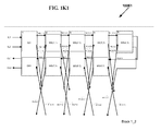
- the layout 100 C in FIG. 1C can be recursively extended for any arbitrarily large generalized butterfly fat tree network V bft (N 1 , N 2 , d, s).
- layout 100 H of FIG. 1H is also applicable to generalized butterfly fat tree network V bft (N 1 , N 2 , d, s).
- Block 1 _ 2 in 100 L illustrates both the intra-block and inter-block links.
- the layout diagram 100 L corresponds to the embodiment where the switches that are placed together are implemented as two combined switches in the network 100 B of FIG. 1B .
- switches that are placed together in Block 1 _ 2 as shown in FIG. 1L are namely the combined input and output switch IS 1 &OS 1 belonging to switch 1 , illustrated by dotted lines, (as noted before switch 1 is for illustration purposes only, in practice the switch implemented is combined input and output switch IS 1 &OS 1 ); middle switch MS( 1 , 1 ) and MS( 1 , 17 ) belonging to switch 2 ; middle switch MS( 2 , 1 ) and MS( 2 , 17 ) belonging to switch 3 ; middle switch MS( 3 , 1 ) and MS( 3 , 17 ) belonging to switch 4 ; And middle switch MS( 4 , 1 ) belonging to switch 5 .
- Combined input and output switch IS 1 &OS 1 is implemented as six by six switch with the inlet links IL 1 , IL 2 , ML( 8 , 1 ), ML( 8 , 2 ), ML( 8 , 7 ) and ML( 8 , 8 ) being the inputs and middle links ML( 1 , 1 )-ML( 1 , 4 ) and outlet links OL 1 -OL 2 being the outputs.
- Middle switch MS( 1 , 1 ) is implemented as four by four switch with middle links ML( 1 , 1 ), ML( 1 , 7 ), ML( 7 , 1 ) and ML( 7 , 11 ) being the inputs and middle links ML( 2 , 1 ), ML( 2 , 3 ), ML( 8 , 1 ) and ML( 8 , 3 ) being the outputs;
- middle switch MS( 1 , 17 ) is implemented as four by four switch with the middle links ML( 1 , 2 ), ML( 1 , 8 ), ML( 7 , 2 ) and ML( 7 , 12 ) being the inputs and middle links ML( 2 , 2 ), ML( 2 , 4 ), ML( 8 , 2 ) and ML( 8 , 4 ) being the outputs.
- middle switch MS( 1 , 1 ) any one of the right going middle links can be switched to any one of the left going middle links and hereinafter middle switch MS( 1 , 1 ) provides U-turn links.
- middle switch MS( 1 , 1 ) provides U-turn links.
- V bft (N 1 , N 2 , d, s) each input switch, each output switch and each middle switch provides U-turn links.
- middle switch MS( 1 , 1 ) (or the middle switches in any of the middle stage excepting the root middle stage) of Block 1 _ 2 of V bft (N 1 , N 2 , d, s) can be implemented as a two by four switch and a two by two switch to save cross points. This is because the left going middle links of these middle switches are never setup to the right going middle links.
- middle switch MS( 1 , 1 ) of Block 1 _ 2 as shown FIG. 1L the left going middle links namely ML( 7 , 1 ) and ML( 7 , 11 ) are never switched to the right going middle links ML( 2 , 1 ) and ML( 2 , 3 ).
- MS( 1 , 1 ) two switches namely: 1) a two by four switch with the middle links ML( 1 , 1 ) and ML( 1 , 7 ) as inputs and the middle links ML( 2 , 1 ), ML( 2 , 3 ), ML( 8 , 1 ), and ML( 8 , 3 ) as outputs and 2) a two by two switch with the middle links ML( 7 , 1 ) and ML( 7 , 11 ) as inputs and the middle links ML( 8 , 1 ) and ML( 8 , 3 ) as outputs are sufficient without loosing any connectivity of the embodiment of MS( 1 , 1 ) being implemented as an eight by eight switch as described before.)
- switch input switch IS 1 and output switch OS 1 are placed together; so input and output switch IS 1 &OS 1 is implemented as four by four switch with the inlet links IL 1 , IL 2 , ML( 8 , 1 ) and ML( 8 , 3 ) being the inputs and middle links ML( 1 , 1 )-ML( 1 , 2 ) and outlet links OL 1 -OL 2 being the outputs
- the switches corresponding to the middle stages that are placed together are implemented as a four by four switch.
- middle switches MS( 1 , 1 ) is implemented as four by four switch with middle links ML( 1 , 1 ), ML( 1 , 3 ), ML( 7 , 1 ) and ML( 7 , 5 ) being the inputs and middle links ML( 2 , 1 ), ML( 2 , 2 ), ML( 8 , 1 ) and ML( 8 , 2 ) being the outputs.
- the layout 100 C in FIG. 1C can be recursively extended for any arbitrarily large generalized butterfly fat tree network V bft (N 1 , N 2 , d, s).
- layout 100 H of FIG. 1H is also applicable to generalized butterfly fat tree network V bft (N 1 , N 2 , d, s).
- Block 1 _ 2 in 100 K 1 illustrates both the intra-block and inter-block links
- switches that are placed together in Block 1 _ 2 as shown in FIG. 1 L 1 are namely the input and output switch IS 1 &OS 1 belonging to switch 1 , illustrated by dotted lines, (as noted before switch 1 is for illustration purposes only, in practice the switches implemented are input switch IS 1 and output switch OS 1 ); middle switch MS( 1 , 1 ) belonging to switch 2 ; middle switch MS( 2 , 1 ) belonging to switch 3 ; middle switch MS( 3 , 1 ) belonging to switch 4 ; And middle switch MS( 4 , 1 ) belonging to switch 5 .
- Input and output switch IS 1 &OS 1 are placed together; so input and output switch IS 1 &OS 1 is implemented as four by four switch with the inlet links IL 1 , IL 2 , ML( 8 , 1 ) and ML( 8 , 3 ) being the inputs and middle links ML( 1 , 1 )-ML( 1 , 2 ) and outlet links OL 1 -OL 2 being the outputs.
- Middle switch MS( 1 , 1 ) is implemented as four by four switch with middle links ML( 1 , 1 ), ML( 1 , 3 ), ML( 7 , 1 ) and ML( 7 , 5 ) being the inputs and middle links ML( 2 , 1 ), ML( 2 , 2 ), ML( 8 , 1 ) and ML( 8 , 2 ) being the outputs.
- all the other middle switches are also implemented as four by four switches as illustrated in 100 L 1 of FIG. 1 L 1 .
- middle switch MS( 1 , 1 ) (or the middle switches in any of the middle stage excepting the root middle stage) of Block 1 _ 2 of V mlink-bft (N 1 , N 2 , d, s) can be implemented as a two by four switch and a two by two switch to save cross points. This is because the left going middle links of these middle switches are never setup to the right going middle links
- middle switch MS( 1 , 1 ) of Block 1 _ 2 as shown FIG. 1 L 1 the left going middle links namely ML( 7 , 1 ) and ML( 7 , 5 ) are never switched to the right going middle links ML( 2 , 1 ) and ML( 2 , 2 ).
- MS( 1 , 1 ) two switches namely: 1) a two by four switch with the middle links ML( 1 , 1 ) and ML( 1 , 3 ) as inputs and the middle links ML( 2 , 1 ), ML( 2 , 2 ), ML( 8 , 1 ), and ML( 8 , 2 ) as outputs and 2) a two by two switch with the middle links ML( 7 , 1 ) and ML( 7 , 5 ) as inputs and the middle links ML( 8 , 1 ) and ML( 8 , 2 ) as outputs are sufficient without loosing any connectivity of the embodiment of MS( 1 , 1 ) being implemented as an eight by eight switch as described before.)
- such a network can be operated in rearrangeably non-blocking manner for arbitrary fan-out multicast connections and also can be operated in strictly non-blocking manner for unicast connections.
- the diagram 300 A in FIG. 3A is exactly the same as the diagram 100 A in FIG. 1A excepting the connection links between middle stage 150 and middle stage 160 as well as between middle stage 160 and middle stage 170 .
- Each of the N/d middle switches are connected to exactly d switches in middle stage 160 through two links each for a total of 2 ⁇ d links (for example the links ML( 4 , 1 ) and ML( 4 , 2 ) are connected from middle switch MS( 3 , 1 ) to middle switch MS( 4 , 1 ), and the links ML( 4 , 3 ) and ML( 4 , 4 ) are connected from middle switch MS( 3 , 1 ) to middle switch MS( 4 , 15 )).
- Each of the N/d middle switches MS( 4 , 1 )-MS( 4 , 16 ) in the middle stage 160 are connected from exactly d input switches through two links each for a total of 2 ⁇ d links (for example the links ML( 4 , 1 ) and ML( 4 , 2 ) are connected to the middle switch MS( 4 , 1 ) from input switch MS( 3 , 1 ), and the links ML( 4 , 59 ) and ML( 4 , 60 ) are connected to the middle switch MS( 4 , 1 ) from input switch MS( 3 , 15 )) and also are connected to exactly d switches in middle stage 170 through two links each for a total of 2 ⁇ d links (for example the links ML( 5 , 1 ) and ML( 5 , 2 ) are connected from middle switch MS( 4 , 1 ) to middle switch MS( 5 , 1 ), and the links ML( 5 , 3 ) and ML( 5 , 4 ) are connected from middle switch MS( 4
- Each of the N/d middle switches MS( 5 , 1 )-MS( 5 , 16 ) in the middle stage 170 are connected from exactly d input switches through two links each for a total of 2 ⁇ d links (for example the links ML( 5 , 1 ) and ML( 5 , 2 ) are connected to the middle switch MS( 5 , 1 ) from input switch MS( 4 , 1 ), and the links ML( 5 , 59 ) and ML( 5 , 60 ) are connected to the middle switch MS( 5 , 1 ) from input switch MS( 4 , 15 )).
- connection topology of the network 100 A shown in FIG. 1A is also basically back to back inverse Benes connection topology but with a slight variation. All the cross middle links from middle switches MS( 3 , 1 )-MS( 3 , 8 ) connect to middle switches MS( 4 , 9 )-MS( 4 , 16 ) and all the cross middle links from middle switches MS( 3 , 9 )-MS( 3 , 16 ) connect to middle switches MS( 4 , 1 )-MS( 4 , 8 ). Applicant makes a key observation that there are many combinations of connections possible using this property. The difference in the connection topology between diagram 100 A of FIG. 1A and diagram 300 A of FIG.
- 3A is that the connections formed by cross middle links between middle stage 150 and middle stage 160 are made of two different combinations otherwise both the diagrams 100 A and 300 A implement back to back inverse Benes connection topology. Since these networks implement back to back inverse Benes topologies since there is difference in the connections of cross middle links between middle stage 150 and middle stage 160 , the same difference in the connections of cross middle links between 160 and middle stage 170 occurs.
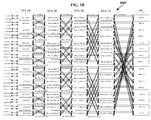
- FIG. 3B is a folded version of the multi-link multi-stage network 300 A shown in FIG. 3A .
- the network 300 B in FIG. 3B shows input stage 110 and output stage 120 are placed together. That is input switch IS 1 and output switch OS 1 are placed together, input switch IS 2 and output switch OS 2 are placed together, and similarly input switch IS 16 and output switch OS 16 are placed together.
- All the right going middle links ⁇ i.e., inlet links IL 1 -IL 32 and middle links ML( 1 , 1 )-ML( 1 , 64 ) ⁇ correspond to input switches IS 1 -IS 16
- all the left going middle links ⁇ i.e., middle links ML( 7 , 1 )-ML( 7 , 64 ) and outlet links OL 1 -OL 32 ⁇ correspond to output switches OS 1 -OS 16 .
- the switch input switch IS 1 and output switch OS 1 are placed together; so input switch IS 1 is implemented as two by four switch with the inlet links IL 1 and IL 2 being the inputs of the input switch IS 1 and middle links ML( 1 , 1 )-ML( 1 , 4 ) being the outputs of the input switch IS 1 ; and output switch OS 1 is implemented as four by two switch with the middle links ML( 8 , 1 ), ML( 8 , 2 ), ML( 8 , 7 ) and ML( 8 , 8 ) being the inputs of the output switch OS 1 and outlet links OL 1 -OL 2 being the outputs of the output switch OS 1 .
- all the switches that are placed together are implemented as separate switches.
- Block 1 _ 2 there are sixteen blocks namely Block 1 _ 2 , Block 3 _ 4 , Block 5 _ 6 , Block 7 _ 8 , Block 9 _ 10 , Block 11 _ 12 , Block 13 _ 14 , Block 15 _ 16 , Block 17 _ 18 , Block 19 _ 20 , Block 21 _ 22 , Block 23 _ 24 , Block 25 _ 26 , Block 27 _ 28 , Block 29 _ 30 , and Block 31 _ 32 .
- Each block implements all the switches in one row of the network 300 B of FIG. 3B , one of the key aspects of the current invention.
- Block 1 _ 2 implements the input switch IS 1 , output Switch OS 1 , middle switch MS( 1 , 1 ), middle switch MS( 7 , 1 ), middle switch MS( 2 , 1 ), middle switch MS( 6 , 1 ), middle switch MS( 3 , 1 ), middle switch MS( 5 , 1 ), and middle switch MS( 4 , 1 ).
- Input switch IS 1 and output switch OS 1 together are denoted as switch 1 ;
- Middle switch MS( 1 , 1 ) and middle switch MS( 7 , 1 ) together are denoted by switch 2 ;
- Middle switch MS( 2 , 1 ) and middle switch MS( 6 , 1 ) together are denoted by switch 3 ;
- Middle switch MS( 3 , 1 ) and middle switch MS( 5 , 1 ) together are denoted by switch 4 ;
- middle switch MS( 4 , 1 ) is denoted by switch 5 .
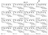
- inlet links IL 1 -IL 2 , outlet links OL 1 -OL 2 , middle link ML( 1 , 1 ), middle link ML( 1 , 2 ), middle link ML( 8 , 1 ), middle link ML( 8 , 2 ), middle link ML( 2 , 1 ), middle link ML( 2 , 2 ), middle link ML( 7 , 1 ), middle link ML( 7 , 2 ), middle link ML( 3 , 1 ), middle link ML( 3 , 2 ), middle link ML( 6 , 1 ), middle link ML( 6 , 2 ), middle link ML( 4 , 1 ), middle link ML( 4 , 2 ), middle link ML( 5 , 1 ) and middle link ML( 5 , 2 ) are illustrated in layout 300 C of FIG. 3C .
- each block in addition to the switches there may be Configurable Logic Blocks (CLB) or any arbitrary digital circuit or sub-integrated circuit block depending on the applications in different embodiments.
- CLB Configurable Logic Blocks
- Top-left quadrant implements Block 1 _ 2 , Block 3 _ 4 , Block 5 _ 6 , and Block 7 _ 8 .
- Bottom-left quadrant implements Block 9 _ 10 , Block 11 _ 12 , Block 13 _ 14 , and Block 15 _ 16 .
- Top-right quadrant implements Block 25 _ 26 , Block 27 _ 28 , Block 29 _ 30 , and Block 31 _ 32 .
- Bottom-right quadrant implements Block 17 _ 18 , Block 19 _ 20 , Block 21 _ 22 , and Block 23 _ 24 .
- each quadrant there are four sub-quadrants.
- there are four sub-quadrants namely top-left sub-quadrant, bottom-left sub-quadrant, top-right sub-quadrant and bottom-right sub-quadrant.
- Top-left sub-quadrant of top-left quadrant implements Block 1 _ 2 .
- Bottom-left sub-quadrant of top-left quadrant implements Block 3 _ 4 .
- Top-right sub-quadrant of top-left quadrant implements Block 7 _ 8 .
- Finally bottom-right sub-quadrant of top-left quadrant implements Block 5 _ 6 .
- top-left quadrant there are two sub-halves namely left-sub-half and right-sub-half.
- Left-sub-half of top-left quadrant implements Block 1 _ 2 and Block 3 _ 4 .
- Right-sub-half of top-left quadrant implements Block 7 _ 8 and Block 5 _ 6 .
- V fold-mlink N 1 , N 2 , d, s
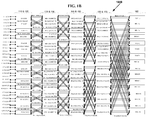
- Layout 300 D of FIG. 3D illustrates the inter-block links (in the layout 300 C of FIG. 3C all the cross middle links are inter-block links) between switches 1 and 2 of each block.
- middle links ML( 1 , 3 ), ML( 1 , 4 ), ML( 8 , 7 ), and ML( 8 , 8 ) are connected between switch 1 of Block 1 _ 2 and switch 2 of Block 3 _ 4 .
- middle links ML( 1 , 7 ), ML( 1 , 8 ), ML( 8 , 3 ), and ML( 8 , 4 ) are connected between switch 2 of Block 1 _ 2 and switch 1 of Block 3 _ 4 .
- inter-block links are implemented as two different tracks (for example middle links ML( 1 , 4 ) and ML( 8 , 8 ) are implemented as two different tracks); or in an alternative embodiment inter-block links are implemented as a time division multiplexed single track (for example middle links ML( 1 , 4 ) and ML( 8 , 8 ) are implemented as a time division multiplexed single track).
- Layout 300 E of FIG. 3E illustrates the inter-block links between switches 2 and 3 of each block.
- middle links ML( 2 , 3 ), ML( 2 , 4 ), ML( 7 , 11 ), and ML( 7 , 12 ) are connected between switch 2 of Block 1 _ 2 and switch 3 of Block 3 _ 4 .
- middle links ML( 2 , 11 ), ML( 2 , 12 ), ML( 7 , 3 ), and ML( 7 , 4 ) are connected between switch 3 of Block 1 _ 2 and switch 2 of Block 3 _ 4 .
- the inter-block links illustrated in layout 300 E of FIG. 3E can be implemented as diagonal tracks in one embodiment.
- inter-block links are implemented as two different tracks (for example middle links ML( 2 , 12 ) and ML( 7 , 4 ) are implemented as two different tracks); or in an alternative embodiment inter-block links are implemented as a time division multiplexed single track (for example middle links ML( 2 , 12 ) and ML( 7 , 4 ) are implemented as a time division multiplexed single track).
- Layout 300 F of FIG. 3F illustrates the inter-block links between switches 3 and 4 of each block.
- middle links ML( 3 , 3 ), ML( 3 , 4 ), ML( 6 , 19 ), and ML( 6 , 20 ) are connected between switch 3 of Block 1 _ 2 and switch 4 of Block 3 _ 4 .
- middle links ML( 3 , 19 ), ML( 3 , 20 ), ML( 6 , 3 ), and ML( 6 , 4 ) are connected between switch 4 of Block 1 _ 2 and switch 3 of Block 3 _ 4 .
- the inter-block links illustrated in layout 300 F of FIG. 3F can be implemented as vertical tracks in one embodiment.
- inter-block links are implemented as two different tracks (for example middle links ML( 3 , 4 ) and ML( 6 , 20 ) are implemented as two different tracks); or in an alternative embodiment inter-block links are implemented as a time division multiplexed single track (for example middle links ML( 3 , 4 ) and ML( 6 , 20 ) are implemented as a time division multiplexed single track).
- Layout 300 G of FIG. 3G illustrates the inter-block links between switches 4 and 5 of each block.
- middle links ML( 4 , 3 ), ML( 4 , 4 ), ML( 5 , 35 ), and ML( 5 , 36 ) are connected between switch 4 of Block 1 _ 2 and switch 5 of Block 3 _ 4 .
- middle links ML( 4 , 35 ), ML( 4 , 36 ), ML( 5 , 3 ), and ML( 5 , 4 ) are connected between switch 5 of Block 1 _ 2 and switch 4 of Block 3 _ 4 .
- the inter-block links illustrated in layout 300 G of FIG. 3G can be implemented as horizontal tracks in one embodiment.
- inter-block links are implemented as two different tracks (for example middle links ML( 4 , 4 ) and ML( 5 , 36 ) are implemented as two different tracks); or in an alternative embodiment inter-block links are implemented as a time division multiplexed single track (for example middle links ML( 4 , 4 ) and ML( 5 , 36 ) are implemented as a time division multiplexed single track).
- the complete layout for the network 300 B of FIG. 3B is given by combining the links in layout diagrams of 300 C, 300 D, 300 E, 300 F, and 300 G.
- the inter-block links between switch 1 and switch 2 are vertical tracks as shown in layout 300 D of FIG. 3D ;
- the inter-block links between switch 2 and switch 3 are horizontal tracks as shown in layout 300 E of FIG. 3E ;
- the inter-block links between switch 3 and switch 4 are vertical tracks as shown in layout 300 F of FIG. 3F ;
- the inter-block links between switch 4 and switch 5 are horizontal tracks as shown in layout 300 G of FIG. 3G .
- the pattern is either vertical tracks, horizontal tracks or diagonal tracks. It continues recursively for larger networks of N>32 as will be illustrated later.
- All the switches in one row of the multi-stage network 300 B are implemented in a single block. 2) The blocks are placed in such a way that all the inter-block links are either horizontal tracks, vertical tracks or diagonal tracks; 3) The length of the longest wire is about half of the width (or length) of the complete layout (For example middle link ML( 4 , 4 ) is about half the width of the complete layout.);
- the layout 300 C in FIG. 3C can be recursively extended for any arbitrarily large generalized folded multi link multi-stage network V fold-mlink (N 1 , N 2 , d, s).
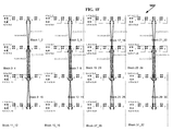
- There are four super-quadrants in layout 300 H namely top-left super-quadrant, bottom-left super-quadrant, top-right super-quadrant, bottom-right super-quadrant.
- Total number of blocks in the layout 300 H is sixty four.
- Top-left super-quadrant implements the blocks from block 1 _ 2 to block 31 _ 32 .
- Each block in all the super-quadrants has two more switches namely switch 6 and switch 7 in addition to the switches [ 1 - 5 ] illustrated in layout 300 C of FIG. 3C .
- the inter-block link connection topology is the exactly the same between the switches 1 and 2 ; switches 2 and 3 ; switches 3 and 4 ; switches 4 and 5 as it is shown in the layouts of FIG. 3D , FIG. 3E , FIG. 3F , and FIG. 3G respectively.
- Bottom-left super-quadrant implements the blocks from block 33 _ 34 to block 63 _ 64 .
- Top-right super-quadrant implements the blocks from block 65 _ 66 to block 95 _ 96 .
- bottom-right super-quadrant implements the blocks from block 97 _ 98 to block 127 _ 128 .
- the inter-block link connection topology is the exactly the same between the switches 1 and 2 ; switches 2 and 3 ; switches 3 and 4 ; switches 4 and 5 as that of the top-left super-quadrant.
- the inter-block links connecting the switch 5 and switch 6 will be vertical tracks between the corresponding switches of top-left super-quadrant and bottom-left super-quadrant. And similarly the inter-block links connecting the switch 5 and switch 6 will be vertical tracks between the corresponding switches of top-right super-quadrant and bottom-right super-quadrant.
- the inter-block links connecting the switch 6 and switch 7 will be horizontal tracks between the corresponding switches of top-left super-quadrant and top-right super-quadrant. And similarly the inter-block links connecting the switch 6 and switch 7 will be horizontal tracks between the corresponding switches of bottom-left super-quadrant and bottom-right super-quadrant.
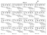
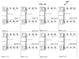
- Layout diagram 400 C of FIG. 4C is another embodiment for the generalized folded multi-link multi-stage network V fold-mlink (N 1 , N 2 , d, s) diagram 100 B in FIG. 1B .
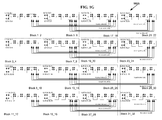
- Block 1 _ 2 there are sixteen blocks namely Block 1 _ 2 , Block 3 _ 4 , Block 5 _ 6 , Block 7 _ 8 , Block 9 _ 10 , Block 11 _ 12 , Block 13 _ 14 , Block 15 _ 16 , Block 17 _ 18 , Block 19 _ 20 , Block 21 _ 22 , Block 23 _ 24 , Block 25 _ 26 , Block 27 _ 28 , Block 29 _ 30 , and Block 31 _ 32 .
- Each block implements all the switches in one row of the network 100 B of FIG. 1B , one of the key aspects of the current invention.
- Block 1 _ 2 implements the input switch IS 1 , output Switch OS 1 , middle switch MS( 1 , 1 ), middle switch MS( 7 , 1 ), middle switch MS( 2 , 1 ), middle switch MS( 6 , 1 ), middle switch MS( 3 , 1 ), middle switch MS( 5 , 1 ), and middle switch MS( 4 , 1 ).
- Input switch IS 1 and output switch OS 1 together are denoted as switch 1 ;
- Middle switch MS( 1 , 1 ) and middle switch MS( 7 , 1 ) together are denoted by switch 2 ;
- Middle switch MS( 2 , 1 ) and middle switch MS( 6 , 1 ) together are denoted by switch 3 ;
- Middle switch MS( 3 , 1 ) and middle switch MS( 5 , 1 ) together are denoted by switch 4 ;
- middle switch MS( 4 , 1 ) is denoted by switch 5 .
- inlet links IL 1 -IL 2 , outlet links OL 1 -OL 2 , middle link ML( 1 , 1 ), middle link ML( 1 , 2 ), middle link ML( 8 , 1 ), middle link ML( 8 , 2 ), middle link ML( 2 , 1 ), middle link ML( 2 , 2 ), middle link ML( 7 , 1 ), middle link ML( 7 , 2 ), middle link ML( 3 , 1 ), middle link ML( 3 , 2 ), middle link ML( 6 , 1 ), middle link ML( 6 , 2 ), middle link ML( 4 , 1 ), middle link ML( 4 , 2 ), middle link ML( 5 , 1 ) and middle link ML( 5 , 2 ) are illustrated in layout 400 C of FIG. 4C .
- each block in addition to the switches there may be Configurable Logic Blocks (CLB) or any arbitrary digital circuit or sub-integrated circuit block depending on the applications in different embodiments.
- CLB Configurable Logic Blocks
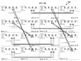
- the topology of the layout 400 C in FIG. 4C is a ring.
- the corresponding blocks are also physically neighbors in layout diagram 400 C of FIG. 4C .
- the topmost row is also logically considered as neighbor to the bottommost row.
- Block 1 _ 2 (implementing the switches belonging to a row in diagram 100 B of FIG. 1B ) has Block 3 _ 4 as neighbor since Block 3 _ 4 implements the switches in its neighboring row.
- Block 1 _ 2 also has Block 31 _ 32 as neighbor since Block 1 _ 2 implements topmost row of switches and Block 31 _ 32 implements bottommost row of switches in diagram 100 B of FIG. 1B .
- Layout 400 B of FIG. 4B illustrates the inter-block links (in the layout 400 A of FIG. 4A all the cross middle links are inter-block links) between switches 1 and 2 of each block.
- middle links ML( 1 , 3 ), ML( 1 , 4 ), ML( 8 , 7 ), and ML( 8 , 8 ) are connected between switch 1 of Block 1 _ 2 and switch 2 of Block 3 _ 4 .
- middle links ML( 1 , 7 ), ML( 1 , 8 ), ML( 8 , 3 ), and ML( 8 , 4 ) are connected between switch 2 of Block 1 _ 2 and switch 1 of Block 3 _ 4 .
- inter-block links are implemented as vertical tracks or horizontal tracks or diagonal tracks.
- inter-block links are implemented as two different tracks (for example middle links ML( 1 , 4 ) and ML( 8 , 8 ) are implemented as two different tracks); or in an alternative embodiment inter-block links are implemented as a time division multiplexed single track (for example middle links ML( 1 , 4 ) and ML( 8 , 8 ) are implemented as a time division multiplexed single track).
- Layout 400 C of FIG. 4C illustrates the inter-block links between switches 2 and 3 of each block.
- middle links ML( 2 , 3 ), ML( 2 , 4 ), ML( 7 , 11 ), and ML( 7 , 12 ) are connected between switch 2 of Block 1 _ 2 and switch 3 of Block 3 _ 4 .
- middle links ML( 2 , 11 ), ML( 2 , 12 ), ML( 7 , 3 ), and ML( 7 , 4 ) are connected between switch 3 of Block 1 _ 2 and switch 2 of Block 3 _ 4 .
- the inter-block links illustrated in layout 400 C of FIG. 4C are implemented as vertical tracks or horizontal tracks or diagonal tracks.
- inter-block links are implemented as two different tracks (for example middle links ML( 2 , 12 ) and ML( 7 , 4 ) are implemented as two different tracks); or in an alternative embodiment inter-block links are implemented as a time division multiplexed single track (for example middle links ML( 2 , 12 ) and ML( 7 , 4 ) are implemented as a time division multiplexed single track).
- Layout 400 D of FIG. 4D illustrates the inter-block links between switches 3 and 4 of each block.
- middle links ML( 3 , 3 ), ML( 3 , 4 ), ML( 6 , 19 ), and ML( 6 , 20 ) are connected between switch 3 of Block 1 _ 2 and switch 4 of Block 3 _ 4 .
- middle links ML( 3 , 19 ), ML( 3 , 20 ), ML( 6 , 3 ), and ML( 6 , 4 ) are connected between switch 4 of Block 1 _ 2 and switch 3 of Block 3 _ 4 .
- the inter-block links illustrated in layout 400 D of FIG. 4D are implemented as vertical tracks or horizontal tracks or diagonal tracks.
- inter-block links are implemented as two different tracks (for example middle links ML( 3 , 4 ) and ML( 6 , 20 ) are implemented as two different tracks); or in an alternative embodiment inter-block links are implemented as a time division multiplexed single track (for example middle links ML( 3 , 4 ) and ML( 6 , 20 ) are implemented as a time division multiplexed single track).
- Layout 400 E of FIG. 4E illustrates the inter-block links between switches 4 and 5 of each block.
- middle links ML( 4 , 3 ), ML( 4 , 4 ), ML( 5 , 35 ), and ML( 5 , 36 ) are connected between switch 4 of Block 1 _ 2 and switch 5 of Block 3 _ 4 .
- middle links ML( 4 , 35 ), ML( 4 , 36 ), ML( 5 , 3 ), and ML( 5 , 4 ) are connected between switch 5 of Block 1 _ 2 and switch 4 of Block 3 _ 4 .
- the inter-block links illustrated in layout 400 E of FIG. 4E are implemented as vertical tracks or horizontal tracks or diagonal tracks.
- inter-block links are implemented as two different tracks (for example middle links ML( 4 , 4 ) and ML( 5 , 36 ) are implemented as two different tracks); or in an alternative embodiment inter-block links are implemented as a time division multiplexed single track (for example middle links ML( 4 , 4 ) and ML( 5 , 36 ) are implemented as a time division multiplexed single track).
- the complete layout for the network 100 B of FIG. 1B is given by combining the links in layout diagrams of 400 A, 400 B, 400 C, 400 D, and 400 E.
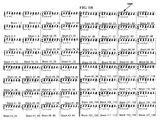
- Layout diagram 400 C 1 of FIG. 4 C 1 is another embodiment for the generalized folded multi-link multi-stage network V fold-mlink (N 1 , N 2 , d, s) diagram 100 B in FIG. 1B .
- layout 400 C 1 of FIG. 4 C 1 there are sixteen blocks namely Block 1 _ 2 , Block 3 _ 4 , Block 5 _ 6 , Block 7 _ 8 , Block 9 _ 10 , Block 11 _ 12 , Block 13 _ 14 , Block 15 _ 16 , Block 17 _ 18 , Block 19 _ 20 , Block 21 _ 22 , Block 23 _ 24 , Block 25 _ 26 , Block 27 _ 28 , Block 29 _ 30 , and Block 31 _ 32 .
- Block 1 _ 2 implements the input switch IS 1 , output Switch OS 1 , middle switch MS( 1 , 1 ), middle switch MS( 7 , 1 ), middle switch MS( 2 , 1 ), middle switch MS( 6 , 1 ), middle switch MS( 3 , 1 ), middle switch MS( 5 , 1 ), and middle switch MS( 4 , 1 ).
- Input switch IS 1 and output switch OS 1 together are denoted as switch 1 ;
- Middle switch MS( 1 , 1 ) and middle switch MS( 7 , 1 ) together are denoted by switch 2 ;
- Middle switch MS( 2 , 1 ) and middle switch MS( 6 , 1 ) together are denoted by switch 3 ;
- Middle switch MS( 3 , 1 ) and middle switch MS( 5 , 1 ) together are denoted by switch 4 ;
- middle switch MS( 4 , 1 ) is denoted by switch 5 .
- inlet links IL 1 -IL 2 , outlet links OL 1 -OL 2 , middle link ML( 1 , 1 ), middle link ML( 1 , 2 ), middle link ML( 8 , 1 ), middle link ML( 8 , 2 ), middle link ML( 2 , 1 ), middle link ML( 2 , 2 ), middle link ML( 7 , 1 ), middle link ML( 7 , 2 ), middle link ML( 3 , 1 ), middle link ML( 3 , 2 ), middle link ML( 6 , 1 ), middle link ML( 6 , 2 ), middle link ML( 4 , 1 ), middle link ML( 4 , 2 ), middle link ML( 5 , 1 ) and middle link ML( 5 , 2 ) are illustrated in layout 400 C 1 of FIG. 4 C 1 .
- each block in addition to the switches there may be Configurable Logic Blocks (CLB) or any arbitrary digital circuit or sub-integrated circuit block depending on the applications in different embodiments.
- CLB Configurable Logic Blocks
- the topology of the layout 400 C 1 in FIG. 4 C 1 is another embodiment of ring layout topology.
- the corresponding blocks are also physically neighbors in layout diagram 400 C of FIG. 4C .
- the topmost row is also logically considered as neighbor to the bottommost row.
- Block 1 _ 2 (implementing the switches belonging to a row in diagram 100 B of FIG.
- Block 1B has Block 3 _ 4 as neighbor since Block 3 _ 4 implements the switches in its neighboring row.
- Block 1 _ 2 also has Block 31 _ 32 as neighbor since Block 1 _ 2 implements topmost row of switches and Block 31 _ 32 implements bottommost row of switches in diagram 100 B of FIG. 1B .
- FIG. 5 A 1 illustrates the diagram of 500 A 1 which is a typical two by two switch with two inlet links namely IL 1 and IL 2 , and two outlet links namely OL 1 and OL 2 .
- the two by two switch also implements four crosspoints namely CP( 1 , 1 ), CP( 1 , 2 ), CP( 2 , 1 ) and CP( 2 , 2 ) as illustrated in FIG. 5 A 1 .
- the diagram of 500 A 1 may the implementation of middle switch MS( 1 , 1 ) of the diagram 100 K of FIG.
- inlet link IL 1 of diagram 500 A 1 corresponds to middle link ML( 1 , 1 ) of diagram 100 K
- inlet link IL 2 of diagram 500 A 1 corresponds to middle link ML( 1 , 7 ) of diagram 100 K
- outlet link OL 1 of diagram 500 A 1 corresponds to middle link ML( 2 , 1 ) of diagram 100 K
- outlet link OL 2 of diagram 500 A 1 corresponds to middle link ML( 2 , 3 ) of diagram 100 K.
- FIG. 5 A 2 illustrates the detailed diagram 500 A 2 for the implementation of the diagram 500 A 1 in programmable integrated circuit embodiments.
- Each crosspoint is implemented by a transistor coupled between the corresponding inlet link and outlet link, and a programmable cell in programmable integrated circuit embodiments.
- crosspoint CP( 1 , 1 ) is implemented by transistor C( 1 , 1 ) coupled between inlet link IL 1 and outlet link OL 1 , and programmable cell P( 1 , 1 );
- crosspoint CP( 1 , 2 ) is implemented by transistor C( 1 , 2 ) coupled between inlet link IL 1 and outlet link OL 2 , and programmable cell P( 1 , 2 );
- crosspoint CP( 2 , 1 ) is implemented by transistor C( 2 , 1 ) coupled between inlet link IL 2 and outlet link OL 1 , and programmable cell P( 2 , 1 );
- crosspoint CP( 2 , 2 ) is implemented by transistor C( 2 , 2 ) coupled between inlet link IL 2 and outlet link OL 2 , and programmable cell P( 2 , 2 ).
- the programmable cell If the programmable cell is programmed ON, the corresponding transistor couples the corresponding inlet link and outlet link. If the programmable cell is programmed OFF, the corresponding inlet link and outlet link are not connected. For example if the programmable cell P( 1 , 1 ) is programmed ON, the corresponding transistor C( 1 , 1 ) couples the corresponding inlet link IL 1 and outlet link OL 1 . If the programmable cell P( 1 , 1 ) is programmed OFF, the corresponding inlet link IL 1 and outlet link OL 1 are not connected. In volatile programmable integrated circuit embodiments the programmable cell may be an SRAM (Static Random Address Memory) cell.
- SRAM Static Random Address Memory
- the programmable cell may be a Flash memory cell.
- the programmable integrated circuit embodiments may implement field programmable logic arrays (FPGA) devices, or programmable Logic devices (PLD), or Application Specific Integrated Circuits (ASIC) embedded with programmable logic circuits or 3D-FPGAs.
- FPGA field programmable logic arrays
- PLD programmable Logic devices
- ASIC Application Specific Integrated Circuits
- FIG. 5 A 2 also illustrates a buffer B 1 on inlet link IL 2 .
- the signals driven along inlet link IL 2 are amplified by buffer B 1 .
- Buffer B 1 can be inverting or non-inverting buffer. Buffers such as B 1 are used to amplify the signal in links which are usually long.
- FIG. 5 A 3 illustrates the detailed diagram 500 A 3 for the implementation of the diagram 500 A 1 in one-time programmable integrated circuit embodiments.
- Each crosspoint is implemented by a via coupled between the corresponding inlet link and outlet link in one-time programmable integrated circuit embodiments.
- crosspoint CP( 1 , 1 ) is implemented by via V( 1 , 1 ) coupled between inlet link IL 1 and outlet link OL 1 ;
- crosspoint CP( 1 , 2 ) is implemented by via V( 1 , 2 ) coupled between inlet link IL 1 and outlet link OL 2 ;
- crosspoint CP( 2 , 1 ) is implemented by via V( 2 , 1 ) coupled between inlet link IL 2 and outlet link OL 1 ;
- crosspoint CP( 2 , 2 ) is implemented by via V( 2 , 2 ) coupled between inlet link IL 2 and outlet link OL 2 .
- the via V( 1 , 1 ) is programmed ON, and the corresponding inlet link IL 1 and outlet link OL 1 are connected as denoted by thick circle at the intersection of inlet link IL 1 and outlet link OL 1 ;
- the via V( 2 , 2 ) is programmed ON, and the corresponding inlet link IL 2 and outlet link OL 2 are connected as denoted by thick circle at the intersection of inlet link IL 2 and outlet link OL 2 ;
- the via V( 1 , 2 ) is programmed OFF, and the corresponding inlet link IL 1 and outlet link OL 2 are not connected as denoted by the absence of thick circle at the intersection of in
- FIG. 5 A 4 illustrates the detailed diagram 500 A 4 for the implementation of the diagram 500 A 1 in Integrated Circuit Placement and Route embodiments.
- the switch and crosspoints are actually virtual.
- the concept of virtual switch and virtual crosspoint using the embodiments disclosed in the current invention reduces the number of required wires, wire length needed to connect the inputs and outputs of different netlists and the time required by the tool for placement and route of netlists in the integrated circuit.
- Each virtual crosspoint is used to either to hardwire or provide no connectivity between the corresponding inlet link and outlet link.
- crosspoint CP( 1 , 1 ) is implemented by direct connect point DCP( 1 , 1 ) to hardwire (i.e., to permanently connect) inlet link IL 1 and outlet link OL 1 which is denoted by the thick circle at the intersection of inlet link IL 1 and outlet link OL 1 ;
- crosspoint CP( 2 , 2 ) is implemented by direct connect point DCP( 2 , 2 ) to hardwire inlet link IL 2 and outlet link OL 2 which is denoted by the thick circle at the intersection of inlet link IL 2 and outlet link OL 2 .
- the diagram 500 A 4 does not show direct connect point DCP( 1 , 2 ) and direct connect point DCP( 1 , 3 ) since they are not needed and in the hardware implementation they are eliminated.
- inlet link IL 1 needs to be connected to outlet link OL 1 and inlet link IL 1 does not need to be connected to outlet link OL 2 .
- inlet link IL 2 needs to be connected to outlet link OL 2 and inlet link IL 2 does not need to be connected to outlet link OL 1 .
- the absence of direct connect point DCP( 2 , 1 ) illustrates there is no need to connect inlet link IL 2 and outlet link OL 1 .
Abstract
Description
- This application is related to and claims priority of the PCT Application Serial No. PCT/US08/64605 entitled “VLSI LAYOUTS OF FULLY CONNECTED GENERALIZED NETWORKS” by Venkat Konda assigned to the same assignee as the current application, filed May 22, 2008, and the U.S. Provisional Patent Application Ser. No. 60/940,394 entitled “VLSI LAYOUTS OF FULLY CONNECTED GENERALIZED NETWORKS” by Venkat Konda assigned to the same assignee as the current application, filed May 25, 2007.
- This application is related to and incorporates by reference in its entirety the U.S. application Ser. No. 12/530,207 entitled “FULLY CONNECTED GENERALIZED MULTI-STAGE NETWORKS” by Venkat Konda assigned to the same assignee as the current application, filed Sep. 6, 2009, the PCT Application Serial No. PCT/US08/56064 entitled “FULLY CONNECTED GENERALIZED MULTI-STAGE NETWORKS” by Venkat Konda assigned to the same assignee as the current application, filed Mar. 6, 2008, the U.S. Provisional Patent Application Ser. No. 60/905,526 entitled “LARGE SCALE CROSSPOINT REDUCTION WITH NONBLOCKING UNICAST & MULTICAST IN ARBITRARILY LARGE MULTI-STAGE NETWORKS” by Venkat Konda assigned to the same assignee as the current application, filed Mar. 6, 2007, and the U.S. Provisional Patent Application Ser. No. 60/940,383 entitled “FULLY CONNECTED GENERALIZED MULTI-STAGE NETWORKS” by Venkat Konda assigned to the same assignee as the current application, filed May 25, 2007.
- This application is related to and incorporates by reference in its entirety the US Patent Application Docket No. V-0038US entitled “FULLY CONNECTED GENERALIZED BUTTERFLY FAT TREE NETWORKS” by Venkat Konda assigned to the same assignee as the current application filed concurrently, the PCT Application Serial No. PCT/US08/64603 entitled “FULLY CONNECTED GENERALIZED BUTTERFLY FAT TREE NETWORKS” by Venkat Konda assigned to the same assignee as the current application, filed May 22, 2008, the U.S. Provisional Patent Application Ser. No. 60/940, 387 entitled “FULLY CONNECTED GENERALIZED BUTTERFLY FAT TREE NETWORKS” by Venkat Konda assigned to the same assignee as the current application, filed May 25, 2007, and the U.S. Provisional Patent Application Ser. No. 60/940, 390 entitled “FULLY CONNECTED GENERALIZED MULTI-LINK BUTTERFLY FAT TREE NETWORKS” by Venkat Konda assigned to the same assignee as the current application, filed May 25, 2007.
- This application is related to and incorporates by reference in its entirety the US Patent Application Docket No. V-0039US entitled “FULLY CONNECTED GENERALIZED MULTI-LINK MULTI-STAGE NETWORKS” by Venkat Konda assigned to the same assignee as the current application filed concurrently, the PCT Application Serial No. PCT/US08/64604 entitled “FULLY CONNECTED GENERALIZED MULTI-LINK MULTI-STAGE NETWORKS” by Venkat Konda assigned to the same assignee as the current application, filed May 22, 2008, the U.S. Provisional Patent Application Ser. No. 60/940, 389 entitled “FULLY CONNECTED GENERALIZED REARRANGEABLY NONBLOCKING MULTI-LINK MULTI-STAGE NETWORKS” by Venkat Konda assigned to the same assignee as the current application, filed May 25, 2007, the U.S. Provisional Patent Application Ser. No. 60/940, 391 entitled “FULLY CONNECTED GENERALIZED FOLDED MULTI-STAGE NETWORKS” by Venkat Konda assigned to the same assignee as the current application, filed May 25, 2007 and the U.S. Provisional Patent Application Ser. No. 60/940,392 entitled “FULLY CONNECTED GENERALIZED STRICTLY NONBLOCKING MULTI-LINK MULTI-STAGE NETWORKS” by Venkat Konda assigned to the same assignee as the current application, filed May 25, 2007.
- This application is related to and incorporates by reference in its entirety the U.S. Provisional Patent Application Ser. No. 61/252, 603 entitled “VLSI LAYOUTS OF FULLY CONNECTED NETWORKS WITH LOCALITY EXPLOITATION” by Venkat Konda assigned to the same assignee as the current application, filed Oct. 16, 2009.
- This application is related to and incorporates by reference in its entirety the U.S. Provisional Patent Application Ser. No. 61/252, 609 entitled “VLSI LAYOUTS OF FULLY CONNECTED GENERALIZED AND PYRAMID NETWORKS” by Venkat Konda assigned to the same assignee as the current application, filed Oct. 16, 2009.
- Multi-stage interconnection networks such as Benes networks and butterfly fat tree networks are widely useful in telecommunications, parallel and distributed computing. However VLSI layouts, known in the prior art, of these interconnection networks in an integrated circuit are inefficient and complicated.
- Other multi-stage interconnection networks including butterfly fat tree networks, Banyan networks, Batcher-Banyan networks, Baseline networks, Delta networks, Omega networks and Flip networks have been widely studied particularly for self routing packet switching applications. Also Benes Networks with radix of two have been widely studied and it is known that Benes Networks of radix two are shown to be built with back to back baseline networks which are rearrangeably nonblocking for unicast connections.
- The most commonly used VLSI layout in an integrated circuit is based on a two-dimensional grid model comprising only horizontal and vertical tracks. An intuitive interconnection network that utilizes two-dimensional grid model is 2D Mesh Network and its variations such as segmented mesh networks. Hence routing networks used in VLSI layouts are typically 2D mesh networks and its variations. However Mesh Networks require large scale cross points typically with a growth rate of O(N2) where N is the number of computing elements, ports, or logic elements depending on the application.
- Multi-stage interconnection with a growth rate of O(N×log N) requires significantly small number of cross points. U.S. Pat. No. 6,185,220 entitled “Grid Layouts of Switching and Sorting Networks” granted to Muthukrishnan et al. describes a VLSI layout using existing VLSI grid model for Benes and Butterfly networks. U.S. Pat. No. 6,940,308 entitled “Interconnection Network for a Field Programmable Gate Array” granted to Wong describes a VLSI layout where switches belonging to lower stage of Benes Network are layed out close to the logic cells and switches belonging to higher stages are layed out towards the center of the layout.
- Due to the inefficient and in some cases impractical VLSI layout of Benes and butterfly fat tree networks on a semiconductor chip, today mesh networks and segmented mesh networks are widely used in the practical applications such as field programmable gate arrays (FPGAs), programmable logic devices (PLDs), and parallel computing interconnects. The prior art VLSI layouts of Benes and butterfly fat tree networks and VLSI layouts of mesh networks and segmented mesh networks require large area to implement the switches on the chip, large number of wires, longer wires, with increased power consumption, increased latency of the signals which effect the maximum clock speed of operation. Some networks may not even be implemented practically on a chip due to the lack of efficient layouts.
- When large scale sub-integrated circuit blocks with inlet and outlet links are layed out in an integrated circuit device in a two-dimensional grid arrangement, (for example in an FPGA where the sub-integrated circuit blocks are Lookup Tables) the most intuitive routing network is a network that uses horizontal and vertical links only (the most often used such a network is one of the variations of a 2D Mesh network). A direct embedding of a generalized multi-stage network on to a 2D Mesh network is neither simple nor efficient.
- In accordance with the invention, VLSI layouts of generalized multi-stage networks for broadcast, unicast and multicast connections are presented using only horizontal and vertical links The VLSI layouts employ shuffle exchange links where outlet links of cross links from switches in a stage in one sub-integrated circuit block are connected to inlet links of switches in the succeeding stage in another sub-integrated circuit block so that said cross links are either vertical links or horizontal and vice versa. In one embodiment the sub-integrated circuit blocks are arranged in a hypercube arrangement in a two-dimensional plane. The VLSI layouts exploit the benefits of significantly lower cross points, lower signal latency, lower power and full connectivity with significantly fast compilation.
- The VLSI layouts presented are applicable to generalized multi-stage networks V(N1, N2, d, s), generalized folded multi-stage networks Vfold(N1, N2, d, s), generalized butterfly fat tree networks Vbft(N1, N2, d, s), generalized multi-link multi-stage networks Vmlink(N1, N2, d, s), generalized folded multi-link multi-stage networks Vfold-mlink(N1, N2, d, s), generalized multi-link butterfly fat tree networks Vmlink-bft(N1, N2, d, s), and generalized hypercube networks Vhcube(N1, N2, d, s) for s=1, 2, 3 or any number in general. The embodiments of VLSI layouts are useful in wide target applications such as FPGAs, CPLDs, pSoCs, ASIC placement and route tools, networking applications, parallel & distributed computing, and reconfigurable computing.
-
FIG. 1A is a diagram 100A of an exemplary symmetrical multi-link multi-stage network Vfold-mlink(N, d, s) having inverse Benes connection topology of nine stages with N=32, d=2 and s=2, strictly nonblocking network for unicast connections and rearrangeably nonblocking network for arbitrary fan-out multicast connections, in accordance with the invention. -
FIG. 1B is a diagram 100B of the equivalent symmetrical folded multi-link multi-stage network Vfold-mlink(N, d, s) of thenetwork 100A shown inFIG. 1A , having inverse Benes connection topology of five stages with N=32, d=2 and s=2, strictly nonblocking network for unicast connections and rearrangeably nonblocking network for arbitrary fan-out multicast connections, in accordance with the invention. -
FIG. 1C is a diagram 100C layout of the network Vfold-mlink(N, d, s) shown inFIG. 1B , in one embodiment, illustrating the connection links belonging with in each block only. -
FIG. 1D is a diagram 100D layout of the network Vfold-mlink(N, d, s) shown inFIG. 1B , in one embodiment, illustrating the connection links ML(1,i) for i=[1, 64] and ML(8,i) for i=[1,64]. -
FIG. 1E is a diagram 100E layout of the network Vfold-mlink(N, d, s) shown inFIG. 1B , in one embodiment, illustrating the connection links ML(2,i) for i=[1, 64] and ML(7,i) for i=[1,64]. -
FIG. 1F is a diagram 100F layout of the network Vfold-mlink(N, d, s) shown inFIG. 1B , in one embodiment, illustrating the connection links ML(3,i) for i=[1, 64] and ML(6,i) for i=[1,64]. -
FIG. 1G is a diagram 100G layout of the network Vfold-mlink(N, d, s) shown inFIG. 1B , in one embodiment, illustrating the connection links ML(4,i) for i=[1, 64] and ML(5,i) for i=[1,64]. -
FIG. 1H is a diagram 100H layout of a network Vfold-mlink(N, d, s) where N=128, d=2, and s=2, in one embodiment, illustrating the connection links belonging with in each block only. -
FIG. 11 is a diagram 100I detailed connections of BLOCK 1_2 in thenetwork layout 100C in one embodiment, illustrating the connection links going in and coming out when thelayout 100C is implementing V(N, d, s) or Vfold(N, d, s). -
FIG. 1J is a diagram 100J detailed connections of BLOCK 1_2 in thenetwork layout 100C in one embodiment, illustrating the connection links going in and coming out when thelayout 100C is implementing V(N, d, s) or Vfold(N, d, s). -
FIG. 1K is a diagram 100K detailed connections of BLOCK 1_2 in thenetwork layout 100C in one embodiment, illustrating the connection links going in and coming out when thelayout 100C is implementing V(N, d, s) or Vfold(N, d, s). - FIG. 1K1 is a diagram 100M1 detailed connections of BLOCK 1_2 in the
network layout 100C in one embodiment, illustrating the connection links going in and coming out when thelayout 100C is implementing V(N, d, s) or Vfold(N, d, s) for s=1. -
FIG. 1L is a diagram 100L detailed connections of BLOCK 1_2 in thenetwork layout 100C in one embodiment, illustrating the connection links going in and coming out when thelayout 100C is implementing V(N, d, s) or Vfold(N, d, s). - FIG. 1L1 is a diagram 100L1 detailed connections of BLOCK 1_2 in the
network layout 100C in one embodiment, illustrating the connection links going in and coming out when thelayout 100C is implementing V(N, d, s) or Vfold(N, d, s) for s=1. - FIG. 2A1 is a diagram 200A1 of an exemplary symmetrical multi-link multi-stage network Vfold-mlink(N, d, s) having inverse Benes connection topology of one stage with N=2, d=2 and s=2, strictly nonblocking network for unicast connections and rearrangeably nonblocking network for arbitrary fan-out multicast connections, in accordance with the invention. FIG. 2A2 is a diagram 200A2 of the equivalent symmetrical folded multi-link multi-stage network Vfold-mlink(N, d, s) of the network 200A1 shown in FIG. 2A1, having inverse Benes connection topology of one stage with N=2, d=2 and s=2, strictly nonblocking network for unicast connections and rearrangeably nonblocking network for arbitrary fan-out multicast connections, in accordance with the invention. FIG. 2A3 is a diagram 200A3 layout of the network Vfold-mlink(N, d, s) shown in FIG. 2A2, in one embodiment, illustrating all the connection links.
- FIG. 2B1 is a diagram 200B1 of an exemplary symmetrical multi-link multi-stage network Vfold-mlink(N, d, s) having inverse Benes connection topology of one stage with N=4, d=2 and s=2, strictly nonblocking network for unicast connections and rearrangeably nonblocking network for arbitrary fan-out multicast connections, in accordance with the invention. FIG. 2B2 is a diagram 200B2 of the equivalent symmetrical folded multi-link multi-stage network Vfold-mlink(N, d, s) of the network 200B1 shown in FIG. 2B1, having inverse Benes connection topology of one stage with N=4, d=2 and s=2, strictly nonblocking network for unicast connections and rearrangeably nonblocking network for arbitrary fan-out multicast connections, in accordance with the invention. FIG. 2B3 is a diagram 200B3 layout of the network Vfold-mlink(N, d, s) shown in FIG. 2B2, in one embodiment, illustrating the connection links belonging with in each block only. FIG. 2B4 is a diagram 200B4 layout of the network Vfold-mlink(N, d, s) shown in FIG. 2B2, in one embodiment, illustrating the connection links ML(1,i) for i=[1, 8] and ML(2,i) for i=[1,8].
- FIG. 2C11 is a diagram 200C11 of an exemplary symmetrical multi-link multi-stage network Vfold-mlink(N, d, s) having inverse Benes connection topology of one stage with N=8, d=2 and s=2, strictly nonblocking network for unicast connections and rearrangeably nonblocking network for arbitrary fan-out multicast connections, in accordance with the invention. FIG. 2C12 is a diagram 200C12 of the equivalent symmetrical folded multi-link multi-stage network Vfold-mlink(N, d, s) of the network 200C11 shown in FIG. 2C11, having inverse Benes connection topology of one stage with N=8, d=2 and s=2, strictly nonblocking network for unicast connections and rearrangeably nonblocking network for arbitrary fan-out multicast connections, in accordance with the invention.
- FIG. 2C21 is a diagram 200C21 layout of the network Vfold-mlink(N, d, s) shown in FIG. 2C12, in one embodiment, illustrating the connection links belonging with in each block only. FIG. 2C22 is a diagram 200C22 layout of the network Vfold-mlink(N, d, s) shown in FIG. 2C12, in one embodiment, illustrating the connection links ML(1,i) for i=[1, 16] and ML(4,i) for i=[1,16]. FIG. 2C23 is a diagram 200C23 layout of the network Vfold-mlink(N, d, s) shown in FIG. 2C12, in one embodiment, illustrating the connection links ML(2,i) for i=[1, 16] and ML(3,i) for i=[1,16].
- FIG. 2D1 is a diagram 200D1 of an exemplary symmetrical multi-link multi-stage network Vfold-mlink(N, d, s) having inverse Benes connection topology of one stage with N=16, d=2 and s=2, strictly nonblocking network for unicast connections and rearrangeably nonblocking network for arbitrary fan-out multicast connections, in accordance with the invention.
- FIG. 2D2 is a diagram 200D2 of the equivalent symmetrical folded multi-link multi-stage network Vfold-mlink(N, d, s) of the network 200D1 shown in FIG. 2D1, having inverse Benes connection topology of one stage with N=16, d=2 and s=2, strictly nonblocking network for unicast connections and rearrangeably nonblocking network for arbitrary fan-out multicast connections, in accordance with the invention.
- FIG. 2D3 is a diagram 200D3 layout of the network Vfold-mlink(N, d, s) shown in FIG. 2D2, in one embodiment, illustrating the connection links belonging with in each block only.
- FIG. 2D4 is a diagram 200D4 layout of the network Vfold-mlink(N, d, s) shown in FIG. 2D2, in one embodiment, illustrating the connection links ML(1,i) for i=[1, 32] and ML(6,i) for i=[1,32].
- FIG. 2D5 is a diagram 200D5 layout of the network Vfold-mlink(N, d, s) shown in FIG. 2D2, in one embodiment, illustrating the connection links ML(2,i) for i=[1, 32] and ML(5,i) for i=[1,32].
- FIG. 2D6 is a diagram 200D6 layout of the network Vfold-mlink(N, d, s) shown in FIG. 2D2, in one embodiment, illustrating the connection links ML(3,i) for i=[1, 32] and ML(4,i) for i=[1,32].
-
FIG. 3A is a diagram 300A of an exemplary symmetrical multi-link multi-stage network Vhcube(N, d, s) having inverse Benes connection topology of nine stages with N=32, d=2 and s=2, strictly nonblocking network for unicast connections and rearrangeably nonblocking network for arbitrary fan-out multicast connections, in accordance with the invention. -
FIG. 3B is a diagram 300B of the equivalent symmetrical folded multi-link multi-stage network Vhcube(N, d, s) of thenetwork 300A shown inFIG. 3A , having inverse Benes connection topology of five stages with N=32, d=2 and s=2, strictly nonblocking network for unicast connections and rearrangeably nonblocking network for arbitrary fan-out multicast connections, in accordance with the invention. -
FIG. 3C is a diagram 300C layout of the network Vhcube(N, d, s) shown inFIG. 3B , in one embodiment, illustrating the connection links belonging with in each block only. -
FIG. 3D is a diagram 100D layout of the network Vhcube(N, d, s) shown inFIG. 3B , in one embodiment, illustrating the connection links ML(1,i) for i=[1, 64] and ML(8,i) for i=[1,64]. -
FIG. 3E is a diagram 300E layout of the network Vhcube(N, d, s) shown inFIG. 3B , in one embodiment, illustrating the connection links ML(2,i) for i=[1, 64] and ML(7,i) for i=[1,64]. -
FIG. 3F is a diagram 300F layout of the network Vhcube(N, d, s) shown inFIG. 3B , in one embodiment, illustrating the connection links ML(3,i) for i=[1, 64] and ML(6,i) for i=[1,64]. -
FIG. 3G is a diagram 300G layout of the network Vhcube(N, d, s) shown inFIG. 3B , in one embodiment, illustrating the connection links ML(4,i) for i=[1, 64] and ML(5,i) for i=[1,64]. -
FIG. 3H is a diagram 300H layout of a network Vhcube(N, d, s) where N=128, d=2, and s=2, in one embodiment, illustrating the connection links belonging with in each block only. -
FIG. 4A is a diagram 400A layout of the network Vfold-mlink(N, d, s) shown inFIG. 1B , in one embodiment, illustrating the connection links belonging with in each block only. -
FIG. 4B is a diagram 400B layout of the network Vfold- mlink(N, d, s) shown inFIG. 1B , in one embodiment, illustrating the connection links ML(1,i) for i=[1, 64] and ML(8,i) for i=[1,64]. -
FIG. 4C is a diagram 400C layout of the network Vfold-mlink(N, d, s) shown inFIG. 4C , in one embodiment, illustrating the connection links ML(2,i) for i=[1, 64] and ML(7,i) for i=[1,64]. -
FIG. 4D is a diagram 400D layout of the network Vfold-mlink(N, d, s) shown inFIG. 4D , in one embodiment, illustrating the connection links ML(3,i) for i=[1, 64] and ML(6,i) for i=[1,64]. -
FIG. 4E is a diagram 400E layout of the network Vfold-mlink(N, d, s) shown inFIG. 4E , in one embodiment, illustrating the connection links ML(4,i) for i=[1, 64] and ML(5,i) for i=[1,64]. - FIG. 4C1 is a diagram 400C1 layout of the network Vfold-mlink(N, d, s) shown in
FIG. 1B , in one embodiment, illustrating the connection links belonging with in each block only. - FIG. 5A1 is a diagram 500A1 of an exemplary prior art implementation of a two by two switch; FIG. 5A2 is a diagram 500A2 for programmable integrated circuit prior art implementation of the diagram 500A1 of FIG. 5A1; FIG. 5A3 is a diagram 500A3 for one-time programmable integrated circuit prior art implementation of the diagram 500A1 of FIG. 5A1; FIG. 5A4 is a diagram 500A4 for integrated circuit placement and route implementation of the diagram 500A1 of FIG. 5A1.
- The present invention is concerned with the VLSI layouts of arbitrarily large switching networks for broadcast, unicast and multicast connections. Particularly switching networks considered in the current invention include: generalized multi-stage networks V(N1, N2, d, s), generalized folded multi-stage networks Vfold(N1, N2, d, s), generalized butterfly fat tree networks Vbft(N1, N2, d, s), generalized multi-link multi-stage networks Vmlink(N1, N2, d, s), generalized folded multi-link multi-stage networks Vfold-mlink(N1, N2, d, s), generalized multi-link butterfly fat tree networks Vmlink-bft(N1, N2, d, s), and generalized hypercube networks Vhcube(N1, N2, d, s) for s=1, 2, 3 or any number in general.
- Efficient VLSI layout of networks on a semiconductor chip are very important and greatly influence many important design parameters such as the area taken up by the network on the chip, total number of wires, length of the wires, latency of the signals, capacitance and hence the maximum clock speed of operation. Some networks may not even be implemented practically on a chip due to the lack of efficient layouts. The different varieties of multi-stage networks described above have not been implemented previously on the semiconductor chips efficiently. For example in Field Programmable Gate Array (FPGA) designs, multi-stage networks described in the current invention have not been successfully implemented primarily due to the lack of efficient VLSI layouts. Current commercial FPGA products such as Xilinx Vertex, Altera's Stratix implement island-style architecture using mesh and segmented mesh routing interconnects using either full crossbars or sparse crossbars. These routing interconnects consume large silicon area for crosspoints, long wires, large signal propagation delay and hence consume lot of power.
- The current invention discloses the VLSI layouts of numerous types of multi-stage networks which are very efficient. Moreover they can be embedded on to mesh and segmented mesh routing interconnects of current commercial FPGA products. The VLSI layouts disclosed in the current invention are applicable to including the numerous generalized multi-stage networks disclosed in the following patent applications, filed concurrently:
- 1) Strictly and rearrangeably nonblocking for arbitrary fan-out multicast and unicast for generalized multi-stage networks V(N1, N2, d, s) with numerous connection topologies and the scheduling methods are described in detail in the PCT Application Serial No. PCT/US08/56064 that is incorporated by reference above.
- 2) Strictly and rearrangeably nonblocking for arbitrary fan-out multicast and unicast for generalized butterfly fat tree networks Vbft(N1, N2, d, s) with numerous connection topologies and the scheduling methods are described in detail in PCT Application Serial No. PCT/US08/64603 that is incorporated by reference above.
- 3) Rearrangeably nonblocking for arbitrary fan-out multicast and unicast, and strictly nonblocking for unicast for generalized multi-link multi-stage networks Vmlink(N1, N2, d, s) and generalized folded multi-link multi-stage networks Vfold-mlink(N1, N2, d, s) with numerous connection topologies and the scheduling methods are described in detail in PCT Application Serial No. PCT/US08/64604 that is incorporated by reference above.
- 4) Strictly and rearrangeably nonblocking for arbitrary fan-out multicast and unicast for generalized multi-link butterfly fat tree networks Vmlink-bft(N1, N2, d, s) with numerous connection topologies and the scheduling methods are described in detail in PCT Application Serial No. PCT/US08/64603 that is incorporated by reference above.
- 5) Strictly and rearrangeably nonblocking for arbitrary fan-out multicast and unicast for generalized folded multi-stage networks Vfold(N1, N2, d, s) with numerous connection topologies and the scheduling methods are described in detail in PCT Application Serial No. PCT/US08/64604 that is incorporated by reference above.
- 6) Strictly nonblocking for arbitrary fan-out multicast for generalized multi-link multi-stage networks Vmlink(N1, N2, d, s) and generalized folded multi-link multi-stage networks Vfold-mlink(N1, N2, d, s) with numerous connection topologies and the scheduling methods are described in detail in PCT Application Serial No. PCT/US08/64604 that is incorporated by reference above.
- 7) VLSI layouts of numerous types of multi-stage networks with locality exploitation are described in U.S. Provisional Patent Application Ser. No. 61/252,603 that is incorporated by reference above.
- 8) VLSI layouts of numerous types of multistage pyramid networks are described in U.S. Provisional Patent Application Ser. No. 61/252,609 that is incorporated by reference above.
- In addition the layouts of the current invention are also applicable to generalized multi-stage pyramid networks Vp(N1, N2, d, s), generalized folded multi-stage pyramid networks Vfold-p(N1, N2, d, s), generalized butterfly fat pyramid networks Vbfp(N1, N2 d, s), generalized multi-link multi-stage pyramid networks Vmlink-p(N1, N2, d, s), generalized folded multi-link multi-stage pyramid networks Vfold-mlink-p(N1, N2, d, s), generalized multi-link butterfly fat pyramid networks Vmlink-bfp(N1, N2, d, s), and generalized hypercube networks Vhcube(N1, N2, d, s) for s=1, 2, 3 or any number in general.
- Referring to diagram 100A in
FIG. 1A , in one embodiment, an exemplary generalized multi-link multi-stage network Vmlink(N1, N2, d, s) where N1=N2=32; d=2; and s=2 with nine stages of one hundred and forty four switches for satisfying communication requests, such as setting up a telephone call or a data call, or a connection between configurable logic blocks, between aninput stage 110 andoutput stage 120 viamiddle stages input stage 110 consists of sixteen, two by four switches IS1-IS16 andoutput stage 120 consists of sixteen, four by two switches OS1-OS16. And all the middle stages namely themiddle stage 130 consists of sixteen, four by four switches MS(1,1)-MS(1,16),middle stage 140 consists of sixteen, four by four switches MS(2,1)-MS(2,16),middle stage 150 consists of sixteen, four by four switches MS(3,1)-MS(3,16),middle stage 160 consists of sixteen, four by four switches MS(4,1)-MS(4,16),middle stage 170 consists of sixteen, four by four switches MS(5,1)-MS(5,16),middle stage 180 consists of sixteen, four by four switches MS(6,1)-MS(6,16), andmiddle stage 190 consists of sixteen, four by four switches MS(7,1)-MS(7,16). - As disclosed in PCT Application Serial No. PCT/US08/64604 that is incorporated by reference above, such a network can be operated in rearrangeably non-blocking manner for arbitrary fan-out multicast connections and also can be operated in strictly non-blocking manner for unicast connections.
- In one embodiment of this network each of the input switches IS1-IS4 and output switches OS1-OS4 are crossbar switches. The number of switches of
input stage 110 and ofoutput stage 120 can be denoted in general with the variable N/d, where N is the total number of inlet links or outlet links. The number of middle switches in each middle stage is denoted by N/d. The size of each input switch IS1-IS4 can be denoted in general with the notation d*2d and each output switch OS1-OS4 can be denoted in general with the notation 2d*d. Likewise, the size of each switch in any of the middle stages can be denoted as 2d*2d. A switch as used herein can be either a crossbar switch, or a network of switches each of which in turn may be a crossbar switch or a network of switches. A symmetric multi-stage network can be represented with the notation Vmlink(N, d, s), where N represents the total number of inlet links of all input switches (for example the links IL1-IL32), d represents the inlet links of each input switch or outlet links of each output switch, and s is the ratio of number of outgoing links from each input switch to the inlet links of each input switch. - Each of the N/d input switches IS1-IS16 are connected to exactly d switches in
middle stage 130 through two links each for a total of 2×d links (for example input switch IS1 is connected to middle switch MS(1,1) through the links ML(1,1), ML(1,2), and also connected to middle switch MS(1,2) through the links ML(1,3) and ML(1,4)). The middle links which connect switches in the same row in two successive middle stages are called hereinafter straight middle links; and the middle links which connect switches in different rows in two successive middle stages are called hereinafter cross middle links. For example, the middle links ML(1,1) and ML(1,2) connect input switch IS1 and middle switch MS(1,1), so middle links ML(1,1) and ML(1,2) are straight middle links; where as the middle links ML(1,3) and ML(1,4) connect input switch IS1 and middle switch MS(1,2), since input switch IS1 and middle switch MS(1,2) belong to two different rows in diagram 100A ofFIG. 1A , middle links ML(1,3) and ML(1,4) are cross middle links - Each of the N/d middle switches MS(1,1)-MS(1,16) in the
middle stage 130 are connected from exactly d input switches through two links each for a total of 2×d links (for example the links ML(1,1) and ML(1,2) are connected to the middle switch MS(1,1) from input switch IS1, and the links ML(1,7) and ML(1,8) are connected to the middle switch MS(1,1) from input switch IS2) and also are connected to exactly d switches inmiddle stage 140 through two links each for a total of 2×d links (for example the links ML(2,1) and ML(2,2) are connected from middle switch MS(1,1) to middle switch MS(2,1), and the links ML(2,3) and ML(2,4) are connected from middle switch MS(1,1) to middle switch MS(2,3)). - Each of the N/d middle switches MS(2,1)-MS(2,16) in the
middle stage 140 are connected from exactly d input switches through two links each for a total of 2×d links (for example the links ML(2,1) and ML(2,2) are connected to the middle switch MS(2,1) from input switch MS(1,1), and the links ML(1,11) and ML(1,12) are connected to the middle switch MS(2,1) from input switch MS(1,3)) and also are connected to exactly d switches inmiddle stage 150 through two links each for a total of 2×d links (for example the links ML(3,1) and ML(3,2) are connected from middle switch MS(2,1) to middle switch MS(3,1), and the links ML(3,3) and ML(3,4) are connected from middle switch MS(2,1) to middle switch MS(3,5)). - Each of the N/d middle switches MS(3,1)-MS(3,16) in the
middle stage 150 are connected from exactly d input switches through two links each for a total of 2×d links (for example the links ML(3,1) and ML(3,2) are connected to the middle switch MS(3,1) from input switch MS(2,1), and the links ML(2,19) and ML(2,20) are connected to the middle switch MS(3,1) from input switch MS(2,5)) and also are connected to exactly d switches inmiddle stage 160 through two links each for a total of 2×d links (for example the links ML(4,1) and ML(4,2) are connected from middle switch MS(3,1) to middle switch MS(4,1), and the links ML(4,3) and ML(4,4) are connected from middle switch MS(3,1) to middle switch MS(4,9)). - Each of the N/d middle switches MS(4,1)-MS(4,16) in the
middle stage 160 are connected from exactly d input switches through two links each for a total of 2×d links (for example the links ML(4,1) and ML(4,2) are connected to the middle switch MS(4,1) from input switch MS(3,1), and the links ML(4,35) and ML(4,36) are connected to the middle switch MS(4,1) from input switch MS(3,9)) and also are connected to exactly d switches inmiddle stage 170 through two links each for a total of 2×d links (for example the links ML(5,1) and ML(5,2) are connected from middle switch MS(4,1) to middle switch MS(5,1), and the links ML(5,3) and ML(5,4) are connected from middle switch MS(4,1) to middle switch MS(5,9)). - Each of the N/d middle switches MS(5,1)-MS(5,16) in the
middle stage 170 are connected from exactly d input switches through two links each for a total of 2×d links (for example the links ML(5,1) and ML(5,2) are connected to the middle switch MS(5,1) from input switch MS(4,1), and the links ML(5,35) and ML(5,36) are connected to the middle switch MS(5,1) from input switch MS(4,9)) and also are connected to exactly d switches inmiddle stage 180 through two links each for a total of 2×d links (for example the links ML(6,1) and ML(6,2) are connected from middle switch MS(5,1) to middle switch MS(6,1), and the links ML(6,3) and ML(6,4) are connected from middle switch MS(5,1) to middle switch MS(6,5)). - Each of the N/d middle switches MS(6,1)-MS(6,16) in the
middle stage 180 are connected from exactly d input switches through two links each for a total of 2×d links (for example the links ML(6,1) and ML(6,2) are connected to the middle switch MS(6,1) from input switch MS(5,1), and the links ML(6,19) and ML(6,20) are connected to the middle switch MS(6,1) from input switch MS(5,5)) and also are connected to exactly d switches inmiddle stage 190 through two links each for a total of 2×d links (for example the links ML(7,1) and ML(7,2) are connected from middle switch MS(6,1) to middle switch MS(7,1), and the links ML(7,3) and ML(7,4) are connected from middle switch MS(6,1) to middle switch MS(7,3)). - Each of the N/d middle switches MS(7,1)-MS(7,16) in the
middle stage 190 are connected from exactly d input switches through two links each for a total of 2×d links (for example the links ML(7,1) and ML(7,2) are connected to the middle switch MS(7,1) from input switch MS(6,1), and the links ML(7,11) and ML(7,12) are connected to the middle switch MS(7,1) from input switch MS(6,3)) and also are connected to exactly d switches inmiddle stage 120 through two links each for a total of 2×d links (for example the links ML(8,1) and ML(8,2) are connected from middle switch MS(7,1) to middle switch MS(8,1), and the links ML(8,3) and ML(8,4) are connected from middle switch MS(7,1) to middle switch OS2). - Each of the N/d middle switches OS1-OS16 in the
middle stage 120 are connected from exactly d input switches through two links each for a total of 2×d links (for example the links ML(8,1) and ML(8,2) are connected to the output switch OS1 from input switch MS(7,1), and the links ML(8,7) and ML(7,8) are connected to the output switch OS1 from input switch MS(7,2)). - Finally the connection topology of the
network 100A shown inFIG. 1A is known to be back to back inverse Benes connection topology. - Referring to diagram 100B in
FIG. 1B , is a folded version of the multi-linkmulti-stage network 100A shown inFIG. 1A . Thenetwork 100B inFIG. 1B showsinput stage 110 andoutput stage 120 are placed together. That is input switch IS1 and output switch OS1 are placed together, input switch IS2 and output switch OS2 are placed together, and similarly input switch IS16 and output switch OS16 are placed together. All the right going middle links (hereinafter “forward connecting links”) {i.e., inlet links IL1-IL32 and middle links ML(1,1)-ML(1,64)} correspond to input switches IS1-IS16, and all the left going middle links (hereinafter “backward connecting links”) {i.e., middle links ML(8,1)-ML(8,64) and outlet links OL1-OL32} correspond to output switches OS1-OS16. -
Middle stage 130 andmiddle stage 190 are placed together. That is middle switches MS(1,1) and MS(7,1) are placed together, middle switches MS(1,2) and MS(7,2) are placed together, and similarly middle switches MS(1,16) and MS(7,16) are placed together. All the right going middle links {i.e., middle links ML(1,1)-ML(1,64) and middle links ML(2,1)-ML(2,64)} correspond to middle switches MS(1,1)-MS(1,16), and all the left going middle links {i.e., middle links ML(7,1)-ML(7,64) and middle links ML(8,1) and ML(8,64)} correspond to middle switches MS(7,1)-MS(7,16). -
Middle stage 140 andmiddle stage 180 are placed together. That is middle switches MS(2,1) and MS(6,1) are placed together, middle switches MS(2,2) and MS(6,2) are placed together, and similarly middle switches MS(2,16) and MS(6,16) are placed together. All the right going middle links {i.e., middle links ML(2,1)-ML(2,64) and middle links ML(3,1)-ML(3,64)} correspond to middle switches MS(2,1)-MS(2,16), and all the left going middle links {i.e., middle links ML(6,1)-ML(6,64) and middle links ML(7,1) and ML(7,64)} correspond to middle switches MS(6,1)-MS(6,16). -
Middle stage 150 andmiddle stage 170 are placed together. That is middle switches MS(3,1) and MS(5,1) are placed together, middle switches MS(3,2) and MS(5,2) are placed together, and similarly middle switches MS(3,16) and MS(5,16) are placed together. All the right going middle links {i.e., middle links ML(3,1)-ML(3,64) and middle links ML(4,1)-ML(4,64)} correspond to middle switches MS(3,1)-MS(3,16), and all the left going middle links {i.e., middle links ML(5,1)-ML(5,64) and middle links ML(6,1) and ML(6,64)} correspond to middle switches MS(5,1)-MS(5,16). -
Middle stage 160 is placed alone. All the right going middle links are the middle links ML(4,1)-ML(4,64) and all the left going middle links are middle links ML(5,1)-ML(5,64). - In one embodiment, in the
network 100B ofFIG. 1B , the switches that are placed together are implemented as separate switches then thenetwork 100B is the generalized folded multi-link multi-stage network Vfold-mlink(N1, N2, d, s) where N1=N2=32; d=2; and s=2 with nine stages as disclosed in PCT Application Serial No. PCT/US08/64604 that is incorporated by reference above. That is the switches that are placed together ininput stage 110 andoutput stage 120 are implemented as a two by four switch and a four by two switch. For example the switch input switch IS1 and output switch OS1 are placed together; so input switch IS1 is implemented as two by four switch with the inlet links IL1 and IL2 being the inputs of the input switch IS1 and middle links ML(1,1)-ML(1,4) being the outputs of the input switch IS1; and output switch OS1 is implemented as four by two switch with the middle links ML(8,1), ML(8,2), ML(8,7) and ML(8,8) being the inputs of the output switch OS1 and outlet links OL1-OL2 being the outputs of the output switch OS1. Similarly in this embodiment ofnetwork 100B all the switches that are placed together in each middle stage are implemented as separate switches. - Referring to
layout 100C ofFIG. 1C , in one embodiment, there are sixteen blocks namely Block 1_2, Block 3_4, Block 5_6, Block 7_8, Block 9_10, Block 11_12, Block 13_14, Block 15_16, Block 17_18, Block 19_20, Block 21_22, Block 23_24, Block 25_26, Block 27_28, Block 29_30, and Block 31_32. Each block implements all the switches in one row of thenetwork 100B ofFIG. 1B , one of the key aspects of the current invention. For example Block 1_2 implements the input switch IS1, output Switch OS1, middle switch MS(1,1), middle switch MS(7,1), middle switch MS(2,1), middle switch MS(6,1), middle switch MS(3,1), middle switch MS(5,1), and middle switch MS(4,1). For the simplification of illustration, Input switch IS1 and output switch OS1 together are denoted asswitch 1; Middle switch MS(1,1) and middle switch MS(7,1) together are denoted byswitch 2; Middle switch MS(2,1) and middle switch MS(6,1) together are denoted byswitch 3; Middle switch MS(3,1) and middle switch MS(5,1) together are denoted byswitch 4; Middle switch MS(4,1) is denoted byswitch 5. - All the straight middle links are illustrated in
layout 100C ofFIG. 1C . For example in Block 1_2, inlet links IL1-IL2, outlet links OL1-OL2, middle link ML(1,1), middle link ML(1,2), middle link ML(8,1), middle link ML(8,2), middle link ML(2,1), middle link ML(2,2), middle link ML(7,1), middle link ML(7,2), middle link ML(3,1), middle link ML(3,2), middle link ML(6,1), middle link ML(6,2), middle link ML(4,1), middle link ML(4,2), middle link ML(5,1) and middle link ML(5,2) are illustrated inlayout 100C ofFIG. 1C . - Even though it is not illustrated in
layout 100C ofFIG. 1C , in each block, in addition to the switches there may be Configurable Logic Blocks (CLB) or any arbitrary digital circuit (hereinafter “sub-integrated circuit block”) depending on the applications in different embodiments. There are four quadrants in thelayout 100C ofFIG. 1C namely top-left, bottom-left, top-right and bottom-right quadrants. Top-left quadrant implements Block 1_2, Block 3_4, Block 5_6, and Block 7_8. Bottom-left quadrant implements Block 9_10, Block 11_12, Block 13_14, and Block 15_16. Top-right quadrant implements Block 17_18, Block 19_20, Block 21_22, and Block 23_24. Bottom-right quadrant implements Block 25_26, Block 27_28, Block 29_30, and Block 31_32. There are two halves inlayout 100C ofFIG. 1C namely left-half and right-half. Left-half consists of top-left and bottom-left quadrants. Right-half consists of top-right and bottom-right quadrants. - Recursively in each quadrant there are four sub-quadrants. For example in top-left quadrant there are four sub-quadrants namely top-left sub-quadrant, bottom-left sub-quadrant, top-right sub-quadrant and bottom-right sub-quadrant. Top-left sub-quadrant of top-left quadrant implements Block 1_2. Bottom-left sub-quadrant of top-left quadrant implements Block 3_4. Top-right sub-quadrant of top-left quadrant implements Block 5_6. Finally bottom-right sub-quadrant of top-left quadrant implements Block 7_8. Similarly there are two sub-halves in each quadrant. For example in top-left quadrant there are two sub-halves namely left-sub-half and right-sub-half. Left-sub-half of top-left quadrant implements Block 1_2 and Block 3_4. Right-sub-half of top-left quadrant implements Block 5_6 and Block 7_8 Finally applicant notes that in each quadrant or half the blocks are arranged as a general binary hypercube. Recursively in larger multi-stage network Vfold-mlink(N1, N2, d, s) where N1=N2>32, the layout in this embodiment in accordance with the current invention, will be such that the super-quadrants will also be arranged in d-ary hypercube manner. (In the embodiment of the
layout 100C ofFIG. 1C , it is binary hypercube manner since d=2, in the network Vfold-mlink(N1, N2, d, s) 100B ofFIG. 1B ). - Layout 100D of
FIG. 1D illustrates the inter-block links betweenswitches switch 1 of Block 1_2 andswitch 2 of Block 3_4. Similarly middle links ML(1,7), ML(1,8), ML(8,3), and ML(8,4) are connected betweenswitch 2 of Block 1_2 andswitch 1 of Block 3_4. Applicant notes that the inter-block links illustrated in layout 100D ofFIG. 1D can be implemented as vertical tracks in one embodiment. Also in one embodiment inter-block links are implemented as two different tracks (for example middle links ML(1,4) and ML(8,8) are implemented as two different tracks); or in an alternative embodiment inter-block links are implemented as a time division multiplexed single track (for example middle links ML(1,4) and ML(8,8) are implemented as a time division multiplexed single track). -
Layout 100E ofFIG. 1E illustrates the inter-block links betweenswitches switch 2 of Block 1_2 andswitch 3 of Block 3_4. Similarly middle links ML(2,11), ML(2,12), ML(7,3), and ML(7,4) are connected betweenswitch 3 of Block 1_2 andswitch 2 of Block 3_4. Applicant notes that the inter-block links illustrated inlayout 100E ofFIG. 1E can be implemented as horizontal tracks in one embodiment. Also in one embodiment inter-block links are implemented as two different tracks (for example middle links ML(2,12) and ML(7,4) are implemented as two different tracks); or in an alternative embodiment inter-block links are implemented as a time division multiplexed single track (for example middle links ML(2,12) and ML(7,4) are implemented as a time division multiplexed single track). -
Layout 100F ofFIG. 1F illustrates the inter-block links betweenswitches switch 3 of Block 1_2 andswitch 4 of Block 3_4. Similarly middle links ML(3,19), ML(3,20), ML(6,3), and ML(6,4) are connected betweenswitch 4 of Block 1_2 andswitch 3 of Block 3_4. Applicant notes that the inter-block links illustrated inlayout 100F ofFIG. 1F can be implemented as vertical tracks in one embodiment. Also in one embodiment inter-block links are implemented as two different tracks (for example middle links ML(3,4) and ML(6,20) are implemented as two different tracks); or in an alternative embodiment inter-block links are implemented as a time division multiplexed single track (for example middle links ML(3,4) and ML(6,20) are implemented as a time division multiplexed single track). -
Layout 100G ofFIG. 1G illustrates the inter-block links betweenswitches switch 4 of Block 1_2 andswitch 5 of Block 3_4. Similarly middle links ML(4,35), ML(4,36), ML(5,3), and ML(5,4) are connected betweenswitch 5 of Block 1_2 andswitch 4 of Block 3_4. Applicant notes that the inter-block links illustrated inlayout 100G ofFIG. 1G can be implemented as horizontal tracks in one embodiment. Also in one embodiment inter-block links are implemented as two different tracks (for example middle links ML(4,4) and ML(5,36) are implemented as two different tracks); or in an alternative embodiment inter-block links are implemented as a time division multiplexed single track (for example middle links ML(4,4) and ML(5,36) are implemented as a time division multiplexed single track). - The complete layout for the
network 100B ofFIG. 1B is given by combining the links in layout diagrams of 100C, 100D, 100E, 100F, and 100G. Applicant notes that in thelayout 100C ofFIG. 1C , the inter-block links betweenswitch 1 andswitch 2 of corresponding blocks are vertical tracks as shown in layout 100D ofFIG. 1D ; the inter-block links betweenswitch 2 andswitch 3 of corresponding blocks are horizontal tracks as shown inlayout 100E ofFIG. 1E ; the inter-block links betweenswitch 3 andswitch 4 of corresponding blocks are vertical tracks as shown inlayout 100F ofFIG. 1F ; and finally the inter-block links betweenswitch 4 andswitch 5 of corresponding blocks are horizontal tracks as shown inlayout 100G ofFIG. 1G . The pattern is alternate vertical tracks and horizontal tracks. It continues recursively for larger networks of N>32 as will be illustrated later. - Some of the key aspects of the current invention are discussed. 1) All the switches in one row of the
multi-stage network 100B are implemented in a single block. 2) The blocks are placed in such a way that all the inter-block links are either horizontal tracks or vertical tracks; 3) Since all the inter-block links are either horizontal or vertical tracks, all the inter-block links can be mapped on to island-style architectures in current commercial FPGA's; 4) The length of the longest wire is about half of the width (or length) of the complete layout (For example middle link ML(4,4) is about half the width of the complete layout). - In accordance with the current invention, the
layout 100C inFIG. 1C can be recursively extended for any arbitrarily large generalized folded multi-link multi-stage network Vfold-mlink(N1, N2, d, s) the sub-quadrants, quadrants, and super-quadrants are arranged in d-ary hypercube manner and also the inter-blocks are accordingly connected in d-ary hypercube topology. Even though all the embodiments in the current invention are illustrated for N1=N2, the embodiments can be extended for N1≠N2. Referring tolayout 100H ofFIG. 1H , illustrates the extension oflayout 100C for the network Vfold-mlink(N1, N2, d, s) where N1=N2=128; d=2; and s=2. There are four super-quadrants inlayout 100H namely top-left super-quadrant, bottom-left super-quadrant, top-right super-quadrant, bottom-right super-quadrant. Total number of blocks in thelayout 100H is sixty four. Top-left super-quadrant implements the blocks from block 1_2 to block 31_32. Each block in all the super-quadrants has two more switches namely switch 6 andswitch 7 in addition to the switches [1-5] illustrated inlayout 100C ofFIG. 1C . The inter-block link connection topology is the exactly the same between theswitches switches switches switches FIG. 1D ,FIG. 1E ,FIG. 1F , andFIG. 1G respectively. - Bottom-left super-quadrant implements the blocks from block 33_34 to block 63_64. Top-right super-quadrant implements the blocks from block 65_66 to block 95_96. And bottom-right super-quadrant implements the blocks from block 97_98 to block 127_128. In all these three super-quadrants also, the inter-block link connection topology is the exactly the same between the
switches switches switches switches - Recursively in accordance with the current invention, the inter-block links connecting the
switch 5 andswitch 6 will be vertical tracks between the corresponding switches of top-left super-quadrant and bottom-left super-quadrant. And similarly the inter-block links connecting theswitch 5 andswitch 6 will be vertical tracks between the corresponding switches of top-right super-quadrant and bottom-right super-quadrant. The inter-block links connecting theswitch 6 andswitch 7 will be horizontal tracks between the corresponding switches of top-left super-quadrant and top-right super-quadrant. And similarly the inter-block links connecting theswitch 6 andswitch 7 will be horizontal tracks between the corresponding switches of bottom-left super-quadrant and bottom-right super-quadrant. - Referring to diagram 100I of
FIG. 1I illustrates a high-level implementation of Block 1_2 (Each of the other blocks have similar implementation) of thelayout 100C ofFIG. 1C which represents a generalized folded multi-link multi-stage network Vfold-mlink(N1, N2, d, s) where N1=N2=32; d=2; and s=2. Block 1_2 in 100I illustrates both the intra-block and inter-block links connected to Block 1_2. The layout diagram 100I corresponds to the embodiment where the switches that are placed together are implemented as separate switches in thenetwork 100B ofFIG. 1B . As noted before then thenetwork 100B is the generalized folded multi-link multi-stage network Vfold-mlink(N1, N2, d, s) where N1=N2=32; d=2; and s=2 with nine stages as disclosed in PCT Application Serial No. PCT/US08/64604 that is incorporated by reference above. - That is the switches that are placed together in Block 1_2 as shown in
FIG. 1I are namely input switch IS1 and output switch OS1 belonging to switch 1, illustrated by dotted lines, (as noted beforeswitch 1 is for illustration purposes only, in practice the switches implemented are input switch IS1 and output switch OS1); middle switch MS(1,1) and middle switch MS(7,1) belonging to switch 2; middle switch MS(2,1) and middle switch MS(6,1) belonging to switch 3; middle switch MS(3,1) and middle switch MS(5,1) belonging to switch 4; And middle switch MS(4,1) belonging to switch 5. - Input switch IS1 is implemented as two by four switch with the inlet links IL1 and IL2 being the inputs of the input switch IS1 and middle links ML(1,1)-ML(1,4) being the outputs of the input switch IS1; and output switch OS1 is implemented as four by two switch with the middle links ML(8,1)-ML(8,4) being the inputs of the output switch OS1 and outlet links OL1-OL2 being the outputs of the output switch OS1.
- Middle switch MS(1,1) is implemented as four by four switch with the middle links ML(1,1), ML(1,2), ML(1,7) and ML(1,8) being the inputs and middle links ML(2,1)-ML(2,4) being the outputs; and middle switch MS(7,1) is implemented as four by four switch with the middle links ML(7,1), ML(7,2), ML(7,11) and ML(7,12) being the inputs and middle links ML(8,1)-ML(8,4) being the outputs. Similarly all the other middle switches are also implemented as four by four switches as illustrated in 100I of
FIG. 1I . - Now the VLSI layouts of generalized multi-link multi-stage network Vmlink(N1, N2, d, s) where N1=N2<32; d=2; s=2 and its corresponding version of folded generalized multi-link multi-stage network Vfold-mlink(N1, N2, d, s) where N1=N2<32; d=2; s=2 are discussed. Referring to diagram 200A1 of FIG. 2A1 is generalized multi-link multi-stage network Vmlink(N1, N2, d, s) where N1=N2=2; d=2. Diagram 200A2 of FIG. 2A2 illustrates the corresponding folded generalized multi-link multi-stage network Vfold-mlink(N1, N2, d, s) where N1=N2=2; d=2, version of the diagram 200A1 of FIG. 2A1. Layout 200A3 of FIG. 2A3 illustrates the VLSI layout of the network 200A2 of FIG. 2A2. There is only one block i.e., Block 1_2 comprising
switch 1. Just like in thelayout 100C ofFIG. 1C ,switch 1 consists of input switch IS1 and output switch OS1. - Referring to diagram 200B1 of FIG. 2B1 is generalized multi-link multi-stage network Vmlink(N1, N2, d, s) where N1=N2=4; d=2; s=2. Diagram 200B2 of FIG. 2B2 illustrates the corresponding folded generalized multi-link multi-stage network Vfold-mlink(N1, N2, d, s) where N1=N2=4; d=2; s=2, version of the diagram 200B1 of FIG. 2B1. Layout 200B3 of FIG. 2B3 illustrates the VLSI layout of the network 200B2 of FIG. 2B2. There are two blocks i.e., Block 1_2 and Block 3_4 each comprising
switch 1 andswitch 2.Switch 1 in each block consists of the corresponding input switch and output switch. Forexample switch 1 in Block 1_2 consists of input switch IS1 and output switch OS1. Similarly switch 2 in Block 1_2 consists of middle switch (1,1). Layout 200B4 of FIG. 2B4 illustrates the inter-block links of the VLSI layout diagram 200B3 of FIG. 2B3. For example middle links ML(1,4) and ML(2,8). It must be noted that all the inter-block links are vertical tracks in this layout. (Alternatively all the inter-blocks can also be implemented as horizontal tracks). - Referring to diagram 200C11 of FIG. 2C11 is generalized multi-link multi-stage network Vmlink(N1, N2, d, s) where N1=N2=8; d=2; s=2. Diagram 200C12 of FIG. 2C12 illustrates the corresponding folded generalized multi-link multi-stage network Vfold-mlink(N1, N2, d, s) where N1=N2=8; d=2; s=2, version of the diagram 200C11 of FIG. 2C11. Layout 200C21 of FIG. 2C21 illustrates the VLSI layout of the network 200C12 of FIG. 2C12. There are four blocks i.e., Block 1_2, Block 3_4, Block 5_6, and Block 7_8 each comprising
switch 1,switch 2 andswitch 3. Forexample switch 1 in Block 1_2 consists of input switch IS1 and output switch OS1;Switch 2 in Block 1_2 consists of MS(1,1) and MS(3,1).Switch 3 in Block 1_2 consists of MS(2,1). - Layout 200C22 of FIG. 2C22 illustrates the inter-block links between the
switch 1 andswitch 2 of the VLSI layout diagram 200C21 of FIG. 2C21. For example middle links ML(1,4) and ML(4,8) are connected between Block 1_2 and Block 3_4. It must be noted that all the inter-block links betweenswitch 1 andswitch 2 of all blocks are vertical tracks in this layout. Layout 200C23 of FIG. 2C23 illustrates the inter-block links between theswitch 2 andswitch 3 of the VLSI layout diagram 200C21 of FIG. 2C21. For example middle links ML(2,12) and ML(3,4) are connected between Block 1_2 and Block 5_6. It must be noted that all the inter-block links betweenswitch 2 andswitch 3 of all blocks are horizontal tracks in this layout - Referring to diagram 200D1 of FIG. 2D1 is generalized multi-link multi-stage network Vmlink(N1, N2, d, s) where N1=N2=16; d=2; s=2. Diagram 200D2 of FIG. 2D2 illustrates the corresponding folded generalized multi-link multi-stage network Vfold-mlink(N1, N2, d, s) where N1=N2=16; d=2; s=2, version of the diagram 200D1 of FIG. 2D1. Layout 200D3 of FIG. 2D3 illustrates the VLSI layout of the network 200D2 of FIG. 2D2. There are eight blocks i.e., Block 1_2, Block 3_4, Block 5_6, Block 7_8, Block 9_10, Block 11_12, Block 13_14 and Block 15_16 each comprising
switch 1,switch 2,switch 3 andswitch 4. Forexample switch 1 in Block 1_2 consists of input switch IS1 and output switch OS1;Switch 2 in Block 1_2 consists of MS(1,1) and MS(5,1).Switch 3 in Block 1_2 consists of MS(2,1) and MS(4,1), andswitch 4 in Block 1_2 consists of MS(3,1). - Layout 200D4 of FIG. 2D4 illustrates the inter-block links between the
switch 1 andswitch 2 of the VLSI layout diagram 200D3 of FIG. 2D3. For example middle links ML(1,4) and ML(6,8) are connected between Block 1_2 and Block 3_4. It must be noted that all the inter-block links betweenswitch 1 andswitch 2 of all blocks are vertical tracks in this layout. Layout 200D5 of FIG. 2D5 illustrates the inter-block links between theswitch 2 andswitch 3 of the VLSI layout diagram 200D3 of FIG. 2D3. For example middle links ML(2,12) and ML(5,4) are connected between Block 1_2 and Block 5_6. It must be noted that all the inter-block links betweenswitch 2 andswitch 3 of all blocks are horizontal tracks in this layout. Layout 200D6 of FIG. 2D6 illustrates the inter-block links between theswitch 3 andswitch 4 of the VLSI layout diagram 200D3 of FIG. 2D3. For example middle links ML(3,4) and ML(4,20) are connected between Block 1_2 and Block 9_10. It must be noted that all the inter-block links betweenswitch 3 andswitch 4 of all blocks are vertical tracks in this layout. - In another embodiment in the
network 100B ofFIG. 1B , the switches that are placed together are implemented as combined switch then thenetwork 100B is the generalized multi-link butterfly fat tree network Vmlink-bft(N1, N2, d, s) where N1=N2=32; d=2; and s=2 with five stages as disclosed in PCT Application Serial No. PCT/US08/64603 that is incorporated by reference above. That is the switches that are placed together ininput stage 110 andoutput stage 120 are implemented as a six by six switch. For example the input switch IS1 and output switch OS1 are placed together; so input switch IS1 and output OS1 are implemented as a six by six switch with the inlet links IL1, IL2, ML(8,1), ML(8,2), ML(8,7) and ML(8,8) being the inputs of the combined switch (denoted as IS1&OS1) and middle links ML(1,1), ML(1,2), ML(1,3), ML(1,4), OL1 and OL2 being the outputs of the combined switch IS1&OS1. Similarly in this embodiment ofnetwork 100B all the switches that are placed together are implemented as a combined switch. - Layout diagrams 100C in
FIG. 1C , 100D inFIG. 1D , 100E inFIG. 1E , 100F inFIG. 1G are also applicable to generalized multi-link butterfly fat tree network Vmlink-bft(N1, N2, d, s) where N1=N2=32; d=2; and s=2 with five stages. Thelayout 100C inFIG. 1C can be recursively extended for any arbitrarily large generalized multi-link butterfly fat tree network Vmlink-bft(N1, N2, d, s). Accordinglylayout 100H ofFIG. 1H is also applicable to generalized multi-link butterfly fat tree network Vmlink-bft(N1, N2, d, s). - Referring to diagram 100J of
FIG. 1J illustrates a high-level implementation of Block 1_2 (Each of the other blocks have similar implementation) of thelayout 100C ofFIG. 1C which represents a generalized multi-link butterfly fat tree network Vmlink-bft(N1, N2, d, s) where N1=N2=32; d=2; and s=2. Block 1_2 in 100J illustrates both the intra-block and inter-block links. The layout diagram 100J corresponds to the embodiment where the switches that are placed together are implemented as combined switch in thenetwork 100B ofFIG. 1B . As noted before then thenetwork 100B is the generalized multi-link butterfly fat tree network Vmlink-bft(N1, N2, d, s) where N1=N2=32; d=2; and s=2 with five stages as disclosed in PCT Application Serial No. PCT/US08/64603 that is incorporated by reference above. - That is the switches that are placed together in Block 1_2 as shown in
FIG. 1J are namely the combined input and output switch IS1&OS1 belonging to switch 1, illustrated by dotted lines, (as noted beforeswitch 1 is for illustration purposes only, in practice the switch implemented is combined input and output switch IS1&OS1); middle switch MS(1,1) belonging to switch 2; middle switch MS(2,1) belonging to switch 3; middle switch MS(3,1) belonging to switch 4; And middle switch MS(4,1) belonging to switch 5. - Combined input and output switch IS1&OS1 is implemented as six by six switch with the inlet links IL1, IL2 and ML(8,1)-ML(8,4) being the inputs and middle links ML(1,1)-ML(1,4), and outlet links OL1-OL2 being the outputs.
- Middle switch MS(1,1) is implemented as eight by eight switch with the middle links ML(1,1), ML(1,2), ML(1,7), ML(1,8), ML(7,1), ML(7,2), ML(7,11) and ML(7,12) being the inputs and middle links ML(2,1)-ML(2,4) and middle links ML(8,1)-ML(8,4) being the outputs. Similarly all the other middle switches are also implemented as eight by eight switches as illustrated in 100J of
FIG. 1J . Applicant observes that in middle switch MS(1,1) any one of the right going middle links can be switched to any one of the left going middle links and hereinafter middle switch MS(1,1) provides U-turn links. In general, in the network Vmlink-bft(N1, N2, d, s) each input switch, each output switch and each middle switch provides U-turn links. - In another embodiment, middle switch MS(1,1) (or the middle switches in any of the middle stage excepting the root middle stage) of Block 1_2 of Vmlink-bft(N1, N2, d, s) can be implemented as a four by eight switch and a four by four switch to save cross points. This is because the left going middle links of these middle switches are never setup to the right going middle links For example, in middle switch MS(1,1) of Block 1_2 as shown
FIG. 1J , the left going middle links namely ML(7,1), ML(7,2), ML(7,11), and ML(7,12) are never switched to the right going middle links ML(2,1), ML(2,2), ML(2,3), and ML(2,4). And hence to implement MS(1,1) two switches namely: 1) a four by eight switch with the middle links ML(1,1), ML(1,2), ML(1,7), and ML(1,8) as inputs and the middle links ML(2,1), ML(2,2), ML(2,3), ML(2,4), ML(8,1), ML(8,2), ML(8,3), and ML(8,4) as outputs and 2) a four by four switch with the middle links ML(7,1), ML(7,2), ML(7,11), and ML(7,12) as inputs and the middle links ML(8,1), ML(8,2), ML(8,3), and ML(8,4) as outputs are sufficient without loosing any connectivity of the embodiment of MS(1,1) being implemented as an eight by eight switch as described before.) - In one embodiment, in the
network 100B ofFIG. 1B , the switches that are placed together are implemented as two separate switches ininput stage 110 andoutput stage 120; and as four separate switches in all the middle stages, then thenetwork 100B is the generalized folded multi-stage network Vfold(N1, N2, d, s) where N1=N2=32; d=2; and s=2 with nine stages as disclosed in PCT Application Serial No. PCT/US08/64604 that is incorporated by reference above. That is the switches that are placed together ininput stage 110 andoutput stage 120 are implemented as a two by four switch and a four by two switch respectively. For example the switch input switch IS1 and output switch OS1 are placed together; so input switch IS1 is implemented as two by four switch with the inlet links IL1 and IL2 being the inputs and middle links ML(1,1)-ML(1,4) being the outputs; and output switch OS1 is implemented as four by two switch with the middle links ML(8,1), ML(8,4), ML(8,7) and ML(8,8) being the inputs and outlet links OL1-OL2 being the outputs. - The switches, corresponding to the middle stages that are placed together are implemented as four two by two switches. For example middle switches MS(1,1), MS(1,17), MS(7,1), and MS(7,17) are placed together; so middle switch MS(1,1) is implemented as two by two switch with middle links ML(1,1) and ML(1,7) being the inputs and middle links ML(2,1) and ML(2,3) being the outputs; middle switch MS(1,17) is implemented as two by two switch with the middle links ML(1,2) and ML(1,8) being the inputs and middle links ML(2,2) and ML(2,4) being the outputs; middle switch MS(7,1) is implemented as two by two switch with middle links ML(7,1) and ML(7,11) being the inputs and middle links ML(8,1) and ML(8,3) being the outputs; And middle switch MS(7,17) is implemented as two by two switch with the middle links ML(7,2) and ML(7,12) being the inputs and middle links ML(8,2) and ML(8,4) being the outputs; Similarly in this embodiment of network 100B all the switches that are placed together are implemented as separate switches.
- Layout diagrams 100C in
FIG. 1C , 100D inFIG. 1D , 100E inFIG. 1E , 100F inFIG. 1G are also applicable to generalized folded multi-stage network Vfold(N1, N2, d, s) where N1=N2=32; d=2; and s=2 with nine stages. Thelayout 100C inFIG. 1C can be recursively extended for any arbitrarily large generalized folded multi-stage network Vfold(N1, N2, d, s). Accordinglylayout 100H ofFIG. 1H is also applicable to generalized folded multi-stage network Vfold(N1, N2, d, s). - Referring to diagram 100K of
FIG. 1K illustrates a high-level implementation of Block 1_2 (Each of the other blocks have similar implementation) of thelayout 100C ofFIG. 1C which represents a generalized folded multi-stage network Vfold(N1, N2, d, s) where N1=N2=32; d=2; and s=2. Block 1_2 in 100K illustrates both the intra-block and inter-block links. The layout diagram 100K corresponds to the embodiment where the switches that are placed together are implemented as separate switches in thenetwork 100B ofFIG. 1B . As noted before then thenetwork 100B is the generalized folded multi-stage network Vfold(N1, N2, d, s) where N1=N2=32; d=2; and s=2 with nine stages as disclosed in PCT Application Serial No. PCT/US08/64604 that is incorporated by reference above. - That is the switches that are placed together in Block 1_2 as shown in
FIG. 1K are namely the input switch IS1 and output switch OS1 belonging to switch 1, illustrated by dotted lines, (as noted beforeswitch 1 is for illustration purposes only, in practice the switches implemented are input switch IS1 and output switch OS1); middle switches MS(1,1), MS(1,17), MS(7,1) and MS(7,17) belonging to switch 2; middle switches MS(2,1), MS(2,17), MS(6,1) and MS(6,17) belonging to switch 3; middle switches MS(3,1), MS(3,17), MS(5,1) and MS(5,17) belonging to switch 4; And middle switches MS(4,1), and MS(4,17) belonging to switch 5. - Input switch IS1 and output switch OS1 are placed together; so input switch IS1 is implemented as two by four switch with the inlet links IL1 and IL2 being the inputs and middle links ML(1,1)-ML(1,4) being the outputs; and output switch OS1 is implemented as four by two switch with the middle links ML(8,1), ML(8,4), ML(8,7) and ML(8,8) being the inputs and outlet links OL1-OL2 being the outputs.
- Middle switches MS(1,1), MS(1,17), MS(7,1), and MS(7,17) are placed together; so middle switch MS(1,1) is implemented as two by two switch with middle links ML(1,1) and ML(1,7) being the inputs and middle links ML(2,1) and ML(2,3) being the outputs; middle switch MS(1,17) is implemented as two by two switch with the middle links ML(1,2) and ML(1,8) being the inputs and middle links ML(2,2) and ML(2,4) being the outputs; middle switch MS(7,1) is implemented as two by two switch with middle links ML(7,1) and ML(7,11) being the inputs and middle links ML(8,1) and ML(8,3) being the outputs; And middle switch MS(7,17) is implemented as two by two switch with the middle links ML(7,2) and ML(7,12) being the inputs and middle links ML(8,2) and ML(8,4) being the outputs Similarly all the other middle switches are also implemented as two by two switches as illustrated in 100K of
FIG. 1K . - In one embodiment, in the
network 100B ofFIG. 1B (where it is implemented with s=1), the switches that are placed together are implemented as two separate switches ininput stage 110 andoutput stage 120; and as two separate switches in all the middle stages, then thenetwork 100B is the generalized folded multi-stage network Vfold(N1, N2, d, s) where N1=N2=32; d=2; and s=1 with nine stages as disclosed in PCT Application Serial No. PCT/US08/64604 that is incorporated by reference above. That is the switches that are placed together ininput stage 110 andoutput stage 120 are implemented as a two by two switch and a two by two switch. For example the switch input switch IS1 and output switch OS1 are placed together; so input switch IS1 is implemented as two by two switch with the inlet links IL1 and IL2 being the inputs and middle links ML(1,1)-ML(1,2) being the outputs; and output switch OS1 is implemented as two by two switch with the middle links ML(8,1) and ML(8,3) being the inputs and outlet links OL1-OL2 being the outputs. - The switches, corresponding to the middle stages that are placed together are implemented as two, two by two switches. For example middle switches MS(1,1) and MS(7,1) are placed together; so middle switch MS(1,1) is implemented as two by two switch with middle links ML(1,1) and ML(1,3) being the inputs and middle links ML(2,1) and ML(2,2) being the outputs; middle switch MS(7,1) is implemented as two by two switch with middle links ML(7,1) and ML(7,5) being the inputs and middle links ML(8,1) and ML(8,2) being the outputs; Similarly in this embodiment of
network 100B all the switches that are placed together are implemented as two separate switches. - Layout diagrams 100C in
FIG. 1C , 100D inFIG. 1D , 100E inFIG. 1E , 100F inFIG. 1G are also applicable to generalized folded multi-stage network Vfold(N1, N2, d, s) where N1=N2=32; d=2; and s=1 with nine stages. Thelayout 100C inFIG. 1C can be recursively extended for any arbitrarily large generalized folded multi-stage network Vfold(N1, N2, d, s). Accordinglylayout 100H ofFIG. 1H is also applicable to generalized folded multi-stage network Vfold(N1, N2, d, s). - Referring to diagram 100K1 of FIG. 1K1 illustrates a high-level implementation of Block 1_2 (Each of the other blocks have similar implementation) for the
layout 100C ofFIG. 1C when s=1 which represents a generalized folded multi-stage network Vfold(N1, N2, d, s) where N1=N2=32; d=2; and s=1 (All the double links are replaced by single links when s=1). Block 1_2 in 100K1 illustrates both the intra-block and inter-block links. The layout diagram 100K1 corresponds to the embodiment where the switches that are placed together are implemented as separate switches in thenetwork 100B ofFIG. 1B when s=1. As noted before then thenetwork 100B is the generalized folded multi-stage network Vfold(N1, N2, d, s) where N1=N2=32; d=2; and s=1 with nine stages as disclosed in PCT Application Serial No. PCT/US08/64604 that is incorporated by reference above. - That is the switches that are placed together in Block 1_2 as shown in FIG. 1K1 are namely the input switch IS1 and output switch OS1 belonging to switch 1, illustrated by dotted lines, (as noted before
switch 1 is for illustration purposes only, in practice the switches implemented are input switch IS1 and output switch OS1); middle switches MS(1,1) and MS(7,1) belonging to switch 2; middle switches MS(2,1) and MS(6,1) belonging to switch 3; middle switches MS(3,1) and MS(5,1) belonging to switch 4; And middle switch MS(4,1) belonging to switch 5. - Input switch IS1 and output switch OS1 are placed together; so input switch IS1 is implemented as two by two switch with the inlet links IL1 and IL2 being the inputs and middle links ML(1,1)-ML(1,2) being the outputs; and output switch OS1 is implemented as two by two switch with the middle links ML(8,1) and ML(8,3) being the inputs and outlet links OL1-OL2 being the outputs.
- Middle switches MS(1,1) and MS(7,1) are placed together; so middle switch MS(1,1) is implemented as two by two switch with middle links ML(1,1) and ML(1,3) being the inputs and middle links ML(2,1) and ML(2,2) being the outputs; And middle switch MS(7,1) is implemented as two by two switch with middle links ML(7,1) and ML(7,5) being the inputs and middle links ML(8,1) and ML(8,2) being the outputs. Similarly all the other middle switches are also implemented as two by two switches as illustrated in 100K1 of FIG. 1K1.
- In another embodiment in the
network 100B ofFIG. 1B , the switches that are placed together are implemented as two combined switches then thenetwork 100B is the generalized butterfly fat tree network Vbft(N1, N2, d, s) where N1=N2=32; d=2; and s=2 with five stages as disclosed in PCT Application Serial No. PCT/US08/64603 that is incorporated by reference above. That is the switches that are placed together ininput stage 110 andoutput stage 120 are implemented as a six by six switch. For example the input switch IS1 and output switch OS1 are placed together; so input output switch IS1&OS1 are implemented as a six by six switch with the inlet links IL1, IL2, ML(8,1), ML(8,2), ML(8,7) and ML(8,8) being the inputs of the combined switch (denoted as IS1&OS1) and middle links ML(1,1), ML(1,2), ML(1,3), ML(1,4), OL1 and OL2 being the outputs of the combined switch IS1&OS1. - The switches, corresponding to the middle stages that are placed together are implemented as two four by four switches. For example middle switches MS(1,1) and MS(1,17) are placed together; so middle switch MS(1,1) is implemented as four by four switch with middle links ML(1,1), ML(1,7), ML(7,1) and ML(7,11) being the inputs and middle links ML(2,1), ML(2,3), ML(8,1) and ML(8,3) being the outputs; middle switch MS(1,17) is implemented as four by four switch with the middle links ML(1,2), ML(1,8), ML(7,2) and ML(7,12) being the inputs and middle links ML(2,2), ML(2,4), ML(8,2) and ML(8,4) being the outputs. Similarly in this embodiment of
network 100B all the switches that are placed together are implemented as a two combined switches. - Layout diagrams 100C in
FIG. 1C , 100D inFIG. 1D , 100E inFIG. 1E , 100F inFIG. 1G are also applicable to generalized butterfly fat tree network Vbft(N1, N2, d, s) where N1=N2=32; d=2; and s=2 with five stages. Thelayout 100C inFIG. 1C can be recursively extended for any arbitrarily large generalized butterfly fat tree network Vbft(N1, N2, d, s). Accordinglylayout 100H ofFIG. 1H is also applicable to generalized butterfly fat tree network Vbft(N1, N2, d, s). - Referring to diagram 100L of
FIG. 1L illustrates a high-level implementation of Block 1_2 (Each of the other blocks have similar implementation) of thelayout 100C ofFIG. 1C which represents a generalized butterfly fat tree network Vbft(N1, N2, d, s) where N1=N2=32; d=2; and s=2. Block 1_2 in 100L illustrates both the intra-block and inter-block links. The layout diagram 100L corresponds to the embodiment where the switches that are placed together are implemented as two combined switches in thenetwork 100B ofFIG. 1B . As noted before then thenetwork 100B is the generalized butterfly fat tree network Vbft(N1, N2, d, s) where N1=N2=32; d=2; and s=2 with five stages as disclosed in PCT Application Serial No. PCT/US08/64603 that is incorporated by reference above. - That is the switches that are placed together in Block 1_2 as shown in
FIG. 1L are namely the combined input and output switch IS1&OS1 belonging to switch 1, illustrated by dotted lines, (as noted beforeswitch 1 is for illustration purposes only, in practice the switch implemented is combined input and output switch IS1&OS1); middle switch MS(1,1) and MS(1,17) belonging to switch 2; middle switch MS(2,1) and MS(2,17) belonging to switch 3; middle switch MS(3,1) and MS(3,17) belonging to switch 4; And middle switch MS(4,1) belonging to switch 5. - Combined input and output switch IS1&OS1 is implemented as six by six switch with the inlet links IL1, IL2, ML(8,1), ML(8,2), ML(8,7) and ML(8,8) being the inputs and middle links ML(1,1)-ML(1,4) and outlet links OL1-OL2 being the outputs.
- Middle switch MS(1,1) is implemented as four by four switch with middle links ML(1,1), ML(1,7), ML(7,1) and ML(7,11) being the inputs and middle links ML(2,1), ML(2,3), ML(8,1) and ML(8,3) being the outputs; And middle switch MS(1,17) is implemented as four by four switch with the middle links ML(1,2), ML(1,8), ML(7,2) and ML(7,12) being the inputs and middle links ML(2,2), ML(2,4), ML(8,2) and ML(8,4) being the outputs. Similarly all the other middle switches are also implemented as two four by four switches as illustrated in 100L of
FIG. 1L . Applicant observes that in middle switch MS(1,1) any one of the right going middle links can be switched to any one of the left going middle links and hereinafter middle switch MS(1,1) provides U-turn links. In general, in the network Vbft(N1, N2, d, s) each input switch, each output switch and each middle switch provides U-turn links. - In another embodiment, middle switch MS(1,1) (or the middle switches in any of the middle stage excepting the root middle stage) of Block 1_2 of Vbft(N1, N2, d, s) can be implemented as a two by four switch and a two by two switch to save cross points. This is because the left going middle links of these middle switches are never setup to the right going middle links. For example, in middle switch MS(1,1) of Block 1_2 as shown
FIG. 1L , the left going middle links namely ML(7,1) and ML(7,11) are never switched to the right going middle links ML(2,1) and ML(2,3). And hence to implement MS(1,1) two switches namely: 1) a two by four switch with the middle links ML(1,1) and ML(1,7) as inputs and the middle links ML(2,1), ML(2,3), ML(8,1), and ML(8,3) as outputs and 2) a two by two switch with the middle links ML(7,1) and ML(7,11) as inputs and the middle links ML(8,1) and ML(8,3) as outputs are sufficient without loosing any connectivity of the embodiment of MS(1,1) being implemented as an eight by eight switch as described before.) - In one embodiment, in the
network 100B ofFIG. 1B (where it is implemented with s=1), the switches that are placed together are implemented as a combined switch ininput stage 110 andoutput stage 120; and as a combined switch in all the middle stages, then thenetwork 100B is the generalized butterfly fat tree network Vbft(N1, N2, d, s) where N1=N2=32; d=2; and s=1 with five stages as disclosed in PCT Application Serial No. PCT/US08/64603 that is incorporated by reference above. That is the switches that are placed together ininput stage 110 andoutput stage 120 are implemented as a four by four switch. For example the switch input switch IS1 and output switch OS1 are placed together; so input and output switch IS1&OS1 is implemented as four by four switch with the inlet links IL1, IL2, ML(8,1) and ML(8,3) being the inputs and middle links ML(1,1)-ML(1,2) and outlet links OL1-OL2 being the outputs - The switches, corresponding to the middle stages that are placed together are implemented as a four by four switch. For example middle switches MS(1,1) is implemented as four by four switch with middle links ML(1,1), ML(1,3), ML(7,1) and ML(7,5) being the inputs and middle links ML(2,1), ML(2,2), ML(8,1) and ML(8,2) being the outputs.
- Layout diagrams 100C in
FIG. 1C , 100D inFIG. 1D , 100E inFIG. 1E , 100F inFIG. 1G are also applicable to generalized butterfly fat tree network Vbft(N1, N2, d, s) where N1=N2=32; d=2; and s=1 with five stages. Thelayout 100C inFIG. 1C can be recursively extended for any arbitrarily large generalized butterfly fat tree network Vbft(N1, N2, d, s). Accordinglylayout 100H ofFIG. 1H is also applicable to generalized butterfly fat tree network Vbft(N1, N2, d, s). - Referring to diagram 100L1 of FIG. 1L1 illustrates a high-level implementation of Block 1_2 (Each of the other blocks have similar implementation) for the
layout 100C ofFIG. 1C when s=1 which represents a generalized butterfly fat tree network Vbft(N1, N2, d, s) where N1=N2=32; d=2; and s=1 (All the double links are replaced by single links when s=1). Block 1_2 in 100K1 illustrates both the intra-block and inter-block links The layout diagram 100L1 corresponds to the embodiment where the switches that are placed together are implemented as a combined switch in thenetwork 100B ofFIG. 1B when s=1. As noted before then thenetwork 100B is the generalized butterfly fat tree network Vbft(N1, N2, d, s) where N1=N2=32; d=2; and s=1 with nine stages as disclosed in PCT Application Serial No. PCT/US08/64603 that is incorporated by reference above. - That is the switches that are placed together in Block 1_2 as shown in FIG. 1L1 are namely the input and output switch IS1&OS1 belonging to switch 1, illustrated by dotted lines, (as noted before
switch 1 is for illustration purposes only, in practice the switches implemented are input switch IS1 and output switch OS1); middle switch MS(1,1) belonging to switch 2; middle switch MS(2,1) belonging to switch 3; middle switch MS(3,1) belonging to switch 4; And middle switch MS(4,1) belonging to switch 5. - Input and output switch IS1&OS1 are placed together; so input and output switch IS1&OS1 is implemented as four by four switch with the inlet links IL1, IL2, ML(8,1) and ML(8,3) being the inputs and middle links ML(1,1)-ML(1,2) and outlet links OL1-OL2 being the outputs.
- Middle switch MS(1,1) is implemented as four by four switch with middle links ML(1,1), ML(1,3), ML(7,1) and ML(7,5) being the inputs and middle links ML(2,1), ML(2,2), ML(8,1) and ML(8,2) being the outputs. Similarly all the other middle switches are also implemented as four by four switches as illustrated in 100L1 of FIG. 1L1.
- In another embodiment, middle switch MS(1,1) (or the middle switches in any of the middle stage excepting the root middle stage) of Block 1_2 of Vmlink-bft(N1, N2, d, s) can be implemented as a two by four switch and a two by two switch to save cross points. This is because the left going middle links of these middle switches are never setup to the right going middle links For example, in middle switch MS(1,1) of Block 1_2 as shown FIG. 1L1, the left going middle links namely ML(7,1) and ML(7,5) are never switched to the right going middle links ML(2,1) and ML(2,2). And hence to implement MS(1,1) two switches namely: 1) a two by four switch with the middle links ML(1,1) and ML(1,3) as inputs and the middle links ML(2,1), ML(2,2), ML(8,1), and ML(8,2) as outputs and 2) a two by two switch with the middle links ML(7,1) and ML(7,5) as inputs and the middle links ML(8,1) and ML(8,2) as outputs are sufficient without loosing any connectivity of the embodiment of MS(1,1) being implemented as an eight by eight switch as described before.)
- Referring to diagram 300A in
FIG. 3A , in one embodiment, an exemplary generalized multi-link multi-stage network Vmlink(N1, N2, d, s) where N1=N2=32; d=2; and s=2 with nine stages of one hundred and forty four switches for satisfying communication requests, such as setting up a telephone call or a data call, or a connection between configurable logic blocks, between aninput stage 110 andoutput stage 120 viamiddle stages input stage 110 consists of sixteen, two by four switches IS1-IS16 andoutput stage 120 consists of sixteen, four by two switches OS1-OS16. - As disclosed in PCT Application Serial No. PCT/US08/64604 that is incorporated by reference above, such a network can be operated in rearrangeably non-blocking manner for arbitrary fan-out multicast connections and also can be operated in strictly non-blocking manner for unicast connections.
- The diagram 300A in
FIG. 3A is exactly the same as the diagram 100A inFIG. 1A excepting the connection links betweenmiddle stage 150 andmiddle stage 160 as well as betweenmiddle stage 160 andmiddle stage 170. - Each of the N/d middle switches are connected to exactly d switches in
middle stage 160 through two links each for a total of 2×d links (for example the links ML(4,1) and ML(4,2) are connected from middle switch MS(3,1) to middle switch MS(4,1), and the links ML(4,3) and ML(4,4) are connected from middle switch MS(3,1) to middle switch MS(4,15)). - Each of the N/d middle switches MS(4,1)-MS(4,16) in the
middle stage 160 are connected from exactly d input switches through two links each for a total of 2×d links (for example the links ML(4,1) and ML(4,2) are connected to the middle switch MS(4,1) from input switch MS(3,1), and the links ML(4,59) and ML(4,60) are connected to the middle switch MS(4,1) from input switch MS(3,15)) and also are connected to exactly d switches inmiddle stage 170 through two links each for a total of 2×d links (for example the links ML(5,1) and ML(5,2) are connected from middle switch MS(4,1) to middle switch MS(5,1), and the links ML(5,3) and ML(5,4) are connected from middle switch MS(4,1) to middle switch MS(5,15)). - Each of the N/d middle switches MS(5,1)-MS(5,16) in the
middle stage 170 are connected from exactly d input switches through two links each for a total of 2×d links (for example the links ML(5,1) and ML(5,2) are connected to the middle switch MS(5,1) from input switch MS(4,1), and the links ML(5,59) and ML(5,60) are connected to the middle switch MS(5,1) from input switch MS(4,15)). - Finally the connection topology of the
network 100A shown inFIG. 1A is also basically back to back inverse Benes connection topology but with a slight variation. All the cross middle links from middle switches MS(3,1)-MS(3,8) connect to middle switches MS(4,9)-MS(4,16) and all the cross middle links from middle switches MS(3,9)-MS(3,16) connect to middle switches MS(4,1)-MS(4,8). Applicant makes a key observation that there are many combinations of connections possible using this property. The difference in the connection topology between diagram 100A ofFIG. 1A and diagram 300A ofFIG. 3A is that the connections formed by cross middle links betweenmiddle stage 150 andmiddle stage 160 are made of two different combinations otherwise both the diagrams 100A and 300A implement back to back inverse Benes connection topology. Since these networks implement back to back inverse Benes topologies since there is difference in the connections of cross middle links betweenmiddle stage 150 andmiddle stage 160, the same difference in the connections of cross middle links between 160 andmiddle stage 170 occurs. - Referring to diagram 300B in
FIG. 3B , is a folded version of the multi-linkmulti-stage network 300A shown inFIG. 3A . Thenetwork 300B inFIG. 3B showsinput stage 110 andoutput stage 120 are placed together. That is input switch IS1 and output switch OS1 are placed together, input switch IS2 and output switch OS2 are placed together, and similarly input switch IS16 and output switch OS16 are placed together. All the right going middle links {i.e., inlet links IL1-IL32 and middle links ML(1,1)-ML(1,64)} correspond to input switches IS1-IS16, and all the left going middle links {i.e., middle links ML(7,1)-ML(7,64) and outlet links OL1-OL32} correspond to output switches OS1-OS16. - Just the same way there is difference in the connection topology between diagram 100A of
FIG. 1A and diagram 300A ofFIG. 3A in the way the connections are formed by cross middle links betweenmiddle stage 150 andmiddle stage 160 and also betweenmiddle stage 160 andmiddle stage 170, the exact similar difference is there between the diagram 100B ofFIG. 1B and the diagram 300B ofFIG. 3B , i.e., in the way the connections are formed by cross middle links betweenmiddle stage 150 andmiddle stage 160 and also betweenmiddle stage 160 andmiddle stage 170. - In one embodiment, in the
network 300B ofFIG. 3B , the switches that are placed together are implemented as separate switches then thenetwork 300B is the generalized folded multi-link multi-stage network Vfold-mlink(N1, N2, d, s) where N1=N2=32; d=2; and s=2 with nine stages as disclosed in PCT Application Serial No. PCT/US08/64604 that is incorporated by reference above. That is the switches that are placed together ininput stage 110 andoutput stage 120 are implemented as a two by four switch and a four by two switch. For example the switch input switch IS1 and output switch OS1 are placed together; so input switch IS1 is implemented as two by four switch with the inlet links IL1 and IL2 being the inputs of the input switch IS1 and middle links ML(1,1)-ML(1,4) being the outputs of the input switch IS1; and output switch OS1 is implemented as four by two switch with the middle links ML(8,1), ML(8,2), ML(8,7) and ML(8,8) being the inputs of the output switch OS1 and outlet links OL1-OL2 being the outputs of the output switch OS1. Similarly in this embodiment ofnetwork 300B all the switches that are placed together are implemented as separate switches. - Referring to
layout 300C ofFIG. 3C , in one embodiment, there are sixteen blocks namely Block 1_2, Block 3_4, Block 5_6, Block 7_8, Block 9_10, Block 11_12, Block 13_14, Block 15_16, Block 17_18, Block 19_20, Block 21_22, Block 23_24, Block 25_26, Block 27_28, Block 29_30, and Block 31_32. Each block implements all the switches in one row of thenetwork 300B ofFIG. 3B , one of the key aspects of the current invention. For example Block 1_2 implements the input switch IS1, output Switch OS1, middle switch MS(1,1), middle switch MS(7,1), middle switch MS(2,1), middle switch MS(6,1), middle switch MS(3,1), middle switch MS(5,1), and middle switch MS(4,1). For the simplification of illustration, Input switch IS1 and output switch OS1 together are denoted asswitch 1; Middle switch MS(1,1) and middle switch MS(7,1) together are denoted byswitch 2; Middle switch MS(2,1) and middle switch MS(6,1) together are denoted byswitch 3; Middle switch MS(3,1) and middle switch MS(5,1) together are denoted byswitch 4; And middle switch MS(4,1) is denoted byswitch 5. - All the straight middle links are illustrated in
layout 300C ofFIG. 3C . For example in Block 1_2, inlet links IL1-IL2, outlet links OL1-OL2, middle link ML(1,1), middle link ML(1,2), middle link ML(8,1), middle link ML(8,2), middle link ML(2,1), middle link ML(2,2), middle link ML(7,1), middle link ML(7,2), middle link ML(3,1), middle link ML(3,2), middle link ML(6,1), middle link ML(6,2), middle link ML(4,1), middle link ML(4,2), middle link ML(5,1) and middle link ML(5,2) are illustrated inlayout 300C ofFIG. 3C . - Even though it is not illustrated in
layout 300C ofFIG. 3C , in each block, in addition to the switches there may be Configurable Logic Blocks (CLB) or any arbitrary digital circuit or sub-integrated circuit block depending on the applications in different embodiments. There are four quadrants in thelayout 300C ofFIG. 3C namely top-left, bottom-left, top-right and bottom-right quadrants. Top-left quadrant implements Block 1_2, Block 3_4, Block 5_6, and Block 7_8. Bottom-left quadrant implements Block 9_10, Block 11_12, Block 13_14, and Block 15_16. Top-right quadrant implements Block 25_26, Block 27_28, Block 29_30, and Block 31_32. Bottom-right quadrant implements Block 17_18, Block 19_20, Block 21_22, and Block 23_24. There are two halves inlayout 300C ofFIG. 3C namely left-half and right-half. Left-half consists of top-left and bottom-left quadrants. Right-half consists of top-right and bottom-right quadrants. - Recursively in each quadrant there are four sub-quadrants. For example in top-left quadrant there are four sub-quadrants namely top-left sub-quadrant, bottom-left sub-quadrant, top-right sub-quadrant and bottom-right sub-quadrant. Top-left sub-quadrant of top-left quadrant implements Block 1_2. Bottom-left sub-quadrant of top-left quadrant implements Block 3_4. Top-right sub-quadrant of top-left quadrant implements Block 7_8. Finally bottom-right sub-quadrant of top-left quadrant implements Block 5_6. Similarly there are two sub-halves in each quadrant. For example in top-left quadrant there are two sub-halves namely left-sub-half and right-sub-half. Left-sub-half of top-left quadrant implements Block 1_2 and Block 3_4. Right-sub-half of top-left quadrant implements Block 7_8 and Block 5_6. Recursively in larger multi-stage network Vfold-mlink(N1, N2, d, s) where N1=N2>32, the layout in this embodiment in accordance with the current invention, will be such that the super-quadrants will also be arranged in a similar manner.
-
Layout 300D ofFIG. 3D illustrates the inter-block links (in thelayout 300C ofFIG. 3C all the cross middle links are inter-block links) betweenswitches switch 1 of Block 1_2 andswitch 2 of Block 3_4. Similarly middle links ML(1,7), ML(1,8), ML(8,3), and ML(8,4) are connected betweenswitch 2 of Block 1_2 andswitch 1 of Block 3_4. Applicant notes that the inter-block links illustrated in layout 100D ofFIG. 1D can be implemented as vertical tracks in one embodiment. Also in one embodiment inter-block links are implemented as two different tracks (for example middle links ML(1,4) and ML(8,8) are implemented as two different tracks); or in an alternative embodiment inter-block links are implemented as a time division multiplexed single track (for example middle links ML(1,4) and ML(8,8) are implemented as a time division multiplexed single track). -
Layout 300E ofFIG. 3E illustrates the inter-block links betweenswitches switch 2 of Block 1_2 andswitch 3 of Block 3_4. Similarly middle links ML(2,11), ML(2,12), ML(7,3), and ML(7,4) are connected betweenswitch 3 of Block 1_2 andswitch 2 of Block 3_4. Applicant notes that the inter-block links illustrated inlayout 300E ofFIG. 3E can be implemented as diagonal tracks in one embodiment. Also in one embodiment inter-block links are implemented as two different tracks (for example middle links ML(2,12) and ML(7,4) are implemented as two different tracks); or in an alternative embodiment inter-block links are implemented as a time division multiplexed single track (for example middle links ML(2,12) and ML(7,4) are implemented as a time division multiplexed single track). -
Layout 300F ofFIG. 3F illustrates the inter-block links betweenswitches switch 3 of Block 1_2 andswitch 4 of Block 3_4. Similarly middle links ML(3,19), ML(3,20), ML(6,3), and ML(6,4) are connected betweenswitch 4 of Block 1_2 andswitch 3 of Block 3_4. Applicant notes that the inter-block links illustrated inlayout 300F ofFIG. 3F can be implemented as vertical tracks in one embodiment. Also in one embodiment inter-block links are implemented as two different tracks (for example middle links ML(3,4) and ML(6,20) are implemented as two different tracks); or in an alternative embodiment inter-block links are implemented as a time division multiplexed single track (for example middle links ML(3,4) and ML(6,20) are implemented as a time division multiplexed single track). -
Layout 300G ofFIG. 3G illustrates the inter-block links betweenswitches switch 4 of Block 1_2 andswitch 5 of Block 3_4. Similarly middle links ML(4,35), ML(4,36), ML(5,3), and ML(5,4) are connected betweenswitch 5 of Block 1_2 andswitch 4 of Block 3_4. Applicant notes that the inter-block links illustrated inlayout 300G ofFIG. 3G can be implemented as horizontal tracks in one embodiment. Also in one embodiment inter-block links are implemented as two different tracks (for example middle links ML(4,4) and ML(5,36) are implemented as two different tracks); or in an alternative embodiment inter-block links are implemented as a time division multiplexed single track (for example middle links ML(4,4) and ML(5,36) are implemented as a time division multiplexed single track). - The complete layout for the
network 300B ofFIG. 3B is given by combining the links in layout diagrams of 300C, 300D, 300E, 300F, and 300G. Applicant notes that in thelayout 300C ofFIG. 3C , the inter-block links betweenswitch 1 andswitch 2 are vertical tracks as shown inlayout 300D ofFIG. 3D ; the inter-block links betweenswitch 2 andswitch 3 are horizontal tracks as shown inlayout 300E ofFIG. 3E ; the inter-block links betweenswitch 3 andswitch 4 are vertical tracks as shown inlayout 300F ofFIG. 3F ; and finally the inter-block links betweenswitch 4 andswitch 5 are horizontal tracks as shown inlayout 300G ofFIG. 3G . The pattern is either vertical tracks, horizontal tracks or diagonal tracks. It continues recursively for larger networks of N>32 as will be illustrated later. - Some of the key aspects of the current invention related to layout diagram 300C of
FIG. 3C are noted. 1) All the switches in one row of themulti-stage network 300B are implemented in a single block. 2) The blocks are placed in such a way that all the inter-block links are either horizontal tracks, vertical tracks or diagonal tracks; 3) The length of the longest wire is about half of the width (or length) of the complete layout (For example middle link ML(4,4) is about half the width of the complete layout.); - The
layout 300C inFIG. 3C can be recursively extended for any arbitrarily large generalized folded multi link multi-stage network Vfold-mlink(N1, N2, d, s). Referring tolayout 300H ofFIG. 3H , illustrates the extension oflayout 300C for the network Vfold-mlink(N1, N2, d, s) where N1=N2=128; d=2; and s=2. There are four super-quadrants inlayout 300H namely top-left super-quadrant, bottom-left super-quadrant, top-right super-quadrant, bottom-right super-quadrant. Total number of blocks in thelayout 300H is sixty four. Top-left super-quadrant implements the blocks from block 1_2 to block 31_32. Each block in all the super-quadrants has two more switches namely switch 6 andswitch 7 in addition to the switches [1-5] illustrated inlayout 300C ofFIG. 3C . The inter-block link connection topology is the exactly the same between theswitches switches switches switches FIG. 3D ,FIG. 3E ,FIG. 3F , andFIG. 3G respectively. - Bottom-left super-quadrant implements the blocks from block 33_34 to block 63_64. Top-right super-quadrant implements the blocks from block 65_66 to block 95_96. And bottom-right super-quadrant implements the blocks from block 97_98 to block 127_128. In all these three super-quadrants also, the inter-block link connection topology is the exactly the same between the
switches switches switches switches - Recursively in accordance with the current invention, the inter-block links connecting the
switch 5 andswitch 6 will be vertical tracks between the corresponding switches of top-left super-quadrant and bottom-left super-quadrant. And similarly the inter-block links connecting theswitch 5 andswitch 6 will be vertical tracks between the corresponding switches of top-right super-quadrant and bottom-right super-quadrant. The inter-block links connecting theswitch 6 andswitch 7 will be horizontal tracks between the corresponding switches of top-left super-quadrant and top-right super-quadrant. And similarly the inter-block links connecting theswitch 6 andswitch 7 will be horizontal tracks between the corresponding switches of bottom-left super-quadrant and bottom-right super-quadrant. - Layout diagram 400C of
FIG. 4C is another embodiment for the generalized folded multi-link multi-stage network Vfold-mlink(N1, N2, d, s) diagram 100B inFIG. 1B . - Referring to
layout 400C ofFIG. 4C , there are sixteen blocks namely Block 1_2, Block 3_4, Block 5_6, Block 7_8, Block 9_10, Block 11_12, Block 13_14, Block 15_16, Block 17_18, Block 19_20, Block 21_22, Block 23_24, Block 25_26, Block 27_28, Block 29_30, and Block 31_32. Each block implements all the switches in one row of thenetwork 100B ofFIG. 1B , one of the key aspects of the current invention. For example Block 1_2 implements the input switch IS1, output Switch OS1, middle switch MS(1,1), middle switch MS(7,1), middle switch MS(2,1), middle switch MS(6,1), middle switch MS(3,1), middle switch MS(5,1), and middle switch MS(4,1). For the simplification of illustration, Input switch IS1 and output switch OS1 together are denoted asswitch 1; Middle switch MS(1,1) and middle switch MS(7,1) together are denoted byswitch 2; Middle switch MS(2,1) and middle switch MS(6,1) together are denoted byswitch 3; Middle switch MS(3,1) and middle switch MS(5,1) together are denoted byswitch 4; And middle switch MS(4,1) is denoted byswitch 5. - All the straight middle links are illustrated in
layout 400C ofFIG. 4C . For example in Block 1_2, inlet links IL1-IL2, outlet links OL1-OL2, middle link ML(1,1), middle link ML(1,2), middle link ML(8,1), middle link ML(8,2), middle link ML(2,1), middle link ML(2,2), middle link ML(7,1), middle link ML(7,2), middle link ML(3,1), middle link ML(3,2), middle link ML(6,1), middle link ML(6,2), middle link ML(4,1), middle link ML(4,2), middle link ML(5,1) and middle link ML(5,2) are illustrated inlayout 400C ofFIG. 4C . - Even though it is not illustrated in
layout 400C ofFIG. 4C , in each block, in addition to the switches there may be Configurable Logic Blocks (CLB) or any arbitrary digital circuit or sub-integrated circuit block depending on the applications in different embodiments. The topology of thelayout 400C inFIG. 4C is a ring. For each of the neighboring rows in diagram 100B ofFIG. 1B the corresponding blocks are also physically neighbors in layout diagram 400C ofFIG. 4C . In addition the topmost row is also logically considered as neighbor to the bottommost row. For example Block 1_2 (implementing the switches belonging to a row in diagram 100B ofFIG. 1B ) has Block 3_4 as neighbor since Block 3_4 implements the switches in its neighboring row. Similarly Block 1_2 also has Block 31_32 as neighbor since Block 1_2 implements topmost row of switches and Block 31_32 implements bottommost row of switches in diagram 100B ofFIG. 1B . The ring layout scheme illustrated in 400C ofFIG. 4C can be generalized for a large multi-stage network Vfold-mlink(N1, N2, d, s) where N1=N2>32, in accordance with the current invention. -
Layout 400B ofFIG. 4B illustrates the inter-block links (in thelayout 400A ofFIG. 4A all the cross middle links are inter-block links) betweenswitches switch 1 of Block 1_2 andswitch 2 of Block 3_4. Similarly middle links ML(1,7), ML(1,8), ML(8,3), and ML(8,4) are connected betweenswitch 2 of Block 1_2 andswitch 1 of Block 3_4. Applicant notes that the inter-block links illustrated inlayout 400B ofFIG. 4B are implemented as vertical tracks or horizontal tracks or diagonal tracks. Also in one embodiment inter-block links are implemented as two different tracks (for example middle links ML(1,4) and ML(8,8) are implemented as two different tracks); or in an alternative embodiment inter-block links are implemented as a time division multiplexed single track (for example middle links ML(1,4) and ML(8,8) are implemented as a time division multiplexed single track). -
Layout 400C ofFIG. 4C illustrates the inter-block links betweenswitches switch 2 of Block 1_2 andswitch 3 of Block 3_4. Similarly middle links ML(2,11), ML(2,12), ML(7,3), and ML(7,4) are connected betweenswitch 3 of Block 1_2 andswitch 2 of Block 3_4. Applicant notes that the inter-block links illustrated inlayout 400C ofFIG. 4C are implemented as vertical tracks or horizontal tracks or diagonal tracks. Also in one embodiment inter-block links are implemented as two different tracks (for example middle links ML(2,12) and ML(7,4) are implemented as two different tracks); or in an alternative embodiment inter-block links are implemented as a time division multiplexed single track (for example middle links ML(2,12) and ML(7,4) are implemented as a time division multiplexed single track). -
Layout 400D ofFIG. 4D illustrates the inter-block links betweenswitches switch 3 of Block 1_2 andswitch 4 of Block 3_4. Similarly middle links ML(3,19), ML(3,20), ML(6,3), and ML(6,4) are connected betweenswitch 4 of Block 1_2 andswitch 3 of Block 3_4. Applicant notes that the inter-block links illustrated inlayout 400D ofFIG. 4D are implemented as vertical tracks or horizontal tracks or diagonal tracks. Also in one embodiment inter-block links are implemented as two different tracks (for example middle links ML(3,4) and ML(6,20) are implemented as two different tracks); or in an alternative embodiment inter-block links are implemented as a time division multiplexed single track (for example middle links ML(3,4) and ML(6,20) are implemented as a time division multiplexed single track). -
Layout 400E ofFIG. 4E illustrates the inter-block links betweenswitches switch 4 of Block 1_2 andswitch 5 of Block 3_4. Similarly middle links ML(4,35), ML(4,36), ML(5,3), and ML(5,4) are connected betweenswitch 5 of Block 1_2 andswitch 4 of Block 3_4. Applicant notes that the inter-block links illustrated inlayout 400E ofFIG. 4E are implemented as vertical tracks or horizontal tracks or diagonal tracks. Also in one embodiment inter-block links are implemented as two different tracks (for example middle links ML(4,4) and ML(5,36) are implemented as two different tracks); or in an alternative embodiment inter-block links are implemented as a time division multiplexed single track (for example middle links ML(4,4) and ML(5,36) are implemented as a time division multiplexed single track). - The complete layout for the
network 100B ofFIG. 1B is given by combining the links in layout diagrams of 400A, 400B, 400C, 400D, and 400E. - Some of the key aspects of the current invention related to layout diagram 400A of
FIG. 4A are noted. 1) All the switches in one row of themulti-stage network 100B are implemented in a single block. 2) The blocks are placed in such a way that all the inter-block links are either horizontal tracks, vertical tracks or diagonal tracks; 3) Length of the different wires between the same two middle stages is not the same. However it gives an opportunity to implement the most connected circuits to place and route through the blocks which have shorter wires. - Layout diagram 400C1 of FIG. 4C1 is another embodiment for the generalized folded multi-link multi-stage network Vfold-mlink(N1, N2, d, s) diagram 100B in
FIG. 1B . Referring to layout 400C1 of FIG. 4C1, there are sixteen blocks namely Block 1_2, Block 3_4, Block 5_6, Block 7_8, Block 9_10, Block 11_12, Block 13_14, Block 15_16, Block 17_18, Block 19_20, Block 21_22, Block 23_24, Block 25_26, Block 27_28, Block 29_30, and Block 31_32. Each block implements all the switches in one row of thenetwork 100B ofFIG. 1B , one of the key aspects of the current invention. For example Block 1_2 implements the input switch IS1, output Switch OS1, middle switch MS(1,1), middle switch MS(7,1), middle switch MS(2,1), middle switch MS(6,1), middle switch MS(3,1), middle switch MS(5,1), and middle switch MS(4,1). For the simplification of illustration, Input switch IS1 and output switch OS1 together are denoted asswitch 1; Middle switch MS(1,1) and middle switch MS(7,1) together are denoted byswitch 2; Middle switch MS(2,1) and middle switch MS(6,1) together are denoted byswitch 3; Middle switch MS(3,1) and middle switch MS(5,1) together are denoted byswitch 4; And middle switch MS(4,1) is denoted byswitch 5. - All the straight middle links are illustrated in layout 400C1 of FIG. 4C1. For example in Block 1_2, inlet links IL1-IL2, outlet links OL1-OL2, middle link ML(1,1), middle link ML(1,2), middle link ML(8,1), middle link ML(8,2), middle link ML(2,1), middle link ML(2,2), middle link ML(7,1), middle link ML(7,2), middle link ML(3,1), middle link ML(3,2), middle link ML(6,1), middle link ML(6,2), middle link ML(4,1), middle link ML(4,2), middle link ML(5,1) and middle link ML(5,2) are illustrated in layout 400C1 of FIG. 4C1.
- Even though it is not illustrated in layout 400C1 of FIG. 4C1, in each block, in addition to the switches there may be Configurable Logic Blocks (CLB) or any arbitrary digital circuit or sub-integrated circuit block depending on the applications in different embodiments. The topology of the layout 400C1 in FIG. 4C1 is another embodiment of ring layout topology. For each of the neighboring rows in diagram 100B of
FIG. 1B the corresponding blocks are also physically neighbors in layout diagram 400C ofFIG. 4C . In addition the topmost row is also logically considered as neighbor to the bottommost row. For example Block 1_2 (implementing the switches belonging to a row in diagram 100B ofFIG. 1B ) has Block 3_4 as neighbor since Block 3_4 implements the switches in its neighboring row. Similarly Block 1_2 also has Block 31_32 as neighbor since Block 1_2 implements topmost row of switches and Block 31_32 implements bottommost row of switches in diagram 100B ofFIG. 1B . The ring layout scheme illustrated in 400C ofFIG. 4C can be generalized for a large multi-stage network Vfold-mlink(N1, N2, d, s) where N1=N2>32, in accordance with the current invention. - All the layout embodiments disclosed in the current invention are applicable to generalized multi-stage networks V(N1, N2, d, s), generalized folded multi-stage networks Vfold(N1, N2, d, s), generalized butterfly fat tree networks Vbft(N1, N2, d, s), generalized multi-link multi-stage networks Vmlink(N1, N2, d, s), generalized folded multi-link multi-stage networks Vfold-mlink(N1, N2, d, s), generalized multi-link butterfly fat tree networks Vmlink-bft(N1, N2, d, s), and generalized hypercube networks Vhcube(N1, N2, d, s) for s=1, 2, 3 or any number in general, and for both N1=N=N and N1≠N2, and d is any integer.
- Conversely applicant makes another important observation that generalized hypercube networks Vhcube(N1, N2, d, s) are implemented with the layout topology being the hypercube topology shown in
layout 100C ofFIG. 1C with large scale cross point reduction as any one of the networks described in the current invention namely: generalized multi-stage networks V(N1, N2, d, s), generalized folded multi-stage networks Vfold(N1, N2, d, s), generalized butterfly fat tree networks Vbft(N1, N2, d, s), generalized multi-link multi-stage networks Vmlink(N1, N2, d, s), generalized folded multi-link multi-stage networks Vfold-mlink(N1, N2, d, s), generalized multi-link butterfly fat tree networks Vmlink-bft(N1, N2, d, s) for s=1, 2, 3 or any number in general, and for both N1=N2=N and N1≠N2, and d is any integer. - All the embodiments disclosed in the current invention are useful in many varieties of applications. FIG. 5A1 illustrates the diagram of 500A1 which is a typical two by two switch with two inlet links namely IL1 and IL2, and two outlet links namely OL1 and OL2. The two by two switch also implements four crosspoints namely CP(1,1), CP(1,2), CP(2,1) and CP(2,2) as illustrated in FIG. 5A1. For example the diagram of 500A1 may the implementation of middle switch MS(1,1) of the diagram 100K of
FIG. 1K where inlet link IL1 of diagram 500A1 corresponds to middle link ML(1,1) of diagram 100K, inlet link IL2 of diagram 500A1 corresponds to middle link ML(1,7) of diagram 100K, outlet link OL1 of diagram 500A1 corresponds to middle link ML(2,1) of diagram 100K, outlet link OL2 of diagram 500A1 corresponds to middle link ML(2,3) of diagram 100K. - All the embodiments disclosed in the current invention are useful in programmable integrated circuit applications. FIG. 5A2 illustrates the detailed diagram 500A2 for the implementation of the diagram 500A1 in programmable integrated circuit embodiments. Each crosspoint is implemented by a transistor coupled between the corresponding inlet link and outlet link, and a programmable cell in programmable integrated circuit embodiments. Specifically crosspoint CP(1,1) is implemented by transistor C(1,1) coupled between inlet link IL1 and outlet link OL1, and programmable cell P(1,1); crosspoint CP(1,2) is implemented by transistor C(1,2) coupled between inlet link IL1 and outlet link OL2, and programmable cell P(1,2); crosspoint CP(2,1) is implemented by transistor C(2,1) coupled between inlet link IL2 and outlet link OL1, and programmable cell P(2,1); and crosspoint CP(2,2) is implemented by transistor C(2,2) coupled between inlet link IL2 and outlet link OL2, and programmable cell P(2,2).
- If the programmable cell is programmed ON, the corresponding transistor couples the corresponding inlet link and outlet link. If the programmable cell is programmed OFF, the corresponding inlet link and outlet link are not connected. For example if the programmable cell P(1,1) is programmed ON, the corresponding transistor C(1,1) couples the corresponding inlet link IL1 and outlet link OL1. If the programmable cell P(1,1) is programmed OFF, the corresponding inlet link IL1 and outlet link OL1 are not connected. In volatile programmable integrated circuit embodiments the programmable cell may be an SRAM (Static Random Address Memory) cell. In non-volatile programmable integrated circuit embodiments the programmable cell may be a Flash memory cell. Also the programmable integrated circuit embodiments may implement field programmable logic arrays (FPGA) devices, or programmable Logic devices (PLD), or Application Specific Integrated Circuits (ASIC) embedded with programmable logic circuits or 3D-FPGAs.
- FIG. 5A2 also illustrates a buffer B1 on inlet link IL2. The signals driven along inlet link IL2 are amplified by buffer B1. Buffer B1 can be inverting or non-inverting buffer. Buffers such as B1 are used to amplify the signal in links which are usually long.
- All the embodiments disclosed in the current invention are useful in one-time programmable integrated circuit applications. FIG. 5A3 illustrates the detailed diagram 500A3 for the implementation of the diagram 500A1 in one-time programmable integrated circuit embodiments. Each crosspoint is implemented by a via coupled between the corresponding inlet link and outlet link in one-time programmable integrated circuit embodiments. Specifically crosspoint CP(1,1) is implemented by via V(1,1) coupled between inlet link IL1 and outlet link OL1; crosspoint CP(1,2) is implemented by via V(1,2) coupled between inlet link IL1 and outlet link OL2; crosspoint CP(2,1) is implemented by via V(2,1) coupled between inlet link IL2 and outlet link OL1; and crosspoint CP(2,2) is implemented by via V(2,2) coupled between inlet link IL2 and outlet link OL2.
- If the via is programmed ON, the corresponding inlet link and outlet link are permanently connected which is denoted by thick circle at the intersection of inlet link and outlet link. If the via is programmed OFF, the corresponding inlet link and outlet link are not connected which is denoted by the absence of thick circle at the intersection of inlet link and outlet link For example in the diagram 500A3 the via V(1,1) is programmed ON, and the corresponding inlet link IL1 and outlet link OL1 are connected as denoted by thick circle at the intersection of inlet link IL1 and outlet link OL1; the via V(2,2) is programmed ON, and the corresponding inlet link IL2 and outlet link OL2 are connected as denoted by thick circle at the intersection of inlet link IL2 and outlet link OL2; the via V(1,2) is programmed OFF, and the corresponding inlet link IL1 and outlet link OL2 are not connected as denoted by the absence of thick circle at the intersection of inlet link IL1 and outlet link OL2; the via V(2,1) is programmed OFF, and the corresponding inlet link IL2 and outlet link OL1 are not connected as denoted by the absence of thick circle at the intersection of inlet link IL2 and outlet link OL1. One-time programmable integrated circuit embodiments may be anti-fuse based programmable integrated circuit devices or mask programmable structured ASIC devices.
- All the embodiments disclosed in the current invention are useful in Integrated Circuit Placement and Route applications, for example in ASIC backend Placement and Route tools. FIG. 5A4 illustrates the detailed diagram 500A4 for the implementation of the diagram 500A1 in Integrated Circuit Placement and Route embodiments. In an integrated circuit since the connections are known a-priori, the switch and crosspoints are actually virtual. However the concept of virtual switch and virtual crosspoint using the embodiments disclosed in the current invention reduces the number of required wires, wire length needed to connect the inputs and outputs of different netlists and the time required by the tool for placement and route of netlists in the integrated circuit.
- Each virtual crosspoint is used to either to hardwire or provide no connectivity between the corresponding inlet link and outlet link. Specifically crosspoint CP(1,1) is implemented by direct connect point DCP(1,1) to hardwire (i.e., to permanently connect) inlet link IL1 and outlet link OL1 which is denoted by the thick circle at the intersection of inlet link IL1 and outlet link OL1; crosspoint CP(2,2) is implemented by direct connect point DCP(2,2) to hardwire inlet link IL2 and outlet link OL2 which is denoted by the thick circle at the intersection of inlet link IL2 and outlet link OL2. The diagram 500A4 does not show direct connect point DCP(1,2) and direct connect point DCP(1,3) since they are not needed and in the hardware implementation they are eliminated. Alternatively inlet link IL1 needs to be connected to outlet link OL1 and inlet link IL1 does not need to be connected to outlet link OL2. Also inlet link IL2 needs to be connected to outlet link OL2 and inlet link IL2 does not need to be connected to outlet link OL1. Furthermore in the example of the diagram 500A4, there is no need to drive the signal of inlet link IL1 horizontally beyond outlet link OL1 and hence the inlet link IL1 is not even extended horizontally until the outlet link OL2. Also the absence of direct connect point DCP(2,1) illustrates there is no need to connect inlet link IL2 and outlet link OL1.
- In summary in integrated circuit placement and route tools, the concept of virtual switches and virtual cross points is used during the implementation of the placement & routing algorithmically in software, however during the hardware implementation cross points in the cross state are implemented as hardwired connections between the corresponding inlet link and outlet link, and in the bar state are implemented as no connection between inlet link and outlet link. 3) More Application Embodiments:
- All the embodiments disclosed in the current invention are also useful in the design of SoC interconnects, Field programmable interconnect chips, parallel computer systems and in time-space-time switches.
- Numerous modifications and adaptations of the embodiments, implementations, and examples described herein will be apparent to the skilled artisan in view of the disclosure.
Claims (49)
Priority Applications (1)
| Application Number | Priority Date | Filing Date | Title |
|---|---|---|---|
| US12/601,275 US8269523B2 (en) | 2007-05-25 | 2008-05-22 | VLSI layouts of fully connected generalized networks |
Applications Claiming Priority (3)
| Application Number | Priority Date | Filing Date | Title |
|---|---|---|---|
| US94039407P | 2007-05-25 | 2007-05-25 | |
| PCT/US2008/064605 WO2008147928A1 (en) | 2007-05-25 | 2008-05-22 | Vlsi layouts of fully connected generalized networks |
| US12/601,275 US8269523B2 (en) | 2007-05-25 | 2008-05-22 | VLSI layouts of fully connected generalized networks |
Publications (2)
| Publication Number | Publication Date |
|---|---|
| US20110037498A1 true US20110037498A1 (en) | 2011-02-17 |
| US8269523B2 US8269523B2 (en) | 2012-09-18 |
Family
ID=40075501
Family Applications (1)
| Application Number | Title | Priority Date | Filing Date |
|---|---|---|---|
| US12/601,275 Active 2028-11-21 US8269523B2 (en) | 2007-05-25 | 2008-05-22 | VLSI layouts of fully connected generalized networks |
Country Status (2)
| Country | Link |
|---|---|
| US (1) | US8269523B2 (en) |
| WO (1) | WO2008147928A1 (en) |
Cited By (8)
| Publication number | Priority date | Publication date | Assignee | Title |
|---|---|---|---|---|
| US20100150147A1 (en) * | 2008-12-15 | 2010-06-17 | Sun Microsystems, Inc. | System and method for implementing a multistage network using a two-dimensional array of tiles |
| WO2013036544A1 (en) * | 2011-09-07 | 2013-03-14 | Venkat Konda | Optimization of multi-stage hierarchical networks for practical routing applications |
| US20140313930A1 (en) * | 2014-03-06 | 2014-10-23 | Konda Technologies Inc. | Optimization of multi-stage hierarchical networks for practical routing applications |
| US20150049768A1 (en) * | 2013-07-15 | 2015-02-19 | Konda Technologies Inc. | Fast scheduling and optmization of multi-stage hierarchical networks |
| US20180131636A1 (en) * | 2013-07-15 | 2018-05-10 | Konda Technologies Inc. | AUTOMATIC MULTI-STAGE FABRIC GENERATION FOR FPGAs |
| US10216890B2 (en) | 2004-04-21 | 2019-02-26 | Iym Technologies Llc | Integrated circuits having in-situ constraints |
| US11405331B1 (en) * | 2011-09-07 | 2022-08-02 | Konda Technologies Inc. | Optimization of multi-stage hierarchical networks for practical routing applications |
| US11860814B1 (en) | 2020-11-01 | 2024-01-02 | Konda Technologies Inc. | Scalable distributed computing system with deterministic communication |
Families Citing this family (10)
| Publication number | Priority date | Publication date | Assignee | Title |
|---|---|---|---|---|
| US8898611B2 (en) | 2009-10-16 | 2014-11-25 | Konda Technologies Inc. | VLSI layouts of fully connected generalized and pyramid networks with locality exploitation |
| US11451490B1 (en) * | 2009-10-16 | 2022-09-20 | Konda Technologies Inc. | VLSI layouts of fully connected generalized and pyramid networks with locality exploitation |
| US9529958B2 (en) * | 2014-10-24 | 2016-12-27 | Konda Technologies Inc. | VLSI layouts of fully connected generalized and pyramid networks with locality exploitation |
| US7982497B1 (en) | 2010-06-21 | 2011-07-19 | Xilinx, Inc. | Multiplexer-based interconnection network |
| US8098081B1 (en) | 2010-06-21 | 2012-01-17 | Xilinx, Inc. | Optimization of interconnection networks |
| US8665727B1 (en) | 2010-06-21 | 2014-03-04 | Xilinx, Inc. | Placement and routing for a multiplexer-based interconnection network |
| US11509605B1 (en) | 2011-09-07 | 2022-11-22 | Konda Technologies Inc. | Automatic multi-stage fabric generation for FPGAs |
| US11405332B1 (en) | 2011-09-07 | 2022-08-02 | Konda Technologies Inc. | Fast scheduling and optimization of multi-stage hierarchical networks |
| EP3480956B1 (en) | 2013-03-15 | 2021-01-06 | The Regents of the University of California | Network architectures for boundary-less hierarchical interconnects |
| CN107005241B (en) | 2015-02-22 | 2021-04-13 | 弗莱克斯-罗技克斯技术公司 | Mixed-radix and/or mixed-mode switch matrix architectures and integrated circuits, and methods of operating the same |
Citations (18)
| Publication number | Priority date | Publication date | Assignee | Title |
|---|---|---|---|---|
| US4813038A (en) * | 1987-06-29 | 1989-03-14 | Bell Communications Research, Inc. | Non-blocking copy network for multicast packet switching |
| US5406556A (en) * | 1992-06-05 | 1995-04-11 | Widjaja; Indra | Output buffered packet switch with a flexible buffer management scheme |
| US5856977A (en) * | 1997-05-15 | 1999-01-05 | Yang; Muh-Rong | Distribution network switch for very large gigabit switching architecture |
| US6049542A (en) * | 1997-12-31 | 2000-04-11 | Samsung Electronics Co., Ltd. | Scalable multistage interconnection network architecture and method for performing in-service upgrade thereof |
| US6157643A (en) * | 1996-11-06 | 2000-12-05 | Nokia Telecommunications Oy | Switching fabric |
| US6567858B1 (en) * | 1999-09-20 | 2003-05-20 | Verizon Laboratories Inc. | Optimal all-to-all personalized exchange in optical multistage networks |
| US6940308B2 (en) * | 2000-08-04 | 2005-09-06 | Leopard Logic Inc. | Interconnection network for a field programmable gate array |
| US7130920B1 (en) * | 2002-02-27 | 2006-10-31 | Pmc-Sierra, Inc. | Load balancing multicast connection scheduling in 3-stage TDM fabrics |
| US7136380B2 (en) * | 2000-06-16 | 2006-11-14 | Industrial Technology Research Institute | Conditionally nonblocking switch of the compressor type |
| US7154887B2 (en) * | 2001-07-12 | 2006-12-26 | Lsi Logic Corporation | Non-blocking grooming switch |
| US7346049B2 (en) * | 2002-05-17 | 2008-03-18 | Brian Patrick Towles | Scheduling connections in a multi-stage switch to retain non-blocking properties of constituent switching elements |
| US7349387B2 (en) * | 2002-09-27 | 2008-03-25 | Wu Ephrem C | Digital cross-connect |
| US7397796B1 (en) * | 2003-08-21 | 2008-07-08 | Smiljanic Aleksandra | Load balancing algorithms in non-blocking multistage packet switches |
| US7424011B2 (en) * | 2001-09-27 | 2008-09-09 | Teak Technologies, Inc. | Rearrangeably nonblocking multicast multi-stage networks |
| US7424010B2 (en) * | 2003-09-06 | 2008-09-09 | Teak Technologies, Inc. | Strictly nonblocking multicast multi-split linear-time multi-stage networks |
| US7468974B1 (en) * | 2003-09-22 | 2008-12-23 | Pmc-Sierra, Inc. | Efficient strictly non-blocking multicast switch architecture for time division multiplexed traffic |
| US7924052B1 (en) * | 2008-01-30 | 2011-04-12 | Actel Corporation | Field programmable gate array architecture having Clos network-based input interconnect |
| US8098081B1 (en) * | 2010-06-21 | 2012-01-17 | Xilinx, Inc. | Optimization of interconnection networks |
-
2008
- 2008-05-22 WO PCT/US2008/064605 patent/WO2008147928A1/en active Application Filing
- 2008-05-22 US US12/601,275 patent/US8269523B2/en active Active
Patent Citations (18)
| Publication number | Priority date | Publication date | Assignee | Title |
|---|---|---|---|---|
| US4813038A (en) * | 1987-06-29 | 1989-03-14 | Bell Communications Research, Inc. | Non-blocking copy network for multicast packet switching |
| US5406556A (en) * | 1992-06-05 | 1995-04-11 | Widjaja; Indra | Output buffered packet switch with a flexible buffer management scheme |
| US6157643A (en) * | 1996-11-06 | 2000-12-05 | Nokia Telecommunications Oy | Switching fabric |
| US5856977A (en) * | 1997-05-15 | 1999-01-05 | Yang; Muh-Rong | Distribution network switch for very large gigabit switching architecture |
| US6049542A (en) * | 1997-12-31 | 2000-04-11 | Samsung Electronics Co., Ltd. | Scalable multistage interconnection network architecture and method for performing in-service upgrade thereof |
| US6567858B1 (en) * | 1999-09-20 | 2003-05-20 | Verizon Laboratories Inc. | Optimal all-to-all personalized exchange in optical multistage networks |
| US7136380B2 (en) * | 2000-06-16 | 2006-11-14 | Industrial Technology Research Institute | Conditionally nonblocking switch of the compressor type |
| US6940308B2 (en) * | 2000-08-04 | 2005-09-06 | Leopard Logic Inc. | Interconnection network for a field programmable gate array |
| US7154887B2 (en) * | 2001-07-12 | 2006-12-26 | Lsi Logic Corporation | Non-blocking grooming switch |
| US7424011B2 (en) * | 2001-09-27 | 2008-09-09 | Teak Technologies, Inc. | Rearrangeably nonblocking multicast multi-stage networks |
| US7130920B1 (en) * | 2002-02-27 | 2006-10-31 | Pmc-Sierra, Inc. | Load balancing multicast connection scheduling in 3-stage TDM fabrics |
| US7346049B2 (en) * | 2002-05-17 | 2008-03-18 | Brian Patrick Towles | Scheduling connections in a multi-stage switch to retain non-blocking properties of constituent switching elements |
| US7349387B2 (en) * | 2002-09-27 | 2008-03-25 | Wu Ephrem C | Digital cross-connect |
| US7397796B1 (en) * | 2003-08-21 | 2008-07-08 | Smiljanic Aleksandra | Load balancing algorithms in non-blocking multistage packet switches |
| US7424010B2 (en) * | 2003-09-06 | 2008-09-09 | Teak Technologies, Inc. | Strictly nonblocking multicast multi-split linear-time multi-stage networks |
| US7468974B1 (en) * | 2003-09-22 | 2008-12-23 | Pmc-Sierra, Inc. | Efficient strictly non-blocking multicast switch architecture for time division multiplexed traffic |
| US7924052B1 (en) * | 2008-01-30 | 2011-04-12 | Actel Corporation | Field programmable gate array architecture having Clos network-based input interconnect |
| US8098081B1 (en) * | 2010-06-21 | 2012-01-17 | Xilinx, Inc. | Optimization of interconnection networks |
Cited By (24)
| Publication number | Priority date | Publication date | Assignee | Title |
|---|---|---|---|---|
| US10216890B2 (en) | 2004-04-21 | 2019-02-26 | Iym Technologies Llc | Integrated circuits having in-situ constraints |
| US10846454B2 (en) | 2004-04-21 | 2020-11-24 | Iym Technologies Llc | Integrated circuits having in-situ constraints |
| US10860773B2 (en) | 2004-04-21 | 2020-12-08 | Iym Technologies Llc | Integrated circuits having in-situ constraints |
| US20100150147A1 (en) * | 2008-12-15 | 2010-06-17 | Sun Microsystems, Inc. | System and method for implementing a multistage network using a two-dimensional array of tiles |
| US8462777B2 (en) | 2008-12-15 | 2013-06-11 | Oracle America, Inc. | System and method for implementing a multistage network using a two-dimensional array of tiles |
| US8451831B2 (en) | 2008-12-15 | 2013-05-28 | Oracle America, Inc. | System and method for implementing a multistage network using a two-dimensional array of tiles |
| US8265070B2 (en) * | 2008-12-15 | 2012-09-11 | Oracle America, Inc. | System and method for implementing a multistage network using a two-dimensional array of tiles |
| US11777872B1 (en) * | 2011-09-07 | 2023-10-03 | Konda Technologies Inc. | Optimization of multi-stage hierarchical networks for practical routing applications |
| US11405331B1 (en) * | 2011-09-07 | 2022-08-02 | Konda Technologies Inc. | Optimization of multi-stage hierarchical networks for practical routing applications |
| US20160261525A1 (en) * | 2011-09-07 | 2016-09-08 | Venkat Konda | Optimization of multi-stage hierarchical networks for practical routing applications |
| US10979366B1 (en) * | 2011-09-07 | 2021-04-13 | Konda Technologies Inc. | Optimization of multi-stage hierarchical networks for practical routing applications |
| WO2013036544A1 (en) * | 2011-09-07 | 2013-03-14 | Venkat Konda | Optimization of multi-stage hierarchical networks for practical routing applications |
| US10574594B1 (en) * | 2011-09-07 | 2020-02-25 | Konda Technologies Inc. | Optimization of multi-stage hierarchical networks for practical routing applications |
| US10003553B2 (en) * | 2011-09-07 | 2018-06-19 | Konda Technologies Inc. | Optimization of multi-stage hierarchical networks for practical routing applications |
| US20150049768A1 (en) * | 2013-07-15 | 2015-02-19 | Konda Technologies Inc. | Fast scheduling and optmization of multi-stage hierarchical networks |
| US10412025B2 (en) * | 2013-07-15 | 2019-09-10 | Konda Technologies Inc. | Fast scheduling and optmization of multi-stage hierarchical networks |
| US10536399B2 (en) * | 2013-07-15 | 2020-01-14 | Konda Technologies Inc. | Automatic multi-stage fabric generation for FPGAs |
| US20180131636A1 (en) * | 2013-07-15 | 2018-05-10 | Konda Technologies Inc. | AUTOMATIC MULTI-STAGE FABRIC GENERATION FOR FPGAs |
| US9929977B2 (en) * | 2013-07-15 | 2018-03-27 | Konda Technologies Inc. | Fast scheduling and optimization of multi-stage hierarchical networks |
| US20170070450A1 (en) * | 2013-07-15 | 2017-03-09 | Venkat Konda | Fast scheduling and optmization of multi-stage hierarchical networks |
| US9509634B2 (en) * | 2013-07-15 | 2016-11-29 | Konda Technologies Inc. | Fast scheduling and optmization of multi-stage hierarchical networks |
| US9374322B2 (en) * | 2014-03-06 | 2016-06-21 | Konda Technologies Inc. | Optimization of multi-stage hierarchical networks for practical routing applications |
| US20140313930A1 (en) * | 2014-03-06 | 2014-10-23 | Konda Technologies Inc. | Optimization of multi-stage hierarchical networks for practical routing applications |
| US11860814B1 (en) | 2020-11-01 | 2024-01-02 | Konda Technologies Inc. | Scalable distributed computing system with deterministic communication |
Also Published As
| Publication number | Publication date |
|---|---|
| US8269523B2 (en) | 2012-09-18 |
| WO2008147928A1 (en) | 2008-12-04 |
Similar Documents
| Publication | Publication Date | Title |
|---|---|---|
| US8269523B2 (en) | VLSI layouts of fully connected generalized networks | |
| US10554583B2 (en) | VLSI layouts of fully connected generalized and pyramid networks with locality exploitation | |
| US8898611B2 (en) | VLSI layouts of fully connected generalized and pyramid networks with locality exploitation | |
| US10979366B1 (en) | Optimization of multi-stage hierarchical networks for practical routing applications | |
| US8170040B2 (en) | Fully connected generalized butterfly fat tree networks | |
| US20200076744A1 (en) | Fast scheduling and optmization of multi-stage hierarchical networks | |
| US8270400B2 (en) | Fully connected generalized multi-stage networks | |
| US8363649B2 (en) | Fully connected generalized multi-link multi-stage networks | |
| US10965618B1 (en) | Automatic multi-stage fabric generation for FPGAs | |
| US9374322B2 (en) | Optimization of multi-stage hierarchical networks for practical routing applications | |
| EP1305881A2 (en) | An interconnection network for a field programmable gate array | |
| US11811683B1 (en) | VLSI layouts of fully connected generalized and pyramid networks with locality exploitation | |
| US7777519B2 (en) | Permutable switching network with enhanced multicasting signals routing for interconnection fabric | |
| US11777872B1 (en) | Optimization of multi-stage hierarchical networks for practical routing applications | |
| US11405332B1 (en) | Fast scheduling and optimization of multi-stage hierarchical networks | |
| US11509605B1 (en) | Automatic multi-stage fabric generation for FPGAs |
Legal Events
| Date | Code | Title | Description |
|---|---|---|---|
| STCF | Information on status: patent grant |
Free format text: PATENTED CASE |
|
| AS | Assignment |
Owner name: KONDA TECHNOLOGIES INC., CALIFORNIA Free format text: ASSIGNMENT OF ASSIGNORS INTEREST;ASSIGNOR:KONDA, VENKAT;REEL/FRAME:029513/0134 Effective date: 20121220 |
|
| FPAY | Fee payment |
Year of fee payment: 4 |
|
| RF | Reissue application filed |
Effective date: 20181127 |
|
| AS | Assignment |
Owner name: KONDA, VENKAT, CALIFORNIA Free format text: ASSIGNMENT OF ASSIGNORS INTEREST;ASSIGNOR:KONDA TECHNOLOGIES INC.;REEL/FRAME:048887/0397 Effective date: 20190415 |
|
| IPR | Aia trial proceeding filed before the patent and appeal board: inter partes review |
Free format text: TRIAL NO: IPR2020-00260 Opponent name: FLEX LOGIX TECHNOLOGIES, INC. Effective date: 20191216 Free format text: TRIAL NO: IPR2020-00262 Opponent name: FLEX LOGIX TECHNOLOGIES, INC. Effective date: 20191216 Free format text: TRIAL NO: IPR2020-00261 Opponent name: FLEX LOGIX TECHNOLOGIES, INC. Effective date: 20191216 |
|
| FEPP | Fee payment procedure |
Free format text: MAINTENANCE FEE REMINDER MAILED (ORIGINAL EVENT CODE: REM.); ENTITY STATUS OF PATENT OWNER: SMALL ENTITY |
|
| FEPP | Fee payment procedure |
Free format text: 7.5 YR SURCHARGE - LATE PMT W/IN 6 MO, SMALL ENTITY (ORIGINAL EVENT CODE: M2555); ENTITY STATUS OF PATENT OWNER: SMALL ENTITY |
|
| MAFP | Maintenance fee payment |
Free format text: PAYMENT OF MAINTENANCE FEE, 8TH YR, SMALL ENTITY (ORIGINAL EVENT CODE: M2552); ENTITY STATUS OF PATENT OWNER: SMALL ENTITY Year of fee payment: 8 |
|
| IPRC | Trial and appeal board: inter partes review certificate |
Kind code of ref document: K1 Free format text: INTER PARTES REVIEW CERTIFICATE; TRIAL NO. IPR2020-00260, DEC. 16, 2019; TRIAL NO. IPR2020-00261, DEC. 16, 2019 INTER PARTES REVIEW CERTIFICATE FOR PATENT 8,269,523, ISSUED SEP. 18, 2012, APPL. NO. 12/601,275, MAY 31, 2010 INTER PARTES REVIEW CERTIFICATE ISSUED NOV. 9, 2022 Effective date: 20221109 |