US20120061663A1 - Semiconductor device and method for manufacturing the same - Google Patents
Semiconductor device and method for manufacturing the same Download PDFInfo
- Publication number
- US20120061663A1 US20120061663A1 US13/226,713 US201113226713A US2012061663A1 US 20120061663 A1 US20120061663 A1 US 20120061663A1 US 201113226713 A US201113226713 A US 201113226713A US 2012061663 A1 US2012061663 A1 US 2012061663A1
- Authority
- US
- United States
- Prior art keywords
- film
- material film
- electrode layer
- oxide semiconductor
- substrate
- Prior art date
- Legal status (The legal status is an assumption and is not a legal conclusion. Google has not performed a legal analysis and makes no representation as to the accuracy of the status listed.)
- Granted
Links
- 239000004065 semiconductor Substances 0.000 title claims abstract description 197
- 238000000034 method Methods 0.000 title claims description 52
- 238000004519 manufacturing process Methods 0.000 title claims description 36
- 239000000463 material Substances 0.000 claims abstract description 154
- 239000013078 crystal Substances 0.000 claims abstract description 69
- PMHQVHHXPFUNSP-UHFFFAOYSA-M copper(1+);methylsulfanylmethane;bromide Chemical compound Br[Cu].CSC PMHQVHHXPFUNSP-UHFFFAOYSA-M 0.000 claims abstract description 14
- PJXISJQVUVHSOJ-UHFFFAOYSA-N indium(III) oxide Inorganic materials [O-2].[O-2].[O-2].[In+3].[In+3] PJXISJQVUVHSOJ-UHFFFAOYSA-N 0.000 claims abstract description 11
- 229910002601 GaN Inorganic materials 0.000 claims abstract description 10
- JMASRVWKEDWRBT-UHFFFAOYSA-N Gallium nitride Chemical compound [Ga]#N JMASRVWKEDWRBT-UHFFFAOYSA-N 0.000 claims abstract description 10
- QDOXWKRWXJOMAK-UHFFFAOYSA-N dichromium trioxide Chemical compound O=[Cr]O[Cr]=O QDOXWKRWXJOMAK-UHFFFAOYSA-N 0.000 claims abstract description 10
- QZQVBEXLDFYHSR-UHFFFAOYSA-N gallium(III) oxide Inorganic materials O=[Ga]O[Ga]=O QZQVBEXLDFYHSR-UHFFFAOYSA-N 0.000 claims abstract description 10
- 229910052594 sapphire Inorganic materials 0.000 claims abstract description 10
- 229910052984 zinc sulfide Inorganic materials 0.000 claims abstract description 9
- 229910052593 corundum Inorganic materials 0.000 claims abstract description 8
- 239000010431 corundum Substances 0.000 claims abstract description 8
- 229910009973 Ti2O3 Inorganic materials 0.000 claims abstract description 5
- 229910021541 Vanadium(III) oxide Inorganic materials 0.000 claims abstract description 5
- GQUJEMVIKWQAEH-UHFFFAOYSA-N titanium(III) oxide Chemical compound O=[Ti]O[Ti]=O GQUJEMVIKWQAEH-UHFFFAOYSA-N 0.000 claims abstract description 5
- 229910003145 α-Fe2O3 Inorganic materials 0.000 claims abstract description 5
- TWNQGVIAIRXVLR-UHFFFAOYSA-N oxo(oxoalumanyloxy)alumane Chemical compound O=[Al]O[Al]=O TWNQGVIAIRXVLR-UHFFFAOYSA-N 0.000 claims description 13
- 229910052733 gallium Inorganic materials 0.000 claims description 9
- GYHNNYVSQQEPJS-UHFFFAOYSA-N Gallium Chemical compound [Ga] GYHNNYVSQQEPJS-UHFFFAOYSA-N 0.000 claims description 8
- AJNVQOSZGJRYEI-UHFFFAOYSA-N digallium;oxygen(2-) Chemical compound [O-2].[O-2].[O-2].[Ga+3].[Ga+3] AJNVQOSZGJRYEI-UHFFFAOYSA-N 0.000 claims description 8
- 229910001195 gallium oxide Inorganic materials 0.000 claims description 8
- 229910052738 indium Inorganic materials 0.000 claims description 7
- APFVFJFRJDLVQX-UHFFFAOYSA-N indium atom Chemical compound [In] APFVFJFRJDLVQX-UHFFFAOYSA-N 0.000 claims description 6
- 229910052725 zinc Inorganic materials 0.000 claims description 5
- 239000011701 zinc Substances 0.000 claims description 5
- HCHKCACWOHOZIP-UHFFFAOYSA-N Zinc Chemical compound [Zn] HCHKCACWOHOZIP-UHFFFAOYSA-N 0.000 claims description 4
- 239000010410 layer Substances 0.000 description 299
- 239000010408 film Substances 0.000 description 286
- 239000000758 substrate Substances 0.000 description 104
- 238000010438 heat treatment Methods 0.000 description 53
- 230000015572 biosynthetic process Effects 0.000 description 40
- 239000012298 atmosphere Substances 0.000 description 33
- 238000004544 sputter deposition Methods 0.000 description 28
- QVGXLLKOCUKJST-UHFFFAOYSA-N atomic oxygen Chemical compound [O] QVGXLLKOCUKJST-UHFFFAOYSA-N 0.000 description 26
- 239000001301 oxygen Substances 0.000 description 26
- 229910052760 oxygen Inorganic materials 0.000 description 26
- 230000008569 process Effects 0.000 description 25
- 229910052783 alkali metal Inorganic materials 0.000 description 24
- 150000001340 alkali metals Chemical class 0.000 description 24
- 239000007789 gas Substances 0.000 description 23
- VYPSYNLAJGMNEJ-UHFFFAOYSA-N Silicium dioxide Chemical compound O=[Si]=O VYPSYNLAJGMNEJ-UHFFFAOYSA-N 0.000 description 22
- 229910052739 hydrogen Inorganic materials 0.000 description 22
- 239000001257 hydrogen Substances 0.000 description 22
- 230000006870 function Effects 0.000 description 21
- 229910007541 Zn O Inorganic materials 0.000 description 20
- 239000012535 impurity Substances 0.000 description 19
- 229910052751 metal Inorganic materials 0.000 description 19
- 239000002184 metal Substances 0.000 description 19
- IJGRMHOSHXDMSA-UHFFFAOYSA-N Atomic nitrogen Chemical compound N#N IJGRMHOSHXDMSA-UHFFFAOYSA-N 0.000 description 17
- UFHFLCQGNIYNRP-UHFFFAOYSA-N Hydrogen Chemical compound [H][H] UFHFLCQGNIYNRP-UHFFFAOYSA-N 0.000 description 17
- 230000008859 change Effects 0.000 description 16
- 238000005259 measurement Methods 0.000 description 16
- XLYOFNOQVPJJNP-UHFFFAOYSA-N water Substances O XLYOFNOQVPJJNP-UHFFFAOYSA-N 0.000 description 13
- 229910001868 water Inorganic materials 0.000 description 13
- 229910052782 aluminium Inorganic materials 0.000 description 12
- XAGFODPZIPBFFR-UHFFFAOYSA-N aluminium Chemical compound [Al] XAGFODPZIPBFFR-UHFFFAOYSA-N 0.000 description 12
- 125000004429 atom Chemical group 0.000 description 12
- 238000012546 transfer Methods 0.000 description 12
- 238000004435 EPR spectroscopy Methods 0.000 description 11
- 238000010586 diagram Methods 0.000 description 11
- XKRFYHLGVUSROY-UHFFFAOYSA-N Argon Chemical compound [Ar] XKRFYHLGVUSROY-UHFFFAOYSA-N 0.000 description 10
- 229910052581 Si3N4 Inorganic materials 0.000 description 10
- XLOMVQKBTHCTTD-UHFFFAOYSA-N Zinc monoxide Chemical compound [Zn]=O XLOMVQKBTHCTTD-UHFFFAOYSA-N 0.000 description 10
- 239000004973 liquid crystal related substance Substances 0.000 description 10
- 239000007769 metal material Substances 0.000 description 10
- HQVNEWCFYHHQES-UHFFFAOYSA-N silicon nitride Chemical compound N12[Si]34N5[Si]62N3[Si]51N64 HQVNEWCFYHHQES-UHFFFAOYSA-N 0.000 description 10
- 239000003990 capacitor Substances 0.000 description 9
- 150000004678 hydrides Chemical class 0.000 description 9
- 229910052814 silicon oxide Inorganic materials 0.000 description 9
- 239000002356 single layer Substances 0.000 description 9
- 238000012360 testing method Methods 0.000 description 9
- 239000011521 glass Substances 0.000 description 8
- 125000002887 hydroxy group Chemical group [H]O* 0.000 description 8
- 229910052757 nitrogen Inorganic materials 0.000 description 8
- 238000000206 photolithography Methods 0.000 description 8
- RTAQQCXQSZGOHL-UHFFFAOYSA-N Titanium Chemical compound [Ti] RTAQQCXQSZGOHL-UHFFFAOYSA-N 0.000 description 7
- 239000002156 adsorbate Substances 0.000 description 7
- 238000000151 deposition Methods 0.000 description 7
- 230000008021 deposition Effects 0.000 description 7
- 229910044991 metal oxide Inorganic materials 0.000 description 7
- 150000004706 metal oxides Chemical class 0.000 description 7
- 229910052708 sodium Inorganic materials 0.000 description 7
- 239000011734 sodium Substances 0.000 description 7
- 239000010936 titanium Substances 0.000 description 7
- 229910052719 titanium Inorganic materials 0.000 description 7
- XEEYBQQBJWHFJM-UHFFFAOYSA-N Iron Chemical compound [Fe] XEEYBQQBJWHFJM-UHFFFAOYSA-N 0.000 description 6
- PXHVJJICTQNCMI-UHFFFAOYSA-N Nickel Chemical compound [Ni] PXHVJJICTQNCMI-UHFFFAOYSA-N 0.000 description 6
- 239000000956 alloy Substances 0.000 description 6
- 238000004891 communication Methods 0.000 description 6
- 150000002431 hydrogen Chemical class 0.000 description 6
- 239000012299 nitrogen atmosphere Substances 0.000 description 6
- 238000001782 photodegradation Methods 0.000 description 6
- 238000003860 storage Methods 0.000 description 6
- DGAQECJNVWCQMB-PUAWFVPOSA-M Ilexoside XXIX Chemical compound C[C@@H]1CC[C@@]2(CC[C@@]3(C(=CC[C@H]4[C@]3(CC[C@@H]5[C@@]4(CC[C@@H](C5(C)C)OS(=O)(=O)[O-])C)C)[C@@H]2[C@]1(C)O)C)C(=O)O[C@H]6[C@@H]([C@H]([C@@H]([C@H](O6)CO)O)O)O.[Na+] DGAQECJNVWCQMB-PUAWFVPOSA-M 0.000 description 5
- XUIMIQQOPSSXEZ-UHFFFAOYSA-N Silicon Chemical compound [Si] XUIMIQQOPSSXEZ-UHFFFAOYSA-N 0.000 description 5
- WGLPBDUCMAPZCE-UHFFFAOYSA-N Trioxochromium Chemical compound O=[Cr](=O)=O WGLPBDUCMAPZCE-UHFFFAOYSA-N 0.000 description 5
- 229910052786 argon Inorganic materials 0.000 description 5
- 229910000423 chromium oxide Inorganic materials 0.000 description 5
- 238000005530 etching Methods 0.000 description 5
- SHXXPRJOPFJRHA-UHFFFAOYSA-K iron(iii) fluoride Chemical compound F[Fe](F)F SHXXPRJOPFJRHA-UHFFFAOYSA-K 0.000 description 5
- 230000003071 parasitic effect Effects 0.000 description 5
- 239000010453 quartz Substances 0.000 description 5
- 229910052710 silicon Inorganic materials 0.000 description 5
- 239000010703 silicon Substances 0.000 description 5
- 239000010409 thin film Substances 0.000 description 5
- 239000011787 zinc oxide Substances 0.000 description 5
- VYZAMTAEIAYCRO-UHFFFAOYSA-N Chromium Chemical compound [Cr] VYZAMTAEIAYCRO-UHFFFAOYSA-N 0.000 description 4
- RYGMFSIKBFXOCR-UHFFFAOYSA-N Copper Chemical compound [Cu] RYGMFSIKBFXOCR-UHFFFAOYSA-N 0.000 description 4
- ZOKXTWBITQBERF-UHFFFAOYSA-N Molybdenum Chemical compound [Mo] ZOKXTWBITQBERF-UHFFFAOYSA-N 0.000 description 4
- 229910052779 Neodymium Inorganic materials 0.000 description 4
- 229910052804 chromium Inorganic materials 0.000 description 4
- 239000011651 chromium Substances 0.000 description 4
- 229910052681 coesite Inorganic materials 0.000 description 4
- 229910052802 copper Inorganic materials 0.000 description 4
- 239000010949 copper Substances 0.000 description 4
- 229910052906 cristobalite Inorganic materials 0.000 description 4
- 125000004435 hydrogen atom Chemical group [H]* 0.000 description 4
- 239000011810 insulating material Substances 0.000 description 4
- 229910052744 lithium Inorganic materials 0.000 description 4
- 229910052750 molybdenum Inorganic materials 0.000 description 4
- 239000011733 molybdenum Substances 0.000 description 4
- QEFYFXOXNSNQGX-UHFFFAOYSA-N neodymium atom Chemical compound [Nd] QEFYFXOXNSNQGX-UHFFFAOYSA-N 0.000 description 4
- 229910052706 scandium Inorganic materials 0.000 description 4
- SIXSYDAISGFNSX-UHFFFAOYSA-N scandium atom Chemical compound [Sc] SIXSYDAISGFNSX-UHFFFAOYSA-N 0.000 description 4
- 239000000377 silicon dioxide Substances 0.000 description 4
- 229910052682 stishovite Inorganic materials 0.000 description 4
- 229910052715 tantalum Inorganic materials 0.000 description 4
- GUVRBAGPIYLISA-UHFFFAOYSA-N tantalum atom Chemical compound [Ta] GUVRBAGPIYLISA-UHFFFAOYSA-N 0.000 description 4
- 229910052905 tridymite Inorganic materials 0.000 description 4
- WFKWXMTUELFFGS-UHFFFAOYSA-N tungsten Chemical compound [W] WFKWXMTUELFFGS-UHFFFAOYSA-N 0.000 description 4
- 229910052721 tungsten Inorganic materials 0.000 description 4
- 239000010937 tungsten Substances 0.000 description 4
- 108010083687 Ion Pumps Proteins 0.000 description 3
- 229910020923 Sn-O Inorganic materials 0.000 description 3
- 239000002585 base Substances 0.000 description 3
- 230000007547 defect Effects 0.000 description 3
- 238000003795 desorption Methods 0.000 description 3
- 238000001312 dry etching Methods 0.000 description 3
- 229910000449 hafnium oxide Inorganic materials 0.000 description 3
- WIHZLLGSGQNAGK-UHFFFAOYSA-N hafnium(4+);oxygen(2-) Chemical compound [O-2].[O-2].[Hf+4] WIHZLLGSGQNAGK-UHFFFAOYSA-N 0.000 description 3
- 229910052742 iron Inorganic materials 0.000 description 3
- 229910052759 nickel Inorganic materials 0.000 description 3
- 150000002894 organic compounds Chemical class 0.000 description 3
- 238000001039 wet etching Methods 0.000 description 3
- WHXSMMKQMYFTQS-UHFFFAOYSA-N Lithium Chemical compound [Li] WHXSMMKQMYFTQS-UHFFFAOYSA-N 0.000 description 2
- ZLMJMSJWJFRBEC-UHFFFAOYSA-N Potassium Chemical compound [K] ZLMJMSJWJFRBEC-UHFFFAOYSA-N 0.000 description 2
- 239000012300 argon atmosphere Substances 0.000 description 2
- 230000015556 catabolic process Effects 0.000 description 2
- 238000005229 chemical vapour deposition Methods 0.000 description 2
- 230000003247 decreasing effect Effects 0.000 description 2
- 238000006731 degradation reaction Methods 0.000 description 2
- 230000000694 effects Effects 0.000 description 2
- GPRLSGONYQIRFK-UHFFFAOYSA-N hydron Chemical compound [H+] GPRLSGONYQIRFK-UHFFFAOYSA-N 0.000 description 2
- 230000006872 improvement Effects 0.000 description 2
- 239000011159 matrix material Substances 0.000 description 2
- 239000000203 mixture Substances 0.000 description 2
- 238000001451 molecular beam epitaxy Methods 0.000 description 2
- 125000004430 oxygen atom Chemical group O* 0.000 description 2
- 229910052700 potassium Inorganic materials 0.000 description 2
- 239000011591 potassium Substances 0.000 description 2
- 238000012545 processing Methods 0.000 description 2
- 230000009467 reduction Effects 0.000 description 2
- 229910052720 vanadium Inorganic materials 0.000 description 2
- LEONUFNNVUYDNQ-UHFFFAOYSA-N vanadium atom Chemical compound [V] LEONUFNNVUYDNQ-UHFFFAOYSA-N 0.000 description 2
- QGZKDVFQNNGYKY-UHFFFAOYSA-O Ammonium Chemical compound [NH4+] QGZKDVFQNNGYKY-UHFFFAOYSA-O 0.000 description 1
- 238000006124 Pilkington process Methods 0.000 description 1
- QCWXUUIWCKQGHC-UHFFFAOYSA-N Zirconium Chemical compound [Zr] QCWXUUIWCKQGHC-UHFFFAOYSA-N 0.000 description 1
- 239000003513 alkali Substances 0.000 description 1
- 229910052784 alkaline earth metal Inorganic materials 0.000 description 1
- 150000001342 alkaline earth metals Chemical class 0.000 description 1
- 150000001450 anions Chemical class 0.000 description 1
- 239000000969 carrier Substances 0.000 description 1
- 239000012159 carrier gas Substances 0.000 description 1
- 150000001768 cations Chemical class 0.000 description 1
- 238000002425 crystallisation Methods 0.000 description 1
- 230000008025 crystallization Effects 0.000 description 1
- 230000006866 deterioration Effects 0.000 description 1
- 229910001873 dinitrogen Inorganic materials 0.000 description 1
- 230000005684 electric field Effects 0.000 description 1
- 238000011156 evaluation Methods 0.000 description 1
- 230000005281 excited state Effects 0.000 description 1
- 230000002349 favourable effect Effects 0.000 description 1
- 230000005283 ground state Effects 0.000 description 1
- 229910003437 indium oxide Inorganic materials 0.000 description 1
- 239000011261 inert gas Substances 0.000 description 1
- 230000002401 inhibitory effect Effects 0.000 description 1
- 238000003780 insertion Methods 0.000 description 1
- 230000037431 insertion Effects 0.000 description 1
- 150000002500 ions Chemical class 0.000 description 1
- 230000007246 mechanism Effects 0.000 description 1
- 150000004767 nitrides Chemical class 0.000 description 1
- 150000002829 nitrogen Chemical class 0.000 description 1
- QGLKJKCYBOYXKC-UHFFFAOYSA-N nonaoxidotritungsten Chemical compound O=[W]1(=O)O[W](=O)(=O)O[W](=O)(=O)O1 QGLKJKCYBOYXKC-UHFFFAOYSA-N 0.000 description 1
- 238000007500 overflow downdraw method Methods 0.000 description 1
- 238000005192 partition Methods 0.000 description 1
- 238000005268 plasma chemical vapour deposition Methods 0.000 description 1
- 238000005498 polishing Methods 0.000 description 1
- 238000000746 purification Methods 0.000 description 1
- 239000011347 resin Substances 0.000 description 1
- 229920005989 resin Polymers 0.000 description 1
- 238000007789 sealing Methods 0.000 description 1
- 239000005361 soda-lime glass Substances 0.000 description 1
- 239000007787 solid Substances 0.000 description 1
- 238000004611 spectroscopical analysis Methods 0.000 description 1
- 239000010935 stainless steel Substances 0.000 description 1
- 229910001220 stainless steel Inorganic materials 0.000 description 1
- 238000000859 sublimation Methods 0.000 description 1
- 230000008022 sublimation Effects 0.000 description 1
- 238000005092 sublimation method Methods 0.000 description 1
- JBQYATWDVHIOAR-UHFFFAOYSA-N tellanylidenegermanium Chemical compound [Te]=[Ge] JBQYATWDVHIOAR-UHFFFAOYSA-N 0.000 description 1
- XOLBLPGZBRYERU-UHFFFAOYSA-N tin dioxide Chemical compound O=[Sn]=O XOLBLPGZBRYERU-UHFFFAOYSA-N 0.000 description 1
- 229910001887 tin oxide Inorganic materials 0.000 description 1
- 238000003949 trap density measurement Methods 0.000 description 1
- XCZXGTMEAKBVPV-UHFFFAOYSA-N trimethylgallium Chemical compound C[Ga](C)C XCZXGTMEAKBVPV-UHFFFAOYSA-N 0.000 description 1
- 229910001930 tungsten oxide Inorganic materials 0.000 description 1
- 239000012808 vapor phase Substances 0.000 description 1
- 229910052726 zirconium Inorganic materials 0.000 description 1
Images


Classifications
-
- H—ELECTRICITY
- H01—ELECTRIC ELEMENTS
- H01L—SEMICONDUCTOR DEVICES NOT COVERED BY CLASS H10
- H01L21/00—Processes or apparatus adapted for the manufacture or treatment of semiconductor or solid state devices or of parts thereof
- H01L21/02—Manufacture or treatment of semiconductor devices or of parts thereof
- H01L21/02104—Forming layers
- H01L21/02365—Forming inorganic semiconducting materials on a substrate
- H01L21/02436—Intermediate layers between substrates and deposited layers
- H01L21/02439—Materials
- H01L21/02488—Insulating materials
-
- H—ELECTRICITY
- H01—ELECTRIC ELEMENTS
- H01L—SEMICONDUCTOR DEVICES NOT COVERED BY CLASS H10
- H01L21/00—Processes or apparatus adapted for the manufacture or treatment of semiconductor or solid state devices or of parts thereof
- H01L21/02—Manufacture or treatment of semiconductor devices or of parts thereof
- H01L21/02104—Forming layers
- H01L21/02365—Forming inorganic semiconducting materials on a substrate
- H01L21/02518—Deposited layers
- H01L21/02521—Materials
- H01L21/02551—Group 12/16 materials
- H01L21/02554—Oxides
-
- H—ELECTRICITY
- H01—ELECTRIC ELEMENTS
- H01L—SEMICONDUCTOR DEVICES NOT COVERED BY CLASS H10
- H01L21/00—Processes or apparatus adapted for the manufacture or treatment of semiconductor or solid state devices or of parts thereof
- H01L21/02—Manufacture or treatment of semiconductor devices or of parts thereof
- H01L21/02104—Forming layers
- H01L21/02365—Forming inorganic semiconducting materials on a substrate
- H01L21/02518—Deposited layers
- H01L21/02521—Materials
- H01L21/02565—Oxide semiconducting materials not being Group 12/16 materials, e.g. ternary compounds
-
- H—ELECTRICITY
- H01—ELECTRIC ELEMENTS
- H01L—SEMICONDUCTOR DEVICES NOT COVERED BY CLASS H10
- H01L29/00—Semiconductor devices adapted for rectifying, amplifying, oscillating or switching, or capacitors or resistors with at least one potential-jump barrier or surface barrier, e.g. PN junction depletion layer or carrier concentration layer; Details of semiconductor bodies or of electrodes thereof ; Multistep manufacturing processes therefor
- H01L29/02—Semiconductor bodies ; Multistep manufacturing processes therefor
- H01L29/04—Semiconductor bodies ; Multistep manufacturing processes therefor characterised by their crystalline structure, e.g. polycrystalline, cubic or particular orientation of crystalline planes
-
- H—ELECTRICITY
- H01—ELECTRIC ELEMENTS
- H01L—SEMICONDUCTOR DEVICES NOT COVERED BY CLASS H10
- H01L29/00—Semiconductor devices adapted for rectifying, amplifying, oscillating or switching, or capacitors or resistors with at least one potential-jump barrier or surface barrier, e.g. PN junction depletion layer or carrier concentration layer; Details of semiconductor bodies or of electrodes thereof ; Multistep manufacturing processes therefor
- H01L29/02—Semiconductor bodies ; Multistep manufacturing processes therefor
- H01L29/12—Semiconductor bodies ; Multistep manufacturing processes therefor characterised by the materials of which they are formed
- H01L29/24—Semiconductor bodies ; Multistep manufacturing processes therefor characterised by the materials of which they are formed including, apart from doping materials or other impurities, only semiconductor materials not provided for in groups H01L29/16, H01L29/18, H01L29/20, H01L29/22
-
- H—ELECTRICITY
- H01—ELECTRIC ELEMENTS
- H01L—SEMICONDUCTOR DEVICES NOT COVERED BY CLASS H10
- H01L29/00—Semiconductor devices adapted for rectifying, amplifying, oscillating or switching, or capacitors or resistors with at least one potential-jump barrier or surface barrier, e.g. PN junction depletion layer or carrier concentration layer; Details of semiconductor bodies or of electrodes thereof ; Multistep manufacturing processes therefor
- H01L29/66—Types of semiconductor device ; Multistep manufacturing processes therefor
- H01L29/68—Types of semiconductor device ; Multistep manufacturing processes therefor controllable by only the electric current supplied, or only the electric potential applied, to an electrode which does not carry the current to be rectified, amplified or switched
- H01L29/76—Unipolar devices, e.g. field effect transistors
- H01L29/772—Field effect transistors
- H01L29/78—Field effect transistors with field effect produced by an insulated gate
- H01L29/786—Thin film transistors, i.e. transistors with a channel being at least partly a thin film
- H01L29/78603—Thin film transistors, i.e. transistors with a channel being at least partly a thin film characterised by the insulating substrate or support
-
- H—ELECTRICITY
- H01—ELECTRIC ELEMENTS
- H01L—SEMICONDUCTOR DEVICES NOT COVERED BY CLASS H10
- H01L29/00—Semiconductor devices adapted for rectifying, amplifying, oscillating or switching, or capacitors or resistors with at least one potential-jump barrier or surface barrier, e.g. PN junction depletion layer or carrier concentration layer; Details of semiconductor bodies or of electrodes thereof ; Multistep manufacturing processes therefor
- H01L29/66—Types of semiconductor device ; Multistep manufacturing processes therefor
- H01L29/68—Types of semiconductor device ; Multistep manufacturing processes therefor controllable by only the electric current supplied, or only the electric potential applied, to an electrode which does not carry the current to be rectified, amplified or switched
- H01L29/76—Unipolar devices, e.g. field effect transistors
- H01L29/772—Field effect transistors
- H01L29/78—Field effect transistors with field effect produced by an insulated gate
- H01L29/786—Thin film transistors, i.e. transistors with a channel being at least partly a thin film
- H01L29/7869—Thin film transistors, i.e. transistors with a channel being at least partly a thin film having a semiconductor body comprising an oxide semiconductor material, e.g. zinc oxide, copper aluminium oxide, cadmium stannate
-
- H—ELECTRICITY
- H01—ELECTRIC ELEMENTS
- H01L—SEMICONDUCTOR DEVICES NOT COVERED BY CLASS H10
- H01L29/00—Semiconductor devices adapted for rectifying, amplifying, oscillating or switching, or capacitors or resistors with at least one potential-jump barrier or surface barrier, e.g. PN junction depletion layer or carrier concentration layer; Details of semiconductor bodies or of electrodes thereof ; Multistep manufacturing processes therefor
- H01L29/66—Types of semiconductor device ; Multistep manufacturing processes therefor
- H01L29/68—Types of semiconductor device ; Multistep manufacturing processes therefor controllable by only the electric current supplied, or only the electric potential applied, to an electrode which does not carry the current to be rectified, amplified or switched
- H01L29/76—Unipolar devices, e.g. field effect transistors
- H01L29/772—Field effect transistors
- H01L29/78—Field effect transistors with field effect produced by an insulated gate
- H01L29/786—Thin film transistors, i.e. transistors with a channel being at least partly a thin film
- H01L29/78696—Thin film transistors, i.e. transistors with a channel being at least partly a thin film characterised by the structure of the channel, e.g. multichannel, transverse or longitudinal shape, length or width, doping structure, or the overlap or alignment between the channel and the gate, the source or the drain, or the contacting structure of the channel
Definitions
- An embodiment of the present invention relates to a semiconductor device including an oxide semiconductor and a method for manufacturing the semiconductor device.
- a semiconductor device generally means a device which can function by utilizing semiconductor characteristics, and an electro-optical device, a semiconductor circuit, and an electronic device are all semiconductor devices.
- TFT thin film transistor
- semiconductor thin film having a thickness of about several tens of nanometers to several hundred nanometers
- thin film transistors that are used as switching elements in image display devices are particularly being developed urgently.
- metal oxides which are used for a wide range of applications.
- Some metal oxides have semiconductor characteristics. Examples of such metal oxides having semiconductor characteristics include tungsten oxide, tin oxide, indium oxide, and zinc oxide. Thin film transistors in each of which such a metal oxide having semiconductor characteristics is used for a channel formation region have already been known (Patent Documents 1 and 2).
- an oxide semiconductor used in such a transistor there is description as follows: an oxide semiconductor is insensitive to impurities; there is no problem when a considerable amount of metal impurities is contained in the film; and soda-lime glass which contains a large amount of alkali metal such as sodium and is inexpensive can also be used (see Non-Patent Document 1).
- the electrical characteristics of a semiconductor device including an oxide semiconductor may change by irradiation with visible light or ultraviolet light.
- one object is to provide a semiconductor device including an oxide semiconductor film, which has stable electrical characteristics and high reliability.
- Another object is to provide a manufacturing process of a semiconductor device, which realizes mass production of highly reliable semiconductor devices by using a large-sized substrate such as a mother glass.
- One embodiment of the disclosed invention is a method for manufacturing a semiconductor device, including the steps of forming a first material film (a film having a hexagonal crystal structure) over an insulating surface and forming a second material film having a hexagonal crystal structure (a crystalline oxide semiconductor film) using the first material film as a nucleus, thereby forming a stack of the first material film and the second material film.
- a first material film a film having a hexagonal crystal structure
- a second material film having a hexagonal crystal structure a crystalline oxide semiconductor film
- a material film having a wurtzite crystal structure e.g., gallium nitride or aluminum nitride
- a material film having a corundum crystal structure ⁇ -Al 2 O 3 , ⁇ -Ga 2 O 3 , In 2 O 3 , Ti 2 O 3 , V 2 O 3 , Cr 2 O 3 , or ⁇ -Fe 2 O 3
- a stack of these material films may be used; for example, a stack of an aluminum nitride film and a gallium nitride film thereover may be used.
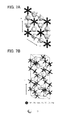
- a wurtzite crystal structure is one of crystal structures which are observed in ionic crystals of cations and anions bound at 1:1.
- FIGS. 6A and 6B illustrate a wurtzite crystal structure; black circles represent gallium or aluminum, and white circles represent oxygen.
- FIG. 6A is a schematic diagram of a wurtzite crystal structure in the a-b plane
- FIG. 6B is a schematic diagram of a wurtzite crystal structure in which the c-axis direction is the vertical direction.
- FIGS. 7A and 7B illustrate a corundum crystal structure; black circles represent indium, gallium, titanium, vanadium, chromium, iron, or aluminum, and white circles represent oxygen.
- FIG. 7A is a schematic diagram of a corundum crystal structure in the a-b plane
- FIG. 7B is a schematic diagram of a corundum crystal structure in which the c-axis direction is the vertical direction.
- the second material film is a crystalline oxide semiconductor film including zinc, indium, or gallium.
- Examples thereof are four-component metal oxides such as an In—Al—Ga—Zn—O-based material and an In—Sn—Ga—Zn—O-based material, three-component metal oxides such as an In—Ga—Zn—O-based material, an In—Al—Zn—O-based material, an In—Sn—Zn—O-based material, and a Sn—Ga—Zn—O-based material, an Al—Ga—Zn—O-based material, and a Sn—Al—Zn—O-based material, two-component metal oxides such as an In—Zn—O-based material, an In—Ga—O-based material, a Sn—Zn—O-based material, and an Al—Zn—O-based material, and the like.
- an In—Si—Ga—Zn—O-based material an In—Ga—B—Zn—O-based material, or an In—B—Zn—O-based material may be used.
- the above materials may contain SiO 2 .
- an In—Ga—Zn—O-based material means an oxide material containing indium (In), gallium (Ga), and zinc (Zn), and there is no limitation on the composition ratio thereof.
- the material may contain an element other than In, Ga, and Zn.
- the second material film is formed by a sputtering method, and the substrate temperature in the film formation is set to be higher than or equal to 200° C. and lower than or equal to 400° C.
- the substrate temperature in the film formation is set to be higher than or equal to 200° C. and lower than or equal to 400° C.
- the temperature of the surface where the film is formed is preferably higher than or equal to 250° C. and lower than or equal to the upper limit of the heat treatment temperature for the substrate.
- the temperature at which entry of impurities such as water or hydrogen into a film to be formed is prevented and the impurity is released to a vapor phase in the chamber is 250° C.
- the upper limit of the temperature of the surface where a film is formed by a sputtering method is the upper limit of the heat treatment temperature for the substrate or the upper limit of the temperature of the film to be formed (if the temperature exceeds the latter upper limit, components in the film significantly change).
- the pressure of a treatment chamber in a sputtering apparatus for forming the second material film is set to 0.4 Pa or less, whereby entry of impurities such as an alkali metal or hydrogen into an object to be formed or a surface of the object to be formed can be suppressed.
- impurities such as an alkali metal or hydrogen
- hydrogen may be contained in the object as a hydrogen molecule, water, a hydroxyl group, or hydride in some cases in addition to a hydrogen atom.
- the leakage rate of the treatment chamber of the sputtering apparatus is set lower than or equal to 1 ⁇ 10 ⁇ 10 Pa ⁇ m 3 /sec, entry of impurities such as an alkali metal and hydride into the crystalline oxide semiconductor film that is being formed by a sputtering method can be suppressed.
- the external leakage refers to inflow of a gas from the outside of a vacuum system through a minute hole, a sealing defect, or the like.
- the internal leakage is due to leakage through a partition, such as a valve, in a vacuum system or due to released gas from an internal member. Measures need to be taken from both aspects of external leakage and internal leakage in order that the leakage rate be lower than or equal to 1 ⁇ 10 ⁇ 10 Pa ⁇ m 3 /sec.
- an open/close portion of the treatment chamber is preferably sealed with a metal gasket.
- a metal material covered with iron fluoride, aluminum oxide, or chromium oxide is preferably used.
- the metal gasket realizes higher adhesion than an O-ring, and can reduce the external leakage. Further, by use of a metal material covered with iron fluoride, aluminum oxide, chromium oxide, or the like which is in the passive state, released gas containing hydrogen generated from the metal gasket is suppressed, so that the internal leakage can also be reduced.
- the above-mentioned member of the sputtering apparatus may be covered with iron fluoride, aluminum oxide, chromium oxide, or the like which is in the passive state.
- the member provided inside the treatment chamber of the sputtering apparatus is preferably formed with only a metal material as much as possible.
- a surface is preferably covered thinly with iron fluoride, aluminum oxide, chromium oxide, or the like which is in the passive state so as to reduce the released gas.
- the length of a pipe between the gas refiner and the treatment chamber is less than or equal to 5 m, preferably less than or equal to 1 m.
- the length of the pipe is less than or equal to 5 m, or less than or equal to 1 m, the effect of the released gas from the pipe can be reduced accordingly.
- a pipe through which a sputtering gas flows from a cylinder to the treatment chamber of the sputtering apparatus is preferably a metal pipe the inside of which is covered with iron fluoride, aluminum oxide, chromium oxide, or the like which is in the passive state.
- the amount of released gas containing hydrogen is small and entry of impurities into the film formation gas can be reduced as compared with a SUS316L-EP pipe, for example.
- a high-performance ultra-compact metal gasket joint (a UPG joint) is preferably used as a joint of the pipe.
- a structure where all the materials of the pipe are metal materials is preferable, because the effect of the generated released gas or the external leakage can be reduced as compared to a structure where a resin or the like is used.
- Evacuation of the treatment chamber of the sputtering apparatus is preferably performed with a rough vacuum pump, such as a dry pump, and a high vacuum pump, such as a sputter ion pump, a turbo molecular pump, or a cryopump, in appropriate combination.
- the turbo molecular pump has an outstanding capability in evacuating a large-sized molecule, whereas it has a low capability in evacuating hydrogen or water.
- combination of a cryopump having a high capability in evacuating water and a sputter ion pump having a high capability in evacuating hydrogen is effective.
- the adsorbate does not affect the pressure in the treatment chamber, but the adsorbate leads to release of gas at the time of the evacuation of the treatment chamber. Therefore, although the leakage rate and the evacuation rate do not have a correlation, it is important that the adsorbate present in the treatment chamber be desorbed as much as possible and evacuation be performed in advance with use of a pump having high evacuation capability.
- the treatment chamber may be subjected to baking for promotion of desorption of the adsorbate. By the baking, the rate of desorption of the adsorbate can be increased about tenfold.
- the baking should be performed at a temperature higher than or equal to 100° C. and lower than or equal to 450° C. At this time, when the adsorbate is removed while an inert gas is introduced, the rate of desorption of water or the like, which is difficult to desorb simply by evacuation, can be further increased.
- an alkali metal, hydrogen atoms, hydrogen molecules, water, a hydroxyl group, hydride, or the like entering the crystalline oxide semiconductor film can be reduced.
- concentration of an alkali metal such as lithium, sodium, or potassium can be reduced in the crystalline oxide semiconductor film.
- a crystalline oxide semiconductor film is formed.
- purification of materials is performed during film formation, and accordingly the crystalline oxide semiconductor film including an extremely small amount of impurities in which the concentration of an alkali metal is lower than or equal to 5 ⁇ 10 16 atoms/cm 3 and the concentration of hydrogen is lower than or equal to 1 ⁇ 10 19 atoms/cm 3 can be formed.
- the thus obtained stack of the first and second material films is used for a transistor, whereby the transistor can have stable electrical characteristics and high reliability. Further, by setting the maximum heating temperature in the process for transistors to be lower than or equal to 450° C., mass production of highly reliable semiconductor devices can be performed with use of a large-sized substrate such as a mother glass.
- an entrapment vacuum pump is preferably used for evacuating the treatment chamber when the first material film and/or the second material film and/or a gate insulating layer are/is manufactured.
- a cryopump, an ion pump, or a titanium sublimation pump is preferably used.
- the above entrapment vacuum pump functions so as to reduce the amount of hydrogen, water, a hydroxyl group, or hydride in the first material film and/or the second material film and/or the gate insulating layer.
- the manufacturing steps of film formation, substrate transfer, and the like are preferably performed in an atmosphere where these impurities are sufficiently reduced.
- a semiconductor device obtained by the above manufacturing method is also one embodiment of the invention.
- the embodiment of the invention is a semiconductor device including a first material film having a hexagonal crystal structure over an insulating surface, a second material film having a hexagonal crystal structure on and in contact with the first material film, a gate insulating layer over the second material film, and a gate electrode layer over the gate insulating layer.
- the second material film is thicker than the first material film, and the second material film is a crystalline oxide semiconductor film.
- Another embodiment of the invention is a semiconductor device including a gate electrode layer over an insulating surface, a gate insulating layer over the gate electrode layer, a first material film having a hexagonal crystal structure over the gate insulating layer, and a second material film having a hexagonal crystal structure on and in contact with the first material film.
- the second material film is thicker than the first material film, and the second material film is a crystalline oxide semiconductor film.
- a transistor in which a channel region is included in a crystalline oxide semiconductor film having a hexagonal crystal structure where bonds for forming hexagonal lattices are formed in the a-b plane and c-axes are substantially perpendicular to a plan surface of a substrate which is substantially parallel to the a-b plane, is manufactured, whereby the amount of change in the threshold voltage of the transistor between before and after performance of a bias-thermal stress (BT) test or light irradiation of the transistor can be reduced.
- BT bias-thermal stress
- a crystalline oxide semiconductor has higher orderliness of a bond between metal and oxygen (-M-O-M-, where O represents an oxygen atom and M represents a metal atom) than an amorphous oxide semiconductor.
- the coordination number may vary depending on the kind of metal.
- the coordination number is substantially uniform. Accordingly, microscopic oxygen vacancies can be reduced, and instability and charge transfer due to attachment or detachment of a hydrogen atom (including a hydrogen ion) or an alkali metal atom in a “space” described later can be reduced.
- Movement of such an atom may cause variation in characteristics of an oxide semiconductor, and thus the existence of such an atom leads to a significant problem in reliability.
- movement of such an atom is caused by application of a high electric field or light energy; therefore, when an oxide semiconductor is used under such a condition, characteristics thereof are unstable. That is, the reliability of an amorphous oxide semiconductor is inferior to that of a crystalline oxide semiconductor.
- Sample 2 that is actually obtained and described below includes a crystalline oxide semiconductor film obtained by forming a first material film at a film formation temperature of 200° C. and then performing heating at 450° C. in a nitrogen atmosphere and by forming a second material film at a film formation temperature of 200° C. and then performing heating at 450° C. in a dry air atmosphere.
- Sample 2 includes the crystalline oxide semiconductor film including the first and second material films of the same material; it is needless to say that the same applies even when the first and second material films include different materials.
- Sample 1 that is used for comparison includes a crystalline oxide semiconductor film obtained by heating a single-layer material film by RTA at 650° C. and then performing heating at 450° C. in a dry air atmosphere.
- an Id ⁇ Vg curve of a transistor is measured, which is obtained by measuring the current (Id) between a drain electrode and a source electrode of the transistor when the voltage (Vg) between a gate electrode and the source electrode of the transistor is changed with the transistor irradiated with light.
- Id current
- Vg voltage
- Vg voltage between a gate electrode and the source electrode of the transistor
- Negative-bias temperature stress photodegradation in Samples 1 and 2 is shown in FIG. 11 .
- the source-drain voltage (Vd) is 0.1 V.
- the source-drain voltage (Vd) is 0.1 V.
- ⁇ 1 and ⁇ 2 depend on the trap density.
- a method for calculating ⁇ 1 and ⁇ 2 is referred to as a photoresponse defect evaluation method.
- FIG. 13 is a schematic diagram of an assumed donor level.
- FIG. 14 shows measurement results in the case where the substrate temperature in formation of an oxide semiconductor film is 400° C. and in the case where the substrate temperature in formation of an oxide semiconductor film is 200° C.
- the peak intensity in the vicinity of about 1.8 eV was much lower than that in the case where the substrate temperature is 200° C.
- the measurement results indicate that the density of the donor level is significantly reduced while the depth thereof is not changed.
- Oxide semiconductor films were formed under varied conditions of the substrate temperature, were compared to each other, and were each evaluated as a single film.
- Sample A has a structure in which a 50-nm-thick oxide semiconductor film is formed over a quartz substrate (thickness: 0.5 mm).
- the distance between the substrate and the target is 170 mm
- the substrate temperature
- FIG. 15A is a graph showing the g-factor of Sample A.
- Sample B is formed in such a manner that deposition is performed under the same conditions as Sample A and then heating is performed at 450° C. for 1 hour in a nitrogen atmosphere.
- FIG. 15B is a graph showing the g-factor of Sample B.
- Sample C is formed in such a manner that deposition is performed under the same conditions as Sample A and then heating is performed at 450° C. for 1 hour in a mixed atmosphere of nitrogen and oxygen.
- FIG. 15C is a graph showing the g-factor of Sample C.
- Samples D, E, F, and G each have a structure in which a 100-nm-thick oxide semiconductor film is formed over a quartz substrate (thickness: 0.5 mm).
- Samples D, E, F, and G are formed at different substrate temperatures: room temperature for Sample D, 200° C. for Sample E, 300° C. for Sample F, and 400° C. for Sample G.
- FIG. 17 is a graph of ESR measurement of Sample B and shows a difference (anisotropy) in the g-factor between the case where a magnetic field is applied perpendicularly to a substrate surface and the case where a magnetic field is applied in parallel to the substrate surface.
- FIG. 18 is a graph of ESR measurement of Sample H which is formed in such a manner that deposition is performed under the same conditions as Sample G and then heating is performed at 450° C. for 1 hour in a nitrogen atmosphere, and shows a difference (anisotropy) in the g-factor between the case where a magnetic field is applied perpendicularly to a substrate surface and the case where a magnetic field is applied in parallel to the substrate surface.
- anisotropy in the g-factor between the case where a magnetic field is applied perpendicularly to a substrate surface and the case where a magnetic field is applied in parallel to the substrate surface.
- ESR measurement was performed under varied conditions of the thickness of an oxide semiconductor film.
- a dangling bond of metal has anisotropy and that the anisotropy is increased as the deposition temperature gets higher because higher crystallinity is obtained at higher deposition temperature.
- the dangling bond of metal exists not at the interface or surface but in the bulk.
- a crystalline oxide semiconductor film can be formed thereover at 450° C. or lower.
- mass production of highly reliable semiconductor devices can be performed with use of a large-sized substrate such as a mother glass.
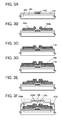
- FIGS. 1A to 1E are cross-sectional views of one embodiment of the present invention.
- FIGS. 2A to 2D are cross-sectional views of one embodiment of the present invention.
- FIGS. 3A to 3F are cross-sectional views of one embodiment of the present invention.
- FIGS. 4A to 4E are cross-sectional views of one embodiment of the present invention.
- FIGS. 5A to 5D are cross-sectional views and a top view of one embodiment of the present invention.
- FIGS. 6A and 6B are schematic diagrams of a wurtzite crystal structure.
- FIGS. 7A and 7B are schematic diagrams of a corundum crystal structure.
- FIG. 8 is a top view illustrating an example of a manufacturing apparatus used to manufacture one embodiment of the present invention.
- FIGS. 9A to 9C are a block diagram and equivalent circuit diagrams of one embodiment of the present invention.
- FIGS. 10A to 10D are external views of electronic devices of one embodiment of the present invention.
- FIG. 11 is a graph for describing negative-bias temperature stress.
- FIGS. 12A and 12B are graphs for describing time dependence of photocurrent.
- FIG. 13 is a schematic diagram showing a donor level.
- FIG. 14 is a graph showing measurement results of low-temperature PL.
- FIGS. 15A to 15C are graphs showing results of ESR measurement.
- FIG. 16 is a graph showing results of ESR measurement.
- FIG. 17 is a graph showing results of ESR measurement.
- FIG. 18 is a graph showing results of ESR measurement
- FIG. 19 is a graph showing results of ESR measurement.
- FIG. 20 is a graph showing the relationship between the total number of spins obtained by ESR measurement and the thickness of an oxide semiconductor layer.
- FIGS. 1A to 1E a structure of a semiconductor device and a manufacturing method thereof will be described with reference to FIGS. 1A to 1E .
- FIG. 1E is a cross-sectional view of a top-gate transistor 120 .
- the transistor 120 includes, over a substrate 100 having an insulating surface, an oxide insulating layer 101 , a stack of semiconductor layers including a channel formation region, a source electrode layer 104 a , a drain electrode layer 104 b , a gate insulating layer 102 , a gate electrode layer 112 , and an insulating film 110 a .
- the source electrode layer 104 a and the drain electrode layer 104 b are provided to cover end portions of the stack of semiconductor layers, and the gate insulating layer 102 covering the source electrode layer 104 a and the drain electrode layer 104 b is in contact with part of the stack of semiconductor layers.
- the gate electrode layer 112 is provided over the part of the stack of semiconductor layers with the gate insulating layer 102 interposed therebetween.
- an insulating film 110 b is provided to cover the insulating film 110 a.
- a process for manufacturing the transistor 120 over the substrate is described below with reference to FIGS. 1A to 1E .
- the oxide insulating layer 101 is formed over the substrate 100 .
- a non-alkali glass substrate formed by a fusion method or a float method, a plastic substrate having heat resistance sufficient to withstand a process temperature of this manufacturing process, or the like can be used.
- a substrate where an insulating film is provided on a surface of a metal substrate such as a stainless steel substrate, or a substrate where an insulating film is provided on a surface of a semiconductor substrate may be used.
- the substrate may have any of the following sizes: the first generation (320 mm ⁇ 400 mm), the second generation (400 mm ⁇ 500 mm), the third generation (550 mm ⁇ 650 mm), the fourth generation (680 mm ⁇ 880 mm or 730 mm ⁇ 920 mm), the fifth generation (1000 mm ⁇ 1200 mm or 1100 mm ⁇ 1250 mm), the sixth generation (1500 mm ⁇ 1800 mm), the seventh generation (1900 mm ⁇ 2200 mm), the eighth generation (2160 mm ⁇ 2460 mm), the ninth generation (2400 mm ⁇ 2800 mm or 2450 mm ⁇ 3050 mm), the tenth generation (2950 mm ⁇ 3400 mm), and the like.
- the preferable heating temperature in the manufacturing process is lower than or equal to 600° C., further preferably, lower than or equal to 450° C.
- the oxide insulating layer 101 is formed by a PCVD method or a sputtering method to have a thickness greater than or equal to 50 nm and less than or equal to 600 nm, using one of a silicon oxide film, a gallium oxide film, an aluminum oxide film, a silicon oxynitride film, an aluminum oxynitride film, and a silicon nitride oxide film or a stacked layer including any of the above films.
- the oxide insulating layer 101 used as a base insulating layer preferably contains a large amount of oxygen which exceeds at least the stoichiometry in (a bulk of) the layer. For example, in the case where a silicon oxide film is used, the composition formula is SiO 2+ ⁇ ( ⁇ >0).
- the oxide insulating layer 101 When the oxide insulating layer 101 has a large thickness, the amount of oxygen released from the oxide insulating layer 101 in heat treatment to be performed later can be increased, and the increase makes it possible to reduce defects at the interface between the oxide insulating layer 101 and an oxide semiconductor film to be formed later.
- a silicon nitride film, an aluminum nitride film, or the like may be formed as a nitride insulating layer between the oxide insulating layer 101 and the substrate 100 , by a PCVD method or a sputtering method in order to prevent entry of an alkali metal. Since an alkali metal such as Li or Na is an impurity, it is preferable to reduce the content of such an alkali metal.
- a first material film 118 having a thickness of 1 nm to 10 nm is formed over the oxide insulating layer 101 (see FIG. 1A ).
- a gallium nitride film having a hexagonal crystal structure is obtained by a molecular beam epitaxy (MBE) method using gallium and plasma-activated nitrogen.
- MBE molecular beam epitaxy
- a gallium nitride film having a hexagonal crystal structure can be formed by a metal organic chemical vapor deposition (MOCVD) method using trimethyl gallium and an ammonium gas as a source gas and using a nitrogen gas or the like as a carrier gas.
- MOCVD metal organic chemical vapor deposition
- the first material film 118 has bonds for forming hexagonal lattices in the a-b plane and includes a gallium nitride crystal having a hexagonal crystal structure in which the c-axis is substantially perpendicular to a plan surface of the substrate which is substantially parallel to the a-b plane.
- the first material film 118 serves as a seed crystal. Note that the seed crystal includes, in the c-axis direction, at least one atomic layer having bonds for forming hexagonal lattices in the a-b plane.
- a second material film i.e., a crystalline oxide semiconductor film 108 including a crystal having a hexagonal crystal structure, is formed thereover without being exposed to the air (see FIG. 1B ).
- the second material film is thicker than the first material film and is, for example, thicker than 10 nm.
- the distance between the substrate and the target is 170 mm
- the substrate temperature is 400° C.
- the pressure is 0.4 Pa
- the direct-current (DC) power is 0.5 kW.
- a rare gas typically, argon
- oxygen or a mixed gas of a rare gas and oxygen
- a high-purity gas from which impurities such as hydrogen, water, a hydroxyl group, and hydride are removed be used as a sputtering gas.
- the pressure of a treatment chamber for forming the second material film is set to 0.4 Pa or less, whereby entry of impurities such as an alkali metal or hydrogen into the surface or inside of the crystalline oxide semiconductor film can be suppressed.
- the leakage rate of the treatment chamber for forming the second material film is set lower than or equal to 1 ⁇ 10 ⁇ 10 Pa ⁇ m 3 /sec, entry of impurities such as an alkali metal, hydrogen, water, a hydroxyl group, or hydride into the crystalline oxide semiconductor film that is being formed by a sputtering method can be suppressed. Further, with the use of an entrapment vacuum pump as an exhaustion system, counter flow of impurities such as an alkali metal, hydrogen, water, a hydroxyl group, or hydride from the exhaustion system can be reduced.
- the concentration of lithium can be 5 ⁇ 10 15 cm ⁇ 3 or less, preferably 1 ⁇ 10 15 cm ⁇ 3 or less; the concentration of sodium can be 5 ⁇ 10 16 cm ⁇ 3 or less, preferably 1 ⁇ 10 16 cm ⁇ 3 or less, more preferably 1 ⁇ 10 15 cm ⁇ 3 or less; and the concentration of potassium can be 5 ⁇ 10 15 cm ⁇ 3 or less, preferably 1 ⁇ 10 15 cm ⁇ 3 or less.
- An alkali metal and an alkaline earth metal are unfavorable impurities for the crystalline oxide semiconductor film and are preferably contained as little as possible.
- sodium is diffused to the oxide insulating film in contact with the crystalline oxide semiconductor and becomes Na + .
- sodium cuts a bond between metal and oxygen or enters the bond in the crystalline oxide semiconductor.
- transistor characteristics deteriorate (e.g., the transistor becomes normally-on (the shift of a threshold voltage to a negative side) or the mobility is decreased).
- this also causes variation in the characteristics.
- Such a problem is significant especially in the case where the concentration of hydrogen in the crystalline oxide semiconductor film is extremely low.
- the concentration of an alkali metal in the above range in the case where the concentration of hydrogen contained in the crystalline oxide semiconductor film is lower than or equal to 5 ⁇ 10 19 cm ⁇ 3 , particularly lower than or equal to 5 ⁇ 10 18 cm ⁇ 3 .
- the substrate is heated with a heater provided in a substrate supporting member to a temperature higher than or equal to 250° C. and lower than or equal to the upper limit of the heat treatment temperature for the substrate. Accordingly, in the film formation, with use of a seed crystal as a nucleus, crystal growth proceeds while atoms deposited on a film formation surface are being oxidized; thus, the crystalline oxide semiconductor film 108 can be manufactured.
- the crystalline oxide semiconductor film is formed under the above conditions, whereby the amount of impurities in the crystalline oxide semiconductor film can be extremely small (the concentration of an alkali metal is lower than or equal to 5 ⁇ 10 16 atoms/cm 3 , and the concentration of hydrogen is lower than or equal to 1 ⁇ 10 19 atoms/cm 3 ).
- the concentration of an alkali metal is lower than or equal to 5 ⁇ 10 16 atoms/cm 3
- the concentration of hydrogen is lower than or equal to 1 ⁇ 10 19 atoms/cm 3 .
- the crystalline oxide semiconductor film 108 described in this embodiment does not have an amorphous structure but a crystalline structure, ideally, a single crystal structure, and comprises an oxide including a crystal in which the c-axis is substantially perpendicular to a plan surface of the substrate (such a crystal is also referred to as C-Axis Aligned Crystal (CAAC)).
- CAAC C-Axis Aligned Crystal
- heat treatment is performed under a condition where the atmosphere of a chamber in which the substrate is set is an atmosphere of nitrogen or dry air.
- the temperature of the heat treatment is higher than or equal to 400° C. and lower than or equal to 750° C.
- heating time of the heat treatment is longer than or equal to 1 minute and shorter than or equal to 24 hours.
- the steps from the formation of the oxide insulating layer 101 to the heat treatment be performed successively without exposure to air.
- a manufacturing apparatus whose top view is illustrated in FIG. 8 may be used.
- the manufacturing apparatus illustrated in FIG. 8 is a single wafer multi-chamber apparatus, which includes three film formation devices 10 a , 10 b , and 10 c , a substrate supply chamber 11 provided with three cassette ports 14 for holding process substrates, load lock chambers 12 a and 12 b , a transfer chamber 13 , a substrate heating chamber 15 , and the like.
- a transfer robot for transferring process substrates is provided in each of the substrate supply chamber 11 and the transfer chamber 13 .
- the atmospheres of the film formation devices 10 a , 10 b , and 10 c , the transfer chamber 13 , and the substrate heating chamber 15 are preferably controlled so as to hardly contain hydrogen and moisture (i.e., to an inert atmosphere, a reduced pressure atmosphere, or a dry air atmosphere).
- a preferable atmosphere is a dry nitrogen atmosphere in which the dew point of moisture is ⁇ 40° C. or lower, preferably ⁇ 50° C. or lower.
- a process substrate is transferred from the substrate supply chamber 11 to the substrate heating chamber 15 through the load lock chamber 12 a and the transfer chamber 13 ; moisture attached to the process substrate is removed by vacuum baking in the substrate heating chamber 15 ; the process substrate is transferred to the film formation device 10 c through the transfer chamber 13 ; and the oxide insulating layer 101 is formed in the film formation device 10 c . Then, the process substrate is transferred to the film formation device 10 a through the transfer chamber 13 without exposure to air, and the first material film 118 having a thickness of 5 nm is formed in the film formation device 10 a .
- the process substrate is transferred to the film formation device 10 b through the transfer chamber 13 , and the crystalline oxide semiconductor film 108 which is thicker than 10 nm is formed in the film formation device 10 b . Then, the process substrate is transferred to the substrate heating chamber 15 through the transfer chamber 13 without exposure to air and the heat treatment is performed. As described above, with use of the manufacturing apparatus illustrated in FIG. 8 , a manufacturing process can proceed without exposure to air.
- the stack of semiconductor layers including the first material film 118 and the crystalline oxide semiconductor film 108 is processed into an island-shaped stack of semiconductor layers.
- the interface between the first material film 118 and the crystalline oxide semiconductor film 108 is indicated by a solid line and these films are described as a stack of layers because they include different materials. In some cases, the interface may become indistinct due to heat treatment or the like in a later step. In the case where the first material film is formed using ⁇ -Ga 2 O 3 or In 2 O 3 , the interface may be indistinct because it partly includes the same material as the crystalline oxide semiconductor film 108 .
- the stack of semiconductor layers can be processed by being etched after a mask having a desired shape is formed over the stack of semiconductor layers.
- the mask may be formed by a method such as photolithography or an ink jet method.
- a conductive film used for forming a source electrode layer and a drain electrode layer (including a wiring formed using the same layer as the source electrode layer and the drain electrode layer) is formed over the stack of semiconductor layers and processed into the source electrode layer 104 a and the drain electrode layer 104 b (see FIG. 1C ).
- the source electrode layer 104 a and the drain electrode layer 104 b can be formed by a sputtering method or the like so as to have a single-layer structure or a stacked-layer structure using any of metal materials such as molybdenum, titanium, tantalum, tungsten, aluminum, copper, neodymium, and scandium or an alloy material containing any of the above metal materials.
- the gate insulating layer 102 is formed to be in contact with part of the stack of semiconductor layers and cover the source electrode layer 104 a and the drain electrode layer 104 b (see FIG. 1D ).
- the gate insulating layer 102 is an oxide insulating layer, which is formed by a plasma CVD method, a sputtering method, or the like to have a single-layer structure or a stacked-layer structure using any of silicon oxide, silicon oxynitride, silicon nitride oxide, aluminum oxide, gallium oxide, aluminum oxynitride, aluminum nitride oxide, and hafnium oxide, and a combination thereof.
- the thickness of the gate insulating layer 102 is greater than or equal to 10 nm and less than or equal to 200 nm.
- a silicon oxide film having a thickness of 100 nm is formed by a sputtering method.
- second heat treatment is performed.
- the second heat treatment is performed in an inert atmosphere, an oxygen atmosphere, or a mixed atmosphere of oxygen and nitrogen at a temperature higher than or equal to 200° C. and lower than or equal to 400° C.
- heating time of the second heat treatment is longer than or equal to 1 minute and shorter than or equal to 24 hours.
- oxygen is supplied from the gate insulating layer 102 to the stack of semiconductor layers. The higher the temperature of heating treatment is, the more suppressed is the amount of change in the threshold voltage at the time of a ⁇ BT test performed with light irradiation.
- a conductive film is formed over the gate insulating layer 102 and subjected to a photolithography step, so that the gate electrode layer 112 is formed.
- the gate electrode layer 112 overlaps with part of the stack of semiconductor layers with the gate insulating layer 102 interposed therebetween.
- the conductive film for forming the gate electrode layer 112 can be formed by a sputtering method or the like to have a single-layer structure or a stacked-layer structure using any of metal materials such as molybdenum, titanium, tantalum, tungsten, aluminum, copper, neodymium, and scandium or an alloy material which contains any of these materials as a main component.
- the insulating film 110 a and the insulating film 110 b are formed to cover the gate electrode layer 112 and the gate insulating layer 102 (see FIG. 1E ).
- the insulating film 110 a and the insulating film 110 b can be formed to have a single-layer structure or a stacked-layer structure using silicon oxide, silicon nitride, gallium oxide, silicon oxynitride, silicon nitride oxide, aluminum oxide, aluminum nitride, aluminum oxynitride, aluminum nitride oxide, hafnium oxide, or a mixed material of these materials.
- a silicon oxide film having a thickness of 300 nm is formed by a sputtering method, and heat treatment is performed for an hour at 250° C. in a nitrogen atmosphere.
- a silicon nitride film is formed by a sputtering method. Since an alkali metal such as Li or Na is an impurity, the content of the alkali metal is preferably reduced.
- the concentration of the alkali metal in the stack of semiconductor layers is lower than or equal to 2 ⁇ 10 16 cm ⁇ 3 , preferably, lower than or equal to 1 ⁇ 10 15 cm ⁇ 3 .
- the transistor 120 has a channel region in the crystalline oxide semiconductor film including a crystal having a hexagonal crystal structure in which bonds for forming hexagonal lattices are formed in the a-b plane and the c-axes are substantially perpendicular to a plan surface of the substrate which is substantially parallel to the a-b plane.
- the transistor 120 has a small amount of change in the threshold voltage between before and after light irradiation or the BT test and thus can have stable electrical characteristics.
- FIGS. 2A to 2D an example of a process which is partially different from that described in Embodiment 1 will be described with reference to FIGS. 2A to 2D .
- the same reference numerals are used for the same parts as those in FIGS. 1A to 1E , and description of the parts with the same reference numerals is omitted here.
- FIG. 2D is a cross-sectional view of a top-gate transistor 130 .
- the transistor 130 includes, over the substrate 100 having an insulating surface, the oxide insulating layer 101 , the source electrode layer 104 a , the drain electrode layer 104 b , the stack of semiconductor layers including a channel formation region, the gate insulating layer 102 , the gate electrode layer 112 , and the insulating film 110 a .
- the stack of semiconductor layers is provided to cover the source electrode layer 104 a and the drain electrode layer 104 b .
- the gate electrode layer 112 is provided over part of the stack of semiconductor layers with the gate insulating layer 102 interposed therebetween.
- the insulating film 110 b is provided to cover the insulating film 110 a.
- a process for manufacturing the transistor 130 over the substrate is described below with reference to FIGS. 2A to 2D .
- the oxide insulating layer 101 is formed over the substrate 100 .
- a conductive film used for forming the source electrode layer and the drain electrode layer (including a wiring formed using the same layer as the source electrode layer and the drain electrode layer) is formed over the oxide insulating layer 101 and processed into the source electrode layer 104 a and the drain electrode layer 104 b.
- the first material film 118 having a thickness of 1 nm to 10 nm is formed over the source electrode layer 104 a and the drain electrode layer 104 b (see FIG. 2A ).
- the crystalline oxide semiconductor film 108 which is thicker than 10 nm is formed over the first material film 118 (see FIG. 2B ).
- heat treatment is performed under a condition where the atmosphere of a chamber in which the substrate is set is an atmosphere of nitrogen or dry air.
- the temperature of the heat treatment is higher than or equal to 400° C. and lower than or equal to 750° C.
- the stack of semiconductor layers including the first material film 118 and the crystalline oxide semiconductor film 108 is processed into an island-shaped stack of semiconductor layers.
- the gate insulating layer 102 is formed over the stack of semiconductor layers (see FIG. 2C ).
- a conductive film is formed over the gate insulating layer 102 and subjected to a photolithography step, so that the gate electrode layer 112 is formed.
- the gate electrode layer 112 overlaps with part of the stack of semiconductor layers with the gate insulating layer 102 interposed therebetween.
- the insulating film 110 a and the insulating film 110 b are formed to cover the gate electrode layer 112 and the gate insulating layer 102 (see FIG. 2D ).
- the top-gate transistor 130 is formed.
- the transistor 130 illustrated in FIG. 2D also has a channel region in the crystalline oxide semiconductor film including a crystal having a hexagonal crystal structure in which bonds for forming hexagonal lattices are formed in the a-b plane and the c-axes are substantially perpendicular to a plan surface of the substrate which is substantially parallel to the a-b plane.
- the transistor 130 has a small amount of change in the threshold voltage between before and after light irradiation or the BT test and thus can have stable electrical characteristics.
- Embodiment 1 can be freely combined with Embodiment 1.
- FIGS. 3A to 3F an example of a process which is partially different from that described in Embodiment 1 will be described with reference to FIGS. 3A to 3F .
- the same reference numerals are used for the same parts as those in FIGS. 1A to 1E , and description of the parts with the same reference numerals is omitted here.
- FIG. 3F is a cross-sectional view of a bottom-gate transistor 140 .
- the transistor 140 includes, over the substrate 100 having an insulating surface, the oxide insulating layer 101 , the gate electrode layer 112 , the gate insulating layer 102 , the source electrode layer 104 a , the drain electrode layer 104 b , the stack of semiconductor layers including a channel formation region, and the insulating film 110 a .
- the stack of semiconductor layers is provided to cover the source electrode layer 104 a and the drain electrode layer 104 b .
- a region functioning as a channel formation region is part of the stack of semiconductor layers overlapping with the gate electrode layer 112 with the gate insulating layer 102 interposed therebetween.
- the insulating film 110 b is provided to cover the insulating film 110 a.
- a process for manufacturing the transistor 140 over the substrate is described below with reference to FIGS. 3A to 3F .
- the oxide insulating layer 101 is formed over the substrate 100 .
- a conductive film is formed over the oxide insulating layer 101 and subjected to a photolithography step, so that the gate electrode layer 112 is formed.
- the gate insulating layer 102 is formed over the gate electrode layer 112 (see FIG. 3A ).
- a conductive film for forming the source electrode layer and the drain electrode layer (including a wiring formed using the same layer as the source electrode layer and the drain electrode layer) is formed over the gate insulating layer 102 and processed into the source electrode layer 104 a and the drain electrode layer 104 b (see FIG. 3B ).
- the first material film 118 having a thickness of 1 nm to 10 nm is formed over the source electrode layer 104 a and the drain electrode layer 104 b (see FIG. 3C ).
- the crystalline oxide semiconductor film 108 which is thicker than 10 nm is formed over the first material film 118 (see FIG. 3D ).
- heat treatment is performed under a condition where the atmosphere of a chamber in which the substrate is set is an atmosphere of nitrogen or dry air.
- the temperature of the heat treatment is higher than or equal to 400° C. and lower than or equal to 750° C.
- heating time of the heat treatment is longer than or equal to 1 minute and shorter than or equal to 24 hours.
- the stack of semiconductor layers including the first material film 118 and the crystalline oxide semiconductor film 108 is processed into an island-shaped stack of semiconductor layers (see FIG. 3E ).
- the stack of semiconductor layers can be processed by being etched after a mask having a desired shape is formed over the stack of semiconductor layers.
- the mask may be formed by a method such as photolithography or an ink jet method.
- the insulating film 110 a and the insulating film 110 b are formed to cover the stack of semiconductor layers, the source electrode layer 104 a , and the drain electrode layer 104 b (see FIG. 3F ).
- the bottom-gate transistor 140 is formed.
- the transistor 140 illustrated in FIG. 3F also has a channel region in the crystalline oxide semiconductor film including a crystal having a hexagonal crystal structure in which bonds for forming hexagonal lattices are formed in the a-b plane and the c-axes are substantially perpendicular to a plan surface of the substrate which is substantially parallel to the a-b plane.
- the transistor 140 has a small amount of change in the threshold voltage between before and after light irradiation or the BT test and thus can have stable electrical characteristics.
- Embodiment 1 can be freely combined with Embodiment 1.
- FIGS. 4A to 4E an example of a process which is partially different from that described in Embodiment 3 will be described with reference to FIGS. 4A to 4E .
- the same reference numerals are used for the same parts as those in FIGS. 3A to 3F , and description of the parts with the same reference numerals is omitted here.
- FIG. 4E is a cross-sectional view of a bottom-gate transistor 150 .
- the transistor 150 includes, over the substrate 100 having an insulating surface, the oxide insulating layer 101 , the gate electrode layer 112 , the gate insulating layer 102 , the stack of semiconductor layers including a channel formation region, the source electrode layer 104 a , the drain electrode layer 104 b , and the insulating film 110 a .
- the source electrode layer 104 a and the drain electrode layer 104 b are provided to cover the stack of semiconductor layers.
- a region functioning as a channel formation region is part of the stack of semiconductor layers overlapping with the gate electrode layer 112 with the gate insulating layer 102 interposed therebetween.
- the insulating film 110 b is provided to cover the insulating film 110 a.
- a process for manufacturing the transistor 150 over the substrate is described below with reference to FIGS. 4A to 4E .
- the oxide insulating layer 101 is formed over the substrate 100 .
- a conductive film is formed over the oxide insulating layer 101 and subjected to a photolithography step, so that the gate electrode layer 112 is formed.
- the gate insulating layer 102 is formed over the gate electrode layer 112 (see FIG. 4A ).
- the first material film 118 having a thickness of 1 nm to 10 nm is formed over the gate insulating layer 102 (see FIG. 4B ).
- the crystalline oxide semiconductor film 108 which is thicker than 10 nm is formed over the first material film 118 (see FIG. 4C ).
- the stack of semiconductor layers including the first material film 118 and the crystalline oxide semiconductor film 108 is processed into an island-shaped stack of semiconductor layers (see FIG. 4D ).
- the stack of semiconductor layers can be processed by being etched after a mask having a desired shape is formed over the stack of semiconductor layers.
- the mask may be formed by a method such as photolithography or an ink jet method.
- a conductive film used for forming the source electrode layer and the drain electrode layer (including a wiring formed using the same layer as the source electrode layer and the drain electrode layer) is formed over the stack of semiconductor layers and processed into the source electrode layer 104 a and the drain electrode layer 104 b.
- the insulating film 110 a and the insulating film 110 b are formed to cover the stack of semiconductor layers, the source electrode layer 104 a , and the drain electrode layer 104 b (see FIG. 4E ).
- the insulating film 110 a is preferably formed using an oxide insulating material and subjected to heat treatment after film formation.
- oxygen is supplied from the insulating film 110 a to the stack of semiconductor layers.
- the heat treatment is performed in an inert atmosphere, an oxygen atmosphere, or a mixed atmosphere of oxygen and nitrogen at a temperature higher than or equal to 200° C. and lower than or equal to 400° C.
- heating time of this heat treatment is longer than or equal to 1 minute and shorter than or equal to 24 hours.
- the bottom-gate transistor 150 is formed.
- the transistor 150 illustrated in FIG. 4E also has a channel region in the crystalline oxide semiconductor film including a crystal having a hexagonal crystal structure in which bonds for forming hexagonal lattices are formed in the a-b plane and the c-axes are substantially perpendicular to a plan surface of the substrate which is substantially parallel to the a-b plane.
- the transistor 150 has a small amount of change in the threshold voltage between before and after light irradiation or the BT test and thus can have stable electrical characteristics.
- Embodiment 1 can be freely combined with Embodiment 1.
- FIGS. 5A to 5D an example of a structure which is partially different from that described in Embodiment 1 will be described with reference to FIGS. 5A to 5D .
- the same reference numerals are used for the same parts as those in FIGS. 1A to 1E , and description of the parts with the same reference numerals is omitted here.
- Embodiment 1 the example of using a gallium nitride film as the first material film is described; in this embodiment, an example of using another material having a hexagonal crystal structure is described below.
- the aluminum nitride film does not function as a semiconductor layer but functions as part of a base insulating layer because it is an insulating material.
- An ⁇ -Al 2 O 3 film which has a corundum crystal structure can also be used.
- the ⁇ -Al 2 O 3 film can be formed by a chemical vapor deposition method.
- the ⁇ -Al 2 O 3 film also does not function as a semiconductor layer but functions as part of a base insulating layer because it is an insulating material.
- FIG. 5C illustrates a cross-sectional structure of a top-gate transistor 160 and is a cross-sectional view along a dashed line C 1 -C 2 in FIG. 5D which is a top view.
- the transistor 160 includes, over the substrate 100 having an insulating surface, the oxide insulating layer 101 , the first material film 118 , the crystalline oxide semiconductor film 108 including a channel formation region, n + layers 113 a and 113 b , the source electrode layer 104 a , the drain electrode layer 104 b , the gate insulating layer 102 , the gate electrode layer 112 , an insulating layer 114 , and the insulating film 110 a .
- the source electrode layer 104 a and the drain electrode layer 104 b are provided to cover end portions of the crystalline oxide semiconductor film 108 and end portions of the n + layers 113 a and 113 b .
- the gate insulating layer 102 covering the source electrode layer 104 a and the drain electrode layer 104 b is in contact with part of the crystalline oxide semiconductor film 108 .
- the gate electrode layer 112 is provided over the part of the crystalline oxide semiconductor film 108 with the gate insulating layer 102 interposed therebetween.
- the insulating layer 114 overlapping with the source electrode layer 104 a and the drain electrode layer 104 b is provided over the gate insulating layer 102 in order to reduce parasitic capacitance generated between the gate electrode layer 112 and the source electrode layer 104 a and parasitic capacitance generated between the gate electrode layer 112 and the drain electrode layer 104 b . Further, the gate electrode layer 112 and the insulating layer 114 are covered with the insulating film 110 a , and the insulating film 110 b is provided to cover the insulating film 110 a.
- a process for manufacturing the transistor 160 over the substrate is described below with reference to FIGS. 5A to 5C .
- the oxide insulating layer 101 is formed over the substrate 100 .
- the oxide insulating layer 101 is formed using a silicon oxide film, a gallium oxide film, an aluminum oxide film, a silicon oxynitride film, an aluminum oxynitride film, or a silicon nitride oxide film.
- the first material film 118 having a thickness of 1 nm to 10 nm is formed over the oxide insulating layer 101 (see FIG. 5A ).
- a quartz substrate is used as the substrate, and an aluminum nitride film formed by a sublimation method is used as the first material film 118 .
- the crystalline oxide semiconductor film 108 which is thicker than 10 nm is formed over the first material film 118 (see FIG. 5B ).
- the distance between the substrate and the target is 170 mm
- the substrate temperature is 400° C.
- the pressure is 0.4 Pa
- the direct-current (DC) power is 0.5 kW.
- heat treatment is performed under a condition where the atmosphere of a chamber in which the substrate is set is an atmosphere of nitrogen or dry air.
- the temperature of the heat treatment is higher than or equal to 400° C. and lower than or equal to 650° C.
- heating time of the heat treatment is longer than or equal to 1 minute and shorter than or equal to 24 hours.
- a film functioning as an n + layer and having a thickness of 1 nm to 10 nm is formed using an In—Zn—O-based material, an In—Sn—O-based material, an In—O-based material, or a Sn—O-based material.
- SiO 2 may be contained in the above material for the n + layer.
- an In—Sn—O film containing SiO 2 is formed to a thickness of 5 nm.
- the first material film 118 the crystalline oxide semiconductor film 108 , and the film functioning as an n + layer are processed.
- a conductive film used for forming the source electrode layer and the drain electrode layer (including a wiring formed using the same layer as the source electrode layer and the drain electrode layer) is formed over the film functioning as an n + layer and processed into the source electrode layer 104 a and the drain electrode layer 104 b .
- Etching is performed when the conductive film is processed or after the conductive film is processed.
- the film functioning as an n + layer is selectively etched, whereby the crystalline oxide semiconductor film 108 is partly exposed. Note that selective etching of the film functioning as an n + layer enables formation of the n + layer 113 a which overlaps with the source electrode layer 104 a and the n + layer 113 b which overlaps with the drain electrode layer 104 b . End portions of the n + layers 113 a and 113 b preferably have a tapered shape.
- the source electrode layer 104 a and the drain electrode layer 104 b can be formed by a sputtering method or the like to have a single-layer structure or a stacked-layer structure using any of metal materials such as molybdenum, titanium, tantalum, tungsten, aluminum, copper, neodymium, and scandium or an alloy material containing any of the above metal materials.
- metal materials such as molybdenum, titanium, tantalum, tungsten, aluminum, copper, neodymium, and scandium or an alloy material containing any of the above metal materials.
- the contact resistance can be lower than the contact resistance in the case where the crystalline oxide semiconductor film 108 is in contact with the source electrode layer 104 a or the drain electrode layer 104 b .
- the parasitic capacitance can be reduced, and the amount of change in on-state current (Ion deterioration) by application of a negative gate stress in a BT test can be suppressed.
- the gate insulating layer 102 is formed to be in contact with the exposed part of the crystalline oxide semiconductor film 108 and cover the source electrode layer 104 a and the drain electrode layer 104 b .
- the gate insulating layer 102 is preferably formed using an oxide insulating material and subjected to heat treatment after film formation. By this heat treatment, oxygen is supplied from the gate insulating layer 102 to the crystalline oxide semiconductor film 108 .
- the heat treatment is performed in an inert atmosphere, an oxygen atmosphere, or a mixed atmosphere of oxygen and nitrogen at a temperature higher than or equal to 200° C. and lower than or equal to 400° C. In addition, heating time of the heat treatment is longer than or equal to 1 minute and shorter than or equal to 24 hours.
- an insulating film is formed over the gate insulating layer 102 , and part of the insulating film, overlapping with a region where the gate insulating layer 102 is in contact with the crystalline oxide semiconductor film 108 , is selectively removed, so that part of the gate insulating layer 102 is exposed.
- the insulating layer 114 functions to reduce the parasitic capacitance generated between the source electrode layer 104 a and the gate electrode layer 112 formed later or the parasitic capacitance generated between the drain electrode layer 104 b and the gate electrode layer 112 formed later.
- the insulating layer 114 can be formed using silicon oxide, silicon nitride, aluminum oxide, gallium oxide, a mixed material thereof, or the like.
- the gate electrode layer 112 can be formed by a sputtering method or the like to have a single-layer structure or a stacked-layer structure using any of metal materials such as molybdenum, titanium, tantalum, tungsten, aluminum, copper, neodymium, and scandium or an alloy material which contains any of these materials as a main component.
- the insulating film 110 a and the insulating film 110 b are formed to cover the gate electrode layer 112 and the insulating layer 114 (see FIG. 5C ).
- the insulating film 110 a and the insulating film 110 b can be formed to have a single-layer structure or a stacked-layer structure using any of silicon oxide, silicon nitride, gallium oxide, silicon oxynitride, silicon nitride oxide, aluminum oxide, aluminum nitride, aluminum oxynitride, aluminum nitride oxide, and hafnium oxide or a mixed material of these.
- the top-gate transistor 160 is formed.
- the transistor 160 illustrated in FIG. 5C also has a channel region in the crystalline oxide semiconductor film including a crystal having a hexagonal crystal structure in which bonds for forming hexagonal lattices are formed in the a-b plane and the c-axes are substantially perpendicular to a plan surface of the substrate which is substantially parallel to the a-b plane.
- the transistor 160 has a small amount of change in the threshold voltage between before and after light irradiation or the BT test and thus can have stable electrical characteristics.
- This embodiment can be freely combined with any one of Embodiments 1 to 4.
- the first material film does not function as a semiconductor layer but functions as part of the gate insulating layer.
- the transistor to be disposed in the pixel portion is formed according to any one of Embodiments 1 to 5. Further, the transistor described in any of Embodiments 1 to 5 is an n-channel TFT, and thus a part of a driver circuit that can be formed with n-channel TFTs among driver circuits is formed over the same substrate as the transistor of the pixel portion.
- FIG. 9A is an example of a block diagram of an active matrix display device.
- a pixel portion 5301 Over a substrate 5300 in the display device, a pixel portion 5301 , a first scan line driver circuit 5302 , a second scan line driver circuit 5303 , and a signal line driver circuit 5304 are provided.
- a plurality of signal lines extended from the signal line driver circuit 5304 is arranged and a plurality of scan lines extended from the first scan line driver circuit 5302 and the second scan line driver circuit 5303 is arranged.
- pixels which include display elements are provided in a matrix in respective regions where the scan lines and the signal lines intersect with each other.
- the substrate 5300 in the display device is connected to a timing control circuit (also referred to as a controller or a controller IC) through a connection portion such as a flexible printed circuit (FPC).
- a timing control circuit also referred to as a controller or a controller IC
- FPC flexible printed circuit
- the first scan line driver circuit 5302 , the second scan line driver circuit 5303 , and the signal line driver circuit 5304 are formed over the same substrate 5300 as the pixel portion 5301 . Accordingly, the number of components such as a drive circuit which are provided outside are reduced, so that reduction in cost can be achieved. Further, if the driver circuit is provided outside the substrate 5300 , a wiring would need to be extended and the number of wiring connections would be increased, but if the driver circuit is provided over the substrate 5300 , the number of wiring connections can be reduced. Consequently, improvement in reliability and yield can be achieved.
- FIG. 9B illustrates an example of a circuit configuration of the pixel portion.
- a pixel configuration of a VA liquid crystal display panel is described.
- a plurality of pixel electrode layers is provided in one pixel, and the pixel electrode layers are connected to respective transistors.
- the TFTs are constructed so as to be driven with different gate signals. In other words, signals applied to individual pixel electrode layers in a multi-domain pixel are controlled independently.
- a gate wiring 602 of a transistor 628 and a gate wiring 603 of a transistor 629 are separated so that different gate signals can be given thereto.
- a source or drain electrode layer 616 functioning as a data line is shared by the transistors 628 and 629 .
- any of the transistors described in Embodiments 1 to 5 can be used as appropriate.
- a first pixel electrode layer and a second pixel electrode layer which are each electrically connected to the transistor 628 or the transistor 629 have different shapes and are separated by a slit.
- the second pixel electrode layer is provided so as to surround the external side of the first pixel electrode layer which is spread in a V shape.
- Timing of voltage application is made to vary between the first and second pixel electrode layers by the transistors 628 and 629 in order to control alignment of the liquid crystal.
- the transistor 628 is connected to the gate wiring 602
- the transistor 629 is connected to the gate wiring 603 . When different gate signals are supplied to the gate wiring 602 and the gate wiring 603 , operation timings of the transistor 628 and the transistor 629 can be varied.
- a storage capacitor is formed using a capacitor wiring 690 , a gate insulating layer functioning as a dielectric, and a capacitor electrode electrically connected to the first pixel electrode layer or the second pixel electrode layer.
- the first pixel electrode layer, a liquid crystal layer, and a counter electrode layer overlap with each other to form a first liquid crystal element 651 .
- the second pixel electrode layer, a liquid crystal layer, and a counter electrode layer overlap with each other to form a second liquid crystal element 652 .
- the pixel structure is a multi-domain structure in which the first liquid crystal element 651 and the second liquid crystal element 652 are provided in one pixel.
- the pixel structure is not limited to the structure shown in FIG. 9B .
- a switch, a resistor, a capacitor, a transistor, a sensor, a logic circuit, or the like may be added to the pixel illustrated in FIG. 9B .
- FIG. 9C illustrates another example of a circuit configuration of the pixel portion.
- a pixel structure of a display panel using an organic EL element is described.
- an organic EL element by application of voltage to a light-emitting element, electrons and holes are separately injected from a pair of electrodes into a layer containing a light-emitting organic compound, and current flows.
- the carriers (electrons and holes) are recombined, and thus, the light-emitting organic compound is excited.
- the light-emitting organic compound returns to a ground state from the excited state, thereby emitting light. Owing to such a mechanism, this light-emitting element is referred to as a current-excitation light-emitting element.
- FIG. 9C illustrates an example of a pixel configuration to which digital time grayscale driving can be applied as an example of the semiconductor device.
- one pixel includes two n-channel transistors each of which includes an oxide semiconductor layer as a channel formation region.
- a pixel 6400 includes a switching transistor 6401 , a driving transistor 6402 , a light-emitting element 6404 , and a capacitor 6403 .
- a gate electrode layer of the switching transistor 6401 is connected to a scan line 6406
- a first electrode (one of a source electrode layer and a drain electrode layer) of the switching transistor 6401 is connected to a signal line 6405
- a second electrode (the other of the source electrode layer and the drain electrode layer) of the switching transistor 6401 is connected to a gate electrode layer of the driving transistor 6402 .
- the gate electrode layer of the driving transistor 6402 is connected to a power supply line 6407 through the capacitor 6403 , a first electrode of the driving transistor 6402 is connected to the power supply line 6407 , and a second electrode of the driving transistor 6402 is connected to a first electrode (a pixel electrode) of the light-emitting element 6404 .
- a second electrode of the light-emitting element 6404 corresponds to a common electrode 6408 .
- the common electrode 6408 is electrically connected to a common potential line provided over the same substrate.
- the second electrode (the common electrode 6408 ) of the light-emitting element 6404 is set to a low power supply potential.
- the low power supply potential is a potential that is lower than a high power supply potential with reference to the high power supply potential that is set to the power supply line 6407 .
- GND, 0 V, or the like may be employed, for example.
- a potential difference between the high power supply potential and the low power supply potential is applied to the light-emitting element 6404 and current is supplied to the light-emitting element 6404 , so that the light-emitting element 6404 emits light.
- each potential is set so that the potential difference between the high power supply potential and the low power supply potential is higher than or equal to a forward threshold voltage of the light-emitting element 6404 .
- gate capacitance of the driving transistor 6402 may be used as a substitute for the capacitor 6403 , so that the capacitor 6403 can be omitted.
- the gate capacitance of the driving transistor 6402 may be formed between the channel formation region and the gate electrode layer.
- a video signal is input to the gate electrode layer of the driving transistor 6402 so that the driving transistor 6402 is in either of two states of being sufficiently turned on and turned off. That is, the driving transistor 6402 operates in a linear region.
- a voltage higher than the voltage of the power supply line 6407 is applied to the gate electrode layer of the driving transistor 6402 .
- a voltage higher than or equal to is applied to the signal line 6405 .
- the same pixel configuration as FIG. 9C can be employed by inputting signals in a different way.
- a voltage greater than or equal to the sum of the forward voltage of the light-emitting element 6404 and Vth of the driving transistor 6402 is applied to the gate electrode layer of the driving transistor 6402 .
- the forward voltage of the light-emitting element 6404 indicates a voltage at which a desired luminance is obtained, and includes at least forward threshold voltage.
- the video signal by which the driving transistor 6402 operates in a saturation region is input, so that current can be supplied to the light-emitting element 6404 .
- the potential of the power supply line 6407 is set higher than the gate potential of the driving transistor 6402 .
- the pixel configuration is not limited to that illustrated in FIG. 9C .
- a switch, a resistor, a capacitor, a sensor, a transistor, a logic circuit, or the like may be added to the pixel illustrated in FIG. 9C .
- a semiconductor device disclosed in this specification can be applied to a variety of electronic devices (including game machines).
- electronic devices are a television set (also referred to as a television or a television receiver), a monitor of a computer or the like, a camera such as a digital camera or a digital video camera, a digital photo frame, a mobile phone handset (also referred to as a mobile phone or a mobile phone device), a portable game machine, a portable information terminal, an audio reproducing device, a large-sized game machine such as a pachinko machine, and the like.
- Examples of electronic devices each including the display device described in the above embodiment will be described.
- FIG. 10A illustrates a portable information terminal, which includes a main body 3001 , a housing 3002 , display portions 3003 a and 3003 b , and the like.
- the display portion 3003 b functions as a touch panel. By touching a keyboard 3004 displayed on the display portion 3003 b , a screen can be operated and text can be input.
- the display portion 3003 a may function as a touch panel.
- a liquid crystal panel or an organic light-emitting panel is manufactured by using the transistor described in Embodiment 1 as a switching element and applied to the display portion 3003 a or 3003 b , whereby a highly reliable portable information terminal can be provided.
- the portable information terminal in FIG. 10A can have a function of displaying a variety of information (e.g., a still image, a moving image, and a text image) on the display portion, a function of displaying a calendar, a date, the time, or the like on the display portion, a function of operating or editing information displayed on the display portion, a function of controlling processing by various kinds of software (programs), and the like.
- an external connection terminal e.g., an earphone terminal, a USB terminal, or the like
- a recording media insertion portion, or the like may be provided on a rear surface or a side surface of the housing.
- the portable information terminal illustrated in FIG. 10A may be configured to be able to transmit and receive data wirelessly.
- the portable information terminal can have a structure where desired book data or the like are wirelessly purchased and downloaded from an electronic book server.
- FIG. 10B illustrates a portable music player, which includes, in a main body 3021 , a display portion 3023 , a fixing portion 3022 with which the portable music player can be worn on the ear, a speaker, an operation button 3024 , an external memory slot 3025 , and the like.
- a liquid crystal panel or an organic light-emitting panel is manufactured by using the transistor described in Embodiment 1 as a switching element and applied to the display portion 3023 , whereby a highly reliable portable music player can be provided.
- the portable music player illustrated in FIG. 10B has an antenna, a microphone function, or a wireless communication function and is used with a mobile phone, a user can talk on the phone wirelessly and hands-free while driving a car or the like.
- FIG. 10C illustrates a mobile phone, which includes two housings, a housing 2800 and a housing 2801 .
- the housing 2801 includes a display panel 2802 , a speaker 2803 , a microphone 2804 , a pointing device 2806 , a camera lens 2807 , an external connection terminal 2808 , and the like.
- the housing 2800 includes a solar cell 2810 having a function of charge of the portable information terminal, an external memory slot 2811 , and the like.
- an antenna is incorporated in the housing 2801 .
- the transistor described in Embodiment 1 is applied to the display panel 2802 , whereby a highly reliable mobile phone can be provided.
- the display panel 2802 includes a touch panel.
- a plurality of operation keys 2805 which are displayed as images are indicated by dashed lines in FIG. 10C .
- a power transistor used for a power supply circuit such as a boosting circuit can also be formed when the crystalline oxide semiconductor film 108 of the transistor 120 described in Embodiment 1 has a thickness of 2 ⁇ m to 50 ⁇ m.
- the display panel 2802 changes the orientation of display as appropriate in accordance with the application mode.
- the camera lens 2807 is provided on the same side as the display panel 2802 , so that the mobile phone can be used as a video phone.
- the speaker 2803 and the microphone 2804 can be used for videophone calls, recording, and playing sound, etc. as well as voice calls.
- the housings 2800 and 2801 in a state where they are developed as illustrated in FIG. 10C can be slid so that one is lapped over the other. Therefore, the size of the mobile phone can be reduced, which makes the mobile phone suitable for being carried around.
- the external connection terminal 2808 can be connected to an AC adaptor and a variety of cables such as a USB cable, and charging and data communication with a personal computer or the like are possible. Moreover, the mobile phone can store and transfer a larger amount of data by inserting a recording medium into the external memory slot 2811 .
- an infrared communication function may be provided.
- FIG. 10D illustrates an example of a television set.
- a display portion 9603 is incorporated in a housing 9601 .
- the display portion 9603 can display images.
- the housing 9601 is supported on a stand 9605 incorporating a CPU.
- the transistor described in Embodiment 1 is applied to the display portion 9603 , the television set 9600 with high reliability can be obtained.
- the television set 9600 can be operated with an operation switch of the housing 9601 or a separate remote controller. Further, the remote controller may be provided with a display portion for displaying data output from the remote controller.
- the television set 9600 is provided with a receiver, a modem, and the like. With the use of the receiver, the television set 9600 can receive general television broadcasting. Moreover, when the television set is connected to a communication network with or without wires via the modem, one-way (from a sender to a receiver) or two-way (between a sender and a receiver or between receivers) information communication can be performed.
- the television set 9600 is provided with an external connection terminal 9604 , a storage medium recording and reproducing portion 9602 , and an external memory slot.
- the external connection terminal 9604 can be connected to various types of cables such as a USB cable, and data communication with a personal computer is possible.
- a disk storage medium is inserted into the storage medium recording and reproducing portion 9602 , and reading data stored in the storage medium and writing data to the storage medium can be performed.
- a picture, a video, or the like stored as data in an external memory 9606 inserted to the external memory slot can be displayed on the display portion 9603 .
Abstract
Description
- 1. Field of the Invention
- An embodiment of the present invention relates to a semiconductor device including an oxide semiconductor and a method for manufacturing the semiconductor device.
- In this specification, a semiconductor device generally means a device which can function by utilizing semiconductor characteristics, and an electro-optical device, a semiconductor circuit, and an electronic device are all semiconductor devices.
- 2. Description of the Related Art
- In recent years, a technique for forming a thin film transistor (TFT) using a semiconductor thin film (having a thickness of about several tens of nanometers to several hundred nanometers) formed over a substrate having an insulating surface has attracted attention. Thin film transistors are applied to a wide range of electronic devices such as ICs or electro-optical devices, and thin film transistors that are used as switching elements in image display devices are particularly being developed urgently. There are various kinds of metal oxides, which are used for a wide range of applications.
- Some metal oxides have semiconductor characteristics. Examples of such metal oxides having semiconductor characteristics include tungsten oxide, tin oxide, indium oxide, and zinc oxide. Thin film transistors in each of which such a metal oxide having semiconductor characteristics is used for a channel formation region have already been known (
Patent Documents 1 and 2). - As for an oxide semiconductor used in such a transistor, there is description as follows: an oxide semiconductor is insensitive to impurities; there is no problem when a considerable amount of metal impurities is contained in the film; and soda-lime glass which contains a large amount of alkali metal such as sodium and is inexpensive can also be used (see Non-Patent Document 1).
-
- [Patent Document 1] Japanese Published Patent Application No. 2007-123861
- [Patent Document 2] Japanese Published Patent Application No. 2007-96055
- [Non-Patent Document 1] Kamiya, Nomura, and Hosono, “Carrier Transport Properties and Electronic Structures of Amorphous Oxide Semiconductors: The present status”, KOTAI BUTSURI (SOLID STATE PHYSICS), 2009, Vol. 44, pp. 621-633
- When hydrogen or water, which forms an electron donor, enters an oxide semiconductor in a process for manufacturing a device, the electrical conductivity of the oxide semiconductor may change. Such a phenomenon becomes a factor of change in the electrical characteristics of a transistor including an oxide semiconductor.
- Further, the electrical characteristics of a semiconductor device including an oxide semiconductor may change by irradiation with visible light or ultraviolet light.
- In view of the above problems, one object is to provide a semiconductor device including an oxide semiconductor film, which has stable electrical characteristics and high reliability.
- Another object is to provide a manufacturing process of a semiconductor device, which realizes mass production of highly reliable semiconductor devices by using a large-sized substrate such as a mother glass.
- One embodiment of the disclosed invention is a method for manufacturing a semiconductor device, including the steps of forming a first material film (a film having a hexagonal crystal structure) over an insulating surface and forming a second material film having a hexagonal crystal structure (a crystalline oxide semiconductor film) using the first material film as a nucleus, thereby forming a stack of the first material film and the second material film. Note that the first material film and the second material film are formed using different materials.
- Specifically, as the first material film, a material film having a wurtzite crystal structure (e.g., gallium nitride or aluminum nitride) or a material film having a corundum crystal structure (α-Al2O3, α-Ga2O3, In2O3, Ti2O3, V2O3, Cr2O3, or α-Fe2O3) can be used. In order to obtain a favorable crystal structure, a stack of these material films may be used; for example, a stack of an aluminum nitride film and a gallium nitride film thereover may be used.
- Note that a wurtzite crystal structure is one of crystal structures which are observed in ionic crystals of cations and anions bound at 1:1.
FIGS. 6A and 6B illustrate a wurtzite crystal structure; black circles represent gallium or aluminum, and white circles represent oxygen.FIG. 6A is a schematic diagram of a wurtzite crystal structure in the a-b plane, andFIG. 6B is a schematic diagram of a wurtzite crystal structure in which the c-axis direction is the vertical direction. -
FIGS. 7A and 7B illustrate a corundum crystal structure; black circles represent indium, gallium, titanium, vanadium, chromium, iron, or aluminum, and white circles represent oxygen.FIG. 7A is a schematic diagram of a corundum crystal structure in the a-b plane, andFIG. 7B is a schematic diagram of a corundum crystal structure in which the c-axis direction is the vertical direction. - The second material film is a crystalline oxide semiconductor film including zinc, indium, or gallium. Examples thereof are four-component metal oxides such as an In—Al—Ga—Zn—O-based material and an In—Sn—Ga—Zn—O-based material, three-component metal oxides such as an In—Ga—Zn—O-based material, an In—Al—Zn—O-based material, an In—Sn—Zn—O-based material, and a Sn—Ga—Zn—O-based material, an Al—Ga—Zn—O-based material, and a Sn—Al—Zn—O-based material, two-component metal oxides such as an In—Zn—O-based material, an In—Ga—O-based material, a Sn—Zn—O-based material, and an Al—Zn—O-based material, and the like. In addition, an In—Si—Ga—Zn—O-based material, an In—Ga—B—Zn—O-based material, or an In—B—Zn—O-based material may be used. In addition, the above materials may contain SiO2. For example, an In—Ga—Zn—O-based material means an oxide material containing indium (In), gallium (Ga), and zinc (Zn), and there is no limitation on the composition ratio thereof. In addition, the material may contain an element other than In, Ga, and Zn.
- The second material film is formed by a sputtering method, and the substrate temperature in the film formation is set to be higher than or equal to 200° C. and lower than or equal to 400° C. By setting the substrate temperature in the film formation to be higher than or equal to 200° C. and lower than or equal to 400° C., the second material film formed on and in contact with the surface of the first material film can have a hexagonal crystal structure.
- During formation of the second material film by a sputtering method, the temperature of the surface where the film is formed is preferably higher than or equal to 250° C. and lower than or equal to the upper limit of the heat treatment temperature for the substrate. The temperature at which entry of impurities such as water or hydrogen into a film to be formed is prevented and the impurity is released to a vapor phase in the chamber is 250° C. In addition, the upper limit of the temperature of the surface where a film is formed by a sputtering method is the upper limit of the heat treatment temperature for the substrate or the upper limit of the temperature of the film to be formed (if the temperature exceeds the latter upper limit, components in the film significantly change). By setting the substrate temperature during film formation to be higher than or equal to 250° C., the second material film formed on and in contact with the surface of the first material film can have a hexagonal crystal structure.
- In addition, the pressure of a treatment chamber in a sputtering apparatus for forming the second material film is set to 0.4 Pa or less, whereby entry of impurities such as an alkali metal or hydrogen into an object to be formed or a surface of the object to be formed can be suppressed. Note that hydrogen may be contained in the object as a hydrogen molecule, water, a hydroxyl group, or hydride in some cases in addition to a hydrogen atom.
- Further, when the leakage rate of the treatment chamber of the sputtering apparatus is set lower than or equal to 1×10⁻¹⁰ Pa·m3/sec, entry of impurities such as an alkali metal and hydride into the crystalline oxide semiconductor film that is being formed by a sputtering method can be suppressed.
- In order to decrease the leakage rate, internal leakage as well as external leakage needs to be reduced. The external leakage refers to inflow of a gas from the outside of a vacuum system through a minute hole, a sealing defect, or the like. The internal leakage is due to leakage through a partition, such as a valve, in a vacuum system or due to released gas from an internal member. Measures need to be taken from both aspects of external leakage and internal leakage in order that the leakage rate be lower than or equal to 1×10⁻¹⁰ Pa·m3/sec.
- In order to reduce external leakage, an open/close portion of the treatment chamber is preferably sealed with a metal gasket. For the metal gasket, a metal material covered with iron fluoride, aluminum oxide, or chromium oxide is preferably used. The metal gasket realizes higher adhesion than an O-ring, and can reduce the external leakage. Further, by use of a metal material covered with iron fluoride, aluminum oxide, chromium oxide, or the like which is in the passive state, released gas containing hydrogen generated from the metal gasket is suppressed, so that the internal leakage can also be reduced.
- As a member used for the inner wall of the treatment chamber of the sputtering apparatus, aluminum, chromium, titanium, zirconium, nickel, or vanadium, from which a small amount of a gas containing hydrogen is released, is used. An alloy material containing iron, chromium, nickel, and the like covered with the above-mentioned material may be used. The alloy material containing iron, chromium, nickel, and the like is rigid, resistant to heat, and suitable for processing. Here, when surface unevenness of the member is decreased by polishing or the like to reduce the surface area, the released gas can be reduced. Alternatively, the above-mentioned member of the sputtering apparatus may be covered with iron fluoride, aluminum oxide, chromium oxide, or the like which is in the passive state.
- The member provided inside the treatment chamber of the sputtering apparatus is preferably formed with only a metal material as much as possible. For example, in the case where a viewing window formed with quartz or the like is provided, a surface is preferably covered thinly with iron fluoride, aluminum oxide, chromium oxide, or the like which is in the passive state so as to reduce the released gas.
- Furthermore, it is preferable to provide a gas refiner for a sputtering gas just in front of the treatment chamber of the sputtering apparatus. At this time, the length of a pipe between the gas refiner and the treatment chamber is less than or equal to 5 m, preferably less than or equal to 1 m. When the length of the pipe is less than or equal to 5 m, or less than or equal to 1 m, the effect of the released gas from the pipe can be reduced accordingly.
- A pipe through which a sputtering gas flows from a cylinder to the treatment chamber of the sputtering apparatus is preferably a metal pipe the inside of which is covered with iron fluoride, aluminum oxide, chromium oxide, or the like which is in the passive state. With the above-mentioned pipe, the amount of released gas containing hydrogen is small and entry of impurities into the film formation gas can be reduced as compared with a SUS316L-EP pipe, for example. Further, a high-performance ultra-compact metal gasket joint (a UPG joint) is preferably used as a joint of the pipe. In addition, a structure where all the materials of the pipe are metal materials is preferable, because the effect of the generated released gas or the external leakage can be reduced as compared to a structure where a resin or the like is used.
- Evacuation of the treatment chamber of the sputtering apparatus is preferably performed with a rough vacuum pump, such as a dry pump, and a high vacuum pump, such as a sputter ion pump, a turbo molecular pump, or a cryopump, in appropriate combination. The turbo molecular pump has an outstanding capability in evacuating a large-sized molecule, whereas it has a low capability in evacuating hydrogen or water. Hence, combination of a cryopump having a high capability in evacuating water and a sputter ion pump having a high capability in evacuating hydrogen is effective.
- Because an adsorbate present inside the treatment chamber of the sputtering apparatus is adsorbed on the inner wall, the adsorbate does not affect the pressure in the treatment chamber, but the adsorbate leads to release of gas at the time of the evacuation of the treatment chamber. Therefore, although the leakage rate and the evacuation rate do not have a correlation, it is important that the adsorbate present in the treatment chamber be desorbed as much as possible and evacuation be performed in advance with use of a pump having high evacuation capability. Note that the treatment chamber may be subjected to baking for promotion of desorption of the adsorbate. By the baking, the rate of desorption of the adsorbate can be increased about tenfold. The baking should be performed at a temperature higher than or equal to 100° C. and lower than or equal to 450° C. At this time, when the adsorbate is removed while an inert gas is introduced, the rate of desorption of water or the like, which is difficult to desorb simply by evacuation, can be further increased.
- When the purity of the target is set to 99.99% or higher, an alkali metal, hydrogen atoms, hydrogen molecules, water, a hydroxyl group, hydride, or the like entering the crystalline oxide semiconductor film can be reduced. In addition, when the target is used, the concentration of an alkali metal such as lithium, sodium, or potassium can be reduced in the crystalline oxide semiconductor film.
- Under the above film formation conditions, a crystalline oxide semiconductor film is formed. As a result, purification of materials is performed during film formation, and accordingly the crystalline oxide semiconductor film including an extremely small amount of impurities in which the concentration of an alkali metal is lower than or equal to 5×10¹⁶ atoms/cm3 and the concentration of hydrogen is lower than or equal to 1×10¹⁹ atoms/cm3 can be formed.
- The thus obtained stack of the first and second material films is used for a transistor, whereby the transistor can have stable electrical characteristics and high reliability. Further, by setting the maximum heating temperature in the process for transistors to be lower than or equal to 450° C., mass production of highly reliable semiconductor devices can be performed with use of a large-sized substrate such as a mother glass.
- In the above method for manufacturing a semiconductor device, an entrapment vacuum pump is preferably used for evacuating the treatment chamber when the first material film and/or the second material film and/or a gate insulating layer are/is manufactured. For example, a cryopump, an ion pump, or a titanium sublimation pump is preferably used. The above entrapment vacuum pump functions so as to reduce the amount of hydrogen, water, a hydroxyl group, or hydride in the first material film and/or the second material film and/or the gate insulating layer.
- Since there is a possibility that hydrogen, water, a hydroxyl group, or a hydride becomes one of factors inhibiting crystallization of an oxide semiconductor film, the manufacturing steps of film formation, substrate transfer, and the like are preferably performed in an atmosphere where these impurities are sufficiently reduced.
- A semiconductor device obtained by the above manufacturing method is also one embodiment of the invention. The embodiment of the invention is a semiconductor device including a first material film having a hexagonal crystal structure over an insulating surface, a second material film having a hexagonal crystal structure on and in contact with the first material film, a gate insulating layer over the second material film, and a gate electrode layer over the gate insulating layer. The second material film is thicker than the first material film, and the second material film is a crystalline oxide semiconductor film.
- Another embodiment of the invention is a semiconductor device including a gate electrode layer over an insulating surface, a gate insulating layer over the gate electrode layer, a first material film having a hexagonal crystal structure over the gate insulating layer, and a second material film having a hexagonal crystal structure on and in contact with the first material film. The second material film is thicker than the first material film, and the second material film is a crystalline oxide semiconductor film.
- A transistor, in which a channel region is included in a crystalline oxide semiconductor film having a hexagonal crystal structure where bonds for forming hexagonal lattices are formed in the a-b plane and c-axes are substantially perpendicular to a plan surface of a substrate which is substantially parallel to the a-b plane, is manufactured, whereby the amount of change in the threshold voltage of the transistor between before and after performance of a bias-thermal stress (BT) test or light irradiation of the transistor can be reduced. Thus, the transistor can have stable electrical characteristics.
- One reason for high reliability of a transistor including a crystalline oxide semiconductor film will be described below. A crystalline oxide semiconductor has higher orderliness of a bond between metal and oxygen (-M-O-M-, where O represents an oxygen atom and M represents a metal atom) than an amorphous oxide semiconductor. In other words, in the case where an oxide semiconductor has an amorphous structure, the coordination number may vary depending on the kind of metal. In contrast, in the case of a crystalline oxide semiconductor, the coordination number is substantially uniform. Accordingly, microscopic oxygen vacancies can be reduced, and instability and charge transfer due to attachment or detachment of a hydrogen atom (including a hydrogen ion) or an alkali metal atom in a “space” described later can be reduced.
- On the other hand, in the case of an amorphous structure, since the coordination number varies depending on the kind of metal, the concentration of metal atoms or oxygen atoms may be microscopically uneven and there may be some portions where no atom exists (“space”). In such a “space”, for example, a hydrogen atom (including a hydrogen ion) or an alkali metal atom is trapped and, in some cases, bonded to oxygen. Further, it is possible for those atoms to move through such a “space”.
- Movement of such an atom may cause variation in characteristics of an oxide semiconductor, and thus the existence of such an atom leads to a significant problem in reliability. In particular, movement of such an atom is caused by application of a high electric field or light energy; therefore, when an oxide semiconductor is used under such a condition, characteristics thereof are unstable. That is, the reliability of an amorphous oxide semiconductor is inferior to that of a crystalline oxide semiconductor.
- Hereinafter, it will be described using a difference in reliability between actually obtained transistors (
Sample 1 and Sample 2). Note thatSample 2 that is actually obtained and described below includes a crystalline oxide semiconductor film obtained by forming a first material film at a film formation temperature of 200° C. and then performing heating at 450° C. in a nitrogen atmosphere and by forming a second material film at a film formation temperature of 200° C. and then performing heating at 450° C. in a dry air atmosphere.Sample 2 includes the crystalline oxide semiconductor film including the first and second material films of the same material; it is needless to say that the same applies even when the first and second material films include different materials.Sample 1 that is used for comparison includes a crystalline oxide semiconductor film obtained by heating a single-layer material film by RTA at 650° C. and then performing heating at 450° C. in a dry air atmosphere. - As a method for examining the reliability, an Id−Vg curve of a transistor is measured, which is obtained by measuring the current (Id) between a drain electrode and a source electrode of the transistor when the voltage (Vg) between a gate electrode and the source electrode of the transistor is changed with the transistor irradiated with light. In a transistor including an oxide semiconductor film, when a −BT test is performed, i.e., when a negative gate stress is applied with the transistor irradiated with light, degradation in which the threshold voltage of the transistor is changed is caused. This degradation is also referred to as negative-bias temperature stress photodegradation.
- Negative-bias temperature stress photodegradation in
Samples FIG. 11 . - In
FIG. 11 , the amount of change in Vth inSample 2 is smaller than that inSample 1. -
FIG. 12A is a graph of photoresponse characteristics (a graph of time dependence of photocurrent) which is made on the basis of results of measuring photoresponse characteristics of the transistor of Sample 1 (L/W=3 μm/50 μm) before and after it is irradiated with light (wavelength: 400 nm, irradiation intensity: 3.5 mW/cm2) for 600 seconds. Note that the source-drain voltage (Vd) is 0.1 V. -
FIG. 12B is a graph of photoresponse characteristics (a graph of time dependence of photocurrent) which is made on the basis of results of measuring photoresponse characteristics of the transistor of Sample 2 (L/W=3 μm/50 μm) before and after it is irradiated with light (wavelength: 400 nm, irradiation intensity: 3.5 mW/cm2) for 600 seconds. Note that the source-drain voltage (Vd) is 0.1 V. - Further, measurement was performed on a transistor which was formed under the same manufacturing conditions as
Sample 2 and had a larger W width (L/W=30 μm/10000 μm) and a transistor which was formed under the same manufacturing conditions asSample 2, had the larger W width, and was supplied with higher Vd (Vd=15 V), and fitting was performed on the measurement results. Two kinds of relaxation time (τ1 and τ2) are shown in Table 1. -
TABLE 1 Imax [A] τ1 [sec] τ2 [sec] Sample 1: L/W = 3/50, 4.60E−11 2.6 90 Vd = 0.1 V Sample 2: L/W = 3/50, 9.20E−12 0.4 43 Vd = 0.1 V L/W = 30/100000 μm, 6.20E−11 0.3 39 Vd = 0.1 V L/W = 30/100000 μm, 9.20E−10 0.4 75 Vd = 15 V - Note that the two kinds of relaxation time (τ1 and τ2) depend on the trap density. A method for calculating τ1 and τ2 is referred to as a photoresponse defect evaluation method.
- It is found from Table 1 that the transistor of the
Sample 2 and the transistors formed under the manufacturing conditions ofSample 2, in which negative-bias temperature stress photodegradation is small, each have higher photoresponse characteristics thanSample 1. Accordingly, a relation that higher photoresponse characteristics are obtained as negative-bias temperature stress photodegradation is smaller can be found. - One reason for that will be described. If there exists a deep donor level and a hole is trapped by the donor level, the hole might become fixed charge by a negative bias applied to a gate in negative-bias temperature stress photodegradation and the relaxation time of a current value might be increased in photoresponse. A reason why a transistor including a crystalline oxide semiconductor film has small negative-bias temperature stress photodegradation and high photoresponse characteristics is thought to be attributed to low density of the above donor level that traps a hole.
FIG. 13 is a schematic diagram of an assumed donor level. - In order to examine changes in the depth and density of the donor level, measurement using low-temperature PL was performed.
FIG. 14 shows measurement results in the case where the substrate temperature in formation of an oxide semiconductor film is 400° C. and in the case where the substrate temperature in formation of an oxide semiconductor film is 200° C. - According to
FIG. 14 , when the substrate temperature in formation of the oxide semiconductor film is 400° C., the peak intensity in the vicinity of about 1.8 eV was much lower than that in the case where the substrate temperature is 200° C. The measurement results indicate that the density of the donor level is significantly reduced while the depth thereof is not changed. - Oxide semiconductor films were formed under varied conditions of the substrate temperature, were compared to each other, and were each evaluated as a single film.
- Sample A has a structure in which a 50-nm-thick oxide semiconductor film is formed over a quartz substrate (thickness: 0.5 mm). Note that the oxide semiconductor film is formed under the following conditions: a target for an oxide semiconductor (a target for an In—Ga—Zn—O-based oxide semiconductor (In2O3:Ga2O3:ZnO=1:1:2 [molar ratio])) is used; the distance between the substrate and the target is 170 mm; the substrate temperature is 200° C.; the pressure is 0.4 Pa; the direct current (DC) power is 0.5 kW; and the atmosphere is a mixed atmosphere of argon (30 sccm) and oxygen (15 sccm).
- The electron spin resonance (ESR) spectroscopy of samples was measured at room temperature (300 K). With the use of a value of a magnetic field (H0) where a microwave (frequency: 9.5 GHz) is absorbed for an equation g=hv/βH0, a parameter of a g-factor is obtained. Note that h and β represent the Planck constant and the Bohr magneton, respectively, and are both constants.
-
FIG. 15A is a graph showing the g-factor of Sample A. - Sample B is formed in such a manner that deposition is performed under the same conditions as Sample A and then heating is performed at 450° C. for 1 hour in a nitrogen atmosphere.
FIG. 15B is a graph showing the g-factor of Sample B. - Sample C is formed in such a manner that deposition is performed under the same conditions as Sample A and then heating is performed at 450° C. for 1 hour in a mixed atmosphere of nitrogen and oxygen.
FIG. 15C is a graph showing the g-factor of Sample C. - In the graph of the g-factor of Sample B, a signal of g=1.93 were observed and the spin density was 1.8×10¹⁸ [spins/cm3]. On the other hand, the signal of g=1.93 was not observed in the result of ESR measurement of Sample C, and thus the signal of g=1.93 was attributed to a dangling bond of metal in the oxide semiconductor film.
- In addition, Samples D, E, F, and G each have a structure in which a 100-nm-thick oxide semiconductor film is formed over a quartz substrate (thickness: 0.5 mm). Note that the oxide semiconductor film is formed under the following conditions: a target for an oxide semiconductor (a target for an In—Ga—Zn—O-based oxide semiconductor (In2O3:Ga2O3:ZnO=1:1:2 [molar ratio])) is used; the distance between the substrate and the target is 170 mm; the pressure is 0.4 Pa; the direct current (DC) power is 0.5 kW; and the atmosphere is a mixed atmosphere of argon (30 sccm) and oxygen (15 sccm). Samples D, E, F, and G are formed at different substrate temperatures: room temperature for Sample D, 200° C. for Sample E, 300° C. for Sample F, and 400° C. for Sample G.
- Graphs of the g-factor of Samples D, E, F, and G are shown in this order in
FIG. 16 . - In Sample G whose substrate temperature in deposition is 400° C., the signal of g=1.93 was observed and the spin density was 1.3×10¹⁸ [spins/cm3]. The spin density is the same level as the spin density of the signal of g=1.93 obtained in Sample B.
- From these results, it is confirmed that the anisotropy of the g-factor is increased when the substrate temperature in deposition is increased, which can be thought to be attributed to improvement in crystallinity. The results also indicate that a dangling bond that causes the signal g=1.93 depends on the film thickness and exists in a bulk of IGZO.
-
FIG. 17 is a graph of ESR measurement of Sample B and shows a difference (anisotropy) in the g-factor between the case where a magnetic field is applied perpendicularly to a substrate surface and the case where a magnetic field is applied in parallel to the substrate surface. -
FIG. 18 is a graph of ESR measurement of Sample H which is formed in such a manner that deposition is performed under the same conditions as Sample G and then heating is performed at 450° C. for 1 hour in a nitrogen atmosphere, and shows a difference (anisotropy) in the g-factor between the case where a magnetic field is applied perpendicularly to a substrate surface and the case where a magnetic field is applied in parallel to the substrate surface. As a result of comparison betweenFIG. 17 andFIG. 18 , it is found that the change Δg in the g-factor due to anisotropy is 0.001 or lower at a substrate temperature of 200° C. whereas the change Δg is increased to 0.003 at a substrate temperature of 400° C. It is generally known that the anisotropy is increased as the crystallinity becomes higher (directions of orbits are more aligned). Thus, a conclusion is led that in a film formed at a substrate temperature of 400° C., the directions of dangling bonds of metal generated by heating at 450° C. for 1 hour in a nitrogen atmosphere are well aligned as compared to those in a film formed at a substrate temperature of 200° C.; that is, the former has higher crystallinity than the latter. - Further, ESR measurement was performed under varied conditions of the thickness of an oxide semiconductor film. Change in the intensity of the signal g=1.93 is shown in
FIG. 19 andFIG. 20 . From the results inFIG. 19 andFIG. 20 , it is confirmed that the intensity of the signal g=1.93 is increased as the thickness of the oxide semiconductor film is increased. This indicates that a dangling bond that causes the signal g=1.93 exists not at an interface between the quartz substrate and the oxide semiconductor film or a surface of the oxide semiconductor film but in a bulk of the oxide semiconductor film. - It is found from these results that a dangling bond of metal has anisotropy and that the anisotropy is increased as the deposition temperature gets higher because higher crystallinity is obtained at higher deposition temperature. In addition, it is found that the dangling bond of metal exists not at the interface or surface but in the bulk.
- In the case where the temperature of a process for forming a first material film having a hexagonal crystal structure is 450° C. or lower, a crystalline oxide semiconductor film can be formed thereover at 450° C. or lower. Thus, mass production of highly reliable semiconductor devices can be performed with use of a large-sized substrate such as a mother glass.
-
FIGS. 1A to 1E are cross-sectional views of one embodiment of the present invention. -
FIGS. 2A to 2D are cross-sectional views of one embodiment of the present invention. -
FIGS. 3A to 3F are cross-sectional views of one embodiment of the present invention. -
FIGS. 4A to 4E are cross-sectional views of one embodiment of the present invention. -
FIGS. 5A to 5D are cross-sectional views and a top view of one embodiment of the present invention. -
FIGS. 6A and 6B are schematic diagrams of a wurtzite crystal structure. -
FIGS. 7A and 7B are schematic diagrams of a corundum crystal structure.FIG. 8 is a top view illustrating an example of a manufacturing apparatus used to manufacture one embodiment of the present invention. -
FIGS. 9A to 9C are a block diagram and equivalent circuit diagrams of one embodiment of the present invention. -
FIGS. 10A to 10D are external views of electronic devices of one embodiment of the present invention. -
FIG. 11 is a graph for describing negative-bias temperature stress. -
FIGS. 12A and 12B are graphs for describing time dependence of photocurrent. -
FIG. 13 is a schematic diagram showing a donor level. -
FIG. 14 is a graph showing measurement results of low-temperature PL. -
FIGS. 15A to 15C are graphs showing results of ESR measurement. -
FIG. 16 is a graph showing results of ESR measurement. -
FIG. 17 is a graph showing results of ESR measurement. -
FIG. 18 is a graph showing results of ESR measurement -
FIG. 19 is a graph showing results of ESR measurement. -
FIG. 20 is a graph showing the relationship between the total number of spins obtained by ESR measurement and the thickness of an oxide semiconductor layer. - Embodiments of the present invention will be described in detail below with reference to drawings. Note that the present invention is not limited to the description below, and it is easily understood by those skilled in the art that modes and details disclosed herein can be modified in various ways. In addition, the present invention should not be construed as being limited to the description in the embodiments given below.
- In this embodiment, a structure of a semiconductor device and a manufacturing method thereof will be described with reference to
FIGS. 1A to 1E . -
FIG. 1E is a cross-sectional view of atop-gate transistor 120. Thetransistor 120 includes, over asubstrate 100 having an insulating surface, anoxide insulating layer 101, a stack of semiconductor layers including a channel formation region, asource electrode layer 104 a, adrain electrode layer 104 b, agate insulating layer 102, agate electrode layer 112, and an insulatingfilm 110 a. Thesource electrode layer 104 a and thedrain electrode layer 104 b are provided to cover end portions of the stack of semiconductor layers, and thegate insulating layer 102 covering thesource electrode layer 104 a and thedrain electrode layer 104 b is in contact with part of the stack of semiconductor layers. Thegate electrode layer 112 is provided over the part of the stack of semiconductor layers with thegate insulating layer 102 interposed therebetween. - In addition, an insulating
film 110 b is provided to cover the insulatingfilm 110 a. - A process for manufacturing the
transistor 120 over the substrate is described below with reference toFIGS. 1A to 1E . - First, the
oxide insulating layer 101 is formed over thesubstrate 100. - As the
substrate 100, a non-alkali glass substrate formed by a fusion method or a float method, a plastic substrate having heat resistance sufficient to withstand a process temperature of this manufacturing process, or the like can be used. In addition, a substrate where an insulating film is provided on a surface of a metal substrate such as a stainless steel substrate, or a substrate where an insulating film is provided on a surface of a semiconductor substrate may be used. In the case where thesubstrate 100 is mother glass, the substrate may have any of the following sizes: the first generation (320 mm×400 mm), the second generation (400 mm×500 mm), the third generation (550 mm×650 mm), the fourth generation (680 mm×880 mm or 730 mm×920 mm), the fifth generation (1000 mm×1200 mm or 1100 mm×1250 mm), the sixth generation (1500 mm×1800 mm), the seventh generation (1900 mm×2200 mm), the eighth generation (2160 mm×2460 mm), the ninth generation (2400 mm×2800 mm or 2450 mm×3050 mm), the tenth generation (2950 mm×3400 mm), and the like. The mother glass drastically shrinks when the treatment temperature is high and the treatment time is long. Thus, in the case where mass production is performed with use of the mother glass, the preferable heating temperature in the manufacturing process is lower than or equal to 600° C., further preferably, lower than or equal to 450° C. - The
oxide insulating layer 101 is formed by a PCVD method or a sputtering method to have a thickness greater than or equal to 50 nm and less than or equal to 600 nm, using one of a silicon oxide film, a gallium oxide film, an aluminum oxide film, a silicon oxynitride film, an aluminum oxynitride film, and a silicon nitride oxide film or a stacked layer including any of the above films. Theoxide insulating layer 101 used as a base insulating layer preferably contains a large amount of oxygen which exceeds at least the stoichiometry in (a bulk of) the layer. For example, in the case where a silicon oxide film is used, the composition formula is SiO2+α (α>0). When theoxide insulating layer 101 has a large thickness, the amount of oxygen released from theoxide insulating layer 101 in heat treatment to be performed later can be increased, and the increase makes it possible to reduce defects at the interface between theoxide insulating layer 101 and an oxide semiconductor film to be formed later. - In the case where a glass substrate including an impurity such as an alkali metal is used, a silicon nitride film, an aluminum nitride film, or the like may be formed as a nitride insulating layer between the
oxide insulating layer 101 and thesubstrate 100, by a PCVD method or a sputtering method in order to prevent entry of an alkali metal. Since an alkali metal such as Li or Na is an impurity, it is preferable to reduce the content of such an alkali metal. - Next, a
first material film 118 having a thickness of 1 nm to 10 nm is formed over the oxide insulating layer 101 (seeFIG. 1A ). - In this embodiment, as the
first material film 118, a gallium nitride film having a hexagonal crystal structure is obtained by a molecular beam epitaxy (MBE) method using gallium and plasma-activated nitrogen. Not only an MBE method but also another method can be used as long as a gallium nitride film having a hexagonal crystal structure can be obtained; a gallium nitride film having a hexagonal crystal structure can be formed by a metal organic chemical vapor deposition (MOCVD) method using trimethyl gallium and an ammonium gas as a source gas and using a nitrogen gas or the like as a carrier gas. Thefirst material film 118 has bonds for forming hexagonal lattices in the a-b plane and includes a gallium nitride crystal having a hexagonal crystal structure in which the c-axis is substantially perpendicular to a plan surface of the substrate which is substantially parallel to the a-b plane. Thefirst material film 118 serves as a seed crystal. Note that the seed crystal includes, in the c-axis direction, at least one atomic layer having bonds for forming hexagonal lattices in the a-b plane. - Next, using the
first material film 118 as a seed crystal, a second material film, i.e., a crystallineoxide semiconductor film 108 including a crystal having a hexagonal crystal structure, is formed thereover without being exposed to the air (seeFIG. 1B ). The second material film is thicker than the first material film and is, for example, thicker than 10 nm. - In this embodiment, as the second material film, the crystalline
oxide semiconductor film 108 having a thickness of 25 nm is formed in an oxygen atmosphere, an argon atmosphere, or an atmosphere including argon and oxygen under conditions where a target for an oxide semiconductor (a target for an In—Ga—Zn—O-based oxide semiconductor (In2O3:Ga2O3:ZnO=1:1:2 [molar ratio])) is used, the distance between the substrate and the target is 170 mm, the substrate temperature is 400° C., the pressure is 0.4 Pa, and the direct-current (DC) power is 0.5 kW. - In formation of the second material film, a rare gas (typically, argon), oxygen, or a mixed gas of a rare gas and oxygen is used as a sputtering gas as appropriate. It is preferable that a high-purity gas from which impurities such as hydrogen, water, a hydroxyl group, and hydride are removed be used as a sputtering gas. Note that the pressure of a treatment chamber for forming the second material film is set to 0.4 Pa or less, whereby entry of impurities such as an alkali metal or hydrogen into the surface or inside of the crystalline oxide semiconductor film can be suppressed. Further, when the leakage rate of the treatment chamber for forming the second material film is set lower than or equal to 1×10⁻¹⁰ Pa·m3/sec, entry of impurities such as an alkali metal, hydrogen, water, a hydroxyl group, or hydride into the crystalline oxide semiconductor film that is being formed by a sputtering method can be suppressed. Further, with the use of an entrapment vacuum pump as an exhaustion system, counter flow of impurities such as an alkali metal, hydrogen, water, a hydroxyl group, or hydride from the exhaustion system can be reduced. When the purity of the target used for forming the second material film is set to 99.99% or higher, an alkali metal, hydrogen, water, a hydroxyl group, hydride, or the like entering the crystalline oxide semiconductor film can be reduced. With the use of the target, in the crystalline oxide semiconductor film, the concentration of lithium can be 5×1015 cm−3 or less, preferably 1×1015 cm−3or less; the concentration of sodium can be 5×1016 cm−3 or less, preferably 1×1016 cm−3 or less, more preferably 1×1015 cm−3 or less; and the concentration of potassium can be 5×1015 cm−3 or less, preferably 1×1015 cm−3 or less.
- An alkali metal and an alkaline earth metal are unfavorable impurities for the crystalline oxide semiconductor film and are preferably contained as little as possible. In particular, among alkali metals, sodium is diffused to the oxide insulating film in contact with the crystalline oxide semiconductor and becomes Na+. In addition, sodium cuts a bond between metal and oxygen or enters the bond in the crystalline oxide semiconductor. As a result, transistor characteristics deteriorate (e.g., the transistor becomes normally-on (the shift of a threshold voltage to a negative side) or the mobility is decreased). In addition, this also causes variation in the characteristics. Such a problem is significant especially in the case where the concentration of hydrogen in the crystalline oxide semiconductor film is extremely low. Therefore, it is highly preferable to set the concentration of an alkali metal in the above range in the case where the concentration of hydrogen contained in the crystalline oxide semiconductor film is lower than or equal to 5×1019 cm−3, particularly lower than or equal to 5×1018 cm−3.
- In the formation of the second material film, the substrate is heated with a heater provided in a substrate supporting member to a temperature higher than or equal to 250° C. and lower than or equal to the upper limit of the heat treatment temperature for the substrate. Accordingly, in the film formation, with use of a seed crystal as a nucleus, crystal growth proceeds while atoms deposited on a film formation surface are being oxidized; thus, the crystalline
oxide semiconductor film 108 can be manufactured. - The crystalline oxide semiconductor film is formed under the above conditions, whereby the amount of impurities in the crystalline oxide semiconductor film can be extremely small (the concentration of an alkali metal is lower than or equal to 5×10¹⁶ atoms/cm3, and the concentration of hydrogen is lower than or equal to 1×10¹⁹ atoms/cm3). By reduction of the impurities in the crystalline oxide semiconductor film, crystal growth of the seed crystal and the crystalline oxide semiconductor film is promoted, and a single crystal oxide semiconductor film or a substantially single crystal oxide semiconductor film can be formed. The crystalline
oxide semiconductor film 108 described in this embodiment does not have an amorphous structure but a crystalline structure, ideally, a single crystal structure, and comprises an oxide including a crystal in which the c-axis is substantially perpendicular to a plan surface of the substrate (such a crystal is also referred to as C-Axis Aligned Crystal (CAAC)). - Next, heat treatment is performed under a condition where the atmosphere of a chamber in which the substrate is set is an atmosphere of nitrogen or dry air. The temperature of the heat treatment is higher than or equal to 400° C. and lower than or equal to 750° C. In addition, heating time of the heat treatment is longer than or equal to 1 minute and shorter than or equal to 24 hours.
- It is preferable that the steps from the formation of the
oxide insulating layer 101 to the heat treatment be performed successively without exposure to air. For example, a manufacturing apparatus whose top view is illustrated inFIG. 8 may be used. The manufacturing apparatus illustrated inFIG. 8 is a single wafer multi-chamber apparatus, which includes threefilm formation devices substrate supply chamber 11 provided with threecassette ports 14 for holding process substrates,load lock chambers transfer chamber 13, asubstrate heating chamber 15, and the like. Note that a transfer robot for transferring process substrates is provided in each of thesubstrate supply chamber 11 and thetransfer chamber 13. The atmospheres of thefilm formation devices transfer chamber 13, and thesubstrate heating chamber 15 are preferably controlled so as to hardly contain hydrogen and moisture (i.e., to an inert atmosphere, a reduced pressure atmosphere, or a dry air atmosphere). For example, a preferable atmosphere is a dry nitrogen atmosphere in which the dew point of moisture is −40° C. or lower, preferably −50° C. or lower. An example of a procedure of the manufacturing steps with use of the manufacturing apparatus illustrated inFIG. 8 is as follows. A process substrate is transferred from thesubstrate supply chamber 11 to thesubstrate heating chamber 15 through theload lock chamber 12 a and thetransfer chamber 13; moisture attached to the process substrate is removed by vacuum baking in thesubstrate heating chamber 15; the process substrate is transferred to thefilm formation device 10 c through thetransfer chamber 13; and theoxide insulating layer 101 is formed in thefilm formation device 10 c. Then, the process substrate is transferred to thefilm formation device 10 a through thetransfer chamber 13 without exposure to air, and thefirst material film 118 having a thickness of 5 nm is formed in thefilm formation device 10 a. Then, the process substrate is transferred to thefilm formation device 10 b through thetransfer chamber 13, and the crystallineoxide semiconductor film 108 which is thicker than 10 nm is formed in thefilm formation device 10 b. Then, the process substrate is transferred to thesubstrate heating chamber 15 through thetransfer chamber 13 without exposure to air and the heat treatment is performed. As described above, with use of the manufacturing apparatus illustrated inFIG. 8 , a manufacturing process can proceed without exposure to air. - Next, the stack of semiconductor layers including the
first material film 118 and the crystallineoxide semiconductor film 108 is processed into an island-shaped stack of semiconductor layers. In the drawings, the interface between thefirst material film 118 and the crystallineoxide semiconductor film 108 is indicated by a solid line and these films are described as a stack of layers because they include different materials. In some cases, the interface may become indistinct due to heat treatment or the like in a later step. In the case where the first material film is formed using α-Ga2O3 or In2O3, the interface may be indistinct because it partly includes the same material as the crystallineoxide semiconductor film 108. - The stack of semiconductor layers can be processed by being etched after a mask having a desired shape is formed over the stack of semiconductor layers. The mask may be formed by a method such as photolithography or an ink jet method.
- Note that for the etching of the stack of semiconductor layers, either dry etching or wet etching may be employed. It is needless to say that both of them may be employed in combination.
- Next, a conductive film used for forming a source electrode layer and a drain electrode layer (including a wiring formed using the same layer as the source electrode layer and the drain electrode layer) is formed over the stack of semiconductor layers and processed into the
source electrode layer 104 a and thedrain electrode layer 104 b (seeFIG. 1C ). Thesource electrode layer 104 a and thedrain electrode layer 104 b can be formed by a sputtering method or the like so as to have a single-layer structure or a stacked-layer structure using any of metal materials such as molybdenum, titanium, tantalum, tungsten, aluminum, copper, neodymium, and scandium or an alloy material containing any of the above metal materials. - Next, the
gate insulating layer 102 is formed to be in contact with part of the stack of semiconductor layers and cover thesource electrode layer 104 a and thedrain electrode layer 104 b (seeFIG. 1D ). Thegate insulating layer 102 is an oxide insulating layer, which is formed by a plasma CVD method, a sputtering method, or the like to have a single-layer structure or a stacked-layer structure using any of silicon oxide, silicon oxynitride, silicon nitride oxide, aluminum oxide, gallium oxide, aluminum oxynitride, aluminum nitride oxide, and hafnium oxide, and a combination thereof. The thickness of thegate insulating layer 102 is greater than or equal to 10 nm and less than or equal to 200 nm. - In this embodiment, as the
gate insulating layer 102, a silicon oxide film having a thickness of 100 nm is formed by a sputtering method. After formation of thegate insulating layer 102, second heat treatment is performed. The second heat treatment is performed in an inert atmosphere, an oxygen atmosphere, or a mixed atmosphere of oxygen and nitrogen at a temperature higher than or equal to 200° C. and lower than or equal to 400° C. In addition, heating time of the second heat treatment is longer than or equal to 1 minute and shorter than or equal to 24 hours. By the second heat treatment, oxygen is supplied from thegate insulating layer 102 to the stack of semiconductor layers. The higher the temperature of heating treatment is, the more suppressed is the amount of change in the threshold voltage at the time of a −BT test performed with light irradiation. - Next, a conductive film is formed over the
gate insulating layer 102 and subjected to a photolithography step, so that thegate electrode layer 112 is formed. Thegate electrode layer 112 overlaps with part of the stack of semiconductor layers with thegate insulating layer 102 interposed therebetween. The conductive film for forming thegate electrode layer 112 can be formed by a sputtering method or the like to have a single-layer structure or a stacked-layer structure using any of metal materials such as molybdenum, titanium, tantalum, tungsten, aluminum, copper, neodymium, and scandium or an alloy material which contains any of these materials as a main component. - Next, the insulating
film 110 a and the insulatingfilm 110 b are formed to cover thegate electrode layer 112 and the gate insulating layer 102 (seeFIG. 1E ). - The insulating
film 110 a and the insulatingfilm 110 b can be formed to have a single-layer structure or a stacked-layer structure using silicon oxide, silicon nitride, gallium oxide, silicon oxynitride, silicon nitride oxide, aluminum oxide, aluminum nitride, aluminum oxynitride, aluminum nitride oxide, hafnium oxide, or a mixed material of these materials. In this embodiment, as the insulatingfilm 110 a, a silicon oxide film having a thickness of 300 nm is formed by a sputtering method, and heat treatment is performed for an hour at 250° C. in a nitrogen atmosphere. Then, in order to prevent entry of moisture or an alkali metal, as the insulatingfilm 110 b, a silicon nitride film is formed by a sputtering method. Since an alkali metal such as Li or Na is an impurity, the content of the alkali metal is preferably reduced. The concentration of the alkali metal in the stack of semiconductor layers is lower than or equal to 2×1016 cm−3, preferably, lower than or equal to 1×1015 cm−3. Although a two-layer structure of the insulatingfilm 110 a and the insulatingfilm 110 b is described as an example in this embodiment, a single-layer structure may be used. - Through the above process, the
top-gate transistor 120 is formed. Thetransistor 120 has a channel region in the crystalline oxide semiconductor film including a crystal having a hexagonal crystal structure in which bonds for forming hexagonal lattices are formed in the a-b plane and the c-axes are substantially perpendicular to a plan surface of the substrate which is substantially parallel to the a-b plane. Thetransistor 120 has a small amount of change in the threshold voltage between before and after light irradiation or the BT test and thus can have stable electrical characteristics. - In this embodiment, an example of a process which is partially different from that described in
Embodiment 1 will be described with reference toFIGS. 2A to 2D . Note that inFIGS. 2A to 2D , the same reference numerals are used for the same parts as those inFIGS. 1A to 1E , and description of the parts with the same reference numerals is omitted here. -
FIG. 2D is a cross-sectional view of atop-gate transistor 130. Thetransistor 130 includes, over thesubstrate 100 having an insulating surface, theoxide insulating layer 101, thesource electrode layer 104 a, thedrain electrode layer 104 b, the stack of semiconductor layers including a channel formation region, thegate insulating layer 102, thegate electrode layer 112, and the insulatingfilm 110 a. The stack of semiconductor layers is provided to cover thesource electrode layer 104 a and thedrain electrode layer 104 b. Thegate electrode layer 112 is provided over part of the stack of semiconductor layers with thegate insulating layer 102 interposed therebetween. - In addition, the insulating
film 110 b is provided to cover the insulatingfilm 110 a. - A process for manufacturing the
transistor 130 over the substrate is described below with reference toFIGS. 2A to 2D . - First, the
oxide insulating layer 101 is formed over thesubstrate 100. - Next, a conductive film used for forming the source electrode layer and the drain electrode layer (including a wiring formed using the same layer as the source electrode layer and the drain electrode layer) is formed over the
oxide insulating layer 101 and processed into thesource electrode layer 104 a and thedrain electrode layer 104 b. - Next, the
first material film 118 having a thickness of 1 nm to 10 nm is formed over thesource electrode layer 104 a and thedrain electrode layer 104 b (seeFIG. 2A ). - Next, the crystalline
oxide semiconductor film 108 which is thicker than 10 nm is formed over the first material film 118 (seeFIG. 2B ). - Then, heat treatment is performed under a condition where the atmosphere of a chamber in which the substrate is set is an atmosphere of nitrogen or dry air. The temperature of the heat treatment is higher than or equal to 400° C. and lower than or equal to 750° C.
- Next, if necessary, the stack of semiconductor layers including the
first material film 118 and the crystallineoxide semiconductor film 108 is processed into an island-shaped stack of semiconductor layers. - Next, the
gate insulating layer 102 is formed over the stack of semiconductor layers (seeFIG. 2C ). - Next, a conductive film is formed over the
gate insulating layer 102 and subjected to a photolithography step, so that thegate electrode layer 112 is formed. Thegate electrode layer 112 overlaps with part of the stack of semiconductor layers with thegate insulating layer 102 interposed therebetween. - Then, the insulating
film 110 a and the insulatingfilm 110 b are formed to cover thegate electrode layer 112 and the gate insulating layer 102 (seeFIG. 2D ). - Through the above process, the
top-gate transistor 130 is formed. - The
transistor 130 illustrated inFIG. 2D also has a channel region in the crystalline oxide semiconductor film including a crystal having a hexagonal crystal structure in which bonds for forming hexagonal lattices are formed in the a-b plane and the c-axes are substantially perpendicular to a plan surface of the substrate which is substantially parallel to the a-b plane. Thetransistor 130 has a small amount of change in the threshold voltage between before and after light irradiation or the BT test and thus can have stable electrical characteristics. - This embodiment can be freely combined with
Embodiment 1. - In this embodiment, an example of a process which is partially different from that described in
Embodiment 1 will be described with reference toFIGS. 3A to 3F . Note that inFIGS. 3A to 3F , the same reference numerals are used for the same parts as those inFIGS. 1A to 1E , and description of the parts with the same reference numerals is omitted here. -
FIG. 3F is a cross-sectional view of abottom-gate transistor 140. Thetransistor 140 includes, over thesubstrate 100 having an insulating surface, theoxide insulating layer 101, thegate electrode layer 112, thegate insulating layer 102, thesource electrode layer 104 a, thedrain electrode layer 104 b, the stack of semiconductor layers including a channel formation region, and the insulatingfilm 110 a. The stack of semiconductor layers is provided to cover thesource electrode layer 104 a and thedrain electrode layer 104 b. A region functioning as a channel formation region is part of the stack of semiconductor layers overlapping with thegate electrode layer 112 with thegate insulating layer 102 interposed therebetween. - In addition, the insulating
film 110 b is provided to cover the insulatingfilm 110 a. - A process for manufacturing the
transistor 140 over the substrate is described below with reference toFIGS. 3A to 3F . - First, the
oxide insulating layer 101 is formed over thesubstrate 100. - Next, a conductive film is formed over the
oxide insulating layer 101 and subjected to a photolithography step, so that thegate electrode layer 112 is formed. - Next, the
gate insulating layer 102 is formed over the gate electrode layer 112 (seeFIG. 3A ). - Next, a conductive film for forming the source electrode layer and the drain electrode layer (including a wiring formed using the same layer as the source electrode layer and the drain electrode layer) is formed over the
gate insulating layer 102 and processed into thesource electrode layer 104 a and thedrain electrode layer 104 b (seeFIG. 3B ). - Next, the
first material film 118 having a thickness of 1 nm to 10 nm is formed over thesource electrode layer 104 a and thedrain electrode layer 104 b (seeFIG. 3C ). - Next, the crystalline
oxide semiconductor film 108 which is thicker than 10 nm is formed over the first material film 118 (seeFIG. 3D ). - Then, heat treatment is performed under a condition where the atmosphere of a chamber in which the substrate is set is an atmosphere of nitrogen or dry air. The temperature of the heat treatment is higher than or equal to 400° C. and lower than or equal to 750° C. In addition, heating time of the heat treatment is longer than or equal to 1 minute and shorter than or equal to 24 hours.
- Next, the stack of semiconductor layers including the
first material film 118 and the crystallineoxide semiconductor film 108 is processed into an island-shaped stack of semiconductor layers (seeFIG. 3E ). - The stack of semiconductor layers can be processed by being etched after a mask having a desired shape is formed over the stack of semiconductor layers. The mask may be formed by a method such as photolithography or an ink jet method.
- Note that for the etching of the stack of semiconductor layers, either dry etching or wet etching may be employed. It is needless to say that both of them may be employed in combination.
- Next, the insulating
film 110 a and the insulatingfilm 110 b are formed to cover the stack of semiconductor layers, thesource electrode layer 104 a, and thedrain electrode layer 104 b (seeFIG. 3F ). - Through the above process, the
bottom-gate transistor 140 is formed. - The
transistor 140 illustrated inFIG. 3F also has a channel region in the crystalline oxide semiconductor film including a crystal having a hexagonal crystal structure in which bonds for forming hexagonal lattices are formed in the a-b plane and the c-axes are substantially perpendicular to a plan surface of the substrate which is substantially parallel to the a-b plane. Thetransistor 140 has a small amount of change in the threshold voltage between before and after light irradiation or the BT test and thus can have stable electrical characteristics. - This embodiment can be freely combined with
Embodiment 1. - In this embodiment, an example of a process which is partially different from that described in Embodiment 3 will be described with reference to
FIGS. 4A to 4E . Note that inFIGS. 4A to 4E , the same reference numerals are used for the same parts as those inFIGS. 3A to 3F , and description of the parts with the same reference numerals is omitted here. -
FIG. 4E is a cross-sectional view of abottom-gate transistor 150. Thetransistor 150 includes, over thesubstrate 100 having an insulating surface, theoxide insulating layer 101, thegate electrode layer 112, thegate insulating layer 102, the stack of semiconductor layers including a channel formation region, thesource electrode layer 104 a, thedrain electrode layer 104 b, and the insulatingfilm 110 a. Thesource electrode layer 104 a and thedrain electrode layer 104 b are provided to cover the stack of semiconductor layers. A region functioning as a channel formation region is part of the stack of semiconductor layers overlapping with thegate electrode layer 112 with thegate insulating layer 102 interposed therebetween. - In addition, the insulating
film 110 b is provided to cover the insulatingfilm 110 a. - A process for manufacturing the
transistor 150 over the substrate is described below with reference toFIGS. 4A to 4E . - First, the
oxide insulating layer 101 is formed over thesubstrate 100. - Next, a conductive film is formed over the
oxide insulating layer 101 and subjected to a photolithography step, so that thegate electrode layer 112 is formed. - Next, the
gate insulating layer 102 is formed over the gate electrode layer 112 (seeFIG. 4A ). - Next, the
first material film 118 having a thickness of 1 nm to 10 nm is formed over the gate insulating layer 102 (seeFIG. 4B ). - Next, the crystalline
oxide semiconductor film 108 which is thicker than 10 nm is formed over the first material film 118 (seeFIG. 4C ). - Next, the stack of semiconductor layers including the
first material film 118 and the crystallineoxide semiconductor film 108 is processed into an island-shaped stack of semiconductor layers (seeFIG. 4D ). - The stack of semiconductor layers can be processed by being etched after a mask having a desired shape is formed over the stack of semiconductor layers. The mask may be formed by a method such as photolithography or an ink jet method.
- Note that for the etching of the stack of semiconductor layers, either dry etching or wet etching may be employed. It is needless to say that both of them may be employed in combination.
- Next, a conductive film used for forming the source electrode layer and the drain electrode layer (including a wiring formed using the same layer as the source electrode layer and the drain electrode layer) is formed over the stack of semiconductor layers and processed into the
source electrode layer 104 a and thedrain electrode layer 104 b. - Next, the insulating
film 110 a and the insulatingfilm 110 b are formed to cover the stack of semiconductor layers, thesource electrode layer 104 a, and thedrain electrode layer 104 b (seeFIG. 4E ). The insulatingfilm 110 a is preferably formed using an oxide insulating material and subjected to heat treatment after film formation. By the heat treatment, oxygen is supplied from the insulatingfilm 110 a to the stack of semiconductor layers. The heat treatment is performed in an inert atmosphere, an oxygen atmosphere, or a mixed atmosphere of oxygen and nitrogen at a temperature higher than or equal to 200° C. and lower than or equal to 400° C. In addition, heating time of this heat treatment is longer than or equal to 1 minute and shorter than or equal to 24 hours. - Through the above process, the
bottom-gate transistor 150 is formed. - The
transistor 150 illustrated inFIG. 4E also has a channel region in the crystalline oxide semiconductor film including a crystal having a hexagonal crystal structure in which bonds for forming hexagonal lattices are formed in the a-b plane and the c-axes are substantially perpendicular to a plan surface of the substrate which is substantially parallel to the a-b plane. Thetransistor 150 has a small amount of change in the threshold voltage between before and after light irradiation or the BT test and thus can have stable electrical characteristics. - This embodiment can be freely combined with
Embodiment 1. - In this embodiment, an example of a structure which is partially different from that described in
Embodiment 1 will be described with reference toFIGS. 5A to 5D . Note that inFIGS. 5A to 5D , the same reference numerals are used for the same parts as those inFIGS. 1A to 1E , and description of the parts with the same reference numerals is omitted here. - In
Embodiment 1, the example of using a gallium nitride film as the first material film is described; in this embodiment, an example of using another material having a hexagonal crystal structure is described below. - In the case of using an aluminum nitride film which also has a wurtzite crystal structure like a gallium nitride film, the aluminum nitride film does not function as a semiconductor layer but functions as part of a base insulating layer because it is an insulating material.
- An α-Al2O3 film which has a corundum crystal structure can also be used. The α-Al2O3 film can be formed by a chemical vapor deposition method. In the case of using the α-Al2O3 film, the α-Al2O3 film also does not function as a semiconductor layer but functions as part of a base insulating layer because it is an insulating material.
-
FIG. 5C illustrates a cross-sectional structure of atop-gate transistor 160 and is a cross-sectional view along a dashed line C1-C2 inFIG. 5D which is a top view. Thetransistor 160 includes, over thesubstrate 100 having an insulating surface, theoxide insulating layer 101, thefirst material film 118, the crystallineoxide semiconductor film 108 including a channel formation region, n+ layers 113 a and 113 b, thesource electrode layer 104 a, thedrain electrode layer 104 b, thegate insulating layer 102, thegate electrode layer 112, an insulatinglayer 114, and the insulatingfilm 110 a. Thesource electrode layer 104 a and thedrain electrode layer 104 b are provided to cover end portions of the crystallineoxide semiconductor film 108 and end portions of the n+ layers 113 a and 113 b. Thegate insulating layer 102 covering thesource electrode layer 104 a and thedrain electrode layer 104 b is in contact with part of the crystallineoxide semiconductor film 108. Thegate electrode layer 112 is provided over the part of the crystallineoxide semiconductor film 108 with thegate insulating layer 102 interposed therebetween. - The insulating
layer 114 overlapping with thesource electrode layer 104 a and thedrain electrode layer 104 b is provided over thegate insulating layer 102 in order to reduce parasitic capacitance generated between thegate electrode layer 112 and thesource electrode layer 104 a and parasitic capacitance generated between thegate electrode layer 112 and thedrain electrode layer 104 b. Further, thegate electrode layer 112 and the insulatinglayer 114 are covered with the insulatingfilm 110 a, and the insulatingfilm 110 b is provided to cover the insulatingfilm 110 a. - A process for manufacturing the
transistor 160 over the substrate is described below with reference toFIGS. 5A to 5C . - First, the
oxide insulating layer 101 is formed over thesubstrate 100. Theoxide insulating layer 101 is formed using a silicon oxide film, a gallium oxide film, an aluminum oxide film, a silicon oxynitride film, an aluminum oxynitride film, or a silicon nitride oxide film. - Next, the
first material film 118 having a thickness of 1 nm to 10 nm is formed over the oxide insulating layer 101 (seeFIG. 5A ). - In this embodiment, a quartz substrate is used as the substrate, and an aluminum nitride film formed by a sublimation method is used as the
first material film 118. - Next, the crystalline
oxide semiconductor film 108 which is thicker than 10 nm is formed over the first material film 118 (seeFIG. 5B ). - In this embodiment, the crystalline oxide semiconductor film having a thickness of 25 nm is formed in an oxygen atmosphere, an argon atmosphere, or an atmosphere including argon and oxygen under conditions where a target for an oxide semiconductor (a target for an In—Ga—Zn—O-based oxide semiconductor (In2O3:Ga2O3:ZnO=1:1:2 [molar ratio])) is used, the distance between the substrate and the target is 170 mm, the substrate temperature is 400° C., the pressure is 0.4 Pa, and the direct-current (DC) power is 0.5 kW.
- Then, heat treatment is performed under a condition where the atmosphere of a chamber in which the substrate is set is an atmosphere of nitrogen or dry air. The temperature of the heat treatment is higher than or equal to 400° C. and lower than or equal to 650° C. In addition, heating time of the heat treatment is longer than or equal to 1 minute and shorter than or equal to 24 hours.
- Next, a film functioning as an n+ layer and having a thickness of 1 nm to 10 nm is formed using an In—Zn—O-based material, an In—Sn—O-based material, an In—O-based material, or a Sn—O-based material. In addition, SiO2 may be contained in the above material for the n+ layer. In this embodiment, an In—Sn—O film containing SiO2 is formed to a thickness of 5 nm.
- Next, the
first material film 118, the crystallineoxide semiconductor film 108, and the film functioning as an n+ layer are processed. - Next, a conductive film used for forming the source electrode layer and the drain electrode layer (including a wiring formed using the same layer as the source electrode layer and the drain electrode layer) is formed over the film functioning as an n+ layer and processed into the
source electrode layer 104 a and thedrain electrode layer 104 b. Etching is performed when the conductive film is processed or after the conductive film is processed. The film functioning as an n+ layer is selectively etched, whereby the crystallineoxide semiconductor film 108 is partly exposed. Note that selective etching of the film functioning as an n+ layer enables formation of the n+ layer 113 a which overlaps with thesource electrode layer 104 a and the n+ layer 113 b which overlaps with thedrain electrode layer 104 b. End portions of the n+ layers 113 a and 113 b preferably have a tapered shape. - The
source electrode layer 104 a and thedrain electrode layer 104 b can be formed by a sputtering method or the like to have a single-layer structure or a stacked-layer structure using any of metal materials such as molybdenum, titanium, tantalum, tungsten, aluminum, copper, neodymium, and scandium or an alloy material containing any of the above metal materials. - When the n+ layer 113 a or 113 b is formed between the crystalline
oxide semiconductor film 108 and thesource electrode layer 104 a or thedrain electrode layer 104 b, the contact resistance can be lower than the contact resistance in the case where the crystallineoxide semiconductor film 108 is in contact with thesource electrode layer 104 a or thedrain electrode layer 104 b. In addition, when the n+ layers 113 a and 113 b are formed, the parasitic capacitance can be reduced, and the amount of change in on-state current (Ion deterioration) by application of a negative gate stress in a BT test can be suppressed. - Next, the
gate insulating layer 102 is formed to be in contact with the exposed part of the crystallineoxide semiconductor film 108 and cover thesource electrode layer 104 a and thedrain electrode layer 104 b. Thegate insulating layer 102 is preferably formed using an oxide insulating material and subjected to heat treatment after film formation. By this heat treatment, oxygen is supplied from thegate insulating layer 102 to the crystallineoxide semiconductor film 108. The heat treatment is performed in an inert atmosphere, an oxygen atmosphere, or a mixed atmosphere of oxygen and nitrogen at a temperature higher than or equal to 200° C. and lower than or equal to 400° C. In addition, heating time of the heat treatment is longer than or equal to 1 minute and shorter than or equal to 24 hours. - Then, an insulating film is formed over the
gate insulating layer 102, and part of the insulating film, overlapping with a region where thegate insulating layer 102 is in contact with the crystallineoxide semiconductor film 108, is selectively removed, so that part of thegate insulating layer 102 is exposed. - The insulating
layer 114 functions to reduce the parasitic capacitance generated between thesource electrode layer 104 a and thegate electrode layer 112 formed later or the parasitic capacitance generated between thedrain electrode layer 104 b and thegate electrode layer 112 formed later. Note that the insulatinglayer 114 can be formed using silicon oxide, silicon nitride, aluminum oxide, gallium oxide, a mixed material thereof, or the like. - Next, a conductive film is formed over the
gate insulating layer 102 and subjected to a photolithography step, so that thegate electrode layer 112 is formed. Thegate electrode layer 112 can be formed by a sputtering method or the like to have a single-layer structure or a stacked-layer structure using any of metal materials such as molybdenum, titanium, tantalum, tungsten, aluminum, copper, neodymium, and scandium or an alloy material which contains any of these materials as a main component. - Next, the insulating
film 110 a and the insulatingfilm 110 b are formed to cover thegate electrode layer 112 and the insulating layer 114 (seeFIG. 5C ). - The insulating
film 110 a and the insulatingfilm 110 b can be formed to have a single-layer structure or a stacked-layer structure using any of silicon oxide, silicon nitride, gallium oxide, silicon oxynitride, silicon nitride oxide, aluminum oxide, aluminum nitride, aluminum oxynitride, aluminum nitride oxide, and hafnium oxide or a mixed material of these. - Through the above process, the
top-gate transistor 160 is formed. - The
transistor 160 illustrated inFIG. 5C also has a channel region in the crystalline oxide semiconductor film including a crystal having a hexagonal crystal structure in which bonds for forming hexagonal lattices are formed in the a-b plane and the c-axes are substantially perpendicular to a plan surface of the substrate which is substantially parallel to the a-b plane. Thetransistor 160 has a small amount of change in the threshold voltage between before and after light irradiation or the BT test and thus can have stable electrical characteristics. - This embodiment can be freely combined with any one of
Embodiments 1 to 4. - In the case where this embodiment is combined with Embodiment 3 or Embodiment 4 and an aluminum nitride film or an α-Al2O3 film is used as the first material film, the first material film does not function as a semiconductor layer but functions as part of the gate insulating layer.
- In this embodiment, an example in which at least part of a driver circuit and a transistor to be disposed in a pixel portion are formed over one substrate is described below.
- The transistor to be disposed in the pixel portion is formed according to any one of
Embodiments 1 to 5. Further, the transistor described in any ofEmbodiments 1 to 5 is an n-channel TFT, and thus a part of a driver circuit that can be formed with n-channel TFTs among driver circuits is formed over the same substrate as the transistor of the pixel portion. -
FIG. 9A is an example of a block diagram of an active matrix display device. Over asubstrate 5300 in the display device, apixel portion 5301, a first scanline driver circuit 5302, a second scanline driver circuit 5303, and a signalline driver circuit 5304 are provided. In thepixel portion 5301, a plurality of signal lines extended from the signalline driver circuit 5304 is arranged and a plurality of scan lines extended from the first scanline driver circuit 5302 and the second scanline driver circuit 5303 is arranged. Note that pixels which include display elements are provided in a matrix in respective regions where the scan lines and the signal lines intersect with each other. Further, thesubstrate 5300 in the display device is connected to a timing control circuit (also referred to as a controller or a controller IC) through a connection portion such as a flexible printed circuit (FPC). - In
FIG. 9A , the first scanline driver circuit 5302, the second scanline driver circuit 5303, and the signalline driver circuit 5304 are formed over thesame substrate 5300 as thepixel portion 5301. Accordingly, the number of components such as a drive circuit which are provided outside are reduced, so that reduction in cost can be achieved. Further, if the driver circuit is provided outside thesubstrate 5300, a wiring would need to be extended and the number of wiring connections would be increased, but if the driver circuit is provided over thesubstrate 5300, the number of wiring connections can be reduced. Consequently, improvement in reliability and yield can be achieved. -
FIG. 9B illustrates an example of a circuit configuration of the pixel portion. Here, a pixel configuration of a VA liquid crystal display panel is described. - In this pixel configuration, a plurality of pixel electrode layers is provided in one pixel, and the pixel electrode layers are connected to respective transistors. The TFTs are constructed so as to be driven with different gate signals. In other words, signals applied to individual pixel electrode layers in a multi-domain pixel are controlled independently.
- A
gate wiring 602 of atransistor 628 and agate wiring 603 of atransistor 629 are separated so that different gate signals can be given thereto. In contrast, a source or drainelectrode layer 616 functioning as a data line is shared by thetransistors transistors Embodiments 1 to 5 can be used as appropriate. - A first pixel electrode layer and a second pixel electrode layer which are each electrically connected to the
transistor 628 or thetransistor 629 have different shapes and are separated by a slit. The second pixel electrode layer is provided so as to surround the external side of the first pixel electrode layer which is spread in a V shape. Timing of voltage application is made to vary between the first and second pixel electrode layers by thetransistors transistor 628 is connected to thegate wiring 602, and thetransistor 629 is connected to thegate wiring 603. When different gate signals are supplied to thegate wiring 602 and thegate wiring 603, operation timings of thetransistor 628 and thetransistor 629 can be varied. - Further, a storage capacitor is formed using a
capacitor wiring 690, a gate insulating layer functioning as a dielectric, and a capacitor electrode electrically connected to the first pixel electrode layer or the second pixel electrode layer. - The first pixel electrode layer, a liquid crystal layer, and a counter electrode layer overlap with each other to form a first
liquid crystal element 651. The second pixel electrode layer, a liquid crystal layer, and a counter electrode layer overlap with each other to form a secondliquid crystal element 652. The pixel structure is a multi-domain structure in which the firstliquid crystal element 651 and the secondliquid crystal element 652 are provided in one pixel. - Note that the pixel structure is not limited to the structure shown in
FIG. 9B . For example, a switch, a resistor, a capacitor, a transistor, a sensor, a logic circuit, or the like may be added to the pixel illustrated inFIG. 9B . -
FIG. 9C illustrates another example of a circuit configuration of the pixel portion. Here, a pixel structure of a display panel using an organic EL element is described. - In an organic EL element, by application of voltage to a light-emitting element, electrons and holes are separately injected from a pair of electrodes into a layer containing a light-emitting organic compound, and current flows. The carriers (electrons and holes) are recombined, and thus, the light-emitting organic compound is excited. The light-emitting organic compound returns to a ground state from the excited state, thereby emitting light. Owing to such a mechanism, this light-emitting element is referred to as a current-excitation light-emitting element.
-
FIG. 9C illustrates an example of a pixel configuration to which digital time grayscale driving can be applied as an example of the semiconductor device. - A structure and operation of a pixel to which digital time grayscale driving can be applied are described. Here, one pixel includes two n-channel transistors each of which includes an oxide semiconductor layer as a channel formation region.
- A
pixel 6400 includes aswitching transistor 6401, a drivingtransistor 6402, a light-emitting element 6404, and acapacitor 6403. A gate electrode layer of theswitching transistor 6401 is connected to ascan line 6406, a first electrode (one of a source electrode layer and a drain electrode layer) of theswitching transistor 6401 is connected to asignal line 6405, and a second electrode (the other of the source electrode layer and the drain electrode layer) of theswitching transistor 6401 is connected to a gate electrode layer of the drivingtransistor 6402. The gate electrode layer of the drivingtransistor 6402 is connected to apower supply line 6407 through thecapacitor 6403, a first electrode of the drivingtransistor 6402 is connected to thepower supply line 6407, and a second electrode of the drivingtransistor 6402 is connected to a first electrode (a pixel electrode) of the light-emitting element 6404. A second electrode of the light-emitting element 6404 corresponds to acommon electrode 6408. Thecommon electrode 6408 is electrically connected to a common potential line provided over the same substrate. - Note that the second electrode (the common electrode 6408) of the light-emitting element 6404 is set to a low power supply potential. Note that the low power supply potential is a potential that is lower than a high power supply potential with reference to the high power supply potential that is set to the
power supply line 6407. As the low power supply potential, GND, 0 V, or the like may be employed, for example. A potential difference between the high power supply potential and the low power supply potential is applied to the light-emitting element 6404 and current is supplied to the light-emitting element 6404, so that the light-emitting element 6404 emits light. Here, in order to make the light-emitting element 6404 emit light, each potential is set so that the potential difference between the high power supply potential and the low power supply potential is higher than or equal to a forward threshold voltage of the light-emitting element 6404. - Note that gate capacitance of the driving
transistor 6402 may be used as a substitute for thecapacitor 6403, so that thecapacitor 6403 can be omitted. The gate capacitance of the drivingtransistor 6402 may be formed between the channel formation region and the gate electrode layer. - In the case of a voltage-input voltage driving method, a video signal is input to the gate electrode layer of the driving
transistor 6402 so that the drivingtransistor 6402 is in either of two states of being sufficiently turned on and turned off. That is, the drivingtransistor 6402 operates in a linear region. In order for the drivingtransistor 6402 to operate in a linear region, a voltage higher than the voltage of thepower supply line 6407 is applied to the gate electrode layer of the drivingtransistor 6402. Note that a voltage higher than or equal to (the voltage of the power supply line+Vth of the driving transistor 6402) is applied to thesignal line 6405. - In the case of performing analog grayscale driving instead of digital time grayscale driving, the same pixel configuration as
FIG. 9C can be employed by inputting signals in a different way. - In the case of performing analog grayscale driving, a voltage greater than or equal to the sum of the forward voltage of the light-emitting element 6404 and Vth of the driving
transistor 6402 is applied to the gate electrode layer of the drivingtransistor 6402. The forward voltage of the light-emitting element 6404 indicates a voltage at which a desired luminance is obtained, and includes at least forward threshold voltage. Note that the video signal by which thedriving transistor 6402 operates in a saturation region is input, so that current can be supplied to the light-emitting element 6404. In order for the drivingtransistor 6402 to operate in the saturation region, the potential of thepower supply line 6407 is set higher than the gate potential of the drivingtransistor 6402. When an analog video signal is used, it is possible to supply current to the light-emitting element 6404 in accordance with the video signal and perform analog grayscale driving. - Note that the pixel configuration is not limited to that illustrated in
FIG. 9C . For example, a switch, a resistor, a capacitor, a sensor, a transistor, a logic circuit, or the like may be added to the pixel illustrated inFIG. 9C . - A semiconductor device disclosed in this specification can be applied to a variety of electronic devices (including game machines). Examples of electronic devices are a television set (also referred to as a television or a television receiver), a monitor of a computer or the like, a camera such as a digital camera or a digital video camera, a digital photo frame, a mobile phone handset (also referred to as a mobile phone or a mobile phone device), a portable game machine, a portable information terminal, an audio reproducing device, a large-sized game machine such as a pachinko machine, and the like. Examples of electronic devices each including the display device described in the above embodiment will be described.
-
FIG. 10A illustrates a portable information terminal, which includes amain body 3001, ahousing 3002,display portions 3003 a and 3003 b, and the like. The display portion 3003 b functions as a touch panel. By touching akeyboard 3004 displayed on the display portion 3003 b, a screen can be operated and text can be input. Needless to say, thedisplay portion 3003 a may function as a touch panel. A liquid crystal panel or an organic light-emitting panel is manufactured by using the transistor described inEmbodiment 1 as a switching element and applied to thedisplay portion 3003 a or 3003 b, whereby a highly reliable portable information terminal can be provided. - The portable information terminal in
FIG. 10A can have a function of displaying a variety of information (e.g., a still image, a moving image, and a text image) on the display portion, a function of displaying a calendar, a date, the time, or the like on the display portion, a function of operating or editing information displayed on the display portion, a function of controlling processing by various kinds of software (programs), and the like. Moreover, an external connection terminal (e.g., an earphone terminal, a USB terminal, or the like), a recording media insertion portion, or the like may be provided on a rear surface or a side surface of the housing. - The portable information terminal illustrated in
FIG. 10A may be configured to be able to transmit and receive data wirelessly. The portable information terminal can have a structure where desired book data or the like are wirelessly purchased and downloaded from an electronic book server. -
FIG. 10B illustrates a portable music player, which includes, in amain body 3021, adisplay portion 3023, a fixingportion 3022 with which the portable music player can be worn on the ear, a speaker, anoperation button 3024, anexternal memory slot 3025, and the like. A liquid crystal panel or an organic light-emitting panel is manufactured by using the transistor described inEmbodiment 1 as a switching element and applied to thedisplay portion 3023, whereby a highly reliable portable music player can be provided. - Furthermore, when the portable music player illustrated in
FIG. 10B has an antenna, a microphone function, or a wireless communication function and is used with a mobile phone, a user can talk on the phone wirelessly and hands-free while driving a car or the like. -
FIG. 10C illustrates a mobile phone, which includes two housings, ahousing 2800 and ahousing 2801. Thehousing 2801 includes adisplay panel 2802, aspeaker 2803, amicrophone 2804, apointing device 2806, acamera lens 2807, anexternal connection terminal 2808, and the like. In addition, thehousing 2800 includes asolar cell 2810 having a function of charge of the portable information terminal, anexternal memory slot 2811, and the like. Further, an antenna is incorporated in thehousing 2801. The transistor described inEmbodiment 1 is applied to thedisplay panel 2802, whereby a highly reliable mobile phone can be provided. - Further, the
display panel 2802 includes a touch panel. A plurality ofoperation keys 2805 which are displayed as images are indicated by dashed lines inFIG. 10C . Note that a boosting circuit by which a voltage output from thesolar cell 2810 is increased to be sufficiently high for each circuit is also included. - For example, a power transistor used for a power supply circuit such as a boosting circuit can also be formed when the crystalline
oxide semiconductor film 108 of thetransistor 120 described inEmbodiment 1 has a thickness of 2 μm to 50 μm. - The
display panel 2802 changes the orientation of display as appropriate in accordance with the application mode. Further, thecamera lens 2807 is provided on the same side as thedisplay panel 2802, so that the mobile phone can be used as a video phone. Thespeaker 2803 and themicrophone 2804 can be used for videophone calls, recording, and playing sound, etc. as well as voice calls. Moreover, thehousings FIG. 10C can be slid so that one is lapped over the other. Therefore, the size of the mobile phone can be reduced, which makes the mobile phone suitable for being carried around. - The
external connection terminal 2808 can be connected to an AC adaptor and a variety of cables such as a USB cable, and charging and data communication with a personal computer or the like are possible. Moreover, the mobile phone can store and transfer a larger amount of data by inserting a recording medium into theexternal memory slot 2811. - Further, in addition to the above functions, an infrared communication function, a television reception function, or the like may be provided.
-
FIG. 10D illustrates an example of a television set. In atelevision set 9600, adisplay portion 9603 is incorporated in ahousing 9601. Thedisplay portion 9603 can display images. Here, thehousing 9601 is supported on astand 9605 incorporating a CPU. When the transistor described inEmbodiment 1 is applied to thedisplay portion 9603, thetelevision set 9600 with high reliability can be obtained. - The
television set 9600 can be operated with an operation switch of thehousing 9601 or a separate remote controller. Further, the remote controller may be provided with a display portion for displaying data output from the remote controller. - Note that the
television set 9600 is provided with a receiver, a modem, and the like. With the use of the receiver, thetelevision set 9600 can receive general television broadcasting. Moreover, when the television set is connected to a communication network with or without wires via the modem, one-way (from a sender to a receiver) or two-way (between a sender and a receiver or between receivers) information communication can be performed. - Further, the
television set 9600 is provided with anexternal connection terminal 9604, a storage medium recording and reproducingportion 9602, and an external memory slot. Theexternal connection terminal 9604 can be connected to various types of cables such as a USB cable, and data communication with a personal computer is possible. A disk storage medium is inserted into the storage medium recording and reproducingportion 9602, and reading data stored in the storage medium and writing data to the storage medium can be performed. In addition, a picture, a video, or the like stored as data in anexternal memory 9606 inserted to the external memory slot can be displayed on thedisplay portion 9603. - This application is based on Japanese Patent Application serial no. 2010-204968 filed with Japan Patent Office on Sep. 13, 2010, the entire contents of which are hereby incorporated by reference.
Claims (13)
Priority Applications (2)
| Application Number | Priority Date | Filing Date | Title |
|---|---|---|---|
| US14/278,634 US9117919B2 (en) | 2010-09-13 | 2014-05-15 | Semiconductor device and method for manufacturing the same |
| US14/819,772 US9343584B2 (en) | 2010-09-13 | 2015-08-06 | Semiconductor device and method for manufacturing the same |
Applications Claiming Priority (2)
| Application Number | Priority Date | Filing Date | Title |
|---|---|---|---|
| JP2010204968 | 2010-09-13 | ||
| JP2010-204968 | 2010-09-13 |
Related Child Applications (1)
| Application Number | Title | Priority Date | Filing Date |
|---|---|---|---|
| US14/278,634 Continuation US9117919B2 (en) | 2010-09-13 | 2014-05-15 | Semiconductor device and method for manufacturing the same |
Publications (2)
| Publication Number | Publication Date |
|---|---|
| US20120061663A1 true US20120061663A1 (en) | 2012-03-15 |
| US8901552B2 US8901552B2 (en) | 2014-12-02 |
Family
ID=45805761
Family Applications (3)
| Application Number | Title | Priority Date | Filing Date |
|---|---|---|---|
| US13/226,713 Active US8901552B2 (en) | 2010-09-13 | 2011-09-07 | Top gate thin film transistor with multiple oxide semiconductor layers |
| US14/278,634 Active US9117919B2 (en) | 2010-09-13 | 2014-05-15 | Semiconductor device and method for manufacturing the same |
| US14/819,772 Active US9343584B2 (en) | 2010-09-13 | 2015-08-06 | Semiconductor device and method for manufacturing the same |
Family Applications After (2)
| Application Number | Title | Priority Date | Filing Date |
|---|---|---|---|
| US14/278,634 Active US9117919B2 (en) | 2010-09-13 | 2014-05-15 | Semiconductor device and method for manufacturing the same |
| US14/819,772 Active US9343584B2 (en) | 2010-09-13 | 2015-08-06 | Semiconductor device and method for manufacturing the same |
Country Status (4)
| Country | Link |
|---|---|
| US (3) | US8901552B2 (en) |
| JP (2) | JP6009747B2 (en) |
| KR (1) | KR101932576B1 (en) |
| TW (2) | TWI582856B (en) |
Cited By (41)
| Publication number | Priority date | Publication date | Assignee | Title |
|---|---|---|---|---|
| US20110267083A1 (en) * | 2010-04-28 | 2011-11-03 | Semiconductor Energy Laboratory Co., Ltd. | Method for measuring transistor |
| US20130270549A1 (en) * | 2012-04-13 | 2013-10-17 | Semiconductor Energy Laboratory Co., Ltd. | Semiconductor device and method for manufacturing semiconductor device |
| US20130300462A1 (en) * | 2012-05-11 | 2013-11-14 | Semiconductor Energy Laboratory Co., Ltd. | Semiconductor device and electronic device |
| CN103956325A (en) * | 2014-05-19 | 2014-07-30 | 青岛大学 | Multi-layer composite oxide high-k dielectric film transistor manufacturing method |
| US8809854B2 (en) | 2011-04-22 | 2014-08-19 | Semiconductor Energy Laboratory Co., Ltd. | Semiconductor device |
| US8847233B2 (en) | 2011-05-12 | 2014-09-30 | Semiconductor Energy Laboratory Co., Ltd. | Semiconductor device having a trenched insulating layer coated with an oxide semiconductor film |
| US8860022B2 (en) | 2012-04-27 | 2014-10-14 | Semiconductor Energy Laboratory Co., Ltd. | Oxide semiconductor film and semiconductor device |
| US8878288B2 (en) | 2011-04-22 | 2014-11-04 | Semiconductor Energy Laboratory Co., Ltd. | Semiconductor device |
| US8889477B2 (en) | 2011-06-08 | 2014-11-18 | Semiconductor Energy Laboratory Co., Ltd. | Method for forming thin film utilizing sputtering target |
| CN104205296A (en) * | 2012-09-28 | 2014-12-10 | 株式会社Flosfia | Semiconductor device or crystal |
| US8916868B2 (en) | 2011-04-22 | 2014-12-23 | Semiconductor Energy Laboratory Co., Ltd. | Semiconductor device and method for manufacturing semiconductor device |
| US8932913B2 (en) | 2011-04-22 | 2015-01-13 | Semiconductor Energy Laboratory Co., Ltd. | Manufacturing method of semiconductor device |
| US20150079729A1 (en) * | 2013-09-13 | 2015-03-19 | Semiconductor Energy Laboratory Co., Ltd. | Method of manufacturing semiconductor device |
| US8995607B2 (en) | 2012-05-31 | 2015-03-31 | Semiconductor Energy Laboratory Co., Ltd. | Pulse signal output circuit and shift register |
| US20150123112A1 (en) * | 2013-11-07 | 2015-05-07 | Samsung Display Co., Ltd. | Thin film transistor substrate, display apparatus having the same, and manufacturing method thereof |
| US9048324B2 (en) | 2012-05-10 | 2015-06-02 | Semiconductor Energy Laboratory Co., Ltd. | Semiconductor device |
| US20150221776A1 (en) * | 2011-04-08 | 2015-08-06 | Semiconductor Energy Laboratory Co., Ltd. | Semiconductor device and method for manufacturing the same |
| US9142682B2 (en) | 2012-09-05 | 2015-09-22 | Samsung Display Co., Ltd. | Thin film transistor and manufacturing method thereof |
| US20150270118A1 (en) * | 2014-03-21 | 2015-09-24 | Samsung Display Co., Ltd. | Oxide semiconductor depositing apparatus and method of manufacturing oxide semiconductor using the same |
| CN104952926A (en) * | 2014-03-31 | 2015-09-30 | Flosfia株式会社 | Crystalline multilayer structure and semiconductor devic |
| US9159837B2 (en) | 2012-05-10 | 2015-10-13 | Semiconductor Energy Laboratory Co., Ltd. | Semiconductor device |
| CN105097957A (en) * | 2014-05-08 | 2015-11-25 | Flosfia株式会社 | Crystalline multilayer structure and semiconductor device |
| US9267199B2 (en) | 2013-02-28 | 2016-02-23 | Semiconductor Energy Laboratory Co., Ltd. | Method for manufacturing sputtering target, method for forming oxide film, and transistor |
| CN105826250A (en) * | 2016-05-17 | 2016-08-03 | 京东方科技集团股份有限公司 | Thin film transistor, array substrate, display device, and thin film transistor making method |
| US9482919B2 (en) | 2013-02-25 | 2016-11-01 | Semiconductor Energy Laboratory Co., Ltd. | Display device and electronic device with improved driver circuit |
| US20170084458A1 (en) * | 2015-09-21 | 2017-03-23 | Au Optronics Corporation | Method of fabricating crystalline indium-gallium-zinc oxide semiconductor layer and thin film transistor |
| US9634031B2 (en) | 2014-06-20 | 2017-04-25 | Semiconductor Energy Laboratory Co., Ltd. | Semiconductor device comprising oxide semiconductor |
| JP2017112390A (en) * | 2012-03-16 | 2017-06-22 | 株式会社半導体エネルギー研究所 | Semiconductor device |
| US9885108B2 (en) | 2012-08-07 | 2018-02-06 | Semiconductor Energy Laboratory Co., Ltd. | Method for forming sputtering target |
| US20180226472A1 (en) * | 2013-07-09 | 2018-08-09 | Flosfia Inc. | Semiconductor device and manufacturing method for same, crystal, and manufacturing method for same |
| US10121905B2 (en) | 2013-09-04 | 2018-11-06 | Semiconductor Energy Laboratory Co., Ltd. | Semiconductor device |
| US20190156983A1 (en) * | 2017-11-21 | 2019-05-23 | University Of New Hampshire | Giant Perpendicular Magnetic Anisotropy In Fe/GaN Thin Films For Data Storage And Memory Devices |
| US20200388684A1 (en) * | 2018-07-12 | 2020-12-10 | Flosfia Inc. | Semiconductor device and semiconductor system including semiconductor device |
| CN113053730A (en) * | 2021-03-05 | 2021-06-29 | 中国科学院苏州纳米技术与纳米仿生研究所 | Porous gallium oxide epitaxial layer and preparation method thereof |
| US20210328062A1 (en) * | 2018-07-12 | 2021-10-21 | Flosfia Inc. | Semiconductor device and semiconductor system including semiconductor device |
| CN113555462A (en) * | 2021-07-05 | 2021-10-26 | 浙江芯国半导体有限公司 | Double-junction Ga2O3Device and method of making the same |
| CN113677833A (en) * | 2019-04-24 | 2021-11-19 | 日本碍子株式会社 | Semiconductor film |
| US20220093634A1 (en) * | 2020-09-18 | 2022-03-24 | Kioxia Corporation | Semiconductor memory device |
| US11610809B2 (en) | 2015-10-13 | 2023-03-21 | Amorphyx, Incorporated | Amorphous metal thin film nonlinear resistor |
| CN116417520A (en) * | 2023-06-01 | 2023-07-11 | 湖北九峰山实验室 | Gallium oxide field effect transistor and preparation method thereof |
| TWI809075B (en) * | 2018-03-30 | 2023-07-21 | 美商非結晶公司 | Electronic device and a display with the same |
Families Citing this family (13)
| Publication number | Priority date | Publication date | Assignee | Title |
|---|---|---|---|---|
| US9735280B2 (en) * | 2012-03-02 | 2017-08-15 | Semiconductor Energy Laboratory Co., Ltd. | Semiconductor device, method for manufacturing semiconductor device, and method for forming oxide film |
| KR102113160B1 (en) | 2012-06-15 | 2020-05-20 | 가부시키가이샤 한도오따이 에네루기 켄큐쇼 | Semiconductor device |
| WO2014024808A1 (en) * | 2012-08-10 | 2014-02-13 | Semiconductor Energy Laboratory Co., Ltd. | Semiconductor device and manufacturing method thereof |
| TWI600157B (en) | 2012-11-16 | 2017-09-21 | 半導體能源研究所股份有限公司 | Semiconductor device |
| CN110137181A (en) * | 2012-12-28 | 2019-08-16 | 株式会社半导体能源研究所 | The manufacturing method of semiconductor device and semiconductor device |
| TWI664731B (en) * | 2013-05-20 | 2019-07-01 | 半導體能源研究所股份有限公司 | Semiconductor device |
| DE102014208859B4 (en) * | 2013-05-20 | 2021-03-11 | Semiconductor Energy Laboratory Co., Ltd. | Semiconductor device |
| JP5397795B1 (en) * | 2013-06-21 | 2014-01-22 | Roca株式会社 | Semiconductor device and manufacturing method thereof, crystal and manufacturing method thereof |
| US9590050B2 (en) * | 2014-05-08 | 2017-03-07 | Flosfia, Inc. | Crystalline multilayer structure and semiconductor device |
| JP6945119B2 (en) * | 2014-11-26 | 2021-10-06 | 株式会社Flosfia | Crystalline laminated structure and its manufacturing method |
| US9633710B2 (en) | 2015-01-23 | 2017-04-25 | Semiconductor Energy Laboratory Co., Ltd. | Method for operating semiconductor device |
| JP6981289B2 (en) * | 2017-06-16 | 2021-12-15 | 富士通株式会社 | Compound semiconductor devices, their manufacturing methods, and receivers |
| US11379231B2 (en) | 2019-10-25 | 2022-07-05 | Semiconductor Energy Laboratory Co., Ltd. | Data processing system and operation method of data processing system |
Citations (34)
| Publication number | Priority date | Publication date | Assignee | Title |
|---|---|---|---|---|
| US5626715A (en) * | 1993-02-05 | 1997-05-06 | Lsi Logic Corporation | Methods of polishing semiconductor substrates |
| US20050017302A1 (en) * | 2003-07-25 | 2005-01-27 | Randy Hoffman | Transistor including a deposited channel region having a doped portion |
| US20050199961A1 (en) * | 2004-03-12 | 2005-09-15 | Hoffman Randy L. | Semiconductor device |
| US20060110867A1 (en) * | 2004-11-10 | 2006-05-25 | Canon Kabushiki Kaisha | Field effect transistor manufacturing method |
| US20060113539A1 (en) * | 2004-11-10 | 2006-06-01 | Canon Kabushiki Kaisha | Field effect transistor |
| US20060170111A1 (en) * | 2005-01-28 | 2006-08-03 | Semiconductor Energy Laboratory Co., Ltd. | Semiconductor device, electronic device, and method of manufacturing semiconductor device |
| US20070108446A1 (en) * | 2005-11-15 | 2007-05-17 | Semiconductor Energy Laboratory Co., Ltd. | Semiconductor device and manufacturing method thereof |
| US20070241327A1 (en) * | 2006-04-18 | 2007-10-18 | Samsung Electronics Co. Ltd. | Fabrication methods of a ZnO thin film structure and a ZnO thin film transistor, and a ZnO thin film structure and a ZnO thin film transistor |
| US20070272922A1 (en) * | 2006-04-11 | 2007-11-29 | Samsung Electronics Co. Ltd. | ZnO thin film transistor and method of forming the same |
| US20080197350A1 (en) * | 2007-02-16 | 2008-08-21 | Samsung Electronics Co., Ltd. | Thin film transistor and method of forming the same |
| US20090027580A1 (en) * | 2007-07-27 | 2009-01-29 | Semiconductor Energy Laboratory Co., Ltd. | Liquid crystal display device and electronic device |
| US20090045399A1 (en) * | 2006-03-20 | 2009-02-19 | Canon Kabushiki Kaisha | Field effect transistor with gate insulation layer formed by using amorphous oxide film |
| US20090072232A1 (en) * | 2006-03-17 | 2009-03-19 | Canon Kabushiki Kaisha | Thin-Film Transistor and Display Device using Oxide Semiconductor |
| US20090242881A1 (en) * | 2008-03-26 | 2009-10-01 | Samsung Electronics Co., Ltd | Thin film transistor substrate, display device having the same and method of manufacturing the display device |
| US20090267068A1 (en) * | 2008-04-25 | 2009-10-29 | Semiconductor Energy Laboratory Co., Ltd. | Thin film transistor |
| US20090278125A1 (en) * | 2008-04-17 | 2009-11-12 | Xiangfeng Duan | Crystalline semiconductor films, growth of such films and devices including such films |
| US20090321732A1 (en) * | 2008-06-30 | 2009-12-31 | Samsung Mobile Display Co., Ltd. | Thin film transistor, method of manufacturing the same and flat panel display device having the same |
| US20100025678A1 (en) * | 2008-07-31 | 2010-02-04 | Shunpei Yamazaki | Semiconductor device and method for manufacturing the same |
| US20100032665A1 (en) * | 2008-08-08 | 2010-02-11 | Semiconductor Energy Laboratory Co., Ltd. | Semiconductor device and method for manufacturing the same |
| US20100072468A1 (en) * | 2008-09-19 | 2010-03-25 | Semiconductor Energy Laboratory Co., Ltd. | Display device |
| US20100105162A1 (en) * | 2008-10-24 | 2010-04-29 | Semiconductor Energy Laboratory Co., Ltd. | Method for manufacturing semiconductor device |
| US20100102397A1 (en) * | 2008-10-27 | 2010-04-29 | Samsung Electronics Co., Ltd. | Transistor, semiconductor device including a transistor and methods of manufacturing the same |
| US20100109003A1 (en) * | 2008-10-31 | 2010-05-06 | Semiconductor Energy Laboratory Co., Ltd. | Semiconductor device and method for manufacturing the same |
| US20100117075A1 (en) * | 2008-11-07 | 2010-05-13 | Semiconductor Energy Laboratory Co., Ltd. | Semiconductor device |
| US20100117074A1 (en) * | 2008-11-07 | 2010-05-13 | Semiconductor Energy Laboratory Co., Ltd. | Semiconductor device and method for manufacturing the same |
| US20100163868A1 (en) * | 2008-12-26 | 2010-07-01 | Semiconductor Energy Laboratory Co., Ltd. | Semiconductor device and manufacturing method thereof |
| US20100181565A1 (en) * | 2009-01-16 | 2010-07-22 | Semiconductor Energy Laboratory Co., Ltd. | Semiconductor device and manufacturing method thereof |
| US20100203673A1 (en) * | 2007-09-26 | 2010-08-12 | Canon Kabushiki Kaisha | Method for manufacturing field-effect transistor |
| US20100219410A1 (en) * | 2009-02-27 | 2010-09-02 | Semiconductor Energy Laboratory Co., Ltd. | Semiconductor device and manufacturing method thereof |
| US20100295037A1 (en) * | 2009-05-21 | 2010-11-25 | Sony Corporation | Thin film transistor, display, and electronic apparatus |
| US20110006368A1 (en) * | 2008-03-01 | 2011-01-13 | Sumitomo Chemical Company, Limited | Semiconductor wafer, method of manufacturing a semiconductor wafer, and electronic device |
| US20110147734A1 (en) * | 2009-12-22 | 2011-06-23 | Samsung Electronics Co., Ltd. | Transistor, method of manufacturing transistor, and electronic device including transistor |
| US20110156022A1 (en) * | 2009-12-25 | 2011-06-30 | Semiconductor Energy Laboratory Co., Ltd. | Semiconductor device and method for manufacturing the same |
| US20110163309A1 (en) * | 2010-01-07 | 2011-07-07 | Choi Chaun-Gi | Organic light-emitting display device and method of manufacturing the same |
Family Cites Families (144)
| Publication number | Priority date | Publication date | Assignee | Title |
|---|---|---|---|---|
| JPS60198861A (en) | 1984-03-23 | 1985-10-08 | Fujitsu Ltd | Thin film transistor |
| JPH0244256B2 (en) | 1987-01-28 | 1990-10-03 | Kagaku Gijutsucho Mukizaishitsu Kenkyushocho | INGAZN2O5DESHIMESARERUROTSUHOSHOKEINOSOJOKOZOOJUSURUKAGOBUTSUOYOBISONOSEIZOHO |
| JPH0244258B2 (en) | 1987-02-24 | 1990-10-03 | Kagaku Gijutsucho Mukizaishitsu Kenkyushocho | INGAZN3O6DESHIMESARERUROTSUHOSHOKEINOSOJOKOZOOJUSURUKAGOBUTSUOYOBISONOSEIZOHO |
| JPH0244260B2 (en) | 1987-02-24 | 1990-10-03 | Kagaku Gijutsucho Mukizaishitsu Kenkyushocho | INGAZN5O8DESHIMESARERUROTSUHOSHOKEINOSOJOKOZOOJUSURUKAGOBUTSUOYOBISONOSEIZOHO |
| JPS63210023A (en) | 1987-02-24 | 1988-08-31 | Natl Inst For Res In Inorg Mater | Compound having laminar structure of hexagonal crystal system expressed by ingazn4o7 and its production |
| JPH0244262B2 (en) | 1987-02-27 | 1990-10-03 | Kagaku Gijutsucho Mukizaishitsu Kenkyushocho | INGAZN6O9DESHIMESARERUROTSUHOSHOKEINOSOJOKOZOOJUSURUKAGOBUTSUOYOBISONOSEIZOHO |
| JPH0244263B2 (en) | 1987-04-22 | 1990-10-03 | Kagaku Gijutsucho Mukizaishitsu Kenkyushocho | INGAZN7O10DESHIMESARERUROTSUHOSHOKEINOSOJOKOZOOJUSURUKAGOBUTSUOYOBISONOSEIZOHO |
| JPH05251705A (en) | 1992-03-04 | 1993-09-28 | Fuji Xerox Co Ltd | Thin-film transistor |
| JP3079509B2 (en) * | 1992-03-11 | 2000-08-21 | 日立建機株式会社 | Thin film laminated crystal and manufacturing method thereof |
| JP3298974B2 (en) | 1993-03-23 | 2002-07-08 | 電子科学株式会社 | Thermal desorption gas analyzer |
| JP3479375B2 (en) | 1995-03-27 | 2003-12-15 | 科学技術振興事業団 | Metal oxide semiconductor device in which a pn junction is formed with a thin film transistor made of a metal oxide semiconductor such as cuprous oxide, and methods for manufacturing the same |
| DE69635107D1 (en) | 1995-08-03 | 2005-09-29 | Koninkl Philips Electronics Nv | SEMICONDUCTOR ARRANGEMENT WITH A TRANSPARENT CIRCUIT ELEMENT |
| JP3625598B2 (en) | 1995-12-30 | 2005-03-02 | 三星電子株式会社 | Manufacturing method of liquid crystal display device |
| JP2000026119A (en) | 1998-07-09 | 2000-01-25 | Hoya Corp | Article having transparent electrically conductive oxide thin film and its manufacture |
| JP4170454B2 (en) | 1998-07-24 | 2008-10-22 | Hoya株式会社 | Article having transparent conductive oxide thin film and method for producing the same |
| JP2000150861A (en) | 1998-11-16 | 2000-05-30 | Tdk Corp | Oxide thin film |
| JP3276930B2 (en) | 1998-11-17 | 2002-04-22 | 科学技術振興事業団 | Transistor and semiconductor device |
| TW460731B (en) | 1999-09-03 | 2001-10-21 | Ind Tech Res Inst | Electrode structure and production method of wide viewing angle LCD |
| JP4089858B2 (en) | 2000-09-01 | 2008-05-28 | 国立大学法人東北大学 | Semiconductor device |
| KR20020038482A (en) | 2000-11-15 | 2002-05-23 | 모리시타 요이찌 | Thin film transistor array, method for producing the same, and display panel using the same |
| JP3997731B2 (en) | 2001-03-19 | 2007-10-24 | 富士ゼロックス株式会社 | Method for forming a crystalline semiconductor thin film on a substrate |
| JP2002289859A (en) | 2001-03-23 | 2002-10-04 | Minolta Co Ltd | Thin-film transistor |
| TW541723B (en) | 2001-04-27 | 2003-07-11 | Shinetsu Handotai Kk | Method for manufacturing light-emitting element |
| JP4232363B2 (en) * | 2001-08-30 | 2009-03-04 | 信越半導体株式会社 | ZnO-based semiconductor light emitting device |
| JP4647131B2 (en) * | 2001-05-08 | 2011-03-09 | 独立行政法人科学技術振興機構 | Method for forming thin film crystals |
| JP3694737B2 (en) * | 2001-07-27 | 2005-09-14 | 独立行政法人物質・材料研究機構 | Method for producing zinc oxide-based homologous compound thin film |
| JP3925839B2 (en) | 2001-09-10 | 2007-06-06 | シャープ株式会社 | Semiconductor memory device and test method thereof |
| JP4090716B2 (en) | 2001-09-10 | 2008-05-28 | 雅司 川崎 | Thin film transistor and matrix display device |
| WO2003040441A1 (en) | 2001-11-05 | 2003-05-15 | Japan Science And Technology Agency | Natural superlattice homologous single crystal thin film, method for preparation thereof, and device using said single crystal thin film |
| JP4298194B2 (en) * | 2001-11-05 | 2009-07-15 | 独立行政法人科学技術振興機構 | A method for producing a natural superlattice homologous single crystal thin film. |
| JP4164562B2 (en) | 2002-09-11 | 2008-10-15 | 独立行政法人科学技術振興機構 | Transparent thin film field effect transistor using homologous thin film as active layer |
| JP4083486B2 (en) | 2002-02-21 | 2008-04-30 | 独立行政法人科学技術振興機構 | Method for producing LnCuO (S, Se, Te) single crystal thin film |
| CN1445821A (en) | 2002-03-15 | 2003-10-01 | 三洋电机株式会社 | Forming method of ZnO film and ZnO semiconductor layer, semiconductor element and manufacturing method thereof |
| JP3933591B2 (en) | 2002-03-26 | 2007-06-20 | 淳二 城戸 | Organic electroluminescent device |
| JP2003298062A (en) | 2002-03-29 | 2003-10-17 | Sharp Corp | Thin film transistor and its manufacturing method |
| US7339187B2 (en) | 2002-05-21 | 2008-03-04 | State Of Oregon Acting By And Through The Oregon State Board Of Higher Education On Behalf Of Oregon State University | Transistor structures |
| JP2004022625A (en) | 2002-06-13 | 2004-01-22 | Murata Mfg Co Ltd | Manufacturing method of semiconductor device and its manufacturing method |
| US7105868B2 (en) | 2002-06-24 | 2006-09-12 | Cermet, Inc. | High-electron mobility transistor with zinc oxide |
| US7067843B2 (en) | 2002-10-11 | 2006-06-27 | E. I. Du Pont De Nemours And Company | Transparent oxide semiconductor thin film transistors |
| JP4166105B2 (en) | 2003-03-06 | 2008-10-15 | シャープ株式会社 | Semiconductor device and manufacturing method thereof |
| JP2004273732A (en) | 2003-03-07 | 2004-09-30 | Sharp Corp | Active matrix substrate and its producing process |
| JP4108633B2 (en) | 2003-06-20 | 2008-06-25 | シャープ株式会社 | THIN FILM TRANSISTOR, MANUFACTURING METHOD THEREOF, AND ELECTRONIC DEVICE |
| CN100568457C (en) | 2003-10-02 | 2009-12-09 | 株式会社半导体能源研究所 | The manufacture method of semiconductor device |
| US7145174B2 (en) | 2004-03-12 | 2006-12-05 | Hewlett-Packard Development Company, Lp. | Semiconductor device |
| US7282782B2 (en) | 2004-03-12 | 2007-10-16 | Hewlett-Packard Development Company, L.P. | Combined binary oxide semiconductor device |
| CN102867855B (en) | 2004-03-12 | 2015-07-15 | 独立行政法人科学技术振兴机构 | Amorphous oxide and thin film transistor |
| US7297977B2 (en) | 2004-03-12 | 2007-11-20 | Hewlett-Packard Development Company, L.P. | Semiconductor device |
| US7250627B2 (en) * | 2004-03-12 | 2007-07-31 | Hewlett-Packard Development Company, L.P. | Semiconductor device |
| JP4476691B2 (en) * | 2004-05-13 | 2010-06-09 | 日本軽金属株式会社 | Gallium oxide single crystal composite, method for producing the same, and method for producing nitride semiconductor film using gallium oxide single crystal composite |
| US7211825B2 (en) | 2004-06-14 | 2007-05-01 | Yi-Chi Shih | Indium oxide-based thin film transistors and circuits |
| JP2006100760A (en) | 2004-09-02 | 2006-04-13 | Casio Comput Co Ltd | Thin-film transistor and its manufacturing method |
| US7285501B2 (en) | 2004-09-17 | 2007-10-23 | Hewlett-Packard Development Company, L.P. | Method of forming a solution processed device |
| US7298084B2 (en) | 2004-11-02 | 2007-11-20 | 3M Innovative Properties Company | Methods and displays utilizing integrated zinc oxide row and column drivers in conjunction with organic light emitting diodes |
| US7863611B2 (en) | 2004-11-10 | 2011-01-04 | Canon Kabushiki Kaisha | Integrated circuits utilizing amorphous oxides |
| RU2369940C2 (en) | 2004-11-10 | 2009-10-10 | Кэнон Кабусики Кайся | Amorphous oxide and field-effect transistor using said oxide |
| US7791072B2 (en) | 2004-11-10 | 2010-09-07 | Canon Kabushiki Kaisha | Display |
| US7453065B2 (en) | 2004-11-10 | 2008-11-18 | Canon Kabushiki Kaisha | Sensor and image pickup device |
| AU2005302963B2 (en) | 2004-11-10 | 2009-07-02 | Cannon Kabushiki Kaisha | Light-emitting device |
| US7579224B2 (en) | 2005-01-21 | 2009-08-25 | Semiconductor Energy Laboratory Co., Ltd. | Method for manufacturing a thin film semiconductor device |
| TWI481024B (en) | 2005-01-28 | 2015-04-11 | Semiconductor Energy Lab | Semiconductor device, electronic device, and method of manufacturing semiconductor device |
| US7858451B2 (en) | 2005-02-03 | 2010-12-28 | Semiconductor Energy Laboratory Co., Ltd. | Electronic device, semiconductor device and manufacturing method thereof |
| US7948171B2 (en) | 2005-02-18 | 2011-05-24 | Semiconductor Energy Laboratory Co., Ltd. | Light emitting device |
| US20060197092A1 (en) | 2005-03-03 | 2006-09-07 | Randy Hoffman | System and method for forming conductive material on a substrate |
| US8681077B2 (en) | 2005-03-18 | 2014-03-25 | Semiconductor Energy Laboratory Co., Ltd. | Semiconductor device, and display device, driving method and electronic apparatus thereof |
| US20080210934A1 (en) | 2005-03-25 | 2008-09-04 | Tokyo Institute Of Technology | Semiconductor Device Using Titanium Dioxide as Active Layer and Method for Producing Semiconductor Device |
| US7544967B2 (en) | 2005-03-28 | 2009-06-09 | Massachusetts Institute Of Technology | Low voltage flexible organic/transparent transistor for selective gas sensing, photodetecting and CMOS device applications |
| US7645478B2 (en) | 2005-03-31 | 2010-01-12 | 3M Innovative Properties Company | Methods of making displays |
| US8300031B2 (en) | 2005-04-20 | 2012-10-30 | Semiconductor Energy Laboratory Co., Ltd. | Semiconductor device comprising transistor having gate and drain connected through a current-voltage conversion element |
| JP2006344849A (en) | 2005-06-10 | 2006-12-21 | Casio Comput Co Ltd | Thin film transistor |
| US7402506B2 (en) | 2005-06-16 | 2008-07-22 | Eastman Kodak Company | Methods of making thin film transistors comprising zinc-oxide-based semiconductor materials and transistors made thereby |
| US7691666B2 (en) | 2005-06-16 | 2010-04-06 | Eastman Kodak Company | Methods of making thin film transistors comprising zinc-oxide-based semiconductor materials and transistors made thereby |
| US7507618B2 (en) | 2005-06-27 | 2009-03-24 | 3M Innovative Properties Company | Method for making electronic devices using metal oxide nanoparticles |
| KR100711890B1 (en) | 2005-07-28 | 2007-04-25 | 삼성에스디아이 주식회사 | Organic Light Emitting Display and Fabrication Method for the same |
| JP2007059128A (en) | 2005-08-23 | 2007-03-08 | Canon Inc | Organic electroluminescent display device and manufacturing method thereof |
| JP4280736B2 (en) | 2005-09-06 | 2009-06-17 | キヤノン株式会社 | Semiconductor element |
| JP2007073705A (en) | 2005-09-06 | 2007-03-22 | Canon Inc | Oxide-semiconductor channel film transistor and its method of manufacturing same |
| JP4850457B2 (en) | 2005-09-06 | 2012-01-11 | キヤノン株式会社 | Thin film transistor and thin film diode |
| JP5116225B2 (en) | 2005-09-06 | 2013-01-09 | キヤノン株式会社 | Manufacturing method of oxide semiconductor device |
| EP1995787A3 (en) | 2005-09-29 | 2012-01-18 | Semiconductor Energy Laboratory Co, Ltd. | Semiconductor device having oxide semiconductor layer and manufacturing method therof |
| JP5064747B2 (en) | 2005-09-29 | 2012-10-31 | 株式会社半導体エネルギー研究所 | Semiconductor device, electrophoretic display device, display module, electronic device, and method for manufacturing semiconductor device |
| JP5078246B2 (en) | 2005-09-29 | 2012-11-21 | 株式会社半導体エネルギー研究所 | Semiconductor device and manufacturing method of semiconductor device |
| JP5037808B2 (en) | 2005-10-20 | 2012-10-03 | キヤノン株式会社 | Field effect transistor using amorphous oxide, and display device using the transistor |
| TWI292281B (en) | 2005-12-29 | 2008-01-01 | Ind Tech Res Inst | Pixel structure of active organic light emitting diode and method of fabricating the same |
| US7867636B2 (en) | 2006-01-11 | 2011-01-11 | Murata Manufacturing Co., Ltd. | Transparent conductive film and method for manufacturing the same |
| JP4977478B2 (en) | 2006-01-21 | 2012-07-18 | 三星電子株式会社 | ZnO film and method of manufacturing TFT using the same |
| JP5177954B2 (en) | 2006-01-30 | 2013-04-10 | キヤノン株式会社 | Field effect transistor |
| US7576394B2 (en) | 2006-02-02 | 2009-08-18 | Kochi Industrial Promotion Center | Thin film transistor including low resistance conductive thin films and manufacturing method thereof |
| US7977169B2 (en) | 2006-02-15 | 2011-07-12 | Kochi Industrial Promotion Center | Semiconductor device including active layer made of zinc oxide with controlled orientations and manufacturing method thereof |
| US20070252928A1 (en) | 2006-04-28 | 2007-11-01 | Toppan Printing Co., Ltd. | Structure, transmission type liquid crystal display, reflection type display and manufacturing method thereof |
| US20070287221A1 (en) | 2006-06-12 | 2007-12-13 | Xerox Corporation | Fabrication process for crystalline zinc oxide semiconductor layer |
| JP5028033B2 (en) | 2006-06-13 | 2012-09-19 | キヤノン株式会社 | Oxide semiconductor film dry etching method |
| JP4609797B2 (en) | 2006-08-09 | 2011-01-12 | Nec液晶テクノロジー株式会社 | Thin film device and manufacturing method thereof |
| JP4999400B2 (en) | 2006-08-09 | 2012-08-15 | キヤノン株式会社 | Oxide semiconductor film dry etching method |
| JP4332545B2 (en) | 2006-09-15 | 2009-09-16 | キヤノン株式会社 | Field effect transistor and manufacturing method thereof |
| JP4274219B2 (en) | 2006-09-27 | 2009-06-03 | セイコーエプソン株式会社 | Electronic devices, organic electroluminescence devices, organic thin film semiconductor devices |
| JP5164357B2 (en) | 2006-09-27 | 2013-03-21 | キヤノン株式会社 | Semiconductor device and manufacturing method of semiconductor device |
| US7622371B2 (en) | 2006-10-10 | 2009-11-24 | Hewlett-Packard Development Company, L.P. | Fused nanocrystal thin film semiconductor and method |
| JP2008108985A (en) | 2006-10-26 | 2008-05-08 | Kochi Prefecture Sangyo Shinko Center | Method of manufacturing semiconductor element |
| US7772021B2 (en) | 2006-11-29 | 2010-08-10 | Samsung Electronics Co., Ltd. | Flat panel displays comprising a thin-film transistor having a semiconductive oxide in its channel and methods of fabricating the same for use in flat panel displays |
| JP2008140684A (en) | 2006-12-04 | 2008-06-19 | Toppan Printing Co Ltd | Color el display, and its manufacturing method |
| JP5305630B2 (en) | 2006-12-05 | 2013-10-02 | キヤノン株式会社 | Manufacturing method of bottom gate type thin film transistor and manufacturing method of display device |
| KR101146574B1 (en) | 2006-12-05 | 2012-05-16 | 캐논 가부시끼가이샤 | Method for manufacturing thin film transistor using oxide semiconductor and display apparatus |
| KR101303578B1 (en) | 2007-01-05 | 2013-09-09 | 삼성전자주식회사 | Etching method of thin film |
| US8207063B2 (en) | 2007-01-26 | 2012-06-26 | Eastman Kodak Company | Process for atomic layer deposition |
| KR100851215B1 (en) | 2007-03-14 | 2008-08-07 | 삼성에스디아이 주식회사 | Thin film transistor and organic light-emitting dislplay device having the thin film transistor |
| US7795613B2 (en) | 2007-04-17 | 2010-09-14 | Toppan Printing Co., Ltd. | Structure with transistor |
| KR101325053B1 (en) | 2007-04-18 | 2013-11-05 | 삼성디스플레이 주식회사 | Thin film transistor substrate and manufacturing method thereof |
| KR20080094300A (en) | 2007-04-19 | 2008-10-23 | 삼성전자주식회사 | Thin film transistor and method of manufacturing the same and flat panel display comprising the same |
| KR101334181B1 (en) | 2007-04-20 | 2013-11-28 | 삼성전자주식회사 | Thin Film Transistor having selectively crystallized channel layer and method of manufacturing the same |
| CN101663762B (en) | 2007-04-25 | 2011-09-21 | 佳能株式会社 | Oxynitride semiconductor |
| JP5245287B2 (en) | 2007-05-18 | 2013-07-24 | ソニー株式会社 | Semiconductor device manufacturing method, thin film transistor substrate manufacturing method, and display device manufacturing method |
| KR101345376B1 (en) | 2007-05-29 | 2013-12-24 | 삼성전자주식회사 | Fabrication method of ZnO family Thin film transistor |
| US8202365B2 (en) | 2007-12-17 | 2012-06-19 | Fujifilm Corporation | Process for producing oriented inorganic crystalline film, and semiconductor device using the oriented inorganic crystalline film |
| KR101412761B1 (en) | 2008-01-18 | 2014-07-02 | 삼성디스플레이 주식회사 | Thin film transistor array substrate and method of fabricating the same |
| JP4555358B2 (en) | 2008-03-24 | 2010-09-29 | 富士フイルム株式会社 | Thin film field effect transistor and display device |
| KR100941850B1 (en) | 2008-04-03 | 2010-02-11 | 삼성모바일디스플레이주식회사 | Thin film transistor, method of manufacturing the thin film transistor and flat panel display device having the thin film transistor |
| US7893468B2 (en) * | 2008-05-30 | 2011-02-22 | International Business Machines Corporation | Optical sensor including stacked photodiodes |
| KR100963027B1 (en) | 2008-06-30 | 2010-06-10 | 삼성모바일디스플레이주식회사 | Thin film transistor, method of manufacturing the thin film transistor and flat panel display device having the thin film transistor |
| JP2010040552A (en) * | 2008-07-31 | 2010-02-18 | Idemitsu Kosan Co Ltd | Thin film transistor and manufacturing method thereof |
| JP5345456B2 (en) * | 2008-08-14 | 2013-11-20 | 富士フイルム株式会社 | Thin film field effect transistor |
| US9082857B2 (en) | 2008-09-01 | 2015-07-14 | Semiconductor Energy Laboratory Co., Ltd. | Semiconductor device comprising an oxide semiconductor layer |
| JP4623179B2 (en) | 2008-09-18 | 2011-02-02 | ソニー株式会社 | Thin film transistor and manufacturing method thereof |
| JP5258475B2 (en) | 2008-09-22 | 2013-08-07 | 富士フイルム株式会社 | Thin film field effect transistor |
| JP5552753B2 (en) * | 2008-10-08 | 2014-07-16 | ソニー株式会社 | Thin film transistor and display device |
| JP5451280B2 (en) | 2008-10-09 | 2014-03-26 | キヤノン株式会社 | Wurtzite crystal growth substrate, manufacturing method thereof, and semiconductor device |
| JP5606682B2 (en) | 2009-01-29 | 2014-10-15 | 富士フイルム株式会社 | Thin film transistor, method for manufacturing polycrystalline oxide semiconductor thin film, and method for manufacturing thin film transistor |
| JP2010182819A (en) * | 2009-02-04 | 2010-08-19 | Sony Corp | Thin-film transistor, and display device |
| JP4415062B1 (en) | 2009-06-22 | 2010-02-17 | 富士フイルム株式会社 | THIN FILM TRANSISTOR AND METHOD FOR PRODUCING THIN FILM TRANSISTOR |
| KR101835300B1 (en) | 2009-12-08 | 2018-03-08 | 가부시키가이샤 한도오따이 에네루기 켄큐쇼 | Semiconductor device and manufacturing method thereof |
| WO2011074506A1 (en) | 2009-12-18 | 2011-06-23 | Semiconductor Energy Laboratory Co., Ltd. | Semiconductor device and method for manufacturing the same |
| WO2011074409A1 (en) | 2009-12-18 | 2011-06-23 | Semiconductor Energy Laboratory Co., Ltd. | Method for manufacturing semiconductor device |
| JP2011138934A (en) | 2009-12-28 | 2011-07-14 | Sony Corp | Thin film transistor, display device, and electronic equipment |
| KR20120106873A (en) | 2009-12-28 | 2012-09-26 | 가부시키가이샤 한도오따이 에네루기 켄큐쇼 | Method for manufacturing semiconductor device |
| US9147768B2 (en) | 2010-04-02 | 2015-09-29 | Semiconductor Energy Laboratory Co., Ltd. | Semiconductor device having an oxide semiconductor and a metal oxide film |
| US9196739B2 (en) | 2010-04-02 | 2015-11-24 | Semiconductor Energy Laboratory Co., Ltd. | Semiconductor device including oxide semiconductor film and metal oxide film |
| WO2011122364A1 (en) | 2010-04-02 | 2011-10-06 | Semiconductor Energy Laboratory Co., Ltd. | Semiconductor device |
| KR101977152B1 (en) | 2010-04-02 | 2019-05-10 | 가부시키가이샤 한도오따이 에네루기 켄큐쇼 | Semiconductor device |
| US8884282B2 (en) | 2010-04-02 | 2014-11-11 | Semiconductor Energy Laboratory Co., Ltd. | Semiconductor device |
| US9190522B2 (en) | 2010-04-02 | 2015-11-17 | Semiconductor Energy Laboratory Co., Ltd. | Semiconductor device having an oxide semiconductor |
| KR101850926B1 (en) | 2010-04-09 | 2018-04-20 | 가부시키가이샤 한도오따이 에네루기 켄큐쇼 | Semiconductor device |
| US8629438B2 (en) | 2010-05-21 | 2014-01-14 | Semiconductor Energy Laboratory Co., Ltd. | Semiconductor device and manufacturing method thereof |
| US8871565B2 (en) | 2010-09-13 | 2014-10-28 | Semiconductor Energy Laboratory Co., Ltd. | Method for manufacturing semiconductor device |
| US8809852B2 (en) | 2010-11-30 | 2014-08-19 | Semiconductor Energy Laboratory Co., Ltd. | Semiconductor film, semiconductor element, semiconductor device, and method for manufacturing the same |
| US8686416B2 (en) | 2011-03-25 | 2014-04-01 | Semiconductor Energy Laboratory Co., Ltd. | Oxide semiconductor film and semiconductor device |
-
2011
- 2011-09-02 KR KR1020110088976A patent/KR101932576B1/en active IP Right Grant
- 2011-09-07 US US13/226,713 patent/US8901552B2/en active Active
- 2011-09-09 TW TW104144232A patent/TWI582856B/en not_active IP Right Cessation
- 2011-09-09 TW TW100132649A patent/TWI527126B/en active
- 2011-09-13 JP JP2011199019A patent/JP6009747B2/en active Active
-
2014
- 2014-05-15 US US14/278,634 patent/US9117919B2/en active Active
-
2015
- 2015-08-06 US US14/819,772 patent/US9343584B2/en active Active
-
2016
- 2016-09-15 JP JP2016180588A patent/JP6683576B2/en active Active
Patent Citations (34)
| Publication number | Priority date | Publication date | Assignee | Title |
|---|---|---|---|---|
| US5626715A (en) * | 1993-02-05 | 1997-05-06 | Lsi Logic Corporation | Methods of polishing semiconductor substrates |
| US20050017302A1 (en) * | 2003-07-25 | 2005-01-27 | Randy Hoffman | Transistor including a deposited channel region having a doped portion |
| US20050199961A1 (en) * | 2004-03-12 | 2005-09-15 | Hoffman Randy L. | Semiconductor device |
| US20060110867A1 (en) * | 2004-11-10 | 2006-05-25 | Canon Kabushiki Kaisha | Field effect transistor manufacturing method |
| US20060113539A1 (en) * | 2004-11-10 | 2006-06-01 | Canon Kabushiki Kaisha | Field effect transistor |
| US20060170111A1 (en) * | 2005-01-28 | 2006-08-03 | Semiconductor Energy Laboratory Co., Ltd. | Semiconductor device, electronic device, and method of manufacturing semiconductor device |
| US20070108446A1 (en) * | 2005-11-15 | 2007-05-17 | Semiconductor Energy Laboratory Co., Ltd. | Semiconductor device and manufacturing method thereof |
| US20090072232A1 (en) * | 2006-03-17 | 2009-03-19 | Canon Kabushiki Kaisha | Thin-Film Transistor and Display Device using Oxide Semiconductor |
| US20090045399A1 (en) * | 2006-03-20 | 2009-02-19 | Canon Kabushiki Kaisha | Field effect transistor with gate insulation layer formed by using amorphous oxide film |
| US20070272922A1 (en) * | 2006-04-11 | 2007-11-29 | Samsung Electronics Co. Ltd. | ZnO thin film transistor and method of forming the same |
| US20070241327A1 (en) * | 2006-04-18 | 2007-10-18 | Samsung Electronics Co. Ltd. | Fabrication methods of a ZnO thin film structure and a ZnO thin film transistor, and a ZnO thin film structure and a ZnO thin film transistor |
| US20080197350A1 (en) * | 2007-02-16 | 2008-08-21 | Samsung Electronics Co., Ltd. | Thin film transistor and method of forming the same |
| US20090027580A1 (en) * | 2007-07-27 | 2009-01-29 | Semiconductor Energy Laboratory Co., Ltd. | Liquid crystal display device and electronic device |
| US20100203673A1 (en) * | 2007-09-26 | 2010-08-12 | Canon Kabushiki Kaisha | Method for manufacturing field-effect transistor |
| US20110006368A1 (en) * | 2008-03-01 | 2011-01-13 | Sumitomo Chemical Company, Limited | Semiconductor wafer, method of manufacturing a semiconductor wafer, and electronic device |
| US20090242881A1 (en) * | 2008-03-26 | 2009-10-01 | Samsung Electronics Co., Ltd | Thin film transistor substrate, display device having the same and method of manufacturing the display device |
| US20090278125A1 (en) * | 2008-04-17 | 2009-11-12 | Xiangfeng Duan | Crystalline semiconductor films, growth of such films and devices including such films |
| US20090267068A1 (en) * | 2008-04-25 | 2009-10-29 | Semiconductor Energy Laboratory Co., Ltd. | Thin film transistor |
| US20090321732A1 (en) * | 2008-06-30 | 2009-12-31 | Samsung Mobile Display Co., Ltd. | Thin film transistor, method of manufacturing the same and flat panel display device having the same |
| US20100025678A1 (en) * | 2008-07-31 | 2010-02-04 | Shunpei Yamazaki | Semiconductor device and method for manufacturing the same |
| US20100032665A1 (en) * | 2008-08-08 | 2010-02-11 | Semiconductor Energy Laboratory Co., Ltd. | Semiconductor device and method for manufacturing the same |
| US20100072468A1 (en) * | 2008-09-19 | 2010-03-25 | Semiconductor Energy Laboratory Co., Ltd. | Display device |
| US20100105162A1 (en) * | 2008-10-24 | 2010-04-29 | Semiconductor Energy Laboratory Co., Ltd. | Method for manufacturing semiconductor device |
| US20100102397A1 (en) * | 2008-10-27 | 2010-04-29 | Samsung Electronics Co., Ltd. | Transistor, semiconductor device including a transistor and methods of manufacturing the same |
| US20100109003A1 (en) * | 2008-10-31 | 2010-05-06 | Semiconductor Energy Laboratory Co., Ltd. | Semiconductor device and method for manufacturing the same |
| US20100117075A1 (en) * | 2008-11-07 | 2010-05-13 | Semiconductor Energy Laboratory Co., Ltd. | Semiconductor device |
| US20100117074A1 (en) * | 2008-11-07 | 2010-05-13 | Semiconductor Energy Laboratory Co., Ltd. | Semiconductor device and method for manufacturing the same |
| US20100163868A1 (en) * | 2008-12-26 | 2010-07-01 | Semiconductor Energy Laboratory Co., Ltd. | Semiconductor device and manufacturing method thereof |
| US20100181565A1 (en) * | 2009-01-16 | 2010-07-22 | Semiconductor Energy Laboratory Co., Ltd. | Semiconductor device and manufacturing method thereof |
| US20100219410A1 (en) * | 2009-02-27 | 2010-09-02 | Semiconductor Energy Laboratory Co., Ltd. | Semiconductor device and manufacturing method thereof |
| US20100295037A1 (en) * | 2009-05-21 | 2010-11-25 | Sony Corporation | Thin film transistor, display, and electronic apparatus |
| US20110147734A1 (en) * | 2009-12-22 | 2011-06-23 | Samsung Electronics Co., Ltd. | Transistor, method of manufacturing transistor, and electronic device including transistor |
| US20110156022A1 (en) * | 2009-12-25 | 2011-06-30 | Semiconductor Energy Laboratory Co., Ltd. | Semiconductor device and method for manufacturing the same |
| US20110163309A1 (en) * | 2010-01-07 | 2011-07-07 | Choi Chaun-Gi | Organic light-emitting display device and method of manufacturing the same |
Cited By (82)
| Publication number | Priority date | Publication date | Assignee | Title |
|---|---|---|---|---|
| US20110267083A1 (en) * | 2010-04-28 | 2011-11-03 | Semiconductor Energy Laboratory Co., Ltd. | Method for measuring transistor |
| US8890555B2 (en) * | 2010-04-28 | 2014-11-18 | Semiconductor Energy Laboratory Co., Ltd. | Method for measuring transistor |
| US9893196B2 (en) * | 2011-04-08 | 2018-02-13 | Semiconductor Energy Laboratory Co., Ltd. | Semiconductor device comprising oxide semiconductor film |
| US20150221776A1 (en) * | 2011-04-08 | 2015-08-06 | Semiconductor Energy Laboratory Co., Ltd. | Semiconductor device and method for manufacturing the same |
| US10388799B2 (en) | 2011-04-22 | 2019-08-20 | Semiconductor Energy Laboratory Co., Ltd. | Semiconductor Device |
| US8809854B2 (en) | 2011-04-22 | 2014-08-19 | Semiconductor Energy Laboratory Co., Ltd. | Semiconductor device |
| US8878288B2 (en) | 2011-04-22 | 2014-11-04 | Semiconductor Energy Laboratory Co., Ltd. | Semiconductor device |
| US9559193B2 (en) | 2011-04-22 | 2017-01-31 | Semiconductor Energy Laboratory Co., Ltd. | Semiconductor device and method for manufacturing semiconductor device |
| US9660095B2 (en) | 2011-04-22 | 2017-05-23 | Semiconductor Energy Laboratory Co., Ltd. | Semiconductor device |
| US8916868B2 (en) | 2011-04-22 | 2014-12-23 | Semiconductor Energy Laboratory Co., Ltd. | Semiconductor device and method for manufacturing semiconductor device |
| US8932913B2 (en) | 2011-04-22 | 2015-01-13 | Semiconductor Energy Laboratory Co., Ltd. | Manufacturing method of semiconductor device |
| US9530852B2 (en) | 2011-05-12 | 2016-12-27 | Semiconductor Energy Laboratory Co., Ltd. | Semiconductor device and manufacturing method thereof |
| US8847233B2 (en) | 2011-05-12 | 2014-09-30 | Semiconductor Energy Laboratory Co., Ltd. | Semiconductor device having a trenched insulating layer coated with an oxide semiconductor film |
| US9087855B2 (en) | 2011-05-12 | 2015-07-21 | Semiconductor Energy Laboratory Co., Ltd. | Semiconductor device and manufacturing method thereof |
| US8889477B2 (en) | 2011-06-08 | 2014-11-18 | Semiconductor Energy Laboratory Co., Ltd. | Method for forming thin film utilizing sputtering target |
| US9382611B2 (en) | 2011-06-08 | 2016-07-05 | Semiconductor Energy Laboratory Co., Ltd. | Sputtering target, method for manufacturing sputtering target, and method for forming thin film |
| US11959165B2 (en) | 2011-06-08 | 2024-04-16 | Semiconductor Energy Laboratory Co., Ltd. | Semiconductor device comprising oxide semiconductor film |
| US10889888B2 (en) | 2011-06-08 | 2021-01-12 | Semiconductor Energy Laboratory Co., Ltd. | Sputtering target, method for manufacturing sputtering target, and method for forming thin film |
| US11066739B2 (en) | 2011-06-08 | 2021-07-20 | Semiconductor Energy Laboratory Co., Ltd. | Sputtering target, method for manufacturing sputtering target, and method for forming thin film |
| JP2017112390A (en) * | 2012-03-16 | 2017-06-22 | 株式会社半導体エネルギー研究所 | Semiconductor device |
| US10170599B2 (en) * | 2012-04-13 | 2019-01-01 | Semiconductor Energy Laboratory Co., Ltd. | Semiconductor device including insulating films with different thicknesses and method for manufacturing the semiconductor device |
| US20160247903A1 (en) * | 2012-04-13 | 2016-08-25 | Semiconductor Energy Laboratory Co., Ltd. | Semiconductor device and method for manufacturing semiconductor device |
| US20130270549A1 (en) * | 2012-04-13 | 2013-10-17 | Semiconductor Energy Laboratory Co., Ltd. | Semiconductor device and method for manufacturing semiconductor device |
| KR20130116204A (en) * | 2012-04-13 | 2013-10-23 | 가부시키가이샤 한도오따이 에네루기 켄큐쇼 | Semiconductor device and method for manufacturing semiconductor device |
| US9337342B2 (en) * | 2012-04-13 | 2016-05-10 | Semiconductor Energy Laboratory Co., Ltd. | Semiconductor device and method for manufacturing semiconductor device |
| KR102108303B1 (en) * | 2012-04-13 | 2020-05-11 | 가부시키가이샤 한도오따이 에네루기 켄큐쇼 | Semiconductor device and method for manufacturing semiconductor device |
| US8860022B2 (en) | 2012-04-27 | 2014-10-14 | Semiconductor Energy Laboratory Co., Ltd. | Oxide semiconductor film and semiconductor device |
| US9048324B2 (en) | 2012-05-10 | 2015-06-02 | Semiconductor Energy Laboratory Co., Ltd. | Semiconductor device |
| US9159837B2 (en) | 2012-05-10 | 2015-10-13 | Semiconductor Energy Laboratory Co., Ltd. | Semiconductor device |
| US9966475B2 (en) | 2012-05-10 | 2018-05-08 | Semiconductor Energy Laboratory Co., Ltd. | Semiconductor device |
| US9711652B2 (en) | 2012-05-10 | 2017-07-18 | Semiconductor Energy Laboratory Co., Ltd. | Semiconductor device |
| US9831325B2 (en) | 2012-05-10 | 2017-11-28 | Semiconductor Energy Laboratory Co., Ltd. | Semiconductor device |
| US9412874B2 (en) | 2012-05-10 | 2016-08-09 | Semiconductor Energy Laboratory Co., Ltd. | Semiconductor device |
| US20130300462A1 (en) * | 2012-05-11 | 2013-11-14 | Semiconductor Energy Laboratory Co., Ltd. | Semiconductor device and electronic device |
| US20160248419A1 (en) * | 2012-05-11 | 2016-08-25 | Semiconductor Energy Laboratory Co., Ltd. | Semiconductor device and electronic device |
| US9337826B2 (en) * | 2012-05-11 | 2016-05-10 | Semiconductor Energy Laboratory Co., Ltd. | Semiconductor device and electronic device |
| US9991887B2 (en) * | 2012-05-11 | 2018-06-05 | Semiconductor Energy Laboratory Co., Ltd. | Semiconductor device and electronic device |
| US8995607B2 (en) | 2012-05-31 | 2015-03-31 | Semiconductor Energy Laboratory Co., Ltd. | Pulse signal output circuit and shift register |
| US9885108B2 (en) | 2012-08-07 | 2018-02-06 | Semiconductor Energy Laboratory Co., Ltd. | Method for forming sputtering target |
| US9142682B2 (en) | 2012-09-05 | 2015-09-22 | Samsung Display Co., Ltd. | Thin film transistor and manufacturing method thereof |
| CN110071037A (en) * | 2012-09-28 | 2019-07-30 | 株式会社Flosfia | Semiconductor device or crystallization |
| US9711590B2 (en) * | 2012-09-28 | 2017-07-18 | Flosfia, Inc. | Semiconductor device, or crystal |
| CN104205296A (en) * | 2012-09-28 | 2014-12-10 | 株式会社Flosfia | Semiconductor device or crystal |
| US20150194479A1 (en) * | 2012-09-28 | 2015-07-09 | Flosfia Inc. | Semiconductor device, or crystal |
| US9482919B2 (en) | 2013-02-25 | 2016-11-01 | Semiconductor Energy Laboratory Co., Ltd. | Display device and electronic device with improved driver circuit |
| US11139166B2 (en) | 2013-02-28 | 2021-10-05 | Semiconductor Energy Laboratory Co., Ltd. | Method for manufacturing sputtering target, method for forming oxide film, and transistor |
| US10522347B2 (en) | 2013-02-28 | 2019-12-31 | Semiconductor Energy Laboratory Co., Ltd. | Method for manufacturing sputtering target, method for forming oxide film, and transistor |
| US11967505B2 (en) | 2013-02-28 | 2024-04-23 | Semiconductor Energy Laboratory Co., Ltd. | Method for manufacturing sputtering target, method for forming oxide film, and transistor |
| US9267199B2 (en) | 2013-02-28 | 2016-02-23 | Semiconductor Energy Laboratory Co., Ltd. | Method for manufacturing sputtering target, method for forming oxide film, and transistor |
| US11637015B2 (en) | 2013-02-28 | 2023-04-25 | Semiconductor Energy Laboratory Co., Ltd. | Method for manufacturing sputtering target, method for forming oxide film, and transistor |
| US20180226472A1 (en) * | 2013-07-09 | 2018-08-09 | Flosfia Inc. | Semiconductor device and manufacturing method for same, crystal, and manufacturing method for same |
| US10121905B2 (en) | 2013-09-04 | 2018-11-06 | Semiconductor Energy Laboratory Co., Ltd. | Semiconductor device |
| US20150079729A1 (en) * | 2013-09-13 | 2015-03-19 | Semiconductor Energy Laboratory Co., Ltd. | Method of manufacturing semiconductor device |
| US9716003B2 (en) * | 2013-09-13 | 2017-07-25 | Semiconductor Energy Laboratory Co., Ltd. | Method of manufacturing semiconductor device |
| US9472577B2 (en) * | 2013-11-07 | 2016-10-18 | Samsung Display Co., Ltd. | Thin film transistor substrate, display apparatus having the same, and manufacturing method thereof |
| US20150123112A1 (en) * | 2013-11-07 | 2015-05-07 | Samsung Display Co., Ltd. | Thin film transistor substrate, display apparatus having the same, and manufacturing method thereof |
| US20150270118A1 (en) * | 2014-03-21 | 2015-09-24 | Samsung Display Co., Ltd. | Oxide semiconductor depositing apparatus and method of manufacturing oxide semiconductor using the same |
| US9644270B2 (en) * | 2014-03-21 | 2017-05-09 | Samsung Display Co., Ltd. | Oxide semiconductor depositing apparatus and method of manufacturing oxide semiconductor using the same |
| CN104952926A (en) * | 2014-03-31 | 2015-09-30 | Flosfia株式会社 | Crystalline multilayer structure and semiconductor devic |
| US10535728B2 (en) * | 2014-03-31 | 2020-01-14 | Flosfia Inc. | Crystalline multilayer oxide thin films structure in semiconductor device |
| CN110112220A (en) * | 2014-03-31 | 2019-08-09 | 株式会社Flosfia | Crystallinity laminate structure, semiconductor device |
| US10204978B2 (en) * | 2014-03-31 | 2019-02-12 | Flosfia Inc. | Crystalline multilayer oxide thin films structure in semiconductor device |
| CN110164961A (en) * | 2014-03-31 | 2019-08-23 | 株式会社Flosfia | Crystallinity laminate structure, semiconductor device |
| US10109707B2 (en) * | 2014-03-31 | 2018-10-23 | Flosfia Inc. | Crystalline multilayer oxide thin films structure in semiconductor device |
| US20150279927A1 (en) * | 2014-03-31 | 2015-10-01 | Flosfia Inc. | Crystalline multilayer structure and semiconductor device |
| CN105097957A (en) * | 2014-05-08 | 2015-11-25 | Flosfia株式会社 | Crystalline multilayer structure and semiconductor device |
| CN103956325A (en) * | 2014-05-19 | 2014-07-30 | 青岛大学 | Multi-layer composite oxide high-k dielectric film transistor manufacturing method |
| US9634031B2 (en) | 2014-06-20 | 2017-04-25 | Semiconductor Energy Laboratory Co., Ltd. | Semiconductor device comprising oxide semiconductor |
| US9876099B2 (en) | 2014-06-20 | 2018-01-23 | Semiconductor Energy Laboratory Co., Ltd. | Semiconductor device, display device, input/output device, and electronic device |
| US20170084458A1 (en) * | 2015-09-21 | 2017-03-23 | Au Optronics Corporation | Method of fabricating crystalline indium-gallium-zinc oxide semiconductor layer and thin film transistor |
| US11610809B2 (en) | 2015-10-13 | 2023-03-21 | Amorphyx, Incorporated | Amorphous metal thin film nonlinear resistor |
| CN105826250A (en) * | 2016-05-17 | 2016-08-03 | 京东方科技集团股份有限公司 | Thin film transistor, array substrate, display device, and thin film transistor making method |
| US11031167B2 (en) * | 2017-11-21 | 2021-06-08 | University Of New Hampshire | Giant perpendicular magnetic anisotropy in Fe/GaN thin films for data storage and memory devices |
| US20190156983A1 (en) * | 2017-11-21 | 2019-05-23 | University Of New Hampshire | Giant Perpendicular Magnetic Anisotropy In Fe/GaN Thin Films For Data Storage And Memory Devices |
| TWI809075B (en) * | 2018-03-30 | 2023-07-21 | 美商非結晶公司 | Electronic device and a display with the same |
| US20210328062A1 (en) * | 2018-07-12 | 2021-10-21 | Flosfia Inc. | Semiconductor device and semiconductor system including semiconductor device |
| US20200388684A1 (en) * | 2018-07-12 | 2020-12-10 | Flosfia Inc. | Semiconductor device and semiconductor system including semiconductor device |
| CN113677833A (en) * | 2019-04-24 | 2021-11-19 | 日本碍子株式会社 | Semiconductor film |
| US20220093634A1 (en) * | 2020-09-18 | 2022-03-24 | Kioxia Corporation | Semiconductor memory device |
| CN113053730A (en) * | 2021-03-05 | 2021-06-29 | 中国科学院苏州纳米技术与纳米仿生研究所 | Porous gallium oxide epitaxial layer and preparation method thereof |
| CN113555462A (en) * | 2021-07-05 | 2021-10-26 | 浙江芯国半导体有限公司 | Double-junction Ga2O3Device and method of making the same |
| CN116417520A (en) * | 2023-06-01 | 2023-07-11 | 湖北九峰山实验室 | Gallium oxide field effect transistor and preparation method thereof |
Also Published As
| Publication number | Publication date |
|---|---|
| JP6009747B2 (en) | 2016-10-19 |
| TW201232668A (en) | 2012-08-01 |
| JP6683576B2 (en) | 2020-04-22 |
| JP2017055120A (en) | 2017-03-16 |
| US8901552B2 (en) | 2014-12-02 |
| TWI582856B (en) | 2017-05-11 |
| US9343584B2 (en) | 2016-05-17 |
| KR101932576B1 (en) | 2018-12-26 |
| US20140246674A1 (en) | 2014-09-04 |
| TWI527126B (en) | 2016-03-21 |
| JP2012084867A (en) | 2012-04-26 |
| KR20120028228A (en) | 2012-03-22 |
| TW201612988A (en) | 2016-04-01 |
| US20150340509A1 (en) | 2015-11-26 |
| US9117919B2 (en) | 2015-08-25 |
Similar Documents
| Publication | Publication Date | Title |
|---|---|---|
| US9343584B2 (en) | Semiconductor device and method for manufacturing the same | |
| JP7320108B2 (en) | semiconductor equipment | |
| US11799033B2 (en) | Oxide semiconductor film and semiconductor device | |
| US10103277B2 (en) | Method for manufacturing oxide semiconductor film | |
| US9196690B2 (en) | Oxide semiconductor film and semiconductor device |
Legal Events
| Date | Code | Title | Description |
|---|---|---|---|
| AS | Assignment |
Owner name: SEMICONDUCTOR ENERGY LABORATORY CO., LTD., JAPAN Free format text: ASSIGNMENT OF ASSIGNORS INTEREST;ASSIGNORS:YAMAZAKI, SHUNPEI;NONAKA, YUSUKE;INOUE, TAKAYUKI;AND OTHERS;SIGNING DATES FROM 20110809 TO 20110826;REEL/FRAME:026864/0947 |
|
| STCF | Information on status: patent grant |
Free format text: PATENTED CASE |
|
| FEPP | Fee payment procedure |
Free format text: PAYOR NUMBER ASSIGNED (ORIGINAL EVENT CODE: ASPN); ENTITY STATUS OF PATENT OWNER: LARGE ENTITY |
|
| MAFP | Maintenance fee payment |
Free format text: PAYMENT OF MAINTENANCE FEE, 4TH YEAR, LARGE ENTITY (ORIGINAL EVENT CODE: M1551) Year of fee payment: 4 |
|
| MAFP | Maintenance fee payment |
Free format text: PAYMENT OF MAINTENANCE FEE, 8TH YEAR, LARGE ENTITY (ORIGINAL EVENT CODE: M1552); ENTITY STATUS OF PATENT OWNER: LARGE ENTITY Year of fee payment: 8 |