US20120144077A1 - Memory interface chip corresponding to different memories and method of establishing memory transmission channel - Google Patents
Memory interface chip corresponding to different memories and method of establishing memory transmission channel Download PDFInfo
- Publication number
- US20120144077A1 US20120144077A1 US13/313,412 US201113313412A US2012144077A1 US 20120144077 A1 US20120144077 A1 US 20120144077A1 US 201113313412 A US201113313412 A US 201113313412A US 2012144077 A1 US2012144077 A1 US 2012144077A1
- Authority
- US
- United States
- Prior art keywords
- memory
- data
- output
- channel
- driver
- Prior art date
- Legal status (The legal status is an assumption and is not a legal conclusion. Google has not performed a legal analysis and makes no representation as to the accuracy of the status listed.)
- Granted
Links
Images


Classifications
-
- G—PHYSICS
- G06—COMPUTING; CALCULATING OR COUNTING
- G06F—ELECTRIC DIGITAL DATA PROCESSING
- G06F13/00—Interconnection of, or transfer of information or other signals between, memories, input/output devices or central processing units
- G06F13/10—Program control for peripheral devices
- G06F13/12—Program control for peripheral devices using hardware independent of the central processor, e.g. channel or peripheral processor
-
- G—PHYSICS
- G06—COMPUTING; CALCULATING OR COUNTING
- G06F—ELECTRIC DIGITAL DATA PROCESSING
- G06F13/00—Interconnection of, or transfer of information or other signals between, memories, input/output devices or central processing units
- G06F13/14—Handling requests for interconnection or transfer
- G06F13/16—Handling requests for interconnection or transfer for access to memory bus
- G06F13/1668—Details of memory controller
- G06F13/1684—Details of memory controller using multiple buses
Abstract
Description
- This invention relates to a memory interface chip; specifically a memory interface chip for processing image data and corresponding to different memories structures.
- In the field of data processing technology, the data processing module for processing electrical signals may use different memory structures for different purposes. For instance, while encoding/decoding image signals, the data processing module normally uses the Double-Data-Rate Two Synchronous Dynamic Random Access Memory (DDR2 SDRAM) to process image signals. On the other hand, while processing audio signals, the data processing module normally use Double-Data-Rate Synchronous Dynamic Random Access Memory (DDR SDRAM) to process audio signals.
- Different memory structures and specifications have different data bus interface and interface voltages. Therefore, the data processing module using different types of memories normally includes a data transmission interface having several analogue front ends for processing digital data transmitted from different memories. However, the dimension of the data transmission interface of the data processing module can't be significantly reduced due to the use of many analogue front ends. Furthermore, above mentioned data transmission interface can use different electronic components and have different inner structures because of the difference in the memories' interface voltages.
- Currently, DDR2 SDRAMs are now the main-stream memories used in the consumer electronic products and include DDR2 SDRAMs that use different interface voltages for the user to choose based on their needs.
- DDR2 SDRAMs include DDR2 SDRAMs that are used to process interface voltages higher than the core voltage of the DDR2 SDRAMs and interface voltages lower than the core voltage, wherein the core voltage is conventionally 1.2 volt. However, the analogue front ends of DDR2 SDRAMs for processing different interface voltages use different components and therefore are not suitable for processing different interface voltages.
- For instance, analogue front ends for processing normal interface voltages and low interface voltages are made of thick-oxide units and thin-oxide units, respectively. When the analogue front ends using thick-oxide units are used to process low interface voltages, the output bandwidth and overall data transmission rate of the thick-oxide units will be limited. On the other hand, when the analogue front ends made of thin-oxide units are used to process normal interface voltages, the higher interface voltages will damage the thin-oxide units of the analogue front ends and causes malfunction.
- Thus, it can be seen that using memories with different bandwidths and interface voltages while maintain the overall data transmission rate of the analogue front end is indeed an important issue in the data transmission technology.
- It is an objective of the present invention to provide a memory interface chip corresponding to different memory structures and a method of establishing a data transmission channel for the corresponding system to use different memory structures.
- It is another objective of the present invention to provide a memory interface chip and a method of establishing data transmission channel for receiving data from memories with different data transmission bandwidth.
- It is yet another objective of the present invention to provide a memory interface chip and a method of receiving data from memories with different interface voltages.
- The memory interface chip includes a data output unit and a control module, wherein the data output unit is selectively connected to a first memory or a second memory with different structures. The data output unit includes a first output channel and a second output channel, wherein the control module closes off the second output channel when the data output unit is connected to the first memory or closes off the first output channel when the data output unit is connected to the second memory.
- The control module transmits signals to the data output unit via a first bus and a second bus. The control module also chooses the output channel based on the type of memory connected to the data output unit and the interface voltage used. The control module closes off the second output channel when a first interface voltage is generated by the data output unit. On the other hand, the control module closes off the first output channel when a second interface voltage is generated by the data output unit. This shows that the control module can choose the most appropriate output channel to process the interface voltage based on the interface voltage generated by the data output unit.
- Furthermore, the memory interface chip of the present invention further includes a data receiving unit for receiving data signal from the first memory or the second memory. The data receiving unit includes a first receiving channel and a second receiving channel, wherein the data receiving unit closes off the second receiving channel when the data output unit is connected to the first memory or closes off the first receiving channel when the data output unit is connected to the second memory.
- Similar to the data output unit, the control module can choose the receiving channel based on the voltage generated by the data receiving unit. The control module closes off the second receiving channel when receiving the first interface voltage and closes off the first receiving channel when receiving the second interface voltage. This shows that the control module chooses the most appropriate receiving channel to process the interface voltage based on the level of the interface voltage.
-
FIG. 1A is a block diagram of an image processing device including the memory interface chip of the present invention; -
FIG. 1B is a block diagram illustrating a variation of the image processing device illustrated inFIG. 1A ; -
FIG. 2 is a schematic view of the data output unit illustrated inFIG. 1A ; -
FIG. 3 is a block diagram illustrating another variation of the image processing device illustrated inFIG. 1A , wherein the image processing device uses a second memory generating a second interface voltage; -
FIG. 4 is schematic view of the data output unit of the memory interface chip illustrated inFIG. 3 ; -
FIG. 5A andFIG. 5B are schematic views of the first pre-driver and the second pre-driver of the memory interface chip respectively; -
FIG. 6 is a schematic view of the data receiving unit of the present invention; and -
FIG. 7 is a flow chart illustrating a method of establishing data transmission channels for memories of the present invention. - The present invention relates to a memory interface chip and preferably a memory interface chip for processing image data and corresponding to different memory structures. The memory interface chip is connected to a digital signal source to receive and process the digital data signal and then transmit the processed digital data signal to a data processing system such as digital cameras or personal computers. The memory interface chip includes a plurality of output channels corresponding to different memory structures and memories using different interface voltages such as Double Data Rate Synchronous Dynamic Random Access Memory (DDR SDRAM) and Double Data Rate Two Synchronous Dynamic Random Access Memory (DDR2 SDRAM). The memory interface chip can selectively close off at least one of the output channels based on the structure or interface voltage of the memory used.
-
FIG. 1A is a block diagram of animage processing device 100. AsFIG. 1A shows, theimage processing device 100 includes animage detection device 110, thememory interface chip 200 of the present invention, afirst memory 600, and adigital signal processor 700. In the present embodiment, theimage detection device 110 preferably includes a lens (not illustrated) used to accept light of images and generates a plurality of analogue image signals A based on the light received, wherein the analogue image signals A represent the luminance and chroma of images received by the lens. Theimage detection device 110 is a Complementary Metal-Oxide-Semiconductor (CMOS) image sensor, but is not limited thereto; in different embodiments, theimage detection device 110 also includes Charged-Coupled Device (CCD) Image Sensor or other photoelectric devices that generates analogue signals based on the images received. - As
FIG. 1A shows, thememory interface chip 200 is connected to theimage detection device 110 to receive the analogue image signal A. Thememory interface chip 200 of the present embodiment preferably includes an analogue-to-digital converter 210, adata output unit 220, and acontrol module 230. The analogue-to-digital converter 210 converters the analogue image signal A generated by theimage detection device 110 to a digital image signal B. The digital image signal B is then transmitted to thecontrol device 230 and written into thefirst memory 600. - In the embodiment illustrated in
FIG. 1A , thememory interface chip 200 further includes afirst data bus 271 and asecond data bus 272, wherein thefirst data bus 271 and thesecond data bus 272 are 16-bit data interfaces. In other words, thefirst data bus 271 and thesecond data bus 272 are interfaces that have 16 pins. - In the embodiment illustrated in
FIG. 1A , thefirst memory 600 is a DDR2 SDRAM and therefore each pin of thefirst data bus 271 and thefirst memory 600 transmit data at 400 MHz clock rate. In this way, thefirst data bus 271 will perform data access with thefirst memory 600 at 1.6 GByte/s. In other words, the data transmission rate of each pin of thefirst data bus 271 is approximately 800 Mbits/s. - Furthermore, the
second data bus 272 of the present embodiment is used to transmit the memory address of thefirst memory 600, wherein the data transmission rate of thesecond data bus 272 can be lower than that of thefirst data bus 271. - In a more preferred embodiment, when the
first memory 600 is a DDR SDRAM, thefirst data bus 271 and thesecond data bus 272 are both used for data transmission with thefirst memory 600. Here thefirst data bus 271, thesecond data bus 272, and thefirst memory 600 transmits data at 400 MHz clock rate. In this way, thefirst data bus 271 and thesecond data bus 272 will perform data access with thefirst memory 600 also at 1.6 GByte/s. In other words, the data transmission rate of each pin of thefirst data bus 271 and thesecond data bus 272 is 400 Mbits/s. - The
control module 230 will transmit the digital image signal B to thedigital signal processor 700 for further signal processing. Thecontrol module 230 then transmits the data generated by thedigital signal processor 700 to thedata output unit 220 via thefirst data bus 271 and thesecond data bus 272, wherein thedata output unit 220 accesses thefirst memory 600 after adjusting its output voltage. In the embodiment illustrated inFIG. 1A , thefirst memory 600 is a DDR2 SDRAM with a interface voltage of 1.8 volt, but is not limited thereto; in different embodiments, thefirst memory 600 can be a DDR SDRAM with a interface voltage of 2.5 volts. - In the embodiment illustrated in
FIG. 1A , thememory interface chip 200 of the present invention is preferably used in theimage processing devices 100 such as digital cameras to process digital signals transmitted between thedigital signal processor 700 and different types of memories, but is not limited thereto; in different embodiments, thememory interface chip 200 of the present invention can also be used in personal computers, mobile phones or other electronic devices that use different types of memories. - Furthermore, in the embodiment illustrated in
FIG. 1A , thecontrol module 230 is the data transmission centre between theimage detection device 110, thefirst memory 600, thedigital signal processor 700, and other modules of thememory interface chip 200, but is not limited thereto. In the embodiment illustrated inFIG. 1B , the analogue-to-digital converter 210 can be directly connected to thedigital signal processor 700 to transmit the digital image signal B directly to thedigital signal processor 700 for further processing. -
FIG. 2 is a schematic view of thedata output unit 220 illustrated inFIG. 1A . AsFIG. 2 shows, thedata output unit 220 preferably includes aninverter 240, an ANDgate 250, aOR gate 260, afirst output channel 300, asecond output channel 350, athird output channel 400, afourth output channel 450, afirst post-driver 500, and asecond post-driver 510. - Furthermore, in the embodiment illustrated in
FIG. 2 , one of the input terminals of the ANDgate 250 accepts an enable signal WE from thefirst data bus 271 controlled by thecontrol module 230. The input terminal of theinverter 240 receives the enable signal WE and generates an inverted version of the enable signal WE. One of the input terminals of theOR gate 260 accepts the inverted version of the enable signal WE. - As
FIG. 2 shows, thefirst post-driver 500 is preferably a p-channel metal-oxide-semiconductor field-effect transistor (PMOS), wherein the source of thefirst post-driver 500 is connected to voltage source Vp. Furthermore, the gate of thefirst post-driver 500 is electrically connected to thefirst output channel 300 and thesecond output channel 350, wherein thefirst post-driver 500 selectively conducts or closes off based on the output signal of thefirst output channel 300 and thesecond output channel 350. - On the other hand, the
second post-driver 510 is preferably N-channel metal-oxide-semiconductor field-effect transistor (NMOS), wherein the source of thesecond post-driver 510 is electrically connected to a ground. Furthermore, the gate of thesecond post-driver 510 is electrically connected to thethird output channel 400 or thefourth output channel 450, wherein thesecond post-driver 510 is selectively on or off based on the output signals of thethird output channel 400 or thefourth output channel 450. In addition, the output terminal of thedata output unit 220 is located at the connection between the drain of thefirst post-driver 500 and the drain of thesecond post-driver 510. - As
FIG. 2 shows, thefirst output channel 300 includes afirst level shifter 310 and afirst pre-driver 320. The ANDgate 250 transmits a Logically high signal or a logically low signal to thefirst level shifter 310 based on the voltage at its input terminal. Thefirst level shifter 310 will boosts the voltage of the logically high signal and then transmits the logically high signal to thefirst pre-driver 320. Thefirst pre-driver 320 then transmits a first data signal C to thefirst post-driver 500, wherein the voltage level of the first data signal C and the output signal of the ANDgate 250 have different voltage levels. - Furthermore, the
first pre-driver 320 is electrically connected to thecontrol module 230, wherein thecontrol module 230 forces thefirst pre-driver 320 into conduction or into a high output impedance state, based on the structure or interface voltage of the memory connected to thememory interface chip 200. In other words, thecontrol module 230 can force thefirst output channel 300 to conduct or closes off thefirst output channel 300 based on the structure or interface voltage of the memory, but is not limited thereto. In different embodiments, after connected to thefirst memory 600, thememory interface chip 200 can keep thefirst pre-driver 320 at conduction using the firmware of thedata output unit 220. - As
FIG. 2 shows, thesecond output channel 350 of the present embodiment includes asecond pre-driver 360 and afirst channel switch 370. The ANDgate 250 transmits a logically high signal or a logically low signal to thesecond pre-driver 360 based on the voltage at its input terminal. Thesecond pre-driver 360 then outputs a second data signal D, which is an inverted version of the output signal generated by the ANDgate 250, to thefirst post-driver 500 via thefirst channel switch 370. - Furthermore, the
second pre-driver 360 and thefirst channel switch 370 are connected to thecontrol module 230. Thecontrol module 230 forces thesecond pre-driver 360 into conduction or a high output impedance state based on the structure or interface voltage of the memory connected to thememory interface chip 200, but is not limited thereto; in different embodiments, after connected to thefirst memory 600, thememory interface chip 200 can keep thesecond pre-driver 360 at the high output impedance state using the firmware of thedata output unit 220. - In the embodiment illustrated in
FIG. 2 , thefirst data bus 271 transmits data to the ANDgate 250 and theOR gate 260, wherein thecontrol module 230 forces thesecond pre-driver 360 into the high output impedance state and closes off thefirst channel switch 370. In other words, thecontrol module 230 will close off the data transmission through thesecond output channel 350. - In the present embodiment, the
second pre-driver 360 uses thin-oxide layer transistors that are not tolerant to voltages higher than 1.2 volt (core voltage), wherein voltages higher than the core voltage of 1.2 volt can produce overstress onpre-driver 360 and damage its structure. In this way, thecontrol module 230 can disable the components of thesecond output channel 350 in order to prevent those components from damages which would influence the operation of thememory interface chip 200. Thesecond pre-driver 360 can also use transistors made of materials for processing signals below 1.2 volt. - Here please refer to the
third output channel 400 and thefourth output channel 450 illustrated inFIG. 2 . Thethird output channel 400 includes asecond level shifter 410 and athird pre-driver 420. The ORgate 260 will transmit a logically high signal or a logically low signal to thesecond level shifter 410 based on the voltage at its input terminal, wherein thesecond level shifter 410 will boost the voltage of the signal received and then transmit it to thethird pre-driver 420. Thethird pre-driver 420 then outputs a third data signal E to thesecond post-driver 510, wherein the third data signal E and output voltage of the ANDgate 250 have different polarities. - The
third pre-driver 420 illustrated inFIG. 2 is electrically connected to thecontrol module 230, wherein thecontrol module 230 forces thethird pre-driver 420 into conduction or high output impedance state based on the output interface voltage of the memory connected to thememory interface chip 200. In other words, thecontrol module 230 can selectively conduct or close off thethird output channel 400 based on the output interface voltage of the memory or other criterions, but is not limited thereto. In different embodiments, when connected to thefirst memory 600, thememory interface chip 200 can use the firmware stored in thedata output unit 220 to directly keep thethird pre-driver 420 in a conduction state. - As
FIG. 2 shows, thefourth output channel 450 includes afourth pre-driver 460 and asecond channel switch 470. The ORgate 260 will selectively transmit a logically high signal or a logically low signal to thefourth pre-driver 460 based on the voltage at the input terminal of theOR gate 260. When thesecond channel switch 470 is switched on and conducting, thefourth pre-driver 460 can transmit a fourth data signal F to thesecond post-driver 510 via thesecond channel switch 470, wherein the fourth data signal F and the output voltage of theOR gate 260 have different polarities. - The
fourth pre-driver 460 and thesecond channel switch 470 are both connected to thecontrol module 230, wherein thecontrol module 230 can force thefourth pre-driver 460 into conduction or a high output impedance state based on the output interface voltage of the memory connected to thememory interface chip 200. On the other hand, thecontrol module 230 selectively switch thesecond channel switch 470 on or off according to the output interface voltage of the memory connected to thememory interface chip 200 or other criterions. In other words, thecontrol module 230 can selectively make the fourth output channel conducting or closed off based on the structure or output interface voltage of the memory connected to thememory interface chip 200, but is not limited thereto. In different embodiments, when connected to thefirst memory 600, thememory interface chip 200 can use the firmware stored in thedata output unit 220 to directly keep thefourth pre-driver 460 at a high output impedance state. - In the embodiment illustrated in
FIG. 2 , the transistors used in thefourth pre-driver 460 are thin-oxide layer transistors that are less tolerant to high voltages and can be damaged by voltages higher than 1.2 volt. Therefore, thecontrol module 230 closes off thesecond channel switch 470 when the first interface voltage G is higher than 1.2 volt, in order to prevent thefourth pre-driver 460 from damages caused by voltages higher than 1.2 volt and maintain the overall operation of thememory interface chip 200. - The
first memory 600 of the present embodiment is a DDR2 SDRAM with a 1.8 volt output interface voltage. Therefore, thecontrol module 230 closes off thesecond output channel 350 and thefourth output channel 450 after the level of interface voltage of thefirst memory 600 is confirmed. In this way, thefirst post-driver 500 and thesecond post-driver 510 receive signals from the conductingfirst output channel 300 and thethird output channel 400 respectively and selectively conduct or close off. The output terminal of thedata output unit 220 is located at the connection between the drain of thefirst post-driver 500 and the drain of thesecond post-driver 510. Therefore, output signal of thefirst data bus 271 is logically high (also called 1), the voltage at the output terminal of thedata output unit 220 is also logically high. On the other hand, when the output signal of thefirst data bus 271 is logically low (also called 0), the voltage at the output terminal of thedata output unit 220 is also logically low or close to that of ground. -
FIG. 3 is a variation of theimage processing device 100 illustrated inFIG. 1A . AsFIG. 3 shows, theimage processing device 100 of the present embodiment replaces thefirst memory 600 illustrated inFIG. 1A with asecond memory 610 outputting a second interface voltage H. Furthermore, thesecond memory 610 mentioned above is preferably a DDR2 SDRAM outputting a second interface voltage H of 1.2 volt, but is not limited thereto; in different embodiments, thesecond memory 610 also includes other electronic data memory with second interface voltages greater than 1.8 volt. -
FIG. 4 is a schematic view of thedata output unit 220 of thememory interface chip 200 illustrated inFIG. 3 . Thedata output unit 220 illustrated inFIG. 2 andFIG. 4 are substantially the same and thus the structure and the elements of thedata output unit 220 are not further elaborated. However, thedata output unit 220 of the present embodiment transmits a 1.2 volt second interface voltage to thesecond memory 610, wherein the transistors used in thefirst output channel 300 and thethird output channel 400 are made of thick-oxide layers. Therefore, the 1.2 volt second interface voltage H is not enough to drive the components in thefirst output channel 300 and thethird output channel 400 and this create substantial limit on the output bandwidth of those twooutput channels first output channel 300 and thethird output channel 400 are preferably made of material capable of processing electrical signals greater than 1.2 volt. - The
control module 230 illustrated inFIG. 4 will force thesecond pre-driver 360 of thesecond output channel 350 and thefirst channel switch 370 to enter a conduction state to process 1.2 volt electrical signals. Thecontrol module 230 will also force thefourth pre-driver 460 of thefourth output channel 450 and thesecond channel switch 470 to enter the conduction state to process 1.2 electrical signals. - In this way, when the output voltages of the
first data bus 271 is logically high (also called 1), the voltage at the output terminal of thedata output unit 220 is also logically higher or substantially equal to the voltage source Vp. On the other hand, when the output voltages of thefirst data bus 271 is logically low (also called 0), the voltage at the output terminal of thedata output unit 220 is also logically low or substantially equal to ground. - In the embodiments illustrated from
FIG. 1A toFIG. 4 , thecontrol module 230 includes both a first driver and a second driver used as references for driving thefirst memory 600 and thesecond memory 610, respectively. In the embodiments illustrated inFIG. 1A toFIG. 4 , when thememory interface chip 200 is connected to thefirst memory 600 or detects that the output interface voltage of the memory is greater than 1.2 volt, thecontrol module 230 will use the first driver to force thefirst output channel 300 and thethird output channel 400 to conduct and process electrical signals greater than 1.2 volt. As mentioned above, in different embodiments of the present invention, thememory interface chip 200 can also use the firmware stored in thedata output unit 220 to force thefirst output channel 300 and thethird output channel 400 into conduction and force thesecond output channel 350 and thefourth output channel 450 to enter a high output impedance state. - On the other hand, when the
memory interface chip 200 is connected to thesecond memory 610 or detects that the output interface voltage of the memory is smaller than 1.2 volt, thecontrol module 230 will use the second driver to force thesecond output channel 350 and thefourth output channel 450 to conduct and process electrical signals smaller than 1.2 volt. - Furthermore, in the embodiments illustrated in
FIG. 1A toFIG. 4 , thecontrol module 230 uses 1.2 volt as a reference for controlling theoutput channels data output unit 220, but is not limited thereto; in different embodiments, thecontrol module 230 can also use 1.8 volts or other suitable voltage levels as a reference for controlling theoutput channels data output unit 220. - In the embodiments mentioned above, the
first memory 600 is the DDR2 SDRAM whose data transmission rate and operating frequency are both greater than those of thesecond memory 610. In other words, the data transmission rate and operating frequency of thefirst memory 600 are both greater than those of thesecond memory 610, but is not limited thereto; in different embodiments, thefirst memory 600 can have transmission rate and operating frequency that are smaller than those of thesecond memory 610 due to different structure or different specification. - Furthermore, in the embodiments mentioned above, the
control module 230 selectively closes off thefirst output channel 300 and thethird output channel 400 or closes off thesecond output channel 350 and thefourth output channel 450, but is not limited thereto; in different embodiments, thecontrol module 230 can use the data transmission rate or operating bandwidth of the memory as reference to control theoutput channels -
FIG. 5A is a circuit diagram of thefirst pre-driver 320 illustrated inFIG. 2 . Thefirst pre-driver 320 includes a thick-oxide PMOS transistors oxide NMOS transistors - The switches S1, S2 receives electrical signals from the
control module 230 illustrated inFIG. 2 . In addition, thecontrol module 230 outputs a first control signal Va and a second control signal Vb to the thick-oxide PMOS transistors oxide NMOS transistors first pre-driver 320 is logically low, the output signal of thefirst pre-driver 320 is logically high. On the other hand, when the signal received by thefirst pre-driver 320 is logically high, the output signal of thefirst pre-driver 320 is logically low. - The internal circuit and the operation of the
third pre-driver 420 illustrated inFIG. 2 are substantially identical to thefirst pre-driver 320 illustrated inFIG. 5A and therefore are not further elaborated here. Furthermore, in different embodiments, thefirst pre-driver 320 and thethird pre-driver 420 can use different electronic components or have other structures in order to process voltages higher than 1.2 volt. - On the other hand,
FIG. 5B is a schematic view of the internal circuit of thesecond pre-driver 360 illustrated inFIG. 2 . AsFIG. 5B shows, thesecond pre-driver 360 includes thin-oxide PMOS transistors oxide NMOS transistors 362 a, 262 b, and switches S3, S4, wherein the switches S3, S4 are preferably thin-oxide complementary CMOS switches. Thecontrol module 230 outputs a first control signal Va and a second control signal Vb to the thin-oxide PMOS transistors oxide NMOS transistors second pre-driver 360 is logically low, the output signal of thesecond pre-driver 360 will be logically high. On the other hand, when the signal received by thesecond pre-driver 360 is logically high, the output signal of thesecond pre-driver 360 will be logically low. - The internal circuit and the operation of the
fourth pre-driver 460 are substantially identical to thesecond pre-driver 460 and therefore are not elaborated here. Furthermore, in different embodiments, thesecond pre-driver 360 and thefourth pre-driver 460 can use different electronic components or have other structures in order to process voltages lower than 1.2 volt. - The
memory interface chip 200 further includes adata receiving unit 900, whereinFIG. 6 is a schematic diagram of thedata receiving unit 900. Thedata receiving unit 900 includes switches S1, S2, S3, S4, afirst comparator 910, asecond comparator 920, afirst inverter 930, asecond inverter 940, and abuffer 950. AsFIG. 6 shows, the non-inverting input terminals of thefirst comparator 910 and thesecond comparator 920 are kept logically high by a reference voltage source Vref. In this way, the operation of thefirst comparator 910 and thesecond comparator 920 are approximately equivalent to the differential comparator on the market and therefore is not elaborated here. - Furthermore, the
first comparator 910 and thesecond comparator 920 of the present embodiment are made of thick-oxide material and thin-oxide material, respectively. In this way, thefirst comparator 910 is more suitable for processing electrical signals higher than 1.2 volt while thesecond comparator 920 is more suitable for processing electrical signals below 1.2 volt. - In the embodiment illustrated in
FIG. 6 , the switches S1, S2, S3, S4 are all connected to thecontrol module 230 and selectively conduct or close off according to the command of thecontrol module 230. When thedata receiving unit 900 of the present embodiment is connected to thefirst memory 600 and receives digital data higher than 1.2 volt, thecontrol module 230 conducts the switches S1, S3 and closes off the switches S2, S4 for transmission purposes. In this way, the digital data from thefirst memory 600 pass through the switches S1, S3, thefirst comparator 910, thefirst inverter 930, thebuffer 950, the first data bus 271 (or the second data bus 272) and is then received by the wherein the digital data is then received by thedigital signal processor 700 for further processing. - On the other hand, when the
data receiving unit 900 of the present embodiment is connected to thesecond memory 610 illustrated inFIG. 3 and receives digital data lower than 1.2 volt, thecontrol module 230 will conduct the switches S2, S4 and closes off the switches S1, S3 for transmission purposes. In this way, the low-voltage digital data from thesecond memory 610 pass through the switches S2, S4, thesecond comparator 920, thesecond inverter 940 and is then stored temporarily in thebuffer 950. The low-voltage digital data then pass through the first data bus 271 (or the second data bus 272) to be received by thedigital signal processor 700. - Thus it can be seen that the
control module 230 illustrated inFIG. 6 can select the most suitable channel based on the level of interface voltage of thesecond memory 600 and turns off other channels. In this way, thecontrol module 230 can protect thedata receiving unit 900 and ensure the desired signal transmission rate. However, in other embodiments, thememory interface chip 200 connected to thefirst memory 600 can use the firmware stored in thedata output unit 220 to keep the switches S1, S3 conducted. -
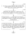
FIG. 7 is a flow chart illustrating a method of establishing data transmission channels for memories. AsFIG. 7 shows, the method includes step S1000 of providing a memory interface chip including a first output channel and a second output channel, wherein the first output channel and the second output channel are used to transmit digital signals with different voltages. In the present embodiment, the first output channel and the second output channel are used to transmit digital signals higher than a core voltage of 1.2 volt and lower than the core voltage of 1.2 volt, respectively, but are not limited thereto. In different embodiments, the first output channel and the second output channel can use other voltage levels as references. - The method further includes step S1010 of receiving data signals from a signal source and inputting the data signal to the memory interface chip. The signal source of the present embodiment is a CMOS image sensor, but is not limited thereto; in different embodiments, the signal source also includes charged-coupled devices or other optical electronic devices that generates analogue or digital signals based on the image sensed.
- In the present embodiment, the method of establishing a data transmission channel includes step S1020 of connecting the memory interface chip to one of memories including a first memory and a second memory. The memory interface chip includes a first data bus and a second data bus to be connected to one of the first memory and the second memory and transmit signals from the signal source and the memory interface chip to one of the first memory and the second memory. In the present embodiment, the first data bus and the second data bus are 16-bit data interfaces. In other words, each of the first data bus and the second data bus has 16 pins.
- The purpose of the first data bus and the second data bus mentioned above changes according to the structure of the memory connected to the memory interface chip. When the memory is a DDR SDRAM, the first data bus and the second data bus are both used to receive digital data from the memory. However, when the memory is a DDR2 SDRAM, the first data bus and the second data bus are used to transmit digital data and memory address, respectively.
- Furthermore, the method of establishing data transmission channels for memories includes step S1030 of closing off one of the first output channel and the second output channel based on the memory connected to the memory interface chip and controlling the other output channel to generate a data voltage based on the data signal received from the signal source.
- When the memory interface chip is connected to the first memory, the memory interface chip forces a second pre-driver of the second output channel into a high output impedance state and conducts a channel switch of the first output channel for transmission purposes. On the other hand, when the memory interface chip is connected to the second memory, the memory interface chip forces the first pre-driver of the first output channel into a high output impedance state and conducts a channel switch of the second output channel for transmission purposes.
- Furthermore, in the embodiment illustrated in
FIG. 7 , the memory interface chip includes a first driver and a second driver used as software to drive different memories. In the present embodiment, when the interface voltage generated by the memory is greater than the core voltage of 1.2 volt, the memory interface chip uses the first driver to control the first output channel to process electrical signals greater than the core voltage of 1.2 volt. On the other hand, when the interface voltage generated by the memory is lower than the core voltage of 1.2 volt, the memory interface chip will use the second driver to control the second output channel to process electrical signals lower than 1.2 volt. - The above is a detailed description of the particular embodiment of the invention which is not intended to limit the invention to the embodiment described. It is recognized that modifications within the scope of the invention will occur to a person skilled in the art. Such modifications and equivalents of the invention are intended for inclusion within the scope of this invention.
Claims (19)
Applications Claiming Priority (3)
| Application Number | Priority Date | Filing Date | Title |
|---|---|---|---|
| TW099142680A TWI425362B (en) | 2010-12-07 | 2010-12-07 | Memory interface chip corresponding to different memories and method of establishing memory transmission channel |
| TW099142680 | 2010-12-07 | ||
| TW099142680A | 2010-12-07 |
Publications (2)
| Publication Number | Publication Date |
|---|---|
| US20120144077A1 true US20120144077A1 (en) | 2012-06-07 |
| US8972636B2 US8972636B2 (en) | 2015-03-03 |
Family
ID=46163317
Family Applications (1)
| Application Number | Title | Priority Date | Filing Date |
|---|---|---|---|
| US13/313,412 Active 2032-04-09 US8972636B2 (en) | 2010-12-07 | 2011-12-07 | Memory interface chip corresponding to different memories and method of establishing memory transmission channel |
Country Status (2)
| Country | Link |
|---|---|
| US (1) | US8972636B2 (en) |
| TW (1) | TWI425362B (en) |
Cited By (1)
| Publication number | Priority date | Publication date | Assignee | Title |
|---|---|---|---|---|
| US11604744B2 (en) * | 2020-10-16 | 2023-03-14 | Alibaba Group Holding Limited | Dual-modal memory interface controller |
Citations (6)
| Publication number | Priority date | Publication date | Assignee | Title |
|---|---|---|---|---|
| US5095798A (en) * | 1989-01-10 | 1992-03-17 | Nintendo Co. Ltd. | Electronic gaming device with pseudo-stereophonic sound generating capabilities |
| US6839788B2 (en) * | 2001-09-28 | 2005-01-04 | Dot Hill Systems Corp. | Bus zoning in a channel independent storage controller architecture |
| US20060031620A1 (en) * | 2004-07-03 | 2006-02-09 | Andreas Jakobs | Memory controller with a plurality of parallel transfer blocks |
| US20070262806A1 (en) * | 2006-05-11 | 2007-11-15 | Thummalapally Damodar R | Level shifting circuit having junction field effect transistors |
| US20080104282A1 (en) * | 2006-11-01 | 2008-05-01 | Sunplus Technology Co., Ltd. | Serial transmission controller, serial transmission decoder and serial transmission method thereof |
| US7877524B1 (en) * | 2007-11-23 | 2011-01-25 | Pmc-Sierra Us, Inc. | Logical address direct memory access with multiple concurrent physical ports and internal switching |
Family Cites Families (3)
| Publication number | Priority date | Publication date | Assignee | Title |
|---|---|---|---|---|
| US6275900B1 (en) * | 1999-01-27 | 2001-08-14 | International Business Machines Company | Hybrid NUMA/S-COMA system and method |
| US8433874B2 (en) * | 2006-12-06 | 2013-04-30 | Mosaid Technologies Incorporated | Address assignment and type recognition of serially interconnected memory devices of mixed type |
| EP2118903A4 (en) * | 2006-12-06 | 2010-01-06 | Mosaid Technologies Inc | System and method of operating memory devices of mixed type |
-
2010
- 2010-12-07 TW TW099142680A patent/TWI425362B/en not_active IP Right Cessation
-
2011
- 2011-12-07 US US13/313,412 patent/US8972636B2/en active Active
Patent Citations (6)
| Publication number | Priority date | Publication date | Assignee | Title |
|---|---|---|---|---|
| US5095798A (en) * | 1989-01-10 | 1992-03-17 | Nintendo Co. Ltd. | Electronic gaming device with pseudo-stereophonic sound generating capabilities |
| US6839788B2 (en) * | 2001-09-28 | 2005-01-04 | Dot Hill Systems Corp. | Bus zoning in a channel independent storage controller architecture |
| US20060031620A1 (en) * | 2004-07-03 | 2006-02-09 | Andreas Jakobs | Memory controller with a plurality of parallel transfer blocks |
| US20070262806A1 (en) * | 2006-05-11 | 2007-11-15 | Thummalapally Damodar R | Level shifting circuit having junction field effect transistors |
| US20080104282A1 (en) * | 2006-11-01 | 2008-05-01 | Sunplus Technology Co., Ltd. | Serial transmission controller, serial transmission decoder and serial transmission method thereof |
| US7877524B1 (en) * | 2007-11-23 | 2011-01-25 | Pmc-Sierra Us, Inc. | Logical address direct memory access with multiple concurrent physical ports and internal switching |
Cited By (1)
| Publication number | Priority date | Publication date | Assignee | Title |
|---|---|---|---|---|
| US11604744B2 (en) * | 2020-10-16 | 2023-03-14 | Alibaba Group Holding Limited | Dual-modal memory interface controller |
Also Published As
| Publication number | Publication date |
|---|---|
| US8972636B2 (en) | 2015-03-03 |
| TW201224761A (en) | 2012-06-16 |
| TWI425362B (en) | 2014-02-01 |
Similar Documents
| Publication | Publication Date | Title |
|---|---|---|
| US9525294B2 (en) | USB device for making I/O pin with intact voltage during charging procedure and related method | |
| US7893718B2 (en) | High-speed multiplexer and semiconductor device including the same | |
| US10347325B1 (en) | DDR4 memory I/O driver | |
| US8466982B2 (en) | Low common mode driver | |
| US8624625B2 (en) | High definition multimedia interface (HDMI) apparatus including termination circuit | |
| US9781372B2 (en) | Driver and image sensing device including the same | |
| CN112715005A (en) | Transmitter circuit with N-type pull-up transistor and low voltage output swing | |
| US8738827B2 (en) | Circuits and methods for providing communication between a memory card and a host device | |
| US11128121B2 (en) | Protection circuit for decoupling a low voltage circuitry from a high voltage circuitry | |
| US8972636B2 (en) | Memory interface chip corresponding to different memories and method of establishing memory transmission channel | |
| US8294512B2 (en) | Bootstrapped clock generator and track-and-hold circuit including the same | |
| JP2018534806A (en) | Power gating device and method | |
| US11019392B2 (en) | Methods and apparatus for an output buffer | |
| US7755684B2 (en) | Row driver circuitry for imaging devices and related method of operation | |
| US9838004B2 (en) | Enhanced protective multiplexer | |
| US20150078102A1 (en) | Nonvolatile semiconductor memory device and data transmission method | |
| CN107452761B (en) | Adaptive body bias circuit for latch prevention | |
| KR20170094832A (en) | Unit Pixel Apparatus and Operation Method Thereof, and CMOS Image Sensor Using That | |
| US7859295B2 (en) | Transmitter apparatus, systems, and methods | |
| US7489574B2 (en) | Sensing circuit for memories | |
| US10171711B1 (en) | De-emphasized image signal transmission | |
| US9660642B2 (en) | Expansion control circuit |
Legal Events
| Date | Code | Title | Description |
|---|---|---|---|
| AS | Assignment |
Owner name: ALPHA IMAGING TECHNOLOGY CORP., TAIWAN Free format text: ASSIGNMENT OF ASSIGNORS INTEREST;ASSIGNORS:LIN, CHUN-FU;SUN, CHIH-KUO;SIGNING DATES FROM 20111205 TO 20111207;REEL/FRAME:027347/0349 |
|
| STCF | Information on status: patent grant |
Free format text: PATENTED CASE |
|
| FEPP | Fee payment procedure |
Free format text: PAT HOLDER NO LONGER CLAIMS SMALL ENTITY STATUS, ENTITY STATUS SET TO UNDISCOUNTED (ORIGINAL EVENT CODE: STOL); ENTITY STATUS OF PATENT OWNER: LARGE ENTITY |
|
| AS | Assignment |
Owner name: MSTAR SEMICONDUCTOR, INC., TAIWAN Free format text: ASSIGNMENT OF ASSIGNORS INTEREST;ASSIGNOR:ALPHA IMAGING TECHNOLOGY CORP.;REEL/FRAME:037401/0611 Effective date: 20151230 |
|
| MAFP | Maintenance fee payment |
Free format text: PAYMENT OF MAINTENANCE FEE, 4TH YEAR, LARGE ENTITY (ORIGINAL EVENT CODE: M1551); ENTITY STATUS OF PATENT OWNER: LARGE ENTITY Year of fee payment: 4 |
|
| AS | Assignment |
Owner name: MEDIATEK INC., TAIWAN Free format text: MERGER;ASSIGNOR:MSTAR SEMICONDUCTOR, INC.;REEL/FRAME:052931/0468 Effective date: 20190115 |
|
| AS | Assignment |
Owner name: XUESHAN TECHNOLOGIES INC., CANADA Free format text: ASSIGNMENT OF ASSIGNORS INTEREST;ASSIGNOR:MEDIATEK INC.;REEL/FRAME:055486/0870 Effective date: 20201223 |
|
| MAFP | Maintenance fee payment |
Free format text: PAYMENT OF MAINTENANCE FEE, 8TH YEAR, LARGE ENTITY (ORIGINAL EVENT CODE: M1552); ENTITY STATUS OF PATENT OWNER: LARGE ENTITY Year of fee payment: 8 |