US20120249093A1 - Power supply controller - Google Patents
Power supply controller Download PDFInfo
- Publication number
- US20120249093A1 US20120249093A1 US13/078,798 US201113078798A US2012249093A1 US 20120249093 A1 US20120249093 A1 US 20120249093A1 US 201113078798 A US201113078798 A US 201113078798A US 2012249093 A1 US2012249093 A1 US 2012249093A1
- Authority
- US
- United States
- Prior art keywords
- voltage
- signal
- output
- generate
- controller
- Prior art date
- Legal status (The legal status is an assumption and is not a legal conclusion. Google has not performed a legal analysis and makes no representation as to the accuracy of the status listed.)
- Granted
Links
Images


Classifications
-
- H—ELECTRICITY
- H02—GENERATION; CONVERSION OR DISTRIBUTION OF ELECTRIC POWER
- H02M—APPARATUS FOR CONVERSION BETWEEN AC AND AC, BETWEEN AC AND DC, OR BETWEEN DC AND DC, AND FOR USE WITH MAINS OR SIMILAR POWER SUPPLY SYSTEMS; CONVERSION OF DC OR AC INPUT POWER INTO SURGE OUTPUT POWER; CONTROL OR REGULATION THEREOF
- H02M3/00—Conversion of dc power input into dc power output
- H02M3/02—Conversion of dc power input into dc power output without intermediate conversion into ac
- H02M3/04—Conversion of dc power input into dc power output without intermediate conversion into ac by static converters
- H02M3/10—Conversion of dc power input into dc power output without intermediate conversion into ac by static converters using discharge tubes with control electrode or semiconductor devices with control electrode
- H02M3/145—Conversion of dc power input into dc power output without intermediate conversion into ac by static converters using discharge tubes with control electrode or semiconductor devices with control electrode using devices of a triode or transistor type requiring continuous application of a control signal
- H02M3/155—Conversion of dc power input into dc power output without intermediate conversion into ac by static converters using discharge tubes with control electrode or semiconductor devices with control electrode using devices of a triode or transistor type requiring continuous application of a control signal using semiconductor devices only
- H02M3/156—Conversion of dc power input into dc power output without intermediate conversion into ac by static converters using discharge tubes with control electrode or semiconductor devices with control electrode using devices of a triode or transistor type requiring continuous application of a control signal using semiconductor devices only with automatic control of output voltage or current, e.g. switching regulators
- H02M3/158—Conversion of dc power input into dc power output without intermediate conversion into ac by static converters using discharge tubes with control electrode or semiconductor devices with control electrode using devices of a triode or transistor type requiring continuous application of a control signal using semiconductor devices only with automatic control of output voltage or current, e.g. switching regulators including plural semiconductor devices as final control devices for a single load
-
- H—ELECTRICITY
- H02—GENERATION; CONVERSION OR DISTRIBUTION OF ELECTRIC POWER
- H02M—APPARATUS FOR CONVERSION BETWEEN AC AND AC, BETWEEN AC AND DC, OR BETWEEN DC AND DC, AND FOR USE WITH MAINS OR SIMILAR POWER SUPPLY SYSTEMS; CONVERSION OF DC OR AC INPUT POWER INTO SURGE OUTPUT POWER; CONTROL OR REGULATION THEREOF
- H02M3/00—Conversion of dc power input into dc power output
- H02M3/02—Conversion of dc power input into dc power output without intermediate conversion into ac
- H02M3/04—Conversion of dc power input into dc power output without intermediate conversion into ac by static converters
- H02M3/10—Conversion of dc power input into dc power output without intermediate conversion into ac by static converters using discharge tubes with control electrode or semiconductor devices with control electrode
- H02M3/145—Conversion of dc power input into dc power output without intermediate conversion into ac by static converters using discharge tubes with control electrode or semiconductor devices with control electrode using devices of a triode or transistor type requiring continuous application of a control signal
- H02M3/155—Conversion of dc power input into dc power output without intermediate conversion into ac by static converters using discharge tubes with control electrode or semiconductor devices with control electrode using devices of a triode or transistor type requiring continuous application of a control signal using semiconductor devices only
- H02M3/156—Conversion of dc power input into dc power output without intermediate conversion into ac by static converters using discharge tubes with control electrode or semiconductor devices with control electrode using devices of a triode or transistor type requiring continuous application of a control signal using semiconductor devices only with automatic control of output voltage or current, e.g. switching regulators
- H02M3/158—Conversion of dc power input into dc power output without intermediate conversion into ac by static converters using discharge tubes with control electrode or semiconductor devices with control electrode using devices of a triode or transistor type requiring continuous application of a control signal using semiconductor devices only with automatic control of output voltage or current, e.g. switching regulators including plural semiconductor devices as final control devices for a single load
- H02M3/1588—Conversion of dc power input into dc power output without intermediate conversion into ac by static converters using discharge tubes with control electrode or semiconductor devices with control electrode using devices of a triode or transistor type requiring continuous application of a control signal using semiconductor devices only with automatic control of output voltage or current, e.g. switching regulators including plural semiconductor devices as final control devices for a single load comprising at least one synchronous rectifier element
-
- H—ELECTRICITY
- H02—GENERATION; CONVERSION OR DISTRIBUTION OF ELECTRIC POWER
- H02M—APPARATUS FOR CONVERSION BETWEEN AC AND AC, BETWEEN AC AND DC, OR BETWEEN DC AND DC, AND FOR USE WITH MAINS OR SIMILAR POWER SUPPLY SYSTEMS; CONVERSION OF DC OR AC INPUT POWER INTO SURGE OUTPUT POWER; CONTROL OR REGULATION THEREOF
- H02M3/00—Conversion of dc power input into dc power output
- H02M3/02—Conversion of dc power input into dc power output without intermediate conversion into ac
- H02M3/04—Conversion of dc power input into dc power output without intermediate conversion into ac by static converters
- H02M3/10—Conversion of dc power input into dc power output without intermediate conversion into ac by static converters using discharge tubes with control electrode or semiconductor devices with control electrode
- H02M3/145—Conversion of dc power input into dc power output without intermediate conversion into ac by static converters using discharge tubes with control electrode or semiconductor devices with control electrode using devices of a triode or transistor type requiring continuous application of a control signal
- H02M3/155—Conversion of dc power input into dc power output without intermediate conversion into ac by static converters using discharge tubes with control electrode or semiconductor devices with control electrode using devices of a triode or transistor type requiring continuous application of a control signal using semiconductor devices only
-
- H—ELECTRICITY
- H02—GENERATION; CONVERSION OR DISTRIBUTION OF ELECTRIC POWER
- H02M—APPARATUS FOR CONVERSION BETWEEN AC AND AC, BETWEEN AC AND DC, OR BETWEEN DC AND DC, AND FOR USE WITH MAINS OR SIMILAR POWER SUPPLY SYSTEMS; CONVERSION OF DC OR AC INPUT POWER INTO SURGE OUTPUT POWER; CONTROL OR REGULATION THEREOF
- H02M1/00—Details of apparatus for conversion
- H02M1/0003—Details of control, feedback or regulation circuits
-
- H—ELECTRICITY
- H02—GENERATION; CONVERSION OR DISTRIBUTION OF ELECTRIC POWER
- H02M—APPARATUS FOR CONVERSION BETWEEN AC AND AC, BETWEEN AC AND DC, OR BETWEEN DC AND DC, AND FOR USE WITH MAINS OR SIMILAR POWER SUPPLY SYSTEMS; CONVERSION OF DC OR AC INPUT POWER INTO SURGE OUTPUT POWER; CONTROL OR REGULATION THEREOF
- H02M3/00—Conversion of dc power input into dc power output
- H02M3/02—Conversion of dc power input into dc power output without intermediate conversion into ac
- H02M3/04—Conversion of dc power input into dc power output without intermediate conversion into ac by static converters
- H02M3/10—Conversion of dc power input into dc power output without intermediate conversion into ac by static converters using discharge tubes with control electrode or semiconductor devices with control electrode
- H02M3/145—Conversion of dc power input into dc power output without intermediate conversion into ac by static converters using discharge tubes with control electrode or semiconductor devices with control electrode using devices of a triode or transistor type requiring continuous application of a control signal
- H02M3/155—Conversion of dc power input into dc power output without intermediate conversion into ac by static converters using discharge tubes with control electrode or semiconductor devices with control electrode using devices of a triode or transistor type requiring continuous application of a control signal using semiconductor devices only
- H02M3/156—Conversion of dc power input into dc power output without intermediate conversion into ac by static converters using discharge tubes with control electrode or semiconductor devices with control electrode using devices of a triode or transistor type requiring continuous application of a control signal using semiconductor devices only with automatic control of output voltage or current, e.g. switching regulators
- H02M3/157—Conversion of dc power input into dc power output without intermediate conversion into ac by static converters using discharge tubes with control electrode or semiconductor devices with control electrode using devices of a triode or transistor type requiring continuous application of a control signal using semiconductor devices only with automatic control of output voltage or current, e.g. switching regulators with digital control
-
- Y—GENERAL TAGGING OF NEW TECHNOLOGICAL DEVELOPMENTS; GENERAL TAGGING OF CROSS-SECTIONAL TECHNOLOGIES SPANNING OVER SEVERAL SECTIONS OF THE IPC; TECHNICAL SUBJECTS COVERED BY FORMER USPC CROSS-REFERENCE ART COLLECTIONS [XRACs] AND DIGESTS
- Y02—TECHNOLOGIES OR APPLICATIONS FOR MITIGATION OR ADAPTATION AGAINST CLIMATE CHANGE
- Y02B—CLIMATE CHANGE MITIGATION TECHNOLOGIES RELATED TO BUILDINGS, e.g. HOUSING, HOUSE APPLIANCES OR RELATED END-USER APPLICATIONS
- Y02B70/00—Technologies for an efficient end-user side electric power management and consumption
- Y02B70/10—Technologies improving the efficiency by using switched-mode power supplies [SMPS], i.e. efficient power electronics conversion e.g. power factor correction or reduction of losses in power supplies or efficient standby modes
Definitions
- the present invention relates generally to power supplies, and more specifically, to systems, device, and methods related to controllers of a switch-mode power supply.
- FIG. 1 is a block diagram of a switch-mode power supply.
- FIG. 2A illustrates a conventional controller within a switch-mode power supply.
- FIG. 2B illustrates a conventional controller within a switch-mode power supply.
- FIG. 3 illustrates a converter coupled to a controller, according to an exemplary embodiment of the present invention.
- FIG. 4 illustrates a controller, in accordance with an exemplary embodiment of the present invention.
- FIGS. 5-10 illustrate simulation results of a controller, in accordance with an exemplary embodiment of the present invention.
- FIG. 11 illustrates waveforms associated with a controller, according to an exemplary embodiment of the present invention.
- FIG. 12 illustrates waveforms associated with a buck power stage coupled to a controller, in accordance with an exemplary embodiment of the present invention.
- FIG. 13 illustrates additional waveforms associated with a controller, according to an exemplary embodiment of the present invention.
- FIG. 14 illustrates a time error
- FIG. 15 illustrates another converter coupled to a controller, according to an exemplary embodiment of the present invention.
- FIGS. 16 and 17 illustrate simulation results of a controller, in accordance with an exemplary embodiment of the present invention.
- FIG. 18A illustrates a pseudo-random data generator base on a 4-bit shift register.
- FIG. 18B illustrates a delay line
- FIG. 19A illustrates waveforms associated with a conventional converter in steady-state.
- FIG. 19B is a plot depicting a spectrum of an input current of the conventional converter.
- FIG. 20A illustrates waveforms associated with a conventional converter under a repetitive load transient.
- FIG. 20B is a plot depicting a spectrum of an input current of the conventional converter.
- FIG. 21A illustrates waveforms associated with a controller, according to an exemplary embodiment of the present invention.
- FIG. 21B is a plot depicting a spectrum of the input current of a controller, in accordance with an exemplary embodiment of the present invention.
- FIG. 22A illustrates additional waveforms associated with a controller, according to an exemplary embodiment of the present invention.
- FIG. 22B is a plot depicting a spectrum of the input current of a controller, in accordance with an exemplary embodiment of the present invention.
- FIGS. 23-27 illustrate waveforms associated with a controller, according to an exemplary embodiment of the present invention.
- FIG. 28 illustrates a circuit diagram of a comparator.
- FIGS. 29 and 30 illustrate additional waveforms associated with a controller, according to an exemplary embodiment of the present invention.
- FIGS. 31 and 32 illustrate additional waveforms associated with a controller, according to an exemplary embodiment of the present invention.
- FIG. 33 illustrates a block diagram of an on-chip implementation of a controller, according to an exemplary embodiment of the present invention.
- FIG. 34 is a flowchart illustrating another method, in accordance with an exemplary embodiment of the present invention.
- FIG. 1 illustrates a conventional switch-mode power supply (SMPS) 100 including a power stage 102 and a controller 104 .
- SMPS switch-mode power supply
- FIG. 1 illustrates a conventional switch-mode power supply (SMPS) 100 including a power stage 102 and a controller 104 .
- SMPS switch-mode power supply
- fast recovery from load transients, minimizing output filter size, and simple controller implementation are of key importance. These issues are especially important in low-power, high-volume systems supplying mobile devices, consumer electronics, and numerous other applications consuming power from a fraction of watt to several hundreds of watts.
- proximity time-optimal controllers have been proposed in hopes of achieving steady state in a single on-off switching action (i.e., fast recovery time).
- time-optimal systems were developed as analog solutions, using a second order switching surface (i.e., geometric control principles), which can be also relate to sliding mode control.
- the switching surface based controller defines a path for one or more state variables (in accordance with possible combinations of the state values) of the controlled object (i.e., switching power converter), and accordingly forces the states to follow the path.
- the simplest example of a first order switching surface controller is a hysteretic controller, where the state of the output voltage is dictated by the reference value of a comparator.
- inductor current is also often controlled. The controlled inductor current is either directly measured or estimated by measuring the output capacitor current or voltage.
- PWM controllers are a preferable solution due to the simplicity of their implementation.
- exemplary embodiments of the present invention relate to systems, devices, and methods for control within a switch-mode power supply. It is noted that the embodiments of the present invention are applicable to many power conversion topologies as well as non-linear or switched-mode amplification of signals. Exemplary embodiments, as described herein, may provide a hardware efficient control solution that improves transient response times (i.e., improve system dynamics).
- a controller in accordance with an exemplary embodiment, may be implemented with hardware that is comparable or even simpler than that needed for voltage-mode PWM realization or Class D amplification.
- exemplary embodiments may reduce SMPS electromagnetic interference (EMI), which may be an extremely important feature in numerous noise-sensitive applications.
- EMI electromagnetic interference
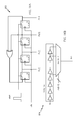
- FIG. 3 illustrates a device 300 including a controller 302 and a power stage 301 , according to an exemplary embodiment of the present invention.
- Controller 302 which may be referred to herein as a one-bit controller, includes an adder 304 , an amplifier 306 , an adder 308 , a comparator 310 , a programmable delay line 312 , a inverter 314 , and a low-pass filter 316 .
- low-pass filter 316 may comprise a first order low pass filter.
- Power stage 301 comprises an input voltage Vbatt, an inductor L, a capacitor C, a load 318 , a first transistor MS (i.e., main switch), a second transistor SR (synchronous rectifier), gate drivers 320 and 322 , and an output voltage Vout.
- first transistor MS i.e., main switch
- second transistor SR synchronous rectifier
- adder 304 is configured to receive each of a reference voltage Vref and output voltage Vout, and, in response thereto, output an error signal E(t).
- Amplifier 306 is configured to amplify error signal E(t), which is then received by adder 308 . It is noted that amplifier 306 may reduce the error within device 301 . It is noted that amplifier 306 may be omitted (i.e., the gain is equal to 1) if the error is tolerable by the application.
- Adder 308 also receives reference voltage Vref, and, in response thereto, outputs a voltage Vcmp, which is provided to an inverting input of comparator 310 .
- a non-inverting input of comparator 310 is configured to receive an estimated voltage Vest, which is output from low-pass filter 316 .
- a signal b(t) output from comparator 310 is provided to programmable delay line 312 and an output of programmable delay line 312 is provided to inverter 314 .
- Inverter 314 is configured to convey a signal 6 (t), which is received by low-pass filter 316 .
- emulator 313 of the power stage where, in steady state, the signal at the output of filter 316 (i.e., V est ) is substantially the same as output voltage V out .
- V est the signal at the output of filter 316
- One difference between emulator 313 and power stage 301 which, in this case, is a second order system, is that emulator 313 has a lower order dynamic, allowing simplified regulation of estimated voltage V est and, consequently, output voltage V out at the desired reference voltage V ref .
- Different implementation of this portion of the circuit can be accomplished, as long as the final equation representing the combination of the terms remains consistent (i.e., one term could be added to the other input of the comparison with inverted sign, etc.).
- estimated voltage V est is substantially similar to the desired output voltage, kept at that level by a loop consisting of comparator 310 and delay line 312 ; a different ratio of reference voltage, estimator output and converter output voltages can be obtained by properly scaling the variables.
- Delay line 312 may be configured to determine comparator triggering latency and, consequently, the oscillation frequency of the loop (i.e., the converter switching frequency).
- signal ⁇ (t) output from inverter 314 has substantially the same duty ratio as output b(t) of comparator 310 , and an amplitude equal to input voltage V batt providing feedforward for emulator 313 .
- a waveform of signal ⁇ (t) is substantially similar to a switching voltage V sw of power stage 301 .
- the waveform of signal ⁇ (t) may be affected by both emulator 313 and disturbances of output voltage Vout. In steady state (i.e., when the difference between Vout and Vref is substantially zero), the duty ratio of signal ⁇ (t) is determined entirely by emulator 313 .
- a duty ratio signal ⁇ (t) may also be influenced by error signal E(t), which represents the difference between the desired, reference voltage V ref and the actual value of output voltage V out .
- error signal E(t) is amplified and added to the inverting input of the comparator 310 .
- compensator latency which may exist in conventional controllers, due to integral action, may be eliminated, the duty ratio of signal ⁇ (t) is affected, and substantially instantaneous reaction to disturbances (i.e., fast recovery of the output voltage), is achieved.
- controller 302 may comprise a single pole system, which is intrinsically stable. As will be appreciated by a person having ordinary skill in the art, controller 302 may be faster than systems including a compensator.
- FIG. 4 illustrates a controller 352 , which is one contemplated implementation of controller 302 shown in FIG. 3 .
- controller 352 comprises a filter (i.e., low-pass filter 316 ) comprising resistor Rf and capacitor Cf, a first amplifier 354 and a second amplifier 356 .
- Controller 352 further includes programmable delay line 312 having an output coupled to inverter 314 .
- output voltage V out and reference voltage V ref may be coupled to first amplifier 354 and an output of inverter 314 may be provided to a gate driver of a power stage (e.g., power stage 301 ).
- Controller 352 may further include means of amplification 354 , which may be implemented with an operational amplifier as shown, or other means, and may be simply a summing input of the comparator 356 , if no amplification is necessary.
- resistor Rf may comprise a 1K ohm resistor
- resistor R 2 may comprise a 1M ohm resistor
- resistor R 3 may comprise a 100K ohm resistor
- capacitor Cf may comprise a 2 nF capacitor.
- controller 302 in steady state may be regulated by a feed-forward regulated oscillator with a digitally programmable delay line 312 that, together with an RC filter 316 , forms emulator 313 of the power stage.
- FIGS. 6-10 Simulation results of a model (not shown) of device 300 , wherein inductor L of power stage 301 comprises 0.3 ⁇ H and capacitor C of power stage 301 comprises 4.7 ⁇ F, are shown in FIGS. 6-10 .
- a wavefrom 362 of represents a voltage at capacitor Cf of filter 316
- a waveform 364 represents signal ⁇ (t)
- a waveform 366 represents input voltage V batt .
- the output of the low-pass filter i.e., V est
- V est the output of the low-pass filter
- FIGS. 6 to 9 demonstrate load transient responses of controller 302 for several various output capacitor and input voltage values, including a case wherein input voltage V batt is slightly higher than output voltage V out , making inductor slew rate very small.
- FIG. 7 illustrates simulation results of a 6 V to 2V buck converter for load changes between 1 A and 3 A and a value of power stage output capacitor (i.e., capacitor C) of 4.7 ⁇ F.
- a waveform 368 represents output voltage V out
- a waveform 370 represents a current in inductor L
- a waveform 372 represents signal ⁇ ( 4
- FIG. 7 illustrates simulation results of a 6 V to 0.9V buck converter for load changes between 0.68 A and 2.68 A and a value of a power stage output capacitor (i.e., capacitor C) of 22 ⁇ F.
- a waveform 374 represents output voltage V out
- a waveform 376 represents a current in inductor L
- a waveform 378 represents signal ⁇ (t)
- a waveform 380 represents input voltage V batt .
- FIG. 8 illustrates simulation results of a buck converter for step input voltage changes between 2V and 1.5V.
- a waveform 382 represents output voltage V out
- a waveform 384 represents a current in inductor L
- a waveform 386 represents signal ⁇ (t)
- a waveform 388 represents input voltage V batt .
- FIG. 9 illustrates simulation results of a buck converter for linear input voltage changes between 3V and 6V.
- a waveform 390 represents output voltage V out
- a waveform 392 represents a current in inductor L
- a waveform 394 represents signal ⁇ (t)
- a waveform 396 represents input voltage V batt .
- FIG. 10 illustrates simulation results of a 0.9V buck converter for input voltage V batt changes between 0.5V and 6V, including under-voltage conditions.
- a waveform 398 of represents output voltage V out
- a waveform 400 represents a current in inductor L
- a waveform 402 represents signal ⁇ (t)
- a waveform 404 represents input voltage V batt .
- amplifier 306 may substantially instantaneously change the non-inverting input of comparator 310 causing substantially immediate action of controller 302 and the suppression of the transient.
- controller 302 may recover to steady state through a single on-off switching action. It is noted that the demonstrated transient response is comparable to that of other proximal time-optimal solutions and has no significant current overshoots, which may exist in hysteretic implementations.
- the results of the simulations illustrated in FIGS. 8-10 verify that controller 302 may be able to quickly compensate for disturbance in input voltage V batt .
- the simulations further illustrate that controller 302 is able to recover from under voltage conditions when, over a brief period, input voltage V batt drops below output voltage Vout.
- v h and v l are the maximum and minimum allowable output voltage (i.e., output voltage V out ) values, respectively.
- i h and i l are defined as the maximum and minimum currents through the inductor L, respectively.
- inductor L has a value equal to 0.3 ⁇ H and capacitor C has a value equal to 3.9 ⁇ F, performance for the given constraints may be enhanced.
- waveforms of emulator 313 in steady state may be approximated with those shown in FIG. 11 .
- Each switching interval can be divided into parts, where T + is the time needed for a voltage at filter 316 to reach the threshold of the comparator 310 after a low-to-high transition of signal ⁇ (t), T d is the propagation time of delay line 312 , and T ⁇ is the time interval needed for the voltage at filter 316 to reach the threshold after a high-to-low transition of signal ⁇ (t).
- V batt - V ref RC f ⁇ T d V ref RC f ⁇ T - ( 4 )
- V batt - V ref RC f ⁇ T + V ref RC f ⁇ T d ( 5 )
- T + V ref V batt - V ref ⁇ T d ( 6 )
- turn on time t on DT sw , where D is the duty ratio of signal ⁇ ,
- switching period T sw of the device 300 is defined as:
- time-domain analysis is combined with an energy balance principle.
- This may comprise a multi-step procedure that allows a designer to set the recovery time and peak/minimum inductor current during transient or, equivalently, the maximum output voltage deviation.
- the gain calculation procedure can be described as follows: In a first step, based on the size of the load transient, peak current limit, and the type of the transient, the variation in the on or off time of the main switch is calculated as:
- ⁇ i L is the difference between initial and the peak/valley value of a current through inductor L during the transient and v L is the voltage across inductor L during that period.
- the peak inductor value can be selected such that saturation of the inductor core is avoided.
- a waveform 406 represents output voltage V out
- a waveform 408 represents a current in filter 316
- a waveform 410 represents signal ⁇ (t). It is noted that with reference to FIG. 12 , the required change of the comparator voltage (i.e. the change across the estimator's capacitor Cf) is:
- Equation 11 illustrates the required change of a voltage of capacitor Cf of filter 316 needed to achieve the inductor current change of ⁇ i L in a single on/off switching action.
- the gain of the error amplifier 306 is calculated as the ratio of voltage deviations of capacitor Cf and the output voltage Vout. Accordingly:
- ⁇ v out is the output voltage deviation.
- Idealized transient power stage 301 , controller 302 , and RC filter 316 waveforms of FIG. 13 may be observed.
- a waveform 412 represents output voltage V out
- a waveform 414 represents a current through inductor L
- a waveform 416 represents a current through load 318
- a waveform 418 represents a voltage at an inverting input of comparator 310
- a waveform 420 represents a voltage at a non-inverting input of comparator 310
- a waveform 422 represents signal ⁇ (t).
- the output voltage deviation due to the load change ⁇ i load comprises of three components, namely, the initial drop due to the current passing through the equivalent series resistance of the output capacitor C (i.e., R esr i c ), a drop due to the delayed action of amplifier 306 and comparator 310 (i.e., ⁇ v out1 ), and the deviation caused by the delayed reaction of power stage 310 (i.e., ⁇ v out2 ).
- the resistance R esr caused voltage drop vanishes in time, as the capacitor current recovers to zero, and only the last two components influence the charge-balance based gain selection.
- ⁇ v out1 can be calculated as:
- T dcmp is combined delay of amplifier 306 and comparator 310 .
- the second component can be calculated as:
- T cn is the time interval the inductor current needs to change from the initial to the new load value.
- the amplified value of this error needs to be larger or equal to the deviation calculated in step 2 above. Accordingly:
- the waveforms of FIG. 12 also show that the peak current of inductor L is larger than the maximum current through load 318 , due to the existence of an extra delay in the switching action T d , caused by delay line 312 .
- This equation also indicates that by increasing the gain A, the time constant of estimator 313 can be reduced, possibly allowing a full on-chip implementation.
- controller 302 is selected such that at the output voltage valley/peak point, time instant comparator 310 is triggered.
- the gain RCf product can be selected such that a maximum allowable current deviation ⁇ i L is reached at the triggering point. In general, the selection based on the maximum current does not reduce voltage deviation but, in some cases, can result in a shorter recovery time.
- a waveform 424 represents output voltage Vout
- a waveform 426 represents error voltage E(t)
- a waveform 428 represents a current through load 318
- a waveform 430 represents a current through inductor L.
- R esr is the equivalent resistance of output capacitor C
- ⁇ I load is the load step value
- m RC is the slope of the RC f emulator voltage error
- t vp is the ideal time required to reach the triggering point where the inductor and load currents are the same
- t vp * is the actual estimator time required to reach the valley point
- ⁇ t vp is the difference between the two times (i.e., the value of delay/lead in the triggering).
- equation (18) is calculated to obtain the following expression for output voltage V out :
- v out V ref + R esr ⁇ ( - ⁇ ⁇ ⁇ I load + v in - v out L ⁇ t ) + 1 C ⁇ ( - ⁇ ⁇ ⁇ I load ⁇ t + v in - v out 2 ⁇ L ⁇ t 2 ) ( 19 )
- V ref is the reference dc voltage
- v in is the input voltage of device 300
- i c is the capacitor current ( ⁇ i Load (t) ⁇ i L (t)).
- the RC emulator circuit voltage is given by:
- V RC V ref - v in - v out R f ⁇ C f ⁇ t ( 20 )
- Rf is the emulator resistance and Cf its capacitance.
- the RC f product can also be given by:
- controller 302 compensates for any extreme error in the triggering point. This can be explained by looking at waveforms of FIG. 12 . Due to convex nature of the amplified error signal curve, for a large range of the gains and the estimator voltage slopes a response close to time optimal will occur.
- emulator waveforms are virtually the same as those of the switching converter.
- emulator 313 and power stage 301 produce slightly different voltages.
- the losses usually cause the DC output voltage of the converter to be smaller than that of the low-pass filter and, consequently, a nonzero error at the input of differential amplifier 306 of FIG. 3 .
- the difference between two voltages is:
- A is the gain of the differential amplifier and V err the steady state value of the error signal.
- the previously described regulation error can be utilized to further minimize the size of output capacitor C through voltage droop technique as well as for a rough estimation of the output load current.
- the output voltage is not kept at the constant value for all operating conditions. Instead, at heavier loads the voltage is set to be a little bit lower than the reference allowing for larger overshoots during heavy-to-light load transients. Similarly, for the lighter loads the output voltage is increased, as shown in FIG. 12 . It can also be seen that the utilization of the voltage droop technique reduces the peak inductor current, further minimizing the output filter size.
- device 300 of FIG. 3 can be modified as shown in FIG. 15 , to minimize the influence of the semiconductor losses and consequently the steady state error.
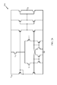
- a device 500 including a controller 502 and power stage 301 (e.g., of a buck converter), according to an exemplary embodiment of the present invention.
- Controller 502 includes an adder 304 , an amplifier 306 , an adder 308 , a comparator 310 , a programmable delay line 312 , a inverter 314 , and a low-pass filter 316 .
- filter 316 of controller 502 is directly supplied from a switching node 505 .
- This provides the same voltage at the inputs of the power stage LC filter and filter 316 of the emulator.
- the power stage filter i.e., inductor L and capacitor C
- controller 502 compares the average value of the switching voltage (i.e., V sw ) with V est .
- Controller 502 is simulated using a model (not shown) and compared to a model of controller 302 .
- a converter with 60 m ⁇ of the equivalent semiconductor losses and 40 m ⁇ filter losses was used for controller 502 .
- the results of simulations are shown in FIGS. 16 and 17 .
- a waveform 560 represents output voltage Vout
- a waveform 562 represents a current through inductor L
- a waveform 564 represents signal ⁇ (t).
- a waveform 566 represents output voltage Vout
- a waveform 568 represents a current through inductor L
- a waveform 570 represents signal ⁇ (t). It is noted that the proposed modification (i.e., controller 502 ) reduces voltage error in comparison to controller 302 and, thus regulation is significantly improved.
- the presented controller architecture allows a simple implementation of a feature for the reduction of electromagnetic interface (EMI) caused by the operation of the converter at a fixed frequency.
- EMI electromagnetic interface
- V batt is supply voltage
- V ref the output voltage reference
- the switching frequency of the converter can be regulated by varying the propagation time of the delay line in accordance with a pre-defined pattern. More importantly, in this system, the duty ratio of the buck converter does not depend on the propagation time of the delay line and, consequently, any change of the propagation time that is at the rate slower or equal to the switching rate does not require any correcting action that would be used for maintaining voltage regulation, significantly simplifying implementation of noise reduction techniques. With reference to FIG. 11 , since all the current waveforms are linear, any increase in T d causes a proportional increase of T + and T ⁇ intervals and, consequently, of the transistor on-time as well as of the overall switching period of the converter.
- a pseudo-random data generator such as pseudo-random data generator 572 illustrated in FIG. 18A
- data generator 572 creates a pseudo-random sequence of numbers that is used to dynamically change the length (i.e., propagation time of delay line 574 ) in each switching cycle.
- a model (not shown) of data generator 572 was used to verify operation of the EMI reduction system. Simulation results of the model of a data generator used to verify operation of the EMI reduction system are shown in FIGS.
- FIGS. 19A and 19B illustrate operation of a conventional controller in steady-state.
- waveform 578 represents output voltage Vout
- waveform 580 represents a current through inductor L
- waveform 582 represents a switching frequency.
- a waveform 584 represents a spectrum of an input current.
- FIGS. 20A and 20B illustrate operation of a conventional controller under a repetitive load transient wherein a load transient frequency is equal to 125 kHz.
- waveform 586 represents output voltage Vout
- waveform 588 represents a current through inductor L
- waveform 590 represents a switching frequency.
- a waveform 592 represents a spectrum of an input current.
- FIGS. 21A and 21B illustrate operation of a controller, according to an exemplary embodiment of the present invention, with a spread spectrum generator in steady-state.
- waveform 594 represents output voltage Vout
- waveform 596 represents a current through inductor L
- waveform 598 represents a switching frequency.
- a waveform 600 represents a spectrum of an input current.
- FIGS. 22A and 22B illustrate operation of a controller, according to an exemplary embodiment of the present invention, with a spread spectrum generator with a repetitive load of 125 kHz.
- waveform 602 represents output voltage Vout
- waveform 604 represents a current through inductor L
- waveform 606 represents a switching frequency.
- a waveform 608 represents a spectrum of an input current.
- controllers 302 and 502 To verify operation of controllers 302 and 502 and analyze practical implementation issues, an experimental prototype using discrete components was built, based on controller 302 of FIG. 3 and controller 502 of FIG. 15 . In addition, the controllers and power stage (without inductors and capacitors) are also designed in 0.13 ⁇ m process. As described in the following subsections, the discrete implementation has proven feasibility of the system. At the same time, it has shown that the discrete implementation significantly limits the switching frequency and/or affects the transient performance of the system.
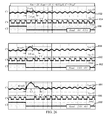
- FIGS. 23 and 24 Experimental results confirming stable steady-state operation of devices 300 and 500 are shown in FIGS. 23 and 24 . Operation for three different input voltages is shown in FIG. 23 .
- signals 610 , 612 , and 614 respectively represent output voltage Vout, switching node voltage V sw , and a load step signal for an input voltage of 2V.
- signals 616 , 618 , and 620 respectively represent output voltage Vout, switching node voltage V sw , and a load step signal for an input voltage of 3V.
- signals 622 , 624 , and 626 respectively represent output voltage Vout, switching node voltage V sw , and a load step signal for an input voltage of 4V.
- the results are presented for the minimum delay case and confirm the validity of describing relation between the switching frequency, propagation time of the delay elements, and the steady-state operating conditions.
- FIG. 24 shows operation of the system as the propagation time of the delay cells changes “on-line”.
- signals 628 , 630 , and 632 respectively represent output voltage Vout, switching node voltage V sw , and a frequency change signal. It can be seen that the system is able to instantaneously change the switching frequency allowing implementation of the EMI mitigation method based on frequency variation, which was described above.
- FIGS. 25 and 26 Dynamic response tests of the experimental prototype, which is based on devices 300 and 500 , operating at the maximum switching frequency (i.e. minimum propagation time) are shown in FIGS. 25 and 26 .
- signals 634 , 636 , and 638 respectively represent output voltage Vout, switching node voltage V sw , and a load step signal for a load current variation of 0.0 A to 0.5 A.
- signals 640 , 642 , and 644 respectively represent output voltage Vout, switching node voltage V sw , and a load step signal for a load current variation of 0.0 A to 1.0 A.
- signals 646 , 648 , and 650 respectively represent output voltage Vout, switching node voltage V sw , and a load step signal a load current variation of 0.0 A to 2.0 A.
- signals 652 , 654 , and 656 respectively represent output voltage Vout, switching node voltage V sw , and a load step signal for a load current variation of 0.5A to 0.0A.
- signals 658 , 660 , and 662 respectively represent output voltage Vout, switching node voltage V sw , and a load step signal for a load current variation of 1.0 A to 0.0 A.
- signals 664 , 666 , and 668 respectively represent output voltage Vout, switching node voltage V sw , and a load step signal a load current variation of 2.0 A to 0.0 A.
- the response is tested over a wide range of input voltage values as well as for different load transients. It can be noticed that for 0 to 0.5 A and 0.5 A to 1 A the system recovers in a less than two switching cycles, even though, the reaction of the controller is barely noticeable on the diagrams.
- These waveforms actually confirm a very accurate controller operation that does not introduce current or overstress. This can be explained by calculating ideal t on time needed for the controller to increase the current by a given load step value:
- the needed time t on varies between 60 ns (for 5 V input and 0.5 A current step) to 170 ns (for 3 V input and 1 A current step), which, in all cases, correspond to a minor increase of the duty ratio value.
- signals 670 , 672 , and 674 respectively represent output voltage Vout, switching node voltage V sw , and a load step signal for an input voltage of 5V and an output voltage of 1V. It can be seen that the reaction of the controller to the output voltage deviation is delayed by about 250 ns.
- This time corresponds to the total contribution of the component delays (the gate driver ( ⁇ 90 ns), FPGA ( ⁇ 80 ns), op-amp ( ⁇ 20 ns), the comparator ( ⁇ 10 ns), plus parasitic delays of the PCB).
- the output voltage drops by more than 35 mV before the controller is able to react.
- the delayed detection is followed by the controller reaction (e.g., about 300 ns increase in the ratio value corresponding to the 2 A current increase for the given operating condition), which in a no-delay case would correspond to the proximity time optimal response.
- the initial reaction of the controller, resulting in equal inductor and load currents, is followed by a 250 ns t off time that, as depicted in FIG. 11 , is again caused by the delay line.
- the previously described delays may be due to the discrete implementation of the experimental setup.
- FIGS. 29 and 30 demonstrate dynamic characteristics of device 300 depicted in FIG. 3 (i.e., the controller in which the signal for the low-pass filter is provided by a rail-to-rail inverter).
- FIG. 29 illustrates a light-to-heavy load transient response
- FIG. 34 illustrates a heavy-to-light transient response.
- signals 676 , 678 , 680 , and 682 respectively represent a load step current, a current through inductor L, signal ⁇ (t), and output voltage Vout.
- signals 684 , 686 , 688 , and 690 respectively represent a load step current, a current through inductor L, signal ⁇ (t), and output voltage Vout. In this case, to speed up the system performance the delay line is temporarily bypassed upon the initial transient is detected.
- FIGS. 31 and 32 demonstrate dynamic characteristics of device 500 depicted in FIG. 17 .
- FIG. 35 illustrates a light-to-heavy load transient response
- FIG. 32 illustrates a heavy-to-light transient response.
- signals 692 , 694 , 696 , and 698 respectively represent a load step current, a current through inductor L, signal ⁇ (t), and output voltage Vout.
- signals 700 , 702 , 704 , and 706 respectively represent a load step current, a current through inductor L, signal ⁇ (t), and output voltage Vout.
- the delay line is temporarily bypassed upon the initial transient is detected.
- FIG. 33 illustrates a simplified block diagram of a possible on-chip implementation of controllers 302 and 502 .
- controller 302 / 502 may include additional blocks and/or input that allow its modification and possible utilization of additional digital features.
- inverter 710 is a rail-to-rail inverter (see FIGS. 3 and 15 ) used to provide input for the emulator filter during transient conditions and a possible implementation of the voltage droop based control or/and current estimation.
- Delay line 714 is programmable current starved cells or some other programmable delay structure allowing implementation of EMI reduction techniques and synchronization with an external clock signal.
- EMI 712 is an optional block for creating spread spectrum signal for minimizing EMI.
- “Synch” comprises an input for an external synchronization clock.
- “Ssc” comprises an input for adjustments of EMI 712 .
- “Bypass” comprises an input for bypassing the delay line minimizes delay in the system reaction, improving transient response. As described above, bypassing the delay line improves transient response during transients.
- Comparator 716 is the comparator of FIGS. 3 and 15 .
- Amplifier 718 is the operational amplifier of FIGS. 3 and 15 .
- Output “load_est” is an output that can be used for monitoring the state of the error signal and, consequently, load estimation in the steady-state.
- “Vref” and “vout” are two inputs of amplifier 718 .
- Emulator Filter 720 is a part of a complete RCf circuit of the emulator filter.
- “Cf” comprises is a pin for connecting additional filtering capacitor.
- Filter input select 722 is configured to select the input for the filter based on the conditions in the circuit. In steady state, to minimize the error, the filter can be fed from the switching node of the converter ( FIG. 15 ). During transients, it can be driven by the inverter ( FIG. 3 ) to minimize delays.
- “Sel” comprises a control signal for selecting the filter input.
- “Vsw” comprises an input for the signal coming from the switching node.
- reference voltage Vref may comprise an audio signal of the power amplifier.
- FIG. 34 is a flowchart illustrating a method 990 , in accordance with one or more exemplary embodiments.
- Method 990 may include amplifying an error voltage comprising a difference between a voltage output from a power stage and a reference voltage (depicted by numeral 992 ).
- Method 990 may further include comparing a summation voltage comprising a sum of an amplified error voltage and the reference voltage with an estimated voltage to generate a comparator output signal (depicted by numeral 994 ).
- method 990 may include generating a gate drive signal from the comparator output signal (depicted by numeral 996 ).
- method 990 may include filtering a signal coupled to the power stage to generate the estimated voltage (depicted by numeral 998 ).
- DSP Digital Signal Processor
- ASIC Application Specific Integrated Circuit
- FPGA Field Programmable Gate Array
- a general purpose processor may be a microprocessor, but in the alternative, the processor may be any conventional processor, controller, microcontroller, or state machine.
- a processor may also be implemented as a combination of computing devices, e.g., a combination of a DSP and a microprocessor, a plurality of microprocessors, one or more microprocessors in conjunction with a DSP core, or any other such configuration.
- a software module may reside in Random Access Memory (RAM), flash memory, Read Only Memory (ROM), Electrically Programmable ROM (EPROM), Electrically Erasable Programmable ROM (EEPROM), registers, hard disk, a removable disk, a CD-ROM, or any other form of storage medium known in the art.
- An exemplary storage medium is coupled to the processor such that the processor can read information from, and write information to, the storage medium.
- the storage medium may be integral to the processor.
- the processor and the storage medium may reside in an ASIC.
- the ASIC may reside in a user terminal.
- the processor and the storage medium may reside as discrete components in a user terminal.
- the functions described may be implemented in hardware, software, firmware, or any combination thereof. If implemented in software, the functions may be stored on or transmitted over as one or more instructions or code on a computer-readable medium.
- Computer-readable media includes both computer storage media and communication media including any medium that facilitates transfer of a computer program from one place to another.
- a storage media may be any available media that can be accessed by a computer.
- such computer-readable media can comprise RAM, ROM, EEPROM, CD-ROM or other optical disk storage, magnetic disk storage or other magnetic storage devices, or any other medium that can be used to carry or store desired program code in the form of instructions or data structures and that can be accessed by a computer.
- any connection is properly termed a computer-readable medium.
- the software is transmitted from a website, server, or other remote source using a coaxial cable, fiber optic cable, twisted pair, digital subscriber line (DSL), or wireless technologies such as infrared, radio, and microwave
- the coaxial cable, fiber optic cable, twisted pair, DSL, or wireless technologies such as infrared, radio, and microwave are included in the definition of medium.
- Disk and disc includes compact disc (CD), laser disc, optical disc, digital versatile disc (DVD), floppy disk and blu-ray disc where disks usually reproduce data magnetically, while discs reproduce data optically with lasers. Combinations of the above should also be included within the scope of computer-readable media.
Abstract
Description
- 1. Field
- The present invention relates generally to power supplies, and more specifically, to systems, device, and methods related to controllers of a switch-mode power supply.
- 2. Background
- With regard to switch-mode power supply controllers, fast recovery from load transients, minimizing output filter size, and simple implementation are of key importance. These issues are especially important in low-power, high-volume systems supplying mobile devices, consumer electronics, and numerous other applications consuming power from a fraction of watt to several hundreds of watts. Conventional hysteretic implementations suffer from large current stress, as well as stability related problems caused by overly large energy inertia. Furthermore, although time-optimal controllers result in improved responses, the hardware required for the implementation of such systems is overly expensive for the targeted cost-sensitive systems. As a consequence, pulse-width modulated (PWM) controllers implementing linear control laws are predominantly used, even though they exhibit significantly slower dynamic response and, consequently, require significantly large filtering components.
- A need exists for enhanced methods, systems, and devices related to control of a power supply.
-
FIG. 1 is a block diagram of a switch-mode power supply. -
FIG. 2A illustrates a conventional controller within a switch-mode power supply. -
FIG. 2B illustrates a conventional controller within a switch-mode power supply. -
FIG. 3 illustrates a converter coupled to a controller, according to an exemplary embodiment of the present invention. -
FIG. 4 illustrates a controller, in accordance with an exemplary embodiment of the present invention. -
FIGS. 5-10 illustrate simulation results of a controller, in accordance with an exemplary embodiment of the present invention. -
FIG. 11 illustrates waveforms associated with a controller, according to an exemplary embodiment of the present invention. -
FIG. 12 illustrates waveforms associated with a buck power stage coupled to a controller, in accordance with an exemplary embodiment of the present invention. -
FIG. 13 illustrates additional waveforms associated with a controller, according to an exemplary embodiment of the present invention. -
FIG. 14 illustrates a time error. -
FIG. 15 illustrates another converter coupled to a controller, according to an exemplary embodiment of the present invention. -
FIGS. 16 and 17 illustrate simulation results of a controller, in accordance with an exemplary embodiment of the present invention. -
FIG. 18A illustrates a pseudo-random data generator base on a 4-bit shift register. -
FIG. 18B illustrates a delay line. -
FIG. 19A illustrates waveforms associated with a conventional converter in steady-state. -
FIG. 19B is a plot depicting a spectrum of an input current of the conventional converter. -
FIG. 20A illustrates waveforms associated with a conventional converter under a repetitive load transient. -
FIG. 20B is a plot depicting a spectrum of an input current of the conventional converter. -
FIG. 21A illustrates waveforms associated with a controller, according to an exemplary embodiment of the present invention. -
FIG. 21B is a plot depicting a spectrum of the input current of a controller, in accordance with an exemplary embodiment of the present invention. -
FIG. 22A illustrates additional waveforms associated with a controller, according to an exemplary embodiment of the present invention. -
FIG. 22B is a plot depicting a spectrum of the input current of a controller, in accordance with an exemplary embodiment of the present invention. -
FIGS. 23-27 illustrate waveforms associated with a controller, according to an exemplary embodiment of the present invention. -
FIG. 28 illustrates a circuit diagram of a comparator. -
FIGS. 29 and 30 illustrate additional waveforms associated with a controller, according to an exemplary embodiment of the present invention. -
FIGS. 31 and 32 illustrate additional waveforms associated with a controller, according to an exemplary embodiment of the present invention. -
FIG. 33 illustrates a block diagram of an on-chip implementation of a controller, according to an exemplary embodiment of the present invention. -
FIG. 34 is a flowchart illustrating another method, in accordance with an exemplary embodiment of the present invention. - The detailed description set forth below in connection with the appended drawings is intended as a description of exemplary embodiments of the present invention and is not intended to represent the only embodiments in which the present invention can be practiced. The term “exemplary” used throughout this description means “serving as an example, instance, or illustration,” and should not necessarily be construed as preferred or advantageous over other exemplary embodiments. The detailed description includes specific details for the purpose of providing a thorough understanding of the exemplary embodiments of the invention. It will be apparent to those skilled in the art that the exemplary embodiments of the invention may be practiced without these specific details. In some instances, well-known structures and devices are shown in block diagram form in order to avoid obscuring the novelty of the exemplary embodiments presented herein.
-
FIG. 1 illustrates a conventional switch-mode power supply (SMPS) 100 including apower stage 102 and acontroller 104. As will be understood by a person having ordinary skill in the art, with regard to switch-mode power supplies, fast recovery from load transients, minimizing output filter size, and simple controller implementation are of key importance. These issues are especially important in low-power, high-volume systems supplying mobile devices, consumer electronics, and numerous other applications consuming power from a fraction of watt to several hundreds of watts. - As alternatives to predominantly used voltage mode pulse-width modulation (PWM) controllers implementing linear proportional-integral (PI) or proportional-integral-derivative (PID) control laws, numerous solutions for developing a controller having improved transient response have been proposed. Namely, various hysteretic and time-optimal controller architectures, resulting in simplified implementation and improved load transient response times, respectively, have been reported. Hysteretic controllers have proven to be a hardware-efficient solution for obtaining fast transient response with a small number of components. Realization of such a controller usually requires a hysteretic comparator and, in some cases, additional circuitry for frequency regulation, which can be done through threshold variation or through variation of the sampling rate. The main drawback of conventional hysteretic implementations is overly large current stress, requiring overdesign of the semiconductor switches and filtering components, as well as stability related problems caused by overly large energy inertia.
- Furthermore, proximity time-optimal controllers have been proposed in hopes of achieving steady state in a single on-off switching action (i.e., fast recovery time). Initially, time-optimal systems were developed as analog solutions, using a second order switching surface (i.e., geometric control principles), which can be also relate to sliding mode control. The switching surface based controller defines a path for one or more state variables (in accordance with possible combinations of the state values) of the controlled object (i.e., switching power converter), and accordingly forces the states to follow the path. The simplest example of a first order switching surface controller is a hysteretic controller, where the state of the output voltage is dictated by the reference value of a comparator. In second order systems, in addition to the output voltage, inductor current is also often controlled. The controlled inductor current is either directly measured or estimated by measuring the output capacitor current or voltage.
- Even though second order switching surface based controllers were proposed many years ago, they have not been widely adopted. This is mostly due to the complexity of algorithms required for their implementation, making the controllers unsuitable for analog realization, which has been predominant in low-power dc-dc converters. Recent progress in the digital control of low-power dc-dc converters has enabled development of switching surface based controller prototypes, nearly resulting in the time-optimal response. The same progress has also allowed for the development of alternative control algorithms for obtaining time-optimal response, based on capacitor charge balance principle.
- Further, although the presented time-optimal controllers result in improved responses (i.e., drastically reduce the output filter size), they have not been widely adopted in low-power dc-dc systems. Hardware required for the implementation of such systems is overly expensive for the targeted cost-sensitive systems. As a consequence, pulse-width modulated (PWM) controllers, similar to
PWM controllers FIG. 2 , are still predominantly used. Even though they exhibit significantly slower dynamic response and, consequently, require significantly large filtering components (i.e., the power inductor L and the output capacitor C), PWM controllers are a preferable solution due to the simplicity of their implementation. - Various exemplary embodiments of the present invention, as described herein, relate to systems, devices, and methods for control within a switch-mode power supply. It is noted that the embodiments of the present invention are applicable to many power conversion topologies as well as non-linear or switched-mode amplification of signals. Exemplary embodiments, as described herein, may provide a hardware efficient control solution that improves transient response times (i.e., improve system dynamics). A controller, in accordance with an exemplary embodiment, may be implemented with hardware that is comparable or even simpler than that needed for voltage-mode PWM realization or Class D amplification. Furthermore, exemplary embodiments may reduce SMPS electromagnetic interference (EMI), which may be an extremely important feature in numerous noise-sensitive applications.
-
FIG. 3 illustrates adevice 300 including acontroller 302 and apower stage 301, according to an exemplary embodiment of the present invention.Controller 302, which may be referred to herein as a one-bit controller, includes anadder 304, anamplifier 306, anadder 308, acomparator 310, aprogrammable delay line 312, ainverter 314, and a low-pass filter 316. By way of example, low-pass filter 316 may comprise a first order low pass filter.Power stage 301 comprises an input voltage Vbatt, an inductor L, a capacitor C, aload 318, a first transistor MS (i.e., main switch), a second transistor SR (synchronous rectifier),gate drivers 320 and 322, and an output voltage Vout. - As illustrated in
FIG. 3 ,adder 304 is configured to receive each of a reference voltage Vref and output voltage Vout, and, in response thereto, output an error signal E(t).Amplifier 306 is configured to amplify error signal E(t), which is then received byadder 308. It is noted thatamplifier 306 may reduce the error withindevice 301. It is noted thatamplifier 306 may be omitted (i.e., the gain is equal to 1) if the error is tolerable by the application.Adder 308 also receives reference voltage Vref, and, in response thereto, outputs a voltage Vcmp, which is provided to an inverting input ofcomparator 310. A non-inverting input ofcomparator 310 is configured to receive an estimated voltage Vest, which is output from low-pass filter 316. A signal b(t) output fromcomparator 310 is provided toprogrammable delay line 312 and an output ofprogrammable delay line 312 is provided toinverter 314.Inverter 314 is configured to convey a signal 6(t), which is received by low-pass filter 316. - It is noted that
programmable delay line 312,inverter 314,comparator 310, and filter 316 form anemulator 313 of the power stage where, in steady state, the signal at the output of filter 316 (i.e., Vest) is substantially the same as output voltage Vout. One difference betweenemulator 313 andpower stage 301, which, in this case, is a second order system, is thatemulator 313 has a lower order dynamic, allowing simplified regulation of estimated voltage Vest and, consequently, output voltage Vout at the desired reference voltage Vref. Different implementation of this portion of the circuit can be accomplished, as long as the final equation representing the combination of the terms remains consistent (i.e., one term could be added to the other input of the comparison with inverted sign, etc.). In this implementation, estimated voltage Vest is substantially similar to the desired output voltage, kept at that level by a loop consisting ofcomparator 310 anddelay line 312; a different ratio of reference voltage, estimator output and converter output voltages can be obtained by properly scaling the variables.Delay line 312 may be configured to determine comparator triggering latency and, consequently, the oscillation frequency of the loop (i.e., the converter switching frequency). - It is further noted that signal δ(t) output from
inverter 314 has substantially the same duty ratio as output b(t) ofcomparator 310, and an amplitude equal to input voltage Vbatt providing feedforward foremulator 313. According to one exemplary embodiment, a waveform of signal δ(t) is substantially similar to a switching voltage Vsw ofpower stage 301. The waveform of signal δ(t) may be affected by bothemulator 313 and disturbances of output voltage Vout. In steady state (i.e., when the difference between Vout and Vref is substantially zero), the duty ratio of signal δ(t) is determined entirely byemulator 313. During load transients and other disturbances that change a value of output voltage Vout, a duty ratio signal δ(t) may also be influenced by error signal E(t), which represents the difference between the desired, reference voltage Vref and the actual value of output voltage Vout. As soon as a non-zero error occurs, error signal E(t) is amplified and added to the inverting input of thecomparator 310. As a result, compensator latency, which may exist in conventional controllers, due to integral action, may be eliminated, the duty ratio of signal δ(t) is affected, and substantially instantaneous reaction to disturbances (i.e., fast recovery of the output voltage), is achieved. It is noted that, although not required,delay line 312 fine tunes the self-oscillating frequency ofcontroller 302. It is further noted thatcontroller 302 may comprise a single pole system, which is intrinsically stable. As will be appreciated by a person having ordinary skill in the art,controller 302 may be faster than systems including a compensator. -
FIG. 4 illustrates acontroller 352, which is one contemplated implementation ofcontroller 302 shown inFIG. 3 . As illustrated inFIG. 4 ,controller 352 comprises a filter (i.e., low-pass filter 316) comprising resistor Rf and capacitor Cf, afirst amplifier 354 and asecond amplifier 356.Controller 352 further includesprogrammable delay line 312 having an output coupled toinverter 314. Moreover, output voltage Vout and reference voltage Vref may be coupled tofirst amplifier 354 and an output ofinverter 314 may be provided to a gate driver of a power stage (e.g., power stage 301).Controller 352 may further include means ofamplification 354, which may be implemented with an operational amplifier as shown, or other means, and may be simply a summing input of thecomparator 356, if no amplification is necessary. As non-limiting examples, resistor Rf may comprise a 1K ohm resistor, resistor R2 may comprise a 1M ohm resistor, resistor R3 may comprise a 100K ohm resistor, and capacitor Cf may comprise a 2 nF capacitor. - As described above, an operation of
controller 302 in steady state may be regulated by a feed-forward regulated oscillator with a digitallyprogrammable delay line 312 that, together with anRC filter 316, forms emulator 313 of the power stage. - Simulation results of a model (not shown) of
device 300, wherein inductor L ofpower stage 301 comprises 0.3 μH and capacitor C ofpower stage 301 comprises 4.7 μF, are shown inFIGS. 6-10 . With reference toFIGS. 3 , 4, and 5, awavefrom 362 of represents a voltage at capacitor Cf offilter 316, awaveform 364 represents signal δ(t), and awaveform 366 represents input voltage Vbatt. It is noted that the output of the low-pass filter (i.e., Vest), which is depicted bysignal 362, has a value which approximates the output voltage Vout as well as the average voltage at the switching node (i.e., voltage Vswt). -
FIGS. 6 to 9 demonstrate load transient responses ofcontroller 302 for several various output capacitor and input voltage values, including a case wherein input voltage Vbatt is slightly higher than output voltage Vout, making inductor slew rate very small. Specifically,FIG. 7 illustrates simulation results of a 6 V to 2V buck converter for load changes between 1 A and 3 A and a value of power stage output capacitor (i.e., capacitor C) of 4.7 μF. With reference toFIGS. 3 , 4, and 7, awaveform 368 represents output voltage Vout, awaveform 370 represents a current in inductor L, and awaveform 372 represents signal δ(4 -
FIG. 7 illustrates simulation results of a 6 V to 0.9V buck converter for load changes between 0.68 A and 2.68 A and a value of a power stage output capacitor (i.e., capacitor C) of 22 μF. With reference toFIGS. 3 , 4, and 7, awaveform 374 represents output voltage Vout, awaveform 376 represents a current in inductor L, awaveform 378 represents signal δ(t), and awaveform 380 represents input voltage Vbatt.FIG. 8 illustrates simulation results of a buck converter for step input voltage changes between 2V and 1.5V. With reference toFIGS. 3 , 4, and 8, awaveform 382 represents output voltage Vout, awaveform 384 represents a current in inductor L, awaveform 386 represents signal δ(t), and awaveform 388 represents input voltage Vbatt.FIG. 9 illustrates simulation results of a buck converter for linear input voltage changes between 3V and 6V. With reference toFIGS. 3 , 4, and 9, awaveform 390 represents output voltage Vout, awaveform 392 represents a current in inductor L, awaveform 394 represents signal δ(t), and awaveform 396 represents input voltage Vbatt.FIG. 10 illustrates simulation results of a 0.9V buck converter for input voltage Vbatt changes between 0.5V and 6V, including under-voltage conditions. With reference toFIG. 10 , awaveform 398 of represents output voltage Vout, awaveform 400 represents a current in inductor L, awaveform 402 represents signal δ(t), and awaveform 404 represents input voltage Vbatt. - During transients,
amplifier 306 may substantially instantaneously change the non-inverting input ofcomparator 310 causing substantially immediate action ofcontroller 302 and the suppression of the transient. As will be appreciated by a person having ordinary skill in the art,controller 302 may recover to steady state through a single on-off switching action. It is noted that the demonstrated transient response is comparable to that of other proximal time-optimal solutions and has no significant current overshoots, which may exist in hysteretic implementations. The results of the simulations illustrated inFIGS. 8-10 verify thatcontroller 302 may be able to quickly compensate for disturbance in input voltage Vbatt. The simulations further illustrate thatcontroller 302 is able to recover from under voltage conditions when, over a brief period, input voltage Vbatt drops below output voltage Vout. - Selection of components within
power stage 301 will now be described. It is noted that the following description related to selection of power stage components is provided as an example and exemplary embodiments may comprise any suitable components. It is noted that fordevice 300, current and voltage overshoots may depend on physical constrains ofpower stage 301. Hence, the selection of the power stage components may be crucial for proper system design, minimizing overall size of the filtering components, and limiting the stress on the semiconductor and filter components. The selection is based on the energy balance criteria, where the maximum output voltage deviation and the maximum current stress (i.e., maximum inductor current difference) are taken as the design constrains. As the initial point in this analysis, the amount of energy loss Ec during maximum allowable voltage deviation of capacitor C is given by: -
- where, vh and vl are the maximum and minimum allowable output voltage (i.e., output voltage Vout) values, respectively.
- During load transients, a voltage at capacitor C is recovered by providing the same amount of energy from inductor L, hence the energy balance equation becomes:
-
- where ih and il are defined as the maximum and minimum currents through the inductor L, respectively.
- For example, for a 6V to 2V buck converter, with a 2 A maximum load change and 150 mV overshoot during a heavy-to-light load transient, if inductor L has a value equal to 0.3 μH and capacitor C has a value equal to 3.9 μF, performance for the given constraints may be enhanced.
- Selection of components of
filter 316 and the propagation time of thedelay line 312 ofcontroller 302 will now be described. It is noted that the following description related to selection of filter components and the propagation time of thedelay line 312 is provided as an example and exemplary embodiments may comprise any suitable components. It is noted that since a feedback loop that regulates steady state operation ofconverter 302 is closed aroundemulator 313, parameters of the feedback loop may dictate the switching frequency ofconverter 302. To simplify the analysis of the operation ofemulator 313, small-ripple approximation and system linearization, as will be understood by a person having ordinary skill in the art, are applied. It is assumed that the switching frequency fsw=1/Tsw ofconverter 300 is significantly higher than the corner frequency (i.e., fRC=1/(2 πRCf)) of filter 316 (e.g., fsw>10 fRC) such that the ripple across capacitor Cf ofFIG. 4 is negligible: -
Δvest— ripple<<Vest≈Vref (3) - Under such assumptions, waveforms of
emulator 313 in steady state may be approximated with those shown inFIG. 11 . Each switching interval can be divided into parts, where T+ is the time needed for a voltage atfilter 316 to reach the threshold of thecomparator 310 after a low-to-high transition of signal δ(t), Td is the propagation time ofdelay line 312, and T− is the time interval needed for the voltage atfilter 316 to reach the threshold after a high-to-low transition of signal δ(t). - By looking at the waveforms and equating the expressions for the capacitor ripple for both portions of the switching interval, one may calculate T+ and T31 time intervals, and consequently the period of oscillations as follows:
-
- Combining equations (4) and (5) gives expressions for T+ interval
-
- Moreover, turn on time ton=DTsw, where D is the duty ratio of signal δ,
-
- wherein the switching period Tsw of the
device 300 is defined as: -
- These equations illustrate how the key timing intervals depend on the circuit parameters and prove that the switching frequency of
device 300 can be changed by varying the propagation time ofdelay line 312. - As an example, optimal gain calculation will now be described. To calculate the optimal gain of the
device 300, time-domain analysis is combined with an energy balance principle. This may comprise a multi-step procedure that allows a designer to set the recovery time and peak/minimum inductor current during transient or, equivalently, the maximum output voltage deviation. The gain calculation procedure can be described as follows: In a first step, based on the size of the load transient, peak current limit, and the type of the transient, the variation in the on or off time of the main switch is calculated as: -
- where ΔiL is the difference between initial and the peak/valley value of a current through inductor L during the transient and vL is the voltage across inductor L during that period. The peak inductor value can be selected such that saturation of the inductor core is avoided.
- In a second step, the amount of change in the estimator's comparator voltage Vamp (see
FIGS. 3 and 4 ) required to create the previously defined time variation is calculated. This calculation is performed by adopting linear approximation described above. With reference toFIGS. 3 and 11 , awaveform 406 represents output voltage Vout, awaveform 408 represents a current infilter 316, and awaveform 410 represents signal δ(t). It is noted that with reference toFIG. 12 , the required change of the comparator voltage (i.e. the change across the estimator's capacitor Cf) is: -
- wherein VR is the voltage across resistor R1. By combining equations (9) and (10), the following equation may be obtained:
-
-
Equation 11 illustrates the required change of a voltage of capacitor Cf offilter 316 needed to achieve the inductor current change of ΔiL in a single on/off switching action. In another step, the gain of theerror amplifier 306 is calculated as the ratio of voltage deviations of capacitor Cf and the output voltage Vout. Accordingly: -
- wherein Δvout is the output voltage deviation. Idealized
transient power stage 301,controller 302, andRC filter 316 waveforms ofFIG. 13 may be observed. With reference toFIGS. 3 and 12 , awaveform 412 represents output voltage Vout, awaveform 414 represents a current through inductor L, awaveform 416 represents a current throughload 318, awaveform 418 represents a voltage at an inverting input ofcomparator 310, awaveform 420 represents a voltage at a non-inverting input ofcomparator 310, and awaveform 422 represents signal δ(t). - It can be seen that that the output voltage deviation due to the load change Δiload comprises of three components, namely, the initial drop due to the current passing through the equivalent series resistance of the output capacitor C (i.e., Resric), a drop due to the delayed action of
amplifier 306 and comparator 310 (i.e., Δvout1), and the deviation caused by the delayed reaction of power stage 310 (i.e., Δvout2). However, as explained herein, the resistance Resr caused voltage drop vanishes in time, as the capacitor current recovers to zero, and only the last two components influence the charge-balance based gain selection. Δvout1 can be calculated as: -
- wherein Tdcmp is combined delay of
amplifier 306 andcomparator 310. - The second component can be calculated as:
-
- wherein Tcn is the time interval the inductor current needs to change from the initial to the new load value. For a light-to-heavy load change in a buck converter this time interval is:
-
- At the end of this interval, the output voltage error E(t) (
FIGS. 3 and 4 ) is maximum, as well as the non-inverting input ofcomparator 310. It should be noted, that at this point, a current in capacitor C is substantially zero and, consequently, Resric has no influence on the voltage drop. By combining equations (13) and (14) an equation for the maximum voltage drop may be obtained: -
- In order to prevent premature triggering of the main switch, the amplified value of this error needs to be larger or equal to the deviation calculated in
step 2 above. Accordingly: -
- The waveforms of
FIG. 12 also show that the peak current of inductor L is larger than the maximum current throughload 318, due to the existence of an extra delay in the switching action Td, caused bydelay line 312. This equation also indicates that by increasing the gain A, the time constant ofestimator 313 can be reduced, possibly allowing a full on-chip implementation. - As described above, the action of
controller 302 is selected such that at the output voltage valley/peak point, timeinstant comparator 310 is triggered. Alternatively, instead at the valley point, the gain RCf product can be selected such that a maximum allowable current deviation ΔiL is reached at the triggering point. In general, the selection based on the maximum current does not reduce voltage deviation but, in some cases, can result in a shorter recovery time. -
FIG. 13 illustrates the effect of a potential mismatch between LC and RCf constant, where the initial selection of the parameters is based on the valley point triggering. To simplify explanation, it is assumed that, during the initial response to a load transient, the propagation time ofdelay line 312 is reduced to zero and that the gain A=1. - With reference to
FIGS. 3 and 13 , awaveform 424 represents output voltage Vout, awaveform 426 represents error voltage E(t), awaveform 428 represents a current throughload 318, and awaveform 430 represents a current through inductor L. InFIG. 13 , Resr is the equivalent resistance of output capacitor C, ΔIload is the load step value, mRC is the slope of the RCf emulator voltage error, tvp is the ideal time required to reach the triggering point where the inductor and load currents are the same, tvp* is the actual estimator time required to reach the valley point, and Δtvp is the difference between the two times (i.e., the value of delay/lead in the triggering). - The consequence of this time-mismatch is that, at the triggering point, the inductor current and the load currents are not the same, resulting in a Δivp difference. This effect is quantified through the following mathematical analysis. The AC value of the output voltage Vout during transient is given by:
-
- wherein equation (18) is calculated to obtain the following expression for output voltage Vout:
-
- wherein Vref is the reference dc voltage, vin is the input voltage of
device 300, and ic is the capacitor current (−iLoad(t)−iL(t)). - The RC emulator circuit voltage is given by:
-
- wherein Rf is the emulator resistance and Cf its capacitance.
- By equating (19) and (20), the time required to reach the triggering point (i.e., where the output voltage and the emulator voltage cross) can be derived, as shown in the following equation:
-
- On the other side, the ideal time required to the reach the valley point, calculated by looking at
FIG. 13 , is: -
- In the case of the ideal matching, i.e. tvp* equal to tvp, the RCf product can also be given by:
-
- showing the ideal RCf constant for a given load step.
- For the case when a gain is taken into account, this equation becomes:
-
- The analysis above shows that a change in the input voltage Vin/Vbatt, load step value, or output capacitance may introduce a sub-optimal RC emulator response. This dependence is quantified in
FIG. 14 showing the triggering time delay error for a 5V to 1V buck converter, with a 20 uF output capacitor (i.e., capacitor C), and expected 2 A load step value. It should be noted that expressing the error through the triggering delay allows us to calculate a current overshoot to compared to the case of triggering at the iL=iload point to be calculated for any given operating condition and inductance value. - It should be noted that the natural action of
controller 302, to a large extent, compensates for any extreme error in the triggering point. This can be explained by looking at waveforms ofFIG. 12 . Due to convex nature of the amplified error signal curve, for a large range of the gains and the estimator voltage slopes a response close to time optimal will occur. - Ideally, when a lossless switching converter is controlled, the emulator waveforms are virtually the same as those of the switching converter. However, in reality, due to conduction and switching losses for the same value of the duty ratio of signal δ(t),
emulator 313 andpower stage 301 produce slightly different voltages. The losses usually cause the DC output voltage of the converter to be smaller than that of the low-pass filter and, consequently, a nonzero error at the input ofdifferential amplifier 306 ofFIG. 3 . The difference between two voltages is: -
v diff =V est −V out =AV err (25) - wherein A is the gain of the differential amplifier and Verr the steady state value of the error signal.
- To quantify this error and explain its dependence on the operating conditions, a DC model of non-ideal switching buck converter including switching component losses and a DC model of filter 316 (i.e., ideal DC converter) can be compared. It can be seen that for the same duty ratio delivered to both
power stage 301 andfilter 316,filter 316 produces an output voltage that is larger by: -
v diff ≈I load R loss =A(V ref −V out) (26) - For example, in a case when the switchers having Ron resistance of approximately 100 mΩ are used and the amplifier gain A is 10, at 2.5 A of the output current (78% efficient converter for a 0.9V output) the offset in voltage regulation, due to this error, is about 25 mV.
- The previously described regulation error can be utilized to further minimize the size of output capacitor C through voltage droop technique as well as for a rough estimation of the output load current. In the voltage droop techniques, the output voltage is not kept at the constant value for all operating conditions. Instead, at heavier loads the voltage is set to be a little bit lower than the reference allowing for larger overshoots during heavy-to-light load transients. Similarly, for the lighter loads the output voltage is increased, as shown in
FIG. 12 . It can also be seen that the utilization of the voltage droop technique reduces the peak inductor current, further minimizing the output filter size. - It is noted that by regulating the gain of the differential amplifier (i.e.,
amplifier 306 and adder 304), inherent voltage droop feature can be achieved. Furthermore, the voltage difference at the output of the differential amplifier can be measured to obtain a rough estimate of the output load value. - For the case when the voltage droop is not applicable,
device 300 ofFIG. 3 can be modified as shown inFIG. 15 , to minimize the influence of the semiconductor losses and consequently the steady state error. - With reference to
FIG. 15 , adevice 500 is illustrated including acontroller 502 and power stage 301 (e.g., of a buck converter), according to an exemplary embodiment of the present invention.Controller 502 includes anadder 304, anamplifier 306, anadder 308, acomparator 310, aprogrammable delay line 312, ainverter 314, and a low-pass filter 316. - In contrast to
controller 302, filter 316 ofcontroller 502 is directly supplied from a switchingnode 505. This provides the same voltage at the inputs of the power stage LC filter and filter 316 of the emulator. As a result, the impact of the semiconductor losses on the voltage regulation is eliminated. Now, the only discrepancy between the dc values of vout(t) and vest(t) may occur due to the losses of the power stage filter (i.e., inductor L and capacitor C), which, in general, are significantly smaller than the semiconductor losses, and may be omitted, as in the case of filter-less audio amplifiers. In other words,controller 502 compares the average value of the switching voltage (i.e., Vsw) with Vest. -
Controller 502 is simulated using a model (not shown) and compared to a model ofcontroller 302. Forcontroller 502, a converter with 60 mΩ of the equivalent semiconductor losses and 40 mΩ filter losses was used. The results of simulations are shown inFIGS. 16 and 17 . With reference toFIGS. 3 and 16 , awaveform 560 represents output voltage Vout, awaveform 562 represents a current through inductor L, and awaveform 564 represents signal δ(t). With reference toFIGS. 15 and 17 , awaveform 566 represents output voltage Vout, awaveform 568 represents a current through inductor L, and awaveform 570 represents signal δ(t). It is noted that the proposed modification (i.e., controller 502) reduces voltage error in comparison tocontroller 302 and, thus regulation is significantly improved. - The presented controller architecture allows a simple implementation of a feature for the reduction of electromagnetic interface (EMI) caused by the operation of the converter at a fixed frequency. In the previous analysis it was shown that the switching frequency of the buck converter is:
-
- where, for
device 300 ofFIG. 3 , Vbatt is supply voltage, Vref the output voltage reference, and τd propagation time of the delay line. This equation indicates that the switching frequency of the converter can be regulated by varying the propagation time of the delay line in accordance with a pre-defined pattern. More importantly, in this system, the duty ratio of the buck converter does not depend on the propagation time of the delay line and, consequently, any change of the propagation time that is at the rate slower or equal to the switching rate does not require any correcting action that would be used for maintaining voltage regulation, significantly simplifying implementation of noise reduction techniques. With reference toFIG. 11 , since all the current waveforms are linear, any increase in Td causes a proportional increase of T+ and T− intervals and, consequently, of the transistor on-time as well as of the overall switching period of the converter. - Implementation of the EMI reduction technique, according to an exemplary embodiment, will now be described. To create spread spectrum around the switching frequency a pseudo-random data generator, such as
pseudo-random data generator 572 illustrated inFIG. 18A , is utilized and, accordingly, the original delay line is modified as shown indelay line 574 ofFIG. 18B . As will be appreciated by a person having ordinary skill in the art,data generator 572 creates a pseudo-random sequence of numbers that is used to dynamically change the length (i.e., propagation time of delay line 574) in each switching cycle. A model (not shown) ofdata generator 572 was used to verify operation of the EMI reduction system. Simulation results of the model of a data generator used to verify operation of the EMI reduction system are shown inFIGS. 19A-22B . It should be noted that other techniques besides pseudo-random number generation may be used for changing the time delay (i.e., frequency) and obtaining EMI reduction. For example, sigma-delta modulation and other well-known techniques may be used. -
FIGS. 19A and 19B illustrate operation of a conventional controller in steady-state. With reference toFIG. 19A ,waveform 578 represents output voltage Vout,waveform 580 represents a current through inductor L, andwaveform 582 represents a switching frequency. With reference toFIG. 19B , awaveform 584 represents a spectrum of an input current.FIGS. 20A and 20B illustrate operation of a conventional controller under a repetitive load transient wherein a load transient frequency is equal to 125 kHz. With reference toFIG. 20A ,waveform 586 represents output voltage Vout,waveform 588 represents a current through inductor L, andwaveform 590 represents a switching frequency. With reference toFIG. 20B , awaveform 592 represents a spectrum of an input current.FIGS. 21A and 21B illustrate operation of a controller, according to an exemplary embodiment of the present invention, with a spread spectrum generator in steady-state. With reference toFIG. 21A ,waveform 594 represents output voltage Vout,waveform 596 represents a current through inductor L, andwaveform 598 represents a switching frequency. With reference toFIG. 21B , awaveform 600 represents a spectrum of an input current.FIGS. 22A and 22B illustrate operation of a controller, according to an exemplary embodiment of the present invention, with a spread spectrum generator with a repetitive load of 125 kHz. With reference toFIG. 22A ,waveform 602 represents output voltage Vout,waveform 604 represents a current through inductor L, andwaveform 606 represents a switching frequency. With reference toFIG. 22B , awaveform 608 represents a spectrum of an input current. - It is noted that the waveforms depicted in
FIGS. 19A-22B demonstrate thatpseudo-random data generator 572 may significantly reduce large spectrum components. It can also be seen that under a variable load the spectrum of the signal is also affected, due to the fast controller action. - To verify operation of
controllers controller 302 ofFIG. 3 andcontroller 502 ofFIG. 15 . In addition, the controllers and power stage (without inductors and capacitors) are also designed in 0.13 μm process. As described in the following subsections, the discrete implementation has proven feasibility of the system. At the same time, it has shown that the discrete implementation significantly limits the switching frequency and/or affects the transient performance of the system. - Experimental results confirming stable steady-state operation of
devices FIGS. 23 and 24 . Operation for three different input voltages is shown inFIG. 23 . With reference toFIG. 23 , signals 610, 612, and 614 respectively represent output voltage Vout, switching node voltage Vsw, and a load step signal for an input voltage of 2V. Furthermore, signals 616, 618, and 620 respectively represent output voltage Vout, switching node voltage Vsw, and a load step signal for an input voltage of 3V. Moreover, signals 622, 624, and 626 respectively represent output voltage Vout, switching node voltage Vsw, and a load step signal for an input voltage of 4V. The results are presented for the minimum delay case and confirm the validity of describing relation between the switching frequency, propagation time of the delay elements, and the steady-state operating conditions. -
FIG. 24 shows operation of the system as the propagation time of the delay cells changes “on-line”. With reference toFIG. 24 , signals 628, 630, and 632 respectively represent output voltage Vout, switching node voltage Vsw, and a frequency change signal. It can be seen that the system is able to instantaneously change the switching frequency allowing implementation of the EMI mitigation method based on frequency variation, which was described above. - Dynamic response tests of the experimental prototype, which is based on
devices FIGS. 25 and 26 . With reference toFIG. 25 , signals 634, 636, and 638 respectively represent output voltage Vout, switching node voltage Vsw, and a load step signal for a load current variation of 0.0 A to 0.5 A. Furthermore, signals 640, 642, and 644 respectively represent output voltage Vout, switching node voltage Vsw, and a load step signal for a load current variation of 0.0 A to 1.0 A. Moreover, signals 646, 648, and 650 respectively represent output voltage Vout, switching node voltage Vsw, and a load step signal a load current variation of 0.0 A to 2.0 A. With reference toFIG. 26 , signals 652, 654, and 656 respectively represent output voltage Vout, switching node voltage Vsw, and a load step signal for a load current variation of 0.5A to 0.0A. Furthermore, signals 658, 660, and 662 respectively represent output voltage Vout, switching node voltage Vsw, and a load step signal for a load current variation of 1.0 A to 0.0 A. Moreover, signals 664, 666, and 668 respectively represent output voltage Vout, switching node voltage Vsw, and a load step signal a load current variation of 2.0 A to 0.0 A. The response is tested over a wide range of input voltage values as well as for different load transients. It can be noticed that for 0 to 0.5 A and 0.5 A to 1 A the system recovers in a less than two switching cycles, even though, the reaction of the controller is barely noticeable on the diagrams. These waveforms actually confirm a very accurate controller operation that does not introduce current or overstress. This can be explained by calculating ideal ton time needed for the controller to increase the current by a given load step value: -
- For the given operating conditions, in the experimental circuit, the needed time ton varies between 60 ns (for 5 V input and 0.5 A current step) to 170 ns (for 3 V input and 1 A current step), which, in all cases, correspond to a minor increase of the duty ratio value.
- For large heavy-to-light load transients a significant difference between the simulated and actual response exists causing a large than expected voltage deviation. This difference can be explained by looking at
FIG. 27 showing zoomed version of the output voltage waveform during a transient. With reference toFIG. 27 , signals 670, 672, and 674 respectively represent output voltage Vout, switching node voltage Vsw, and a load step signal for an input voltage of 5V and an output voltage of 1V. It can be seen that the reaction of the controller to the output voltage deviation is delayed by about 250 ns. This time corresponds to the total contribution of the component delays (the gate driver (˜90 ns), FPGA (˜80 ns), op-amp (˜20 ns), the comparator (˜10 ns), plus parasitic delays of the PCB). - It can be seen that, due to the delays, the output voltage drops by more than 35 mV before the controller is able to react. The delayed detection is followed by the controller reaction (e.g., about 300 ns increase in the ratio value corresponding to the 2 A current increase for the given operating condition), which in a no-delay case would correspond to the proximity time optimal response. The initial reaction of the controller, resulting in equal inductor and load currents, is followed by a 250 ns toff time that, as depicted in
FIG. 11 , is again caused by the delay line. The previously described delays may be due to the discrete implementation of the experimental setup. - To test performance of a potential on-chip controller implementation, and show that the delays may be reduced, simulations were performed based on a cadence setup. All the system components except the operational amplifier are designed using IBM 0.13 μm process. Those include power stage and gate drivers, programmable current-starved delay cells, and the rail-to-rail buffer/inverter and
comparator 310 ofFIG. 28 . In the simulations the operational amplifier is an abstract Verilog A block. The switching frequency of the designed system is 2.5 MHz. For the emulator's LP filter the following values of the components are used C=200 pF and Rf=4 KΩ. -
FIGS. 29 and 30 demonstrate dynamic characteristics ofdevice 300 depicted inFIG. 3 (i.e., the controller in which the signal for the low-pass filter is provided by a rail-to-rail inverter).FIG. 29 illustrates a light-to-heavy load transient response andFIG. 34 illustrates a heavy-to-light transient response. With reference toFIG. 29 , signals 676, 678, 680, and 682 respectively represent a load step current, a current through inductor L, signal δ(t), and output voltage Vout. With reference toFIG. 30 , signals 684, 686, 688, and 690 respectively represent a load step current, a current through inductor L, signal δ(t), and output voltage Vout. In this case, to speed up the system performance the delay line is temporarily bypassed upon the initial transient is detected. -
FIGS. 31 and 32 demonstrate dynamic characteristics ofdevice 500 depicted inFIG. 17 .FIG. 35 illustrates a light-to-heavy load transient response andFIG. 32 illustrates a heavy-to-light transient response. With reference toFIG. 35 , signals 692, 694, 696, and 698 respectively represent a load step current, a current through inductor L, signal δ(t), and output voltage Vout. With reference toFIG. 32 , signals 700, 702, 704, and 706 respectively represent a load step current, a current through inductor L, signal δ(t), and output voltage Vout. Again, to minimize the controller reaction time, the delay line is temporarily bypassed upon the initial transient is detected. -
FIG. 33 illustrates a simplified block diagram of a possible on-chip implementation ofcontrollers controller 302/502 may include additional blocks and/or input that allow its modification and possible utilization of additional digital features. More specifically,inverter 710 is a rail-to-rail inverter (seeFIGS. 3 and 15 ) used to provide input for the emulator filter during transient conditions and a possible implementation of the voltage droop based control or/and current estimation.Delay line 714 is programmable current starved cells or some other programmable delay structure allowing implementation of EMI reduction techniques and synchronization with an external clock signal.EMI 712 is an optional block for creating spread spectrum signal for minimizing EMI. “Synch” comprises an input for an external synchronization clock. “Ssc” comprises an input for adjustments ofEMI 712. “Bypass” comprises an input for bypassing the delay line minimizes delay in the system reaction, improving transient response. As described above, bypassing the delay line improves transient response during transients.Comparator 716 is the comparator ofFIGS. 3 and 15 .Amplifier 718 is the operational amplifier ofFIGS. 3 and 15 . Output “load_est” is an output that can be used for monitoring the state of the error signal and, consequently, load estimation in the steady-state. “Vref” and “vout” are two inputs ofamplifier 718.Emulator Filter 720 is a part of a complete RCf circuit of the emulator filter. “Cf” comprises is a pin for connecting additional filtering capacitor. Filter input select 722 is configured to select the input for the filter based on the conditions in the circuit. In steady state, to minimize the error, the filter can be fed from the switching node of the converter (FIG. 15 ). During transients, it can be driven by the inverter (FIG. 3 ) to minimize delays. “Sel” comprises a control signal for selecting the filter input. “Vsw” comprises an input for the signal coming from the switching node. - It is noted that exemplary embodiments of the present invention may be implemented with an audio power amplifier. As an example, reference voltage Vref (see
FIGS. 3 and 15 ) may comprise an audio signal of the power amplifier. -
FIG. 34 is a flowchart illustrating amethod 990, in accordance with one or more exemplary embodiments.Method 990 may include amplifying an error voltage comprising a difference between a voltage output from a power stage and a reference voltage (depicted by numeral 992).Method 990 may further include comparing a summation voltage comprising a sum of an amplified error voltage and the reference voltage with an estimated voltage to generate a comparator output signal (depicted by numeral 994). Additionally,method 990 may include generating a gate drive signal from the comparator output signal (depicted by numeral 996). Further,method 990 may include filtering a signal coupled to the power stage to generate the estimated voltage (depicted by numeral 998). - Those of skill in the art would understand that information and signals may be represented using any of a variety of different technologies and techniques. For example, data, instructions, commands, information, signals, bits, symbols, and chips that may be referenced throughout the above description may be represented by voltages, currents, electromagnetic waves, magnetic fields or particles, optical fields or particles, or any combination thereof.
- Those of skill would further appreciate that the various illustrative logical blocks, modules, circuits, and algorithm steps described in connection with the exemplary embodiments disclosed herein may be implemented as electronic hardware, computer software, or combinations of both. To clearly illustrate this interchangeability of hardware and software, various illustrative components, blocks, modules, circuits, and steps have been described above generally in terms of their functionality. Whether such functionality is implemented as hardware or software depends upon the particular application and design constraints imposed on the overall system. Skilled artisans may implement the described functionality in varying ways for each particular application, but such implementation decisions should not be interpreted as causing a departure from the scope of the exemplary embodiments of the invention.
- The various illustrative logical blocks, modules, and circuits described in connection with the exemplary embodiments disclosed herein may be implemented or performed with a general purpose processor, a Digital Signal Processor (DSP), an Application Specific Integrated Circuit (ASIC), a Field Programmable Gate Array (FPGA) or other programmable logic device, discrete gate or transistor logic, discrete hardware components, or any combination thereof designed to perform the functions described herein. A general purpose processor may be a microprocessor, but in the alternative, the processor may be any conventional processor, controller, microcontroller, or state machine. A processor may also be implemented as a combination of computing devices, e.g., a combination of a DSP and a microprocessor, a plurality of microprocessors, one or more microprocessors in conjunction with a DSP core, or any other such configuration.
- The steps of a method or algorithm described in connection with the exemplary embodiments disclosed herein may be embodied directly in hardware, in a software module executed by a processor, or in a combination of the two. A software module may reside in Random Access Memory (RAM), flash memory, Read Only Memory (ROM), Electrically Programmable ROM (EPROM), Electrically Erasable Programmable ROM (EEPROM), registers, hard disk, a removable disk, a CD-ROM, or any other form of storage medium known in the art. An exemplary storage medium is coupled to the processor such that the processor can read information from, and write information to, the storage medium. In the alternative, the storage medium may be integral to the processor. The processor and the storage medium may reside in an ASIC. The ASIC may reside in a user terminal. In the alternative, the processor and the storage medium may reside as discrete components in a user terminal.
- In one or more exemplary embodiments, the functions described may be implemented in hardware, software, firmware, or any combination thereof. If implemented in software, the functions may be stored on or transmitted over as one or more instructions or code on a computer-readable medium. Computer-readable media includes both computer storage media and communication media including any medium that facilitates transfer of a computer program from one place to another. A storage media may be any available media that can be accessed by a computer. By way of example, and not limitation, such computer-readable media can comprise RAM, ROM, EEPROM, CD-ROM or other optical disk storage, magnetic disk storage or other magnetic storage devices, or any other medium that can be used to carry or store desired program code in the form of instructions or data structures and that can be accessed by a computer. Also, any connection is properly termed a computer-readable medium. For example, if the software is transmitted from a website, server, or other remote source using a coaxial cable, fiber optic cable, twisted pair, digital subscriber line (DSL), or wireless technologies such as infrared, radio, and microwave, then the coaxial cable, fiber optic cable, twisted pair, DSL, or wireless technologies such as infrared, radio, and microwave are included in the definition of medium. Disk and disc, as used herein, includes compact disc (CD), laser disc, optical disc, digital versatile disc (DVD), floppy disk and blu-ray disc where disks usually reproduce data magnetically, while discs reproduce data optically with lasers. Combinations of the above should also be included within the scope of computer-readable media.
- The previous description of the disclosed exemplary embodiments is provided to enable any person skilled in the art to make or use the present invention. Various modifications to these exemplary embodiments will be readily apparent to those skilled in the art, and the generic principles defined herein may be applied to other embodiments without departing from the spirit or scope of the invention. Thus, the present invention is not intended to be limited to the exemplary embodiments shown herein but is to be accorded the widest scope consistent with the principles and novel features disclosed herein.
Claims (28)
Priority Applications (7)
| Application Number | Priority Date | Filing Date | Title |
|---|---|---|---|
| US13/078,798 US9252661B2 (en) | 2011-04-01 | 2011-04-01 | Methods and devices for power supply control |
| PCT/US2012/031715 WO2012135778A2 (en) | 2011-04-01 | 2012-03-30 | Power supply controller |
| KR1020137028992A KR101555419B1 (en) | 2011-04-01 | 2012-03-30 | Power supply controller |
| JP2014502883A JP5960246B2 (en) | 2011-04-01 | 2012-03-30 | Power controller |
| CN201280016058.4A CN103460581B (en) | 2011-04-01 | 2012-03-30 | Power-supply controller of electric |
| EP12719123.7A EP2695288B1 (en) | 2011-04-01 | 2012-03-30 | Power supply controller |
| US15/012,221 US10256724B2 (en) | 2011-04-01 | 2016-02-01 | Power supply controller |
Applications Claiming Priority (1)
| Application Number | Priority Date | Filing Date | Title |
|---|---|---|---|
| US13/078,798 US9252661B2 (en) | 2011-04-01 | 2011-04-01 | Methods and devices for power supply control |
Related Child Applications (1)
| Application Number | Title | Priority Date | Filing Date |
|---|---|---|---|
| US15/012,221 Continuation US10256724B2 (en) | 2011-04-01 | 2016-02-01 | Power supply controller |
Publications (2)
| Publication Number | Publication Date |
|---|---|
| US20120249093A1 true US20120249093A1 (en) | 2012-10-04 |
| US9252661B2 US9252661B2 (en) | 2016-02-02 |
Family
ID=46028138
Family Applications (2)
| Application Number | Title | Priority Date | Filing Date |
|---|---|---|---|
| US13/078,798 Active 2032-09-14 US9252661B2 (en) | 2011-04-01 | 2011-04-01 | Methods and devices for power supply control |
| US15/012,221 Active US10256724B2 (en) | 2011-04-01 | 2016-02-01 | Power supply controller |
Family Applications After (1)
| Application Number | Title | Priority Date | Filing Date |
|---|---|---|---|
| US15/012,221 Active US10256724B2 (en) | 2011-04-01 | 2016-02-01 | Power supply controller |
Country Status (6)
| Country | Link |
|---|---|
| US (2) | US9252661B2 (en) |
| EP (1) | EP2695288B1 (en) |
| JP (1) | JP5960246B2 (en) |
| KR (1) | KR101555419B1 (en) |
| CN (1) | CN103460581B (en) |
| WO (1) | WO2012135778A2 (en) |
Cited By (31)
| Publication number | Priority date | Publication date | Assignee | Title |
|---|---|---|---|---|
| US20130033357A1 (en) * | 2011-08-03 | 2013-02-07 | Infineon Technologies Ag | Sensor interface with variable control coefficients |
| US20130093405A1 (en) * | 2011-05-20 | 2013-04-18 | Guillaume De Cremoux | Buck converter |
| US20130293308A1 (en) * | 2010-11-01 | 2013-11-07 | Dev V. Gupta | Method and apparatus for power amplifier linearization |
| US20140117961A1 (en) * | 2012-10-30 | 2014-05-01 | Dialog Semiconductor Gmbh | Hysteretic Power Converter with Switch Gate Current Sense |
| US20140167711A1 (en) * | 2012-12-19 | 2014-06-19 | Fenardi Thenus | Method and apparatus of current balancing for multiple phase power converter |
| US8806416B1 (en) | 2013-02-28 | 2014-08-12 | Qualcomm Incorporated | Method and circuit to implement a static low power retention state |
| US8849520B2 (en) | 2012-03-26 | 2014-09-30 | Infineon Technologies Ag | Sensor interface transceiver |
| CN104238620A (en) * | 2013-04-25 | 2014-12-24 | 快捷半导体(苏州)有限公司 | Fast load transient response power supply system using dynamic reference generation |
| US8970252B2 (en) | 2010-11-08 | 2015-03-03 | Newlans, Inc. | Field programmable analog array |
| US8994526B2 (en) | 2011-08-18 | 2015-03-31 | Infineon Technologies Ag | Sensor interface making use of virtual resistor techniques |
| US20150349639A1 (en) * | 2014-06-02 | 2015-12-03 | Fujitsu Limited | Power supply device and information processing apparatus |
| US20150346751A1 (en) * | 2014-05-30 | 2015-12-03 | Huawei Technologies Co., Ltd. | Power Supply Control Method and Device |
| US20150364991A1 (en) * | 2014-06-16 | 2015-12-17 | City University Of Hong Kong | Input filter for a power electronic system |
| US20150372613A1 (en) * | 2014-06-24 | 2015-12-24 | Intersil Americas LLC | Voltage converters and methods for use therewith |
| US9292409B2 (en) | 2013-06-03 | 2016-03-22 | Infineon Technologies Ag | Sensor interfaces |
| US9407240B2 (en) | 2012-09-05 | 2016-08-02 | Spero Devices, Inc. | Bi-quad calibration |
| US9450628B2 (en) | 2011-03-14 | 2016-09-20 | Infineon Technologies Ag | Receiver and transmitter receiver system |
| US20170025961A1 (en) * | 2015-07-23 | 2017-01-26 | Texas Instruments Incorporated | Hysteretic Control for Transformer Based Power Converters |
| US9588532B2 (en) * | 2012-03-26 | 2017-03-07 | Infineon Technologies Americas Corp. | Voltage regulator having an emulated ripple generator |
| US20170141685A1 (en) * | 2015-11-18 | 2017-05-18 | Microsemi Corporation | Converter with hysteretic control |
| EP2757676A3 (en) * | 2013-01-22 | 2017-10-04 | Power Integrations, Inc. | Receive circuit for use in a power converter |
| US20170294837A1 (en) * | 2016-04-09 | 2017-10-12 | Skyworks Solutions, Inc. | Voltage converter and control method thereof |
| US10008854B2 (en) | 2015-02-19 | 2018-06-26 | Enphase Energy, Inc. | Method and apparatus for time-domain droop control with integrated phasor current control |
| US20180309320A1 (en) * | 2013-08-06 | 2018-10-25 | Bedrock Automation Plattforms Inc. | Smart power system |
| US20180342952A1 (en) * | 2017-05-25 | 2018-11-29 | Dialog Semiconductor (Uk) Limited | Clock Delay Compensation |
| US10256724B2 (en) | 2011-04-01 | 2019-04-09 | Qualcomm Incorporated | Power supply controller |
| CN111756238A (en) * | 2020-07-02 | 2020-10-09 | 扬州大学 | Novel modeling and composite anti-interference control method for disturbed direct current buck converter system |
| WO2021206751A1 (en) * | 2020-04-09 | 2021-10-14 | Microchip Technology Incorporated | Near constant delay comparator for closed-loop system |
| CN116760417A (en) * | 2023-08-21 | 2023-09-15 | 北京紫光芯能科技有限公司 | Comparator, control method and device for comparator, and storage medium |
| US11870348B1 (en) * | 2020-08-28 | 2024-01-09 | Empower Semiconductor, Inc. | High speed, low quiescent current comparator |
| US11921529B2 (en) * | 2013-03-13 | 2024-03-05 | Intel Corporation | Dual loop digital low drop regulator and current sharing control apparatus for distributable voltage regulators |
Families Citing this family (20)
| Publication number | Priority date | Publication date | Assignee | Title |
|---|---|---|---|---|
| ITUB20150319A1 (en) * | 2015-05-13 | 2016-11-13 | St Microelectronics Srl | CURRENT CONVERTER WITH CURRENT CONTROL ON THE PRIMARY WINDING SIDE AND PROPAGATION DELAY COMPENSATION |
| US10193442B2 (en) | 2016-02-09 | 2019-01-29 | Faraday Semi, LLC | Chip embedded power converters |
| US10635159B2 (en) * | 2016-05-27 | 2020-04-28 | Qualcomm Incorporated | Adaptive voltage modulation circuits for adjusting supply voltage to reduce supply voltage droops and minimize power consumption |
| JP6774884B2 (en) * | 2017-01-27 | 2020-10-28 | 富士通株式会社 | Power supply device and control method of power supply device |
| US10404168B2 (en) * | 2017-06-26 | 2019-09-03 | Active-Semi (Bvi), Inc. | Power converter control apparatus and method |
| CN107959415B (en) * | 2017-12-08 | 2020-05-22 | 重庆科技学院 | Delay control circuit for DC-DC converter |
| US10298247B1 (en) * | 2018-03-13 | 2019-05-21 | Cirrus Logic, Inc. | Modulators |
| US10504848B1 (en) | 2019-02-19 | 2019-12-10 | Faraday Semi, Inc. | Chip embedded integrated voltage regulator |
| WO2020214857A1 (en) | 2019-04-17 | 2020-10-22 | Faraday Semi, Inc. | Electrical devices and methods of manufacture |
| US11387732B2 (en) | 2019-09-12 | 2022-07-12 | Cirrus Logic, Inc. | Efficient use of energy in a switching power converter |
| US11469661B2 (en) | 2019-10-25 | 2022-10-11 | Cirrus Logic, Inc. | Multiphase inductive boost converter with multiple operational phases |
| CN115668721B (en) * | 2020-05-20 | 2023-08-15 | 思睿逻辑国际半导体有限公司 | Randomization of current in a power converter |
| US11658559B2 (en) | 2020-05-20 | 2023-05-23 | Cirrus Logic, Inc. | Minimizing voltage droop in a power converter |
| US11953531B2 (en) | 2020-05-20 | 2024-04-09 | Cirrus Logic Inc. | Sense resistor and method for forming same |
| US11522460B2 (en) | 2020-07-24 | 2022-12-06 | Cirrus Logic, Inc. | Optimizing the control of a hysteretic power converter at low duty cycles |
| US11522440B2 (en) | 2020-07-29 | 2022-12-06 | Cirrus Logic, Inc. | Use of shared feedback among two or more reactive schemes |
| US11735942B2 (en) | 2020-07-29 | 2023-08-22 | Cirrus Logic Inc. | Maintaining operation within a stable region of a power curve of a power converter |
| US11183849B1 (en) | 2020-07-29 | 2021-11-23 | Cirrus Logic, Inc. | Control of power converter based on dynamic constraint factors |
| US11063516B1 (en) | 2020-07-29 | 2021-07-13 | Faraday Semi, Inc. | Power converters with bootstrap |
| US11843317B2 (en) | 2021-08-25 | 2023-12-12 | Cirrus Logic Inc. | Pseudo-bypass mode for power converters |
Citations (13)
| Publication number | Priority date | Publication date | Assignee | Title |
|---|---|---|---|---|
| US6396250B1 (en) * | 2000-08-31 | 2002-05-28 | Texas Instruments Incorporated | Control method to reduce body diode conduction and reverse recovery losses |
| US6518738B1 (en) * | 2000-03-29 | 2003-02-11 | Semiconductor Components Industries, Llc | Switching regulator control circuit with proactive transient response |
| US6861826B2 (en) * | 2003-03-31 | 2005-03-01 | Texas Instruments Incorporated | Timing circuit for synchronous DC/DC control to reduce synchronous rectifier body diode conduction |
| US20050046401A1 (en) * | 2003-08-29 | 2005-03-03 | Inn Bruce L. | Compensator to achieve constant bandwidth in a switching regulator |
| US6914420B2 (en) * | 2001-06-09 | 2005-07-05 | 3D Instruments Limited | Power converter and method for power conversion |
| US7504812B2 (en) * | 2005-08-23 | 2009-03-17 | Mediatek, Inc. | Transient behavior while switching between control loops in a switching voltage regulator |
| US7508181B2 (en) * | 2006-03-22 | 2009-03-24 | Anpec Electronics Corporation | Switching regulator capable of compensating output errors |
| US20090195230A1 (en) * | 2008-02-05 | 2009-08-06 | Summit Microelectronics, Inc. | Circuits and Methods for Controlling a Switching Regulator based on a Derived Input Current |
| US7576527B1 (en) * | 2006-07-20 | 2009-08-18 | Marvell International Ltd. | Low power DC-DC converter with improved load regulation |
| US20100033145A1 (en) * | 2008-08-07 | 2010-02-11 | Cheng-De Tseng | DCR sense for a COT power converter |
| US20100270995A1 (en) * | 2009-04-24 | 2010-10-28 | Intersil Americas Inc. | System and method for determining output voltage level information from phase voltage for switched mode regulator controllers |
| US7902800B2 (en) * | 2007-07-13 | 2011-03-08 | Chil Semiconductor Corporation | Adaptive power supply and related circuitry |
| US8339112B2 (en) * | 2009-07-02 | 2012-12-25 | Stmicroelectronics S.R.L. | Analog MPPT circuit for photovoltaic power plant |
Family Cites Families (14)
| Publication number | Priority date | Publication date | Assignee | Title |
|---|---|---|---|---|
| US6160388A (en) * | 1997-12-30 | 2000-12-12 | Texas Instruments Incorporated | Sensing of current in a synchronous-buck power stage |
| US5982160A (en) | 1998-12-24 | 1999-11-09 | Harris Corporation | DC-to-DC converter with inductor current sensing and related methods |
| US6064187A (en) | 1999-02-12 | 2000-05-16 | Analog Devices, Inc. | Voltage regulator compensation circuit and method |
| JP2002016451A (en) | 2000-06-28 | 2002-01-18 | Canon Inc | Audio amplifier |
| JP4020735B2 (en) | 2002-09-17 | 2007-12-12 | 新電元工業株式会社 | Switching power supply |
| JP3717492B2 (en) * | 2003-04-16 | 2005-11-16 | ローム株式会社 | Power supply |
| JP4292974B2 (en) | 2003-12-16 | 2009-07-08 | 株式会社日立製作所 | Power supply device, hard disk device using the same, and IC |
| US20050237042A1 (en) | 2004-04-21 | 2005-10-27 | Matsushita Electric Industrial Co., Ltd. | Switching power supply circuit and semiconductor device integrating the same |
| JP2007028830A (en) * | 2005-07-19 | 2007-02-01 | Mitsumi Electric Co Ltd | Switching power supply and its control method |
| US7716001B2 (en) | 2006-11-15 | 2010-05-11 | Qualcomm Incorporated | Delay line calibration |
| US8487600B2 (en) * | 2007-04-10 | 2013-07-16 | Aleksandar Prodic | Continuous-time digital controller for high-frequency DC-DC converters |
| US8395367B2 (en) * | 2009-08-05 | 2013-03-12 | Upi Semiconductor Corporation | DC-DC converter with a constant on-time pulse width modulation controller |
| ES2335963A1 (en) | 2009-11-16 | 2010-04-06 | Universidad Politecnica De Madrid | Control system for switched power supply sources with fast dynamic response |
| US9252661B2 (en) * | 2011-04-01 | 2016-02-02 | Qualcomm Inc. | Methods and devices for power supply control |
-
2011
- 2011-04-01 US US13/078,798 patent/US9252661B2/en active Active
-
2012
- 2012-03-30 KR KR1020137028992A patent/KR101555419B1/en active IP Right Grant
- 2012-03-30 WO PCT/US2012/031715 patent/WO2012135778A2/en unknown
- 2012-03-30 CN CN201280016058.4A patent/CN103460581B/en active Active
- 2012-03-30 JP JP2014502883A patent/JP5960246B2/en active Active
- 2012-03-30 EP EP12719123.7A patent/EP2695288B1/en active Active
-
2016
- 2016-02-01 US US15/012,221 patent/US10256724B2/en active Active
Patent Citations (13)
| Publication number | Priority date | Publication date | Assignee | Title |
|---|---|---|---|---|
| US6518738B1 (en) * | 2000-03-29 | 2003-02-11 | Semiconductor Components Industries, Llc | Switching regulator control circuit with proactive transient response |
| US6396250B1 (en) * | 2000-08-31 | 2002-05-28 | Texas Instruments Incorporated | Control method to reduce body diode conduction and reverse recovery losses |
| US6914420B2 (en) * | 2001-06-09 | 2005-07-05 | 3D Instruments Limited | Power converter and method for power conversion |
| US6861826B2 (en) * | 2003-03-31 | 2005-03-01 | Texas Instruments Incorporated | Timing circuit for synchronous DC/DC control to reduce synchronous rectifier body diode conduction |
| US20050046401A1 (en) * | 2003-08-29 | 2005-03-03 | Inn Bruce L. | Compensator to achieve constant bandwidth in a switching regulator |
| US7504812B2 (en) * | 2005-08-23 | 2009-03-17 | Mediatek, Inc. | Transient behavior while switching between control loops in a switching voltage regulator |
| US7508181B2 (en) * | 2006-03-22 | 2009-03-24 | Anpec Electronics Corporation | Switching regulator capable of compensating output errors |
| US7576527B1 (en) * | 2006-07-20 | 2009-08-18 | Marvell International Ltd. | Low power DC-DC converter with improved load regulation |
| US7902800B2 (en) * | 2007-07-13 | 2011-03-08 | Chil Semiconductor Corporation | Adaptive power supply and related circuitry |
| US20090195230A1 (en) * | 2008-02-05 | 2009-08-06 | Summit Microelectronics, Inc. | Circuits and Methods for Controlling a Switching Regulator based on a Derived Input Current |
| US20100033145A1 (en) * | 2008-08-07 | 2010-02-11 | Cheng-De Tseng | DCR sense for a COT power converter |
| US20100270995A1 (en) * | 2009-04-24 | 2010-10-28 | Intersil Americas Inc. | System and method for determining output voltage level information from phase voltage for switched mode regulator controllers |
| US8339112B2 (en) * | 2009-07-02 | 2012-12-25 | Stmicroelectronics S.R.L. | Analog MPPT circuit for photovoltaic power plant |
Cited By (61)
| Publication number | Priority date | Publication date | Assignee | Title |
|---|---|---|---|---|
| US9007128B2 (en) * | 2010-11-01 | 2015-04-14 | Newlans, Inc. | Method and apparatus for power amplifier linearization |
| US20130293308A1 (en) * | 2010-11-01 | 2013-11-07 | Dev V. Gupta | Method and apparatus for power amplifier linearization |
| US8970252B2 (en) | 2010-11-08 | 2015-03-03 | Newlans, Inc. | Field programmable analog array |
| US9450628B2 (en) | 2011-03-14 | 2016-09-20 | Infineon Technologies Ag | Receiver and transmitter receiver system |
| US10256724B2 (en) | 2011-04-01 | 2019-04-09 | Qualcomm Incorporated | Power supply controller |
| US20130093405A1 (en) * | 2011-05-20 | 2013-04-18 | Guillaume De Cremoux | Buck converter |
| US8970192B2 (en) * | 2011-05-20 | 2015-03-03 | Analog Devices, Inc. | Buck converter with comparator output signal modification circuit |
| US20130033357A1 (en) * | 2011-08-03 | 2013-02-07 | Infineon Technologies Ag | Sensor interface with variable control coefficients |
| US9148709B2 (en) * | 2011-08-03 | 2015-09-29 | Infineon Technologies Ag | Sensor interface with variable control coefficients |
| US9817381B2 (en) | 2011-08-03 | 2017-11-14 | Infineon Technologies Ag | Sensor interface with variable control coefficients |
| US8994526B2 (en) | 2011-08-18 | 2015-03-31 | Infineon Technologies Ag | Sensor interface making use of virtual resistor techniques |
| US9469306B2 (en) | 2012-03-26 | 2016-10-18 | Infineon Technologies Ag | Sensor interface transceiver |
| US8849520B2 (en) | 2012-03-26 | 2014-09-30 | Infineon Technologies Ag | Sensor interface transceiver |
| US9588532B2 (en) * | 2012-03-26 | 2017-03-07 | Infineon Technologies Americas Corp. | Voltage regulator having an emulated ripple generator |
| US9407240B2 (en) | 2012-09-05 | 2016-08-02 | Spero Devices, Inc. | Bi-quad calibration |
| US20140117961A1 (en) * | 2012-10-30 | 2014-05-01 | Dialog Semiconductor Gmbh | Hysteretic Power Converter with Switch Gate Current Sense |
| US9306455B2 (en) * | 2012-10-30 | 2016-04-05 | Dialog Semiconductor Gmbh | Hysteretic power converter with switch gate current sense |
| TWI506935B (en) * | 2012-12-19 | 2015-11-01 | Intel Corp | Method and apparatus of current balancing for multiple phase power converter |
| US20140167711A1 (en) * | 2012-12-19 | 2014-06-19 | Fenardi Thenus | Method and apparatus of current balancing for multiple phase power converter |
| US10698430B2 (en) * | 2012-12-19 | 2020-06-30 | Intel Corporation | Method and apparatus of current balancing for multiple phase power converter |
| TWI583116B (en) * | 2012-12-19 | 2017-05-11 | 英特爾股份有限公司 | Method and apparatus of current balancing for multiple phase power converter |
| EP2757676A3 (en) * | 2013-01-22 | 2017-10-04 | Power Integrations, Inc. | Receive circuit for use in a power converter |
| US8806416B1 (en) | 2013-02-28 | 2014-08-12 | Qualcomm Incorporated | Method and circuit to implement a static low power retention state |
| US11921529B2 (en) * | 2013-03-13 | 2024-03-05 | Intel Corporation | Dual loop digital low drop regulator and current sharing control apparatus for distributable voltage regulators |
| US9590501B2 (en) | 2013-04-25 | 2017-03-07 | Fairchild Semiconductor Corporation | Fast load transient response power supply system using dynamic reference generation |
| CN104238620A (en) * | 2013-04-25 | 2014-12-24 | 快捷半导体(苏州)有限公司 | Fast load transient response power supply system using dynamic reference generation |
| US9292409B2 (en) | 2013-06-03 | 2016-03-22 | Infineon Technologies Ag | Sensor interfaces |
| US20210194278A1 (en) * | 2013-08-06 | 2021-06-24 | Bedrock Automation Platforms Inc. | Smart power system |
| US10944289B2 (en) * | 2013-08-06 | 2021-03-09 | Bedrock Automation Plattforms Inc. | Smart power system |
| US11605953B2 (en) * | 2013-08-06 | 2023-03-14 | Bedrock Automation Platforms Inc. | Smart power system |
| US20180309320A1 (en) * | 2013-08-06 | 2018-10-25 | Bedrock Automation Plattforms Inc. | Smart power system |
| US9507359B2 (en) * | 2014-05-30 | 2016-11-29 | Huawei Technologies Co., Ltd. | Power supply control method and device |
| US20150346751A1 (en) * | 2014-05-30 | 2015-12-03 | Huawei Technologies Co., Ltd. | Power Supply Control Method and Device |
| US9768692B2 (en) * | 2014-06-02 | 2017-09-19 | Fujitsu Limited | Power supply device and information processing apparatus |
| US20150349639A1 (en) * | 2014-06-02 | 2015-12-03 | Fujitsu Limited | Power supply device and information processing apparatus |
| US9698672B2 (en) * | 2014-06-16 | 2017-07-04 | City University Of Hong Kong | Input filter for a power electronic system |
| US20150364991A1 (en) * | 2014-06-16 | 2015-12-17 | City University Of Hong Kong | Input filter for a power electronic system |
| US9748781B2 (en) * | 2014-06-24 | 2017-08-29 | Intersil Americas LLC | Voltage converters and methods for use therewith |
| US20150372613A1 (en) * | 2014-06-24 | 2015-12-24 | Intersil Americas LLC | Voltage converters and methods for use therewith |
| US11258271B2 (en) | 2014-06-24 | 2022-02-22 | Intersil Americas LLC | Voltage converters and methods for use therewith |
| TWI675543B (en) * | 2014-06-24 | 2019-10-21 | 美商英特希爾美國公司 | Voltage converters and methods for use therewith |
| US10523025B2 (en) | 2014-06-24 | 2019-12-31 | Intersil Americas LLC | Voltage converters and methods to use therewith |
| US10008854B2 (en) | 2015-02-19 | 2018-06-26 | Enphase Energy, Inc. | Method and apparatus for time-domain droop control with integrated phasor current control |
| US11355936B2 (en) | 2015-02-19 | 2022-06-07 | Enphase Energy, Inc. | Method and apparatus for time-domain droop control with integrated phasor current control |
| US10951037B2 (en) | 2015-02-19 | 2021-03-16 | Enphase Energy, Inc. | Method and apparatus for time-domain droop control with integrated phasor current control |
| US10892686B2 (en) * | 2015-07-23 | 2021-01-12 | Texas Instruments Incorporated | Hysteretic control for transformer based power converters |
| US10673339B2 (en) * | 2015-07-23 | 2020-06-02 | Texas Instruments Incorporated | Hysteretic control for transformer based power converters |
| US20170025961A1 (en) * | 2015-07-23 | 2017-01-26 | Texas Instruments Incorporated | Hysteretic Control for Transformer Based Power Converters |
| US9929651B2 (en) * | 2015-11-18 | 2018-03-27 | Microsemi Corporation | Converter with hysteretic control |
| US20170141685A1 (en) * | 2015-11-18 | 2017-05-18 | Microsemi Corporation | Converter with hysteretic control |
| US10333401B2 (en) | 2016-04-09 | 2019-06-25 | Skyworks Solutions, Inc. | Circuits and devices related to voltage conversion |
| US10003259B2 (en) * | 2016-04-09 | 2018-06-19 | Skyworks Solutions, Inc. | Voltage converter and control method thereof |
| US20170294837A1 (en) * | 2016-04-09 | 2017-10-12 | Skyworks Solutions, Inc. | Voltage converter and control method thereof |
| US11329561B2 (en) * | 2017-05-25 | 2022-05-10 | Dialog Semiconductor (Uk) Limited | Preventing sub-harmonic oscillation with clock delay compensation, in a DC-DC switching converter |
| US20180342952A1 (en) * | 2017-05-25 | 2018-11-29 | Dialog Semiconductor (Uk) Limited | Clock Delay Compensation |
| US10840806B2 (en) * | 2017-05-25 | 2020-11-17 | Dialog Semiconductor (Uk) Limited | Preventing sub-harmonic oscillation with clock delay compensation, in a DC-DC switching converter |
| US11258395B2 (en) | 2020-04-09 | 2022-02-22 | Microchip Technology Incorporated | Near constant delay comparator for closed-loop system |
| WO2021206751A1 (en) * | 2020-04-09 | 2021-10-14 | Microchip Technology Incorporated | Near constant delay comparator for closed-loop system |
| CN111756238A (en) * | 2020-07-02 | 2020-10-09 | 扬州大学 | Novel modeling and composite anti-interference control method for disturbed direct current buck converter system |
| US11870348B1 (en) * | 2020-08-28 | 2024-01-09 | Empower Semiconductor, Inc. | High speed, low quiescent current comparator |
| CN116760417A (en) * | 2023-08-21 | 2023-09-15 | 北京紫光芯能科技有限公司 | Comparator, control method and device for comparator, and storage medium |
Also Published As
| Publication number | Publication date |
|---|---|
| US9252661B2 (en) | 2016-02-02 |
| KR20130135997A (en) | 2013-12-11 |
| WO2012135778A2 (en) | 2012-10-04 |
| KR101555419B1 (en) | 2015-09-23 |
| US20170222553A1 (en) | 2017-08-03 |
| CN103460581B (en) | 2016-11-23 |
| US10256724B2 (en) | 2019-04-09 |
| CN103460581A (en) | 2013-12-18 |
| JP5960246B2 (en) | 2016-08-02 |
| EP2695288B1 (en) | 2020-10-21 |
| WO2012135778A3 (en) | 2013-03-21 |
| JP2014509832A (en) | 2014-04-21 |
| EP2695288A2 (en) | 2014-02-12 |
Similar Documents
| Publication | Publication Date | Title |
|---|---|---|
| US10256724B2 (en) | Power supply controller | |
| US10797585B2 (en) | Multi-phase control for pulse width modulation power converters | |
| US7560909B2 (en) | Power converter using extrapolative conductance mode control | |
| US9312772B2 (en) | Current limiting scheme for a converter | |
| JP5901635B2 (en) | Switched mode power converter using bridge topology and switching method thereof | |
| CN102055330B (en) | DC-DC converter and DC voltage conversion method | |
| TWI420796B (en) | Dc to dc conventor and method to reduce overshoot | |
| Siu et al. | A voltage-mode PWM buck regulator with end-point prediction | |
| US20080164859A1 (en) | Digital Current Mode Controller | |
| US8253507B2 (en) | Fixed-frequency control circuit and method for pulse width modulation | |
| US10218274B1 (en) | System and method for generating a ripple voltage for a ripple based constant-on-time DC-DC converter | |
| CN114825926A (en) | Pulse width modulation controller for hybrid converter | |
| TW201439703A (en) | Switching regulator circuits and methods | |
| US20170288537A1 (en) | Reduction of frequency variation for ripple based, constant-on-time dc-dc converters | |
| US10630275B2 (en) | Constant-on-time pulse generator circuit for a DC-DC converter | |
| Ma et al. | An automatic peak-valley current mode step-up/step-down DC-DC converter with smooth transition | |
| Tseng et al. | Fast transient voltage-mode buck regulator applying ramp signal with a variable DC-offset scheme | |
| Narasimharaju | Enhanced closed loop voltage control of buck converter for improved performance | |
| JP2007209130A (en) | Pwm control circuit of power converter | |
| Sakurai et al. | Design of a current-mode, MOS, DC-DC buck converter with a quadratic slope compensation scheme | |
| Melillo et al. | A Wide-Input-Range Time-Based Buck Converter With Adaptive Gain and Continuous Phase Preset for Seamless PFM/PWM Transitions | |
| Dai et al. | A fast hysteresis control strategy based on capacitor charging and discharging | |
| Sai et al. | A method for realizing a fast response time for the output current change of a MOS current-mode buck DC-DC converter which utilizes a quadratic and vin-dependent compensation slope | |
| Arora | Miniatured, High-Frequency DC-DC Power Conversion for Embedded Applications | |
| Khan | Digitally Assisted Control Techniques for High Performance Switching DC-DC Converters |
Legal Events
| Date | Code | Title | Description |
|---|---|---|---|
| AS | Assignment |
Owner name: QUALCOMM INCORPORATED, CALIFORNIA Free format text: ASSIGNMENT OF ASSIGNORS INTEREST;ASSIGNORS:GRBO, ZELJKO;PRODIC, ALEKSANDAR;CAROBOLANTE, FRANCESCO;SIGNING DATES FROM 20110713 TO 20110726;REEL/FRAME:026760/0736 |
|
| STCF | Information on status: patent grant |
Free format text: PATENTED CASE |
|
| MAFP | Maintenance fee payment |
Free format text: PAYMENT OF MAINTENANCE FEE, 4TH YEAR, LARGE ENTITY (ORIGINAL EVENT CODE: M1551); ENTITY STATUS OF PATENT OWNER: LARGE ENTITY Year of fee payment: 4 |
|
| MAFP | Maintenance fee payment |
Free format text: PAYMENT OF MAINTENANCE FEE, 8TH YEAR, LARGE ENTITY (ORIGINAL EVENT CODE: M1552); ENTITY STATUS OF PATENT OWNER: LARGE ENTITY Year of fee payment: 8 |