US20120249201A1 - Clock signal generation circuit - Google Patents
Clock signal generation circuit Download PDFInfo
- Publication number
- US20120249201A1 US20120249201A1 US13/178,787 US201113178787A US2012249201A1 US 20120249201 A1 US20120249201 A1 US 20120249201A1 US 201113178787 A US201113178787 A US 201113178787A US 2012249201 A1 US2012249201 A1 US 2012249201A1
- Authority
- US
- United States
- Prior art keywords
- clock signal
- clock
- generate
- delay
- signals
- Prior art date
- Legal status (The legal status is an assumption and is not a legal conclusion. Google has not performed a legal analysis and makes no representation as to the accuracy of the status listed.)
- Granted
Links
Images


Classifications
-
- H—ELECTRICITY
- H03—ELECTRONIC CIRCUITRY
- H03K—PULSE TECHNIQUE
- H03K5/00—Manipulating of pulses not covered by one of the other main groups of this subclass
- H03K5/00006—Changing the frequency
-
- G—PHYSICS
- G11—INFORMATION STORAGE
- G11C—STATIC STORES
- G11C7/00—Arrangements for writing information into, or reading information out from, a digital store
- G11C7/22—Read-write [R-W] timing or clocking circuits; Read-write [R-W] control signal generators or management
Definitions
- Various embodiments of the present invention relate to clock signal generation circuits.
- certain embodiments relate to a clock signal generation circuit for generating a clock signal with a desired period from an input clock signal.
- a semiconductor integrated circuit typically operates in synchronization with a clock signal.
- the clock signal may be input from outside of the semiconductor integrated circuit, or may be generated through a clock generator in the semiconductor integrated circuit. Since the semiconductor integrated circuit performs various operations, it is not possible to perform all operations using only one clock signal with a constant period. Therefore, a circuit for generating a clock signal with a desired period from a clock signal with a reference period is required.
- FIG. 1 is a diagram schematically illustrating a configuration of a clock multiplier generally used.
- the clock multiplier includes a delay Delay and an exclusive OR gate XOR.
- the delay Delay delays an input clock signal CLK_IN and the exclusive OR gate XOR performs an XOR operation on the input clock signal CLK_IN and the output A of the delay Delay to generate an output clock signal CLK_OUT.
- the delay amount of the delay Delay is set to one-quarter (1 ⁇ 4) of one period of the input clock signal CLK_IN, a phase difference of ninety degrees (90°) occurs between the input clock signal CLK_IN and the output A of the delay Delay. Consequently, it is possible to generate the output clock signal CLK_OUT with a frequency (a period of 1 ⁇ 2) that is twice as high as the frequency of the input clock signal CLK_IN through the operation of the exclusive OR gate XOR.
- FIG. 2 is a diagram schematically illustrating the configuration of another clock multiplier in the conventional art.
- the clock multiplier includes an oscillator 10 , a counter 20 , and a logic circuit 30 .
- the oscillator 10 continuously generates a periodic signal OSC with a frequency higher than a frequency of an input clock signal CLK_IN.
- the counter 20 receives the input clock signal CLK_IN and counts the number of toggles of the periodic signal OSC for one period of the input clock signal CLK_IN.
- the logic circuit 30 receives the output of the counter 20 and the periodic signal OSC.
- the logic circuit 30 continuously generates a clock signal with a pulse width corresponding to 1 ⁇ 2 of the counted value of the counter 20 from the periodic signal OSC, thereby generating an output clock signal CLK_OUT with a frequency that is twice as high as the frequency of the input clock signal CLK_IN.
- the clock multiplier illustrated in FIG. 1 has the simplest configuration.
- the duty ratio of the output clock signal may change significantly according to the amount and degree of delay.
- the duty ratio of the input clock signal is not constant, jitter of the output clock signal may increase.
- the clock multiplier illustrated in FIG. 2 has an advantage of being capable of reducing a change in the phase and the duty ratio.
- current consumption may increase according to the continuous use of the oscillator and an increase in the frequency of the periodic signal, and the areas of the counter and the logic circuit may significantly increase according to the bits of the counter.
- a clock signal generation circuit includes: a clock delay control signal generation unit configured to divide a clock signal to generate a divided clock signal, generate a plurality of periodic signals for a half period of the divided clock signal, and output clock delay control signals generated from the plurality of periodic signals; and a doubler clock generation unit configured to delay the clock signal in response to the clock delay control signals to generate a delayed clock signal, and generate an output clock signal in response to the clock signal and the delayed clock signal.
- a clock signal generation circuit includes: a clock delay control signal generation unit configured to divide a clock signal to generate a divided clock signal, generate a plurality of periodic signals for a half period of the divided clock signal, and output first and second clock delay control signals generated from the plurality of periodic signals; a doubler clock generation unit configured to delay the clock signal for a first time in response to the first clock delay control signals to generate a first delayed clock signal, and generate a first output clock signal in response to the clock signal and the first delayed clock signal; and a quadrupler clock generation unit configured to delay the first output clock signal for a second time in response to the second clock delay control signals to generate a second delayed clock signal, and generate a second output clock signal in response to the first output clock signal and the second delayed clock signal.
- a clock signal generation circuit includes: a periodic signal generation unit configured to divide a clock signal and generate a reference periodic signal for a half period of a divided clock signal; a clock decoding section configured to divide the reference periodic signal to generate a plurality of periodic signals, and decode the plurality of periodic signals to generate clock delay control signals; and a doubler clock generation unit configured to generate an output clock signal in response to the clock delay control signals and the clock signal.
- a clock signal generation circuit includes: a periodic signal generation unit configured to divide a clock signal and generate a reference periodic signal for a half period of a divided clock signal; a clock decoding section configured to divide the reference periodic signal to generate a plurality of periodic signals, and decode the plurality of periodic signals to generate first and second clock delay control signals; a doubler clock generation unit configured to generate a first output clock signal in response to the first delay control signals and the clock signal; and a quadrupler clock generation unit configured to generate a second output clock signal in response to the second clock delay control signals and the first output clock signal.
- FIG. 1 is a diagram schematically illustrating the configuration of a clock multiplier in the conventional art.
- FIG. 2 is a diagram schematically illustrating the configuration of another clock multiplier in the conventional art.
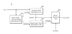
- FIG. 3 is a block diagram schematically illustrating the configuration of a clock signal generation circuit according to an embodiment.
- FIG. 4 is a block diagram schematically illustrating the configuration of the clock delay control signal generation unit illustrated in FIG. 3 .
- FIG. 5 is a diagram illustrating the configuration of the oscillator illustrated in FIG. 4 according an embodiment.
- FIG. 6 is a diagram illustrating the configuration of the clock decoding section illustrated in FIG. 4 according an embodiment.
- FIG. 7 is a diagram illustrating the configuration of the doubler clock generation unit illustrated in FIG. 3 according an embodiment.
- FIG. 8 is a diagram illustrating the configuration of the delay block illustrated in FIG. 7 according an embodiment.
- FIG. 9 is a diagram illustrating the configuration of another delay block illustrated in FIG. 7 according an embodiment.
- FIG. 3 is a block diagram schematically illustrating the configuration of a clock signal generation circuit according to an embodiment.
- a clock signal generation circuit 1 includes a clock delay control signal generation unit 100 , a doubler clock generation unit 200 , and a quadrupler clock generation unit 300 .
- the clock delay control signal generation unit 100 is configured to divide a clock signal CLK to generate a divided clock signal, and configured to generate a plurality of periodic signals for a half period of the divided clock signal.
- the clock delay control signal generation unit 100 is configured to generate first clock delay control signals T 1 ⁇ 0:8> and second clock delay control signals T 2 ⁇ 0:7> from the plurality of periodic signals. That is, the clock delay control signal generation unit 100 measures the period of the clock signal CLK and generates the first clock delay control signals T 1 ⁇ 0:8> and the second clock delay control signals T 2 ⁇ 0:7> according to the measurement result.
- the doubler clock generation unit 200 is configured to delay the clock signal CLK for a first time in response to the first clock delay control signals T 1 ⁇ 0:8> to generate a first delayed clock signal, and configured to generate a first output clock signal CLKDB in response to the clock signal CLK and the first delayed clock signal.
- the first time may be set to a half period of the high level of the clock signal CLK, that is, a 1 ⁇ 4 period of the clock signal CLK.
- the quadrupler clock generation unit 300 is configured to delay the clock signal CLK for a second time in response to the second clock delay control signals T 2 ⁇ 0:7> to generate a second delayed clock signal, and configured to generate a second output clock signal CLKQD in response to the first output clock signal CLKDB and the second delayed clock signal.
- the second time may be set to a half of the first time. That is, the second time may be set to a one-eighth (1 ⁇ 8) period of the clock signal CLK.
- the doubler clock generation unit 200 can generate the first output clock signal CLKDB with a half (1 ⁇ 2) period (a frequency twice as high as that) of the clock signal CLK, and the quadrupler clock generation unit 300 can generate the second output clock signal CLKQD with a 1 ⁇ 4 period (a frequency four times as high as that) of the clock signal CLK.
- the invention is not limited thereto. For example, it is possible to generate clock signals with various periods according to the configuration described in more detail below.
- the clock signal generation circuit 1 is configured to divide the clock signal CLK to generate the divided clock signal, and configured to generate the first output clock signal CLKDB and the second output clock signal CLKQD using the plurality of periodic signals generated only for the half period of the divided clock signal. Consequently, it is possible to reduce current consumption while generating the output clock signals with desired periods.
- the clock signal generation circuit 1 may further include a clock selection unit 400 .
- the clock selection unit 400 can output one of the first output clock signal CLKDB and the second output clock signal CLKQD as a final output clock signal CLK_OUT in response to a clock selection signal CLKSEL.
- the clock selection signal CLKSEL may use a test mode signal.
- FIG. 4 is a block diagram schematically illustrating the configuration of the clock delay control signal generation unit illustrated in FIG. 3 .
- the clock delay control signal generation unit 100 includes a clock division section 110 , an oscillator 120 , and a clock decoding section 130 .
- the clock division section 110 is configured to divide the clock signal CLK to generate a divided clock signal CLK 32 .
- the clock division section 110 can divide the clock signal CLK by 32 to generate the divided clock signal CLK 32 with a period that is 32 times as long as that of the clock signal CLK.
- the clock division section 110 may have a configuration in which five dividers for dividing input clock signals by 2 are connected in series to one another.
- the oscillator 120 is configured to receive the divided clock signal CLK 32 and generate a reference periodic signal OSC.
- the oscillator 120 receives the divided clock signal CLK 32 to generate the reference periodic signal OSC with a predetermined period, and generates the reference periodic signal OSC which is continuously toggled for a half period of the divided clock signal CLK 32 .
- the clock division section 110 and the oscillator 120 serve as a divided signal generation unit.
- the clock decoding section 130 is configured to receive the reference periodic signal OSC and generate a plurality of periodic signals from the reference periodic signal OSC.
- the clock decoding section 130 generates the first clock delay control signals T 1 ⁇ 0:8> and the second clock delay control signals T 2 ⁇ 0:7> from the plurality of periodic signals.
- the first clock delay control signals T 1 ⁇ 0:8> and the second clock delay control signals T 2 ⁇ 0:7> may be signals for designating the delay amount such that the clock signal received in the doubler clock generation unit 200 and the quadrupler clock generation unit 300 can be delayed for the first time and the second time.
- each of the first clock delay control signals T 1 ⁇ 0:8> and the second clock delay control signals T 2 ⁇ 0:7> includes a plurality of bits, it is possible to generate the second clock delay control signals T 2 ⁇ 0:7> by shifting the first clock delay control signals T 1 ⁇ 0:8>. Detailed description thereof will be given below.
- FIG. 5 is a diagram illustrating the configuration of the oscillator illustrated in FIG. 4 according the embodiment.
- the oscillator 120 includes four unit delays UD.
- the oscillator 120 can generate the reference periodic signal OSC continuously toggled through a loop formed through the four unit delays UD. For example, when the delay amount of the unit delay UD is set to 100 picoseconds, the period of the reference periodic signal OSC generated through the oscillator 120 is 800 picoseconds.
- the oscillator 120 Since the oscillator 120 is deactivated when the divided clock signal CLK 32 goes from a high level to a low level, the oscillator 120 can generate the reference periodic signal OSC during the high level interval of the divided clock signal CLK 32 ; i.e., during the half period of the divided clock signal CLK 32 .
- FIG. 6 is a diagram illustrating the configuration of the clock decoding section illustrated in FIG. 4 according the embodiment.
- the clock decoding section 130 includes a periodic signal division part 131 and a latch part 132 .
- the periodic signal division part 131 is configured to receive the reference periodic signal OSC and generate a plurality of periodic signals COSC ⁇ 0:8>.
- the periodic signal division part 131 can generate the plurality of periodic signals COSC ⁇ 0:8> by sequentially dividing the reference periodic signal OSC by 2.
- the periodic signal division part 131 can sequentially divide the reference periodic signal OSC by 2 to generate the plurality of periodic signals COSC ⁇ 0:8>.
- the periodic signal division part 131 has a configuration in which nine division portions are connected in series to one another.
- each division portion divides a reception signal by 2, it is possible to generate the plurality of periodic signals COSC ⁇ 0:8> with a period that is twice as long as that of the reception signal. Since the reference periodic signal OSC is generated for the half period of the divided clock signal CLK 32 , the plurality of periodic signals COSC ⁇ 0:8> are also generated for the half period of the divided clock signal CLK 32 .
- the latch part 132 is configured to store the levels of the plurality of periodic signals COSC ⁇ 0:8> at the time point at which the half period of the divided clock signal CLK 32 ends; i.e., at the time point at which the divided clock signal CLK 32 changes from the high level to the low level.
- the latch part 132 receives the plurality of periodic signals COSC ⁇ 0:8> and a divided clock pulse CLK 32 P to generate the first clock delay control signals T 1 ⁇ 0:8> and the second clock delay control signals T 2 ⁇ 0:7>.
- the divided clock pulse CLK 32 P may be generated at the time point at which the divided clock signal CLK 32 changes from the high level to the low level.
- the latch part 132 latches the levels of the plurality of periodic signals COSC ⁇ 0:8> in response to the divided clock pulse CLK 32 P generated from the divided clock signal CLK 32 , and stores the latched levels as code values.
- the stored code values are output as the first clock delay control signals T 1 ⁇ 0:8> and the second clock delay control signals T 2 ⁇ 0:7>.
- the second clock delay control signals T 2 ⁇ 0:7> are generated by shifting the first clock delay control signals T 1 ⁇ 0:8>.
- the second clock delay control signals T 2 ⁇ 0:7> may have code values of 1001101 obtained by shifting the bits of the first clock delay control signals T 1 ⁇ 0:8> rightward.
- the second time which corresponds to the delay amount of the quadrupler clock generation unit 300 , is 1 ⁇ 2 of the first time, which corresponds to the delay amount of the doubler clock generation unit 200 .
- the code values of the second clock delay control signals T 2 ⁇ 0:7> obtained by shifting the code values of the first clock delay control signals T 1 ⁇ 0:8> rightward correspond to 1 ⁇ 2 of the code values of the first clock delay control signals T 1 ⁇ 0:8>. Consequently, the first clock delay control signals T 1 ⁇ 0:8> and the second clock delay control signals T 2 ⁇ 0:7> can be used to decide the first time and the second time corresponding to 1 ⁇ 2 of the first time.
- the invention is not limited thereto.
- the first time designated by the first clock delay control signals T 1 ⁇ 0:8> and the shift scheme for generating the second clock delay control signals T 2 ⁇ 0:7> may be changed and modified according to the period of a clock signal to be generated. Consequently, the clock delay control signal generation unit 100 illustrated in FIGS. 4 to 6 can generate the first clock delay control signals T 1 ⁇ 0:8> and the second clock delay control signals T 2 ⁇ 0:7>, which vary depending on the period of the input clock signal CLK.
- FIG. 7 is a diagram schematically illustrating the configuration of the doubler clock generation unit illustrated in FIG. 3 according the embodiment.
- the doubler clock generation unit 200 includes a decoding section 210 , a doubler clock delay section 220 , and a clock mixing section 230 .
- the decoding section 210 is configured to receive the first clock delay control signals T 1 ⁇ 0:8>, decode the first clock delay control signals T 1 ⁇ 0:8>, and generate first delay decoding signals CNT 345 ⁇ 0:7>, CNT 67 ⁇ 0:4> and CNT 8 ⁇ 0:1>.
- the decoding section 210 includes the first to third decoders 211 to 213 .
- the first decoder 211 is configured to decode the fourth to sixth bits T 1 ⁇ 3:5> of the first clock delay control signal
- the second decoder 212 is configured to decode the seventh and eighth bits T 1 ⁇ 6:7> of the first clock delay control signal
- the third decoder 213 is configured to decode the ninth bit T 1 ⁇ 8> of the first clock delay control signal.
- the first to third bits T 1 ⁇ 0:2> of the first clock delay control signal are used as the first delay decoding signals without separate decoding. Consequently, it is possible to generate the first delay decoding signals T 1 ⁇ 0:2>, CNT 345 ⁇ 0:7>, CNT 67 ⁇ 0:3> and CNT 8 ⁇ 0:1>.
- the reason for using the first to third bits T 1 ⁇ 0:2> of the first clock delay control signal without decoding and decoding the fourth to ninth bits T 1 ⁇ 3:8> thereof is as follows.
- the fourth bit T 1 ⁇ 3> of the first clock delay control signal is generated from the divided signal COSC ⁇ 3> output from the fourth division portion illustrated in FIG. 6 . That is, the reference periodic signal OSC is divided four times to have a period that is sixteen times as long as that of the reference periodic signal OSC. Since the reference periodic signal OSC is generated from the four unit delays UD illustrated in FIG. 5 , the 16-times periodic signal COSC ⁇ 3> has a period corresponding to the 128 unit delay amount.
- the first time corresponds to a 1 ⁇ 4 period of the clock signal.
- the 128 unit delay amount of the 16-times periodic signal is divided by 4.
- the reference periodic signal OSC is generated from the divided clock signal CLK 32 . Since the divided clock signal CLK 32 is generated by dividing the clock signal CLK by 32 (that is, the divided clock signal CLK 32 has a period that is 32 times as long as that of the clock signal CLK), the remaining 32 unit delay amount of the 16-times periodic signal is divided by 32 again.
- the value of the fourth bit T 1 ⁇ 3> of the first clock delay control signal is a time corresponding to 1 unit delay amount.
- the value of the seventh bit T 1 ⁇ 6> of the first clock delay control signal is a time corresponding to 8 unit delay amount
- the value of the ninth bit of the first clock delay control signal is a time corresponding to 32 unit delay amount.
- the value of the first bit of the first clock delay control signal is to be a time corresponding to 1 ⁇ 8 unit delay amount. Therefore, when the bit values of the first delay decoding signals CNT 345 ⁇ 0:7> increase one by one, the corresponding difference is 1 unit delay amount. When the bit values of the first delay decoding signals CNT 67 ⁇ 0:3> increase, the corresponding difference is 8 unit delay amount.
- the above specific decoding scheme has been described. However, the invention is not limited thereto. For example, the configuration of the oscillator and the decoding scheme may be changed and modified according to the requirement of a designer and a user or applications.
- the doubler clock delay section 220 is configured to receive the first delay decoding signals CNT 345 ⁇ 0:7>, CNT 67 ⁇ 0:3> and CNT 8 ⁇ 0:1>, delay the clock signal CLK for the first time, and generate a first delayed clock signal CLKD.
- the doubler clock delay section 220 includes first to eighth delay blocks (DLY) 221 to 228 and a fine delay block 229 .
- the first to eighth delay blocks 221 to 228 are sequentially connected in series to one another, and include eight unit delays, respectively, which will be described in more detail with reference to FIG. 8 .
- Whether the first to seventh delay blocks 221 to 227 are activated is determined in units of blocks in response to the first delay decoding signals CNT 67 ⁇ 0:3> allocated thereto. Since the first delay decoding signals CNT 67 ⁇ 0:3> have the difference corresponding to the 8 unit delay amount whenever there occurs an increase in the values thereof, whether the delay blocks each including the eight unit delays are activated is determined in units of blocks. Whether the eight unit delays included in the eighth delay block 228 are activated is determined in response to the first delay decoding signals CNT 345 ⁇ 0:7> allocated thereto. Since the first delay decoding signals CNT 345 ⁇ 0:7> have the difference corresponding to the 1 unit delay amount whenever there occurs an increase in the values thereof, whether the eight unit delays constituting the eighth delay block are activated is determined.
- the fine delay block is configured to perform fine delay in response to the first delay decoding signals T 1 ⁇ 0:2> without decoding.
- the doubler clock generation unit 200 can delay the clock signal CLK for the first time in response to the first delay decoding signals CNT 345 ⁇ 0:7>, CNT 67 ⁇ 0:3> and CNT 8 ⁇ 0:1> and generate the first delayed clock signal CLKD.
- the clock mixing section 230 is configured to mix the clock signal CLK with the first delayed clock signal CLKD and generate the first output clock signal CLKDB.
- the clock mixing section 230 may include a phase mixer, and for example, include an exclusive OR gate which receives the clock signal CLK and the first delayed clock signal CLKD as input signals.
- FIG. 8 is a diagram illustrating the configuration of the second delay block illustrated in FIG. 7 according the embodiment. Since the first to seventh delay blocks 221 to 227 have configurations similar to one another, the second delay block 222 will be representatively described.
- the second delay block 222 is configured to receive the first delay decoding signals CNT 67 ⁇ 2> and CNT 8 ⁇ 1> and the clock signal CLK allocated thereto, and delay these signals.
- the second delay block 222 includes a first NOR gate NOR 1 , a first NAND gate ND 1 , and eight unit delays UD.
- the first NOR gate NOR 1 is configured to receive the allocated first delay decoding signals CNT 67 ⁇ 2> and CNT 8 ⁇ 1>.
- the first NAND gate ND 1 is configured to receive the output of the first NOR gate NOR 1 and the clock signal CLK.
- the first unit delay UD is configured to receive the output of the first NAND gate ND 1 and the output of the first delay block 221 .
- Each of the second to eighth unit delays UD is configured to receive and delay the output of a unit delay of a previous stage.
- the unit delay UD has a unit delay amount substantially equal to that of the unit delay UD constituting the oscillator 120 illustrated in FIG. 5 .
- the eighth unit delay UD is configured to output the final output to the delay block 223 of the next stage.
- the delay block 222 can receive and delay the clock signal CLK to generate the output only when the allocated first delay decoding signals CNT 67 ⁇ 2> and CNT 8 ⁇ 1> are input at a low level. In other cases, the delay block 222 can block the input of the clock signal CLK, delay the input, which is output from the delay block 221 of a previous stage, and generate the output.
- FIG. 9 is a diagram illustrating the configuration of the eighth delay block illustrated in FIG. 7 according the embodiment.
- the eighth delay block 228 includes a second NOR gate NOR 2 , second to eleventh NAND gates ND 2 to ND 11 , and eight unit delays UD.
- the second NOR gate NOR 2 is configured to receive the allocated first delay decoding signals CNT 67 ⁇ 0> and CNT 8 ⁇ 0>.
- the second NAND gate ND 2 is configured to receive the output of the second NOR gate NOR 2 and the clock signal CLK.
- the third NAND gate ND 3 is configured to receive the output of the second NAND gate ND 2 and the output of the seventh delay block 227 illustrated in FIG. 7 .
- the third NAND gate ND 3 generates an input signal IND, which is input to the eight unit delays UD.
- the delay block 228 can generate the input signal IND from the clock signal CLK. In other cases, the delay block 228 can generate the input signal IND from the output of the seventh delay block 227 illustrated in FIG. 7 .
- the fourth to eleventh NAND gates ND 4 to ND 11 are configured to designate unit delays to which the input signal IND is input. That is, the fourth to eleventh NAND gates ND 4 to ND 11 commonly receive the input signal IND, and receive the allocated first delay decoding signals CNT 345 ⁇ 0:7>, respectively.
- the doubler clock delay section 220 can simultaneously control four delay blocks (32 unit delay amount) in response to the first delay decoding signals CNT 8 ⁇ 0:1>, control one delay block (8 unit delay amount) in response to the first delay decoding signals CNT 67 ⁇ 0:3>, and individually control one unit delay (1 unit delay amount) in response to the first delay decoding signals CNT 345 ⁇ 0:7>.
- All unit delays UD constituting the doubler clock delay section 220 have a delay amount substantially equal to that of the unit delays UD constituting the oscillator 120 illustrated in FIG. 5 , as described above. Consequently, it is possible to set the delay amount of the first time for which the clock signal CLK should be delayed from the first clock delay control signals T 1 ⁇ 0:8> generated from the periodic signal OSC.
- the quadrupler clock generation unit 300 illustrated in FIG. 3 may have a configuration substantially equal to that of the doubler clock generation unit 200 . That is, the quadrupler clock generation unit 300 is substantially equal to the doubler clock generation unit 200 , except that signals to be decoded are the second clock delay control signals T 2 ⁇ 0:7> and the first output clock signal CLKDB generated from the doubler clock generation unit 200 is received instead of the clock signal CLK.
- the clock signal generation circuit can divide a clock signal to generate a divided clock signal, and measure a high level pulse width (that is, a half period) of the clock signal using a plurality of periodic signals generated for a half period of the divided clock signal. That is, the high level pulse width of the clock signal can be measured by measuring a high level interval of the divided clock signal, and the first output clock signal can be generated by assigning a delay amount corresponding to 1 ⁇ 2 of the pulse width of the clock signal to the clock signal.
- the second output clock signal can be generated by assigning a delay amount, which corresponds to 1 ⁇ 4 of the pulse width of the clock signal, to the first output clock signal using the shifting of code values.
- the configuration of the oscillator and the configuration of the delay section are changed and modified, thereby generating clock signals with various periods other than 1 ⁇ 2 or 1 ⁇ 4.
Abstract
Description
- The present application claims priority under 35 U.S.C. §119(a) to Korean Patent Application No. 10-2011-0029686, filed on Mar. 31, 2011, in the Korean Intellectual Property Office, which is incorporated herein by reference in its entirety as if set forth in full.
- 1. Technical Field
- Various embodiments of the present invention relate to clock signal generation circuits. In particular, certain embodiments relate to a clock signal generation circuit for generating a clock signal with a desired period from an input clock signal.
- 2. Related Art
- A semiconductor integrated circuit typically operates in synchronization with a clock signal. The clock signal may be input from outside of the semiconductor integrated circuit, or may be generated through a clock generator in the semiconductor integrated circuit. Since the semiconductor integrated circuit performs various operations, it is not possible to perform all operations using only one clock signal with a constant period. Therefore, a circuit for generating a clock signal with a desired period from a clock signal with a reference period is required.
-
FIG. 1 is a diagram schematically illustrating a configuration of a clock multiplier generally used. InFIG. 1 , the clock multiplier includes a delay Delay and an exclusive OR gate XOR. The delay Delay delays an input clock signal CLK_IN and the exclusive OR gate XOR performs an XOR operation on the input clock signal CLK_IN and the output A of the delay Delay to generate an output clock signal CLK_OUT. When the delay amount of the delay Delay is set to one-quarter (¼) of one period of the input clock signal CLK_IN, a phase difference of ninety degrees (90°) occurs between the input clock signal CLK_IN and the output A of the delay Delay. Consequently, it is possible to generate the output clock signal CLK_OUT with a frequency (a period of ½) that is twice as high as the frequency of the input clock signal CLK_IN through the operation of the exclusive OR gate XOR. -
FIG. 2 is a diagram schematically illustrating the configuration of another clock multiplier in the conventional art. InFIG. 2 , the clock multiplier includes anoscillator 10, acounter 20, and alogic circuit 30. Theoscillator 10 continuously generates a periodic signal OSC with a frequency higher than a frequency of an input clock signal CLK_IN. Thecounter 20 receives the input clock signal CLK_IN and counts the number of toggles of the periodic signal OSC for one period of the input clock signal CLK_IN. Thelogic circuit 30 receives the output of thecounter 20 and the periodic signal OSC. Thelogic circuit 30 continuously generates a clock signal with a pulse width corresponding to ½ of the counted value of thecounter 20 from the periodic signal OSC, thereby generating an output clock signal CLK_OUT with a frequency that is twice as high as the frequency of the input clock signal CLK_IN. - However, the clock multipliers in the conventional art have the following problems. The clock multiplier illustrated in
FIG. 1 has the simplest configuration. However, the duty ratio of the output clock signal may change significantly according to the amount and degree of delay. Furthermore, when the duty ratio of the input clock signal is not constant, jitter of the output clock signal may increase. - The clock multiplier illustrated in
FIG. 2 has an advantage of being capable of reducing a change in the phase and the duty ratio. However, current consumption may increase according to the continuous use of the oscillator and an increase in the frequency of the periodic signal, and the areas of the counter and the logic circuit may significantly increase according to the bits of the counter. - Accordingly, there is a need for an improved clock signal generation circuit capable of accurately and stably generating a clock signal with a desired period from an input clock signal.
- In one embodiment of the present invention, a clock signal generation circuit includes: a clock delay control signal generation unit configured to divide a clock signal to generate a divided clock signal, generate a plurality of periodic signals for a half period of the divided clock signal, and output clock delay control signals generated from the plurality of periodic signals; and a doubler clock generation unit configured to delay the clock signal in response to the clock delay control signals to generate a delayed clock signal, and generate an output clock signal in response to the clock signal and the delayed clock signal.
- In another embodiment of the present invention, a clock signal generation circuit includes: a clock delay control signal generation unit configured to divide a clock signal to generate a divided clock signal, generate a plurality of periodic signals for a half period of the divided clock signal, and output first and second clock delay control signals generated from the plurality of periodic signals; a doubler clock generation unit configured to delay the clock signal for a first time in response to the first clock delay control signals to generate a first delayed clock signal, and generate a first output clock signal in response to the clock signal and the first delayed clock signal; and a quadrupler clock generation unit configured to delay the first output clock signal for a second time in response to the second clock delay control signals to generate a second delayed clock signal, and generate a second output clock signal in response to the first output clock signal and the second delayed clock signal.
- In still another embodiment of the present invention, a clock signal generation circuit includes: a periodic signal generation unit configured to divide a clock signal and generate a reference periodic signal for a half period of a divided clock signal; a clock decoding section configured to divide the reference periodic signal to generate a plurality of periodic signals, and decode the plurality of periodic signals to generate clock delay control signals; and a doubler clock generation unit configured to generate an output clock signal in response to the clock delay control signals and the clock signal.
- In still another embodiment of the present invention, a clock signal generation circuit includes: a periodic signal generation unit configured to divide a clock signal and generate a reference periodic signal for a half period of a divided clock signal; a clock decoding section configured to divide the reference periodic signal to generate a plurality of periodic signals, and decode the plurality of periodic signals to generate first and second clock delay control signals; a doubler clock generation unit configured to generate a first output clock signal in response to the first delay control signals and the clock signal; and a quadrupler clock generation unit configured to generate a second output clock signal in response to the second clock delay control signals and the first output clock signal.
- Additional objects and advantages of the invention will be set forth in part in the description which follows, and in part will be obvious from the description, or may be learned by practice of the invention. The objects and advantages of the invention will be realized and attained by means of the elements and combinations particularly pointed out in the appended claims.
- It is to be understood that both the foregoing general description and the following detailed description are exemplary and explanatory only and are not restrictive of the invention, as claimed.
- The accompanying drawings, which are incorporated in and constitute a part of this specification, illustrate various embodiments consistent with the invention and, together with the description, serve to explain the principles of the invention.
-
FIG. 1 is a diagram schematically illustrating the configuration of a clock multiplier in the conventional art. -
FIG. 2 is a diagram schematically illustrating the configuration of another clock multiplier in the conventional art. -
FIG. 3 is a block diagram schematically illustrating the configuration of a clock signal generation circuit according to an embodiment. -
FIG. 4 is a block diagram schematically illustrating the configuration of the clock delay control signal generation unit illustrated inFIG. 3 . -
FIG. 5 is a diagram illustrating the configuration of the oscillator illustrated inFIG. 4 according an embodiment. -
FIG. 6 is a diagram illustrating the configuration of the clock decoding section illustrated inFIG. 4 according an embodiment. -
FIG. 7 is a diagram illustrating the configuration of the doubler clock generation unit illustrated inFIG. 3 according an embodiment. -
FIG. 8 is a diagram illustrating the configuration of the delay block illustrated inFIG. 7 according an embodiment. -
FIG. 9 is a diagram illustrating the configuration of another delay block illustrated inFIG. 7 according an embodiment. - Reference will now be made in detail to the exemplary embodiments consistent with the present disclosure, examples of which are illustrated in the accompanying drawings. Wherever possible, the same reference characters will be used throughout the drawings to refer to the same or like parts.
-
FIG. 3 is a block diagram schematically illustrating the configuration of a clock signal generation circuit according to an embodiment. InFIG. 3 , a clocksignal generation circuit 1 includes a clock delay controlsignal generation unit 100, a doublerclock generation unit 200, and a quadruplerclock generation unit 300. The clock delay controlsignal generation unit 100 is configured to divide a clock signal CLK to generate a divided clock signal, and configured to generate a plurality of periodic signals for a half period of the divided clock signal. Furthermore, the clock delay controlsignal generation unit 100 is configured to generate first clock delay control signals T1<0:8> and second clock delay control signals T2<0:7> from the plurality of periodic signals. That is, the clock delay controlsignal generation unit 100 measures the period of the clock signal CLK and generates the first clock delay control signals T1<0:8> and the second clock delay control signals T2<0:7> according to the measurement result. - The doubler
clock generation unit 200 is configured to delay the clock signal CLK for a first time in response to the first clock delay control signals T1<0:8> to generate a first delayed clock signal, and configured to generate a first output clock signal CLKDB in response to the clock signal CLK and the first delayed clock signal. For example, the first time may be set to a half period of the high level of the clock signal CLK, that is, a ¼ period of the clock signal CLK. - The quadrupler
clock generation unit 300 is configured to delay the clock signal CLK for a second time in response to the second clock delay control signals T2<0:7> to generate a second delayed clock signal, and configured to generate a second output clock signal CLKQD in response to the first output clock signal CLKDB and the second delayed clock signal. For example, the second time may be set to a half of the first time. That is, the second time may be set to a one-eighth (⅛) period of the clock signal CLK. Consequently, in the embodiment, the doublerclock generation unit 200 can generate the first output clock signal CLKDB with a half (½) period (a frequency twice as high as that) of the clock signal CLK, and the quadruplerclock generation unit 300 can generate the second output clock signal CLKQD with a ¼ period (a frequency four times as high as that) of the clock signal CLK. However, the invention is not limited thereto. For example, it is possible to generate clock signals with various periods according to the configuration described in more detail below. - The clock
signal generation circuit 1 according to the embodiment is configured to divide the clock signal CLK to generate the divided clock signal, and configured to generate the first output clock signal CLKDB and the second output clock signal CLKQD using the plurality of periodic signals generated only for the half period of the divided clock signal. Consequently, it is possible to reduce current consumption while generating the output clock signals with desired periods. - In
FIG. 3 , the clocksignal generation circuit 1 may further include aclock selection unit 400. Theclock selection unit 400 can output one of the first output clock signal CLKDB and the second output clock signal CLKQD as a final output clock signal CLK_OUT in response to a clock selection signal CLKSEL. For example, the clock selection signal CLKSEL may use a test mode signal. -
FIG. 4 is a block diagram schematically illustrating the configuration of the clock delay control signal generation unit illustrated inFIG. 3 . The clock delay controlsignal generation unit 100 includes aclock division section 110, anoscillator 120, and aclock decoding section 130. Theclock division section 110 is configured to divide the clock signal CLK to generate a divided clock signal CLK32. InFIG. 4 , theclock division section 110 can divide the clock signal CLK by 32 to generate the divided clock signal CLK32 with a period that is 32 times as long as that of the clock signal CLK. Theclock division section 110 may have a configuration in which five dividers for dividing input clock signals by 2 are connected in series to one another. - The
oscillator 120 is configured to receive the divided clock signal CLK32 and generate a reference periodic signal OSC. Theoscillator 120 receives the divided clock signal CLK32 to generate the reference periodic signal OSC with a predetermined period, and generates the reference periodic signal OSC which is continuously toggled for a half period of the divided clock signal CLK32. Theclock division section 110 and theoscillator 120 serve as a divided signal generation unit. - The
clock decoding section 130 is configured to receive the reference periodic signal OSC and generate a plurality of periodic signals from the reference periodic signal OSC. Theclock decoding section 130 generates the first clock delay control signals T1<0:8> and the second clock delay control signals T2<0:7> from the plurality of periodic signals. The first clock delay control signals T1<0:8> and the second clock delay control signals T2<0:7> may be signals for designating the delay amount such that the clock signal received in the doublerclock generation unit 200 and the quadruplerclock generation unit 300 can be delayed for the first time and the second time. When each of the first clock delay control signals T1<0:8> and the second clock delay control signals T2<0:7> includes a plurality of bits, it is possible to generate the second clock delay control signals T2<0:7> by shifting the first clock delay control signals T1<0:8>. Detailed description thereof will be given below. -
FIG. 5 is a diagram illustrating the configuration of the oscillator illustrated inFIG. 4 according the embodiment. InFIG. 5 , theoscillator 120 includes four unit delays UD. When the received divided clock signal CLK32 is at a high level, theoscillator 120 can generate the reference periodic signal OSC continuously toggled through a loop formed through the four unit delays UD. For example, when the delay amount of the unit delay UD is set to 100 picoseconds, the period of the reference periodic signal OSC generated through theoscillator 120 is 800 picoseconds. Since theoscillator 120 is deactivated when the divided clock signal CLK32 goes from a high level to a low level, theoscillator 120 can generate the reference periodic signal OSC during the high level interval of the divided clock signal CLK32; i.e., during the half period of the divided clock signal CLK32. -
FIG. 6 is a diagram illustrating the configuration of the clock decoding section illustrated inFIG. 4 according the embodiment. Theclock decoding section 130 includes a periodicsignal division part 131 and alatch part 132. The periodicsignal division part 131 is configured to receive the reference periodic signal OSC and generate a plurality of periodic signals COSC<0:8>. The periodicsignal division part 131 can generate the plurality of periodic signals COSC<0:8> by sequentially dividing the reference periodic signal OSC by 2. The periodicsignal division part 131 can sequentially divide the reference periodic signal OSC by 2 to generate the plurality of periodic signals COSC<0:8>. InFIG. 6 , the periodicsignal division part 131 has a configuration in which nine division portions are connected in series to one another. Since each division portion divides a reception signal by 2, it is possible to generate the plurality of periodic signals COSC<0:8> with a period that is twice as long as that of the reception signal. Since the reference periodic signal OSC is generated for the half period of the divided clock signal CLK32, the plurality of periodic signals COSC<0:8> are also generated for the half period of the divided clock signal CLK32. - The
latch part 132 is configured to store the levels of the plurality of periodic signals COSC<0:8> at the time point at which the half period of the divided clock signal CLK32 ends; i.e., at the time point at which the divided clock signal CLK32 changes from the high level to the low level. Thelatch part 132 receives the plurality of periodic signals COSC<0:8> and a divided clock pulse CLK32P to generate the first clock delay control signals T1<0:8> and the second clock delay control signals T2<0:7>. The divided clock pulse CLK32P may be generated at the time point at which the divided clock signal CLK32 changes from the high level to the low level. Thelatch part 132 latches the levels of the plurality of periodic signals COSC<0:8> in response to the divided clock pulse CLK32P generated from the divided clock signal CLK32, and stores the latched levels as code values. The stored code values are output as the first clock delay control signals T1<0:8> and the second clock delay control signals T2<0:7>. The second clock delay control signals T2<0:7> are generated by shifting the first clock delay control signals T1<0:8>. For example, when it is assumed that the first clock delay control signals T1<0:8> have code values of 10011010, the second clock delay control signals T2<0:7> may have code values of 1001101 obtained by shifting the bits of the first clock delay control signals T1<0:8> rightward. As described above, the second time, which corresponds to the delay amount of the quadruplerclock generation unit 300, is ½ of the first time, which corresponds to the delay amount of the doublerclock generation unit 200. Furthermore, the code values of the second clock delay control signals T2<0:7> obtained by shifting the code values of the first clock delay control signals T1<0:8> rightward correspond to ½ of the code values of the first clock delay control signals T1<0:8>. Consequently, the first clock delay control signals T1<0:8> and the second clock delay control signals T2<0:7> can be used to decide the first time and the second time corresponding to ½ of the first time. However, the invention is not limited thereto. For example, the first time designated by the first clock delay control signals T1<0:8> and the shift scheme for generating the second clock delay control signals T2<0:7> may be changed and modified according to the period of a clock signal to be generated. Consequently, the clock delay controlsignal generation unit 100 illustrated inFIGS. 4 to 6 can generate the first clock delay control signals T1<0:8> and the second clock delay control signals T2<0:7>, which vary depending on the period of the input clock signal CLK. -
FIG. 7 is a diagram schematically illustrating the configuration of the doubler clock generation unit illustrated inFIG. 3 according the embodiment. InFIG. 7 , the doublerclock generation unit 200 includes adecoding section 210, a doublerclock delay section 220, and aclock mixing section 230. Thedecoding section 210 is configured to receive the first clock delay control signals T1<0:8>, decode the first clock delay control signals T1<0:8>, and generate first delay decoding signals CNT345<0:7>, CNT67<0:4> and CNT8<0:1>. Thedecoding section 210 includes the first tothird decoders 211 to 213. Thefirst decoder 211 is configured to decode the fourth to sixth bits T1<3:5> of the first clock delay control signal, thesecond decoder 212 is configured to decode the seventh and eighth bits T1<6:7> of the first clock delay control signal, and thethird decoder 213 is configured to decode the ninth bit T1<8> of the first clock delay control signal. Meanwhile, the first to third bits T1<0:2> of the first clock delay control signal are used as the first delay decoding signals without separate decoding. Consequently, it is possible to generate the first delay decoding signals T1<0:2>, CNT345<0:7>, CNT67<0:3> and CNT8<0:1>. The reason for using the first to third bits T1<0:2> of the first clock delay control signal without decoding and decoding the fourth to ninth bits T1<3:8> thereof is as follows. The fourth bit T1<3> of the first clock delay control signal is generated from the divided signal COSC<3> output from the fourth division portion illustrated inFIG. 6 . That is, the reference periodic signal OSC is divided four times to have a period that is sixteen times as long as that of the reference periodic signal OSC. Since the reference periodic signal OSC is generated from the four unit delays UD illustrated inFIG. 5 , the 16-times periodic signal COSC<3> has a period corresponding to the 128 unit delay amount. - In the embodiment, the first time corresponds to a ¼ period of the clock signal. In this regard, the 128 unit delay amount of the 16-times periodic signal is divided by 4. Furthermore, the reference periodic signal OSC is generated from the divided clock signal CLK32. Since the divided clock signal CLK32 is generated by dividing the clock signal CLK by 32 (that is, the divided clock signal CLK32 has a period that is 32 times as long as that of the clock signal CLK), the remaining 32 unit delay amount of the 16-times periodic signal is divided by 32 again. According to the calculation result above, the value of the fourth bit T1<3> of the first clock delay control signal is a time corresponding to 1 unit delay amount. Through the above calculation, the value of the seventh bit T1<6> of the first clock delay control signal is a time corresponding to 8 unit delay amount, and the value of the ninth bit of the first clock delay control signal is a time corresponding to 32 unit delay amount. Furthermore, the value of the first bit of the first clock delay control signal is to be a time corresponding to ⅛ unit delay amount. Therefore, when the bit values of the first delay decoding signals CNT345<0:7> increase one by one, the corresponding difference is 1 unit delay amount. When the bit values of the first delay decoding signals CNT67<0:3> increase, the corresponding difference is 8 unit delay amount. In the embodiment, the above specific decoding scheme has been described. However, the invention is not limited thereto. For example, the configuration of the oscillator and the decoding scheme may be changed and modified according to the requirement of a designer and a user or applications.
- The doubler
clock delay section 220 is configured to receive the first delay decoding signals CNT345<0:7>, CNT67<0:3> and CNT8<0:1>, delay the clock signal CLK for the first time, and generate a first delayed clock signal CLKD. InFIG. 7 , the doublerclock delay section 220 includes first to eighth delay blocks (DLY) 221 to 228 and afine delay block 229. The first to eighth delay blocks 221 to 228 are sequentially connected in series to one another, and include eight unit delays, respectively, which will be described in more detail with reference toFIG. 8 . Whether the first to seventh delay blocks 221 to 227 are activated is determined in units of blocks in response to the first delay decoding signals CNT67<0:3> allocated thereto. Since the first delay decoding signals CNT67<0:3> have the difference corresponding to the 8 unit delay amount whenever there occurs an increase in the values thereof, whether the delay blocks each including the eight unit delays are activated is determined in units of blocks. Whether the eight unit delays included in theeighth delay block 228 are activated is determined in response to the first delay decoding signals CNT345<0:7> allocated thereto. Since the first delay decoding signals CNT345<0:7> have the difference corresponding to the 1 unit delay amount whenever there occurs an increase in the values thereof, whether the eight unit delays constituting the eighth delay block are activated is determined. - The fine delay block is configured to perform fine delay in response to the first delay decoding signals T1<0:2> without decoding. The doubler
clock generation unit 200 can delay the clock signal CLK for the first time in response to the first delay decoding signals CNT345<0:7>, CNT67<0:3> and CNT8<0:1> and generate the first delayed clock signal CLKD. - The
clock mixing section 230 is configured to mix the clock signal CLK with the first delayed clock signal CLKD and generate the first output clock signal CLKDB. Theclock mixing section 230 may include a phase mixer, and for example, include an exclusive OR gate which receives the clock signal CLK and the first delayed clock signal CLKD as input signals. -
FIG. 8 is a diagram illustrating the configuration of the second delay block illustrated inFIG. 7 according the embodiment. Since the first to seventh delay blocks 221 to 227 have configurations similar to one another, thesecond delay block 222 will be representatively described. Thesecond delay block 222 is configured to receive the first delay decoding signals CNT67<2> and CNT8<1> and the clock signal CLK allocated thereto, and delay these signals. Thesecond delay block 222 includes a first NOR gate NOR1, a first NAND gate ND1, and eight unit delays UD. The first NOR gate NOR1 is configured to receive the allocated first delay decoding signals CNT67<2> and CNT8<1>. The first NAND gate ND1 is configured to receive the output of the first NOR gate NOR1 and the clock signal CLK. The first unit delay UD is configured to receive the output of the first NAND gate ND1 and the output of thefirst delay block 221. Each of the second to eighth unit delays UD is configured to receive and delay the output of a unit delay of a previous stage. The unit delay UD has a unit delay amount substantially equal to that of the unit delay UD constituting theoscillator 120 illustrated inFIG. 5 . The eighth unit delay UD is configured to output the final output to thedelay block 223 of the next stage. Consequently, thedelay block 222 can receive and delay the clock signal CLK to generate the output only when the allocated first delay decoding signals CNT67<2> and CNT8<1> are input at a low level. In other cases, thedelay block 222 can block the input of the clock signal CLK, delay the input, which is output from thedelay block 221 of a previous stage, and generate the output. -
FIG. 9 is a diagram illustrating the configuration of the eighth delay block illustrated inFIG. 7 according the embodiment. InFIG. 9 , theeighth delay block 228 includes a second NOR gate NOR2, second to eleventh NAND gates ND2 to ND11, and eight unit delays UD. The second NOR gate NOR2 is configured to receive the allocated first delay decoding signals CNT67<0> and CNT8<0>. The second NAND gate ND2 is configured to receive the output of the second NOR gate NOR2 and the clock signal CLK. The third NAND gate ND3 is configured to receive the output of the second NAND gate ND2 and the output of theseventh delay block 227 illustrated inFIG. 7 . The third NAND gate ND3 generates an input signal IND, which is input to the eight unit delays UD. When the allocated first delay decoding signals CNT67<0> and CNT8<0> are at a low level, thedelay block 228 can generate the input signal IND from the clock signal CLK. In other cases, thedelay block 228 can generate the input signal IND from the output of theseventh delay block 227 illustrated inFIG. 7 . The fourth to eleventh NAND gates ND4 to ND11 are configured to designate unit delays to which the input signal IND is input. That is, the fourth to eleventh NAND gates ND4 to ND11 commonly receive the input signal IND, and receive the allocated first delay decoding signals CNT345<0:7>, respectively. Thus, only a NAND gate receiving a signal at a high level of the allocated first delay decoding signals CNT345<0:7> is activated to output the input signal IND. Consequently, unit delays designated by the fourth to eleventh NAND gates ND4 to ND11 can receive the input signal IND, and the input signal IND can be output after being sequentially delayed by unit delays of the next stages. That is, when the first delay decoding signals CNT345<0:5> are at a high level, the input signal IND can be input to the third unit delay, and the input signal IND can be output after being sequentially delayed six times. - Referring to
FIGS. 7 to 9 , it can be understood that the doublerclock delay section 220 can simultaneously control four delay blocks (32 unit delay amount) in response to the first delay decoding signals CNT8<0:1>, control one delay block (8 unit delay amount) in response to the first delay decoding signals CNT67<0:3>, and individually control one unit delay (1 unit delay amount) in response to the first delay decoding signals CNT345<0:7>. All unit delays UD constituting the doublerclock delay section 220 have a delay amount substantially equal to that of the unit delays UD constituting theoscillator 120 illustrated inFIG. 5 , as described above. Consequently, it is possible to set the delay amount of the first time for which the clock signal CLK should be delayed from the first clock delay control signals T1<0:8> generated from the periodic signal OSC. - The quadrupler
clock generation unit 300 illustrated inFIG. 3 may have a configuration substantially equal to that of the doublerclock generation unit 200. That is, the quadruplerclock generation unit 300 is substantially equal to the doublerclock generation unit 200, except that signals to be decoded are the second clock delay control signals T2<0:7> and the first output clock signal CLKDB generated from the doublerclock generation unit 200 is received instead of the clock signal CLK. - The clock signal generation circuit according to the embodiment can divide a clock signal to generate a divided clock signal, and measure a high level pulse width (that is, a half period) of the clock signal using a plurality of periodic signals generated for a half period of the divided clock signal. That is, the high level pulse width of the clock signal can be measured by measuring a high level interval of the divided clock signal, and the first output clock signal can be generated by assigning a delay amount corresponding to ½ of the pulse width of the clock signal to the clock signal. In addition, the second output clock signal can be generated by assigning a delay amount, which corresponds to ¼ of the pulse width of the clock signal, to the first output clock signal using the shifting of code values. Moreover, the configuration of the oscillator and the configuration of the delay section are changed and modified, thereby generating clock signals with various periods other than ½ or ¼.
- While certain embodiments have been described above, it will be understood to those skilled in the art that the embodiments described are by way of example only. Accordingly, the clock signal generation circuit described herein should not be limited based on the described embodiments. Rather, the clock signal generation circuit described herein should only be limited in light of the claims that follow when taken in conjunction with the above description and accompanying drawings.
Claims (29)
Applications Claiming Priority (2)
| Application Number | Priority Date | Filing Date | Title |
|---|---|---|---|
| KR10-2011-0029686 | 2011-03-31 | ||
| KR1020110029686A KR20120111282A (en) | 2011-03-31 | 2011-03-31 | Clock signal generating circuit |
Publications (2)
| Publication Number | Publication Date |
|---|---|
| US20120249201A1 true US20120249201A1 (en) | 2012-10-04 |
| US8514003B2 US8514003B2 (en) | 2013-08-20 |
Family
ID=46926393
Family Applications (1)
| Application Number | Title | Priority Date | Filing Date |
|---|---|---|---|
| US13/178,787 Active 2031-10-10 US8514003B2 (en) | 2011-03-31 | 2011-07-08 | Clock signal generation circuit |
Country Status (2)
| Country | Link |
|---|---|
| US (1) | US8514003B2 (en) |
| KR (1) | KR20120111282A (en) |
Cited By (1)
| Publication number | Priority date | Publication date | Assignee | Title |
|---|---|---|---|---|
| TWI585571B (en) * | 2016-11-04 | 2017-06-01 | 群聯電子股份有限公司 | Clock signal generation circuit, memory storage device and clock signal generation method |
Families Citing this family (2)
| Publication number | Priority date | Publication date | Assignee | Title |
|---|---|---|---|---|
| KR20160041318A (en) * | 2014-10-07 | 2016-04-18 | 에스케이하이닉스 주식회사 | Strobe signal interval detection circuit and memory system using the same |
| KR20220154482A (en) | 2021-05-13 | 2022-11-22 | 삼성전자주식회사 | Clock generating circuit and wireless communication device including the same |
Citations (4)
| Publication number | Priority date | Publication date | Assignee | Title |
|---|---|---|---|---|
| US5990715A (en) * | 1996-11-19 | 1999-11-23 | Fujitsu Limited | Semiconductor integrated circuit using a synchronized control signal |
| US6181174B1 (en) * | 1998-09-24 | 2001-01-30 | Fujitsu Limited | Semiconductor integrated circuit device |
| US7106114B2 (en) * | 2000-02-23 | 2006-09-12 | Fujitsu Limited | Delay time adjusting method of delaying a phase of an output signal until a phase difference between an input signal and the output signal becomes an integral number of periods other than zero |
| US7821311B2 (en) * | 2008-10-13 | 2010-10-26 | Hynix Semiconductor Inc. | Delay locked loop circuit and memory device having the same |
Family Cites Families (3)
| Publication number | Priority date | Publication date | Assignee | Title |
|---|---|---|---|---|
| KR100682182B1 (en) | 2004-04-12 | 2007-02-12 | 주식회사 하이닉스반도체 | Internal clock doubler and Semiconductor memory device having the same and data output method thereof |
| KR20090108178A (en) | 2008-04-11 | 2009-10-15 | 주식회사 하이닉스반도체 | Periodic pulse generator for high speed operation |
| KR101510777B1 (en) | 2009-03-20 | 2015-04-10 | 삼성전자주식회사 | Frequency measuring circuit and semiconductor device comprising the same |
-
2011
- 2011-03-31 KR KR1020110029686A patent/KR20120111282A/en active IP Right Grant
- 2011-07-08 US US13/178,787 patent/US8514003B2/en active Active
Patent Citations (4)
| Publication number | Priority date | Publication date | Assignee | Title |
|---|---|---|---|---|
| US5990715A (en) * | 1996-11-19 | 1999-11-23 | Fujitsu Limited | Semiconductor integrated circuit using a synchronized control signal |
| US6181174B1 (en) * | 1998-09-24 | 2001-01-30 | Fujitsu Limited | Semiconductor integrated circuit device |
| US7106114B2 (en) * | 2000-02-23 | 2006-09-12 | Fujitsu Limited | Delay time adjusting method of delaying a phase of an output signal until a phase difference between an input signal and the output signal becomes an integral number of periods other than zero |
| US7821311B2 (en) * | 2008-10-13 | 2010-10-26 | Hynix Semiconductor Inc. | Delay locked loop circuit and memory device having the same |
Cited By (1)
| Publication number | Priority date | Publication date | Assignee | Title |
|---|---|---|---|---|
| TWI585571B (en) * | 2016-11-04 | 2017-06-01 | 群聯電子股份有限公司 | Clock signal generation circuit, memory storage device and clock signal generation method |
Also Published As
| Publication number | Publication date |
|---|---|
| KR20120111282A (en) | 2012-10-10 |
| US8514003B2 (en) | 2013-08-20 |
Similar Documents
| Publication | Publication Date | Title |
|---|---|---|
| US10404262B2 (en) | Integrated circuit having a multiplying injection-locked oscillator | |
| US7224199B1 (en) | Circuit and method for digital delay and circuits incorporating the same | |
| KR102268767B1 (en) | Delay circuit and duty cycle controller including the same | |
| US20030020528A1 (en) | Clock controlling method and circuit | |
| JP4780144B2 (en) | Frequency divider circuit | |
| US9547475B2 (en) | Random number generating circuit | |
| JP5175697B2 (en) | DLL circuit and control method thereof | |
| US9647642B2 (en) | Clock phase adjustment mechanism of a ring oscillator using a phase control signal | |
| US11218141B2 (en) | Correction circuit | |
| JP2014039262A (en) | Initial phase variable ring oscillator | |
| US20090212833A1 (en) | Frequency divider circuit | |
| US8514003B2 (en) | Clock signal generation circuit | |
| US7812658B2 (en) | Clock generation circuit | |
| US7801263B2 (en) | Clock divider with a rational division factor | |
| US7424087B2 (en) | Clock divider | |
| US7952413B2 (en) | Clock generating circuit and clock generating method thereof | |
| CN110198162B (en) | Semiconductor device including clock generation circuit | |
| KR19980080163A (en) | Delay circuit | |
| US8319532B2 (en) | Frequency divider with phase selection functionality | |
| US10560053B2 (en) | Digital fractional frequency divider | |
| JP2009152886A (en) | Clock generating circuit and method of utilizing the same | |
| US8575972B2 (en) | Digital frequency synthesizer device and method thereof | |
| US10418982B2 (en) | Folded divider architecture | |
| US9081515B2 (en) | Clock generation circuit and clock generation system using the same | |
| JP2008271102A (en) | Ring oscillator and clock generating circuit |
Legal Events
| Date | Code | Title | Description |
|---|---|---|---|
| AS | Assignment |
Owner name: HYNIX SEMICONDUCTOR INC., KOREA, REPUBLIC OF Free format text: ASSIGNMENT OF ASSIGNORS INTEREST;ASSIGNOR:HONG, NAM PYO;REEL/FRAME:026562/0383 Effective date: 20110630 |
|
| STCF | Information on status: patent grant |
Free format text: PATENTED CASE |
|
| FEPP | Fee payment procedure |
Free format text: PAYOR NUMBER ASSIGNED (ORIGINAL EVENT CODE: ASPN); ENTITY STATUS OF PATENT OWNER: LARGE ENTITY |
|
| FPAY | Fee payment |
Year of fee payment: 4 |
|
| MAFP | Maintenance fee payment |
Free format text: PAYMENT OF MAINTENANCE FEE, 8TH YEAR, LARGE ENTITY (ORIGINAL EVENT CODE: M1552); ENTITY STATUS OF PATENT OWNER: LARGE ENTITY Year of fee payment: 8 |