US20120249306A1 - Rf-id tag and rf-id communication system - Google Patents
Rf-id tag and rf-id communication system Download PDFInfo
- Publication number
- US20120249306A1 US20120249306A1 US13/435,794 US201213435794A US2012249306A1 US 20120249306 A1 US20120249306 A1 US 20120249306A1 US 201213435794 A US201213435794 A US 201213435794A US 2012249306 A1 US2012249306 A1 US 2012249306A1
- Authority
- US
- United States
- Prior art keywords
- antenna
- loop
- booster antenna
- booster
- tag
- Prior art date
- Legal status (The legal status is an assumption and is not a legal conclusion. Google has not performed a legal analysis and makes no representation as to the accuracy of the status listed.)
- Abandoned
Links
Images


Classifications
-
- H—ELECTRICITY
- H01—ELECTRIC ELEMENTS
- H01Q—ANTENNAS, i.e. RADIO AERIALS
- H01Q1/00—Details of, or arrangements associated with, antennas
- H01Q1/36—Structural form of radiating elements, e.g. cone, spiral, umbrella; Particular materials used therewith
- H01Q1/38—Structural form of radiating elements, e.g. cone, spiral, umbrella; Particular materials used therewith formed by a conductive layer on an insulating support
-
- G—PHYSICS
- G06—COMPUTING; CALCULATING OR COUNTING
- G06K—GRAPHICAL DATA READING; PRESENTATION OF DATA; RECORD CARRIERS; HANDLING RECORD CARRIERS
- G06K19/00—Record carriers for use with machines and with at least a part designed to carry digital markings
- G06K19/06—Record carriers for use with machines and with at least a part designed to carry digital markings characterised by the kind of the digital marking, e.g. shape, nature, code
- G06K19/067—Record carriers with conductive marks, printed circuits or semiconductor circuit elements, e.g. credit or identity cards also with resonating or responding marks without active components
- G06K19/07—Record carriers with conductive marks, printed circuits or semiconductor circuit elements, e.g. credit or identity cards also with resonating or responding marks without active components with integrated circuit chips
- G06K19/077—Constructional details, e.g. mounting of circuits in the carrier
- G06K19/07749—Constructional details, e.g. mounting of circuits in the carrier the record carrier being capable of non-contact communication, e.g. constructional details of the antenna of a non-contact smart card
- G06K19/07766—Constructional details, e.g. mounting of circuits in the carrier the record carrier being capable of non-contact communication, e.g. constructional details of the antenna of a non-contact smart card comprising at least a second communication arrangement in addition to a first non-contact communication arrangement
- G06K19/07767—Constructional details, e.g. mounting of circuits in the carrier the record carrier being capable of non-contact communication, e.g. constructional details of the antenna of a non-contact smart card comprising at least a second communication arrangement in addition to a first non-contact communication arrangement the first and second communication means being two different antennas types, e.g. dipole and coil type, or two antennas of the same kind but operating at different frequencies
-
- G—PHYSICS
- G06—COMPUTING; CALCULATING OR COUNTING
- G06K—GRAPHICAL DATA READING; PRESENTATION OF DATA; RECORD CARRIERS; HANDLING RECORD CARRIERS
- G06K19/00—Record carriers for use with machines and with at least a part designed to carry digital markings
- G06K19/06—Record carriers for use with machines and with at least a part designed to carry digital markings characterised by the kind of the digital marking, e.g. shape, nature, code
- G06K19/067—Record carriers with conductive marks, printed circuits or semiconductor circuit elements, e.g. credit or identity cards also with resonating or responding marks without active components
- G06K19/07—Record carriers with conductive marks, printed circuits or semiconductor circuit elements, e.g. credit or identity cards also with resonating or responding marks without active components with integrated circuit chips
- G06K19/077—Constructional details, e.g. mounting of circuits in the carrier
- G06K19/07749—Constructional details, e.g. mounting of circuits in the carrier the record carrier being capable of non-contact communication, e.g. constructional details of the antenna of a non-contact smart card
- G06K19/07773—Antenna details
- G06K19/07777—Antenna details the antenna being of the inductive type
- G06K19/07779—Antenna details the antenna being of the inductive type the inductive antenna being a coil
- G06K19/07783—Antenna details the antenna being of the inductive type the inductive antenna being a coil the coil being planar
-
- G—PHYSICS
- G06—COMPUTING; CALCULATING OR COUNTING
- G06K—GRAPHICAL DATA READING; PRESENTATION OF DATA; RECORD CARRIERS; HANDLING RECORD CARRIERS
- G06K19/00—Record carriers for use with machines and with at least a part designed to carry digital markings
- G06K19/06—Record carriers for use with machines and with at least a part designed to carry digital markings characterised by the kind of the digital marking, e.g. shape, nature, code
- G06K19/067—Record carriers with conductive marks, printed circuits or semiconductor circuit elements, e.g. credit or identity cards also with resonating or responding marks without active components
- G06K19/07—Record carriers with conductive marks, printed circuits or semiconductor circuit elements, e.g. credit or identity cards also with resonating or responding marks without active components with integrated circuit chips
- G06K19/077—Constructional details, e.g. mounting of circuits in the carrier
- G06K19/07749—Constructional details, e.g. mounting of circuits in the carrier the record carrier being capable of non-contact communication, e.g. constructional details of the antenna of a non-contact smart card
- G06K19/07773—Antenna details
- G06K19/07786—Antenna details the antenna being of the HF type, such as a dipole
-
- G—PHYSICS
- G06—COMPUTING; CALCULATING OR COUNTING
- G06K—GRAPHICAL DATA READING; PRESENTATION OF DATA; RECORD CARRIERS; HANDLING RECORD CARRIERS
- G06K19/00—Record carriers for use with machines and with at least a part designed to carry digital markings
- G06K19/06—Record carriers for use with machines and with at least a part designed to carry digital markings characterised by the kind of the digital marking, e.g. shape, nature, code
- G06K19/067—Record carriers with conductive marks, printed circuits or semiconductor circuit elements, e.g. credit or identity cards also with resonating or responding marks without active components
- G06K19/07—Record carriers with conductive marks, printed circuits or semiconductor circuit elements, e.g. credit or identity cards also with resonating or responding marks without active components with integrated circuit chips
- G06K19/077—Constructional details, e.g. mounting of circuits in the carrier
- G06K19/07749—Constructional details, e.g. mounting of circuits in the carrier the record carrier being capable of non-contact communication, e.g. constructional details of the antenna of a non-contact smart card
- G06K19/07773—Antenna details
- G06K19/0779—Antenna details the antenna being foldable or folded
-
- G—PHYSICS
- G06—COMPUTING; CALCULATING OR COUNTING
- G06K—GRAPHICAL DATA READING; PRESENTATION OF DATA; RECORD CARRIERS; HANDLING RECORD CARRIERS
- G06K19/00—Record carriers for use with machines and with at least a part designed to carry digital markings
- G06K19/06—Record carriers for use with machines and with at least a part designed to carry digital markings characterised by the kind of the digital marking, e.g. shape, nature, code
- G06K19/067—Record carriers with conductive marks, printed circuits or semiconductor circuit elements, e.g. credit or identity cards also with resonating or responding marks without active components
- G06K19/07—Record carriers with conductive marks, printed circuits or semiconductor circuit elements, e.g. credit or identity cards also with resonating or responding marks without active components with integrated circuit chips
- G06K19/077—Constructional details, e.g. mounting of circuits in the carrier
- G06K19/07749—Constructional details, e.g. mounting of circuits in the carrier the record carrier being capable of non-contact communication, e.g. constructional details of the antenna of a non-contact smart card
- G06K19/07773—Antenna details
- G06K19/07794—Antenna details the record carrier comprising a booster or auxiliary antenna in addition to the antenna connected directly to the integrated circuit
-
- H—ELECTRICITY
- H01—ELECTRIC ELEMENTS
- H01Q—ANTENNAS, i.e. RADIO AERIALS
- H01Q1/00—Details of, or arrangements associated with, antennas
- H01Q1/12—Supports; Mounting means
- H01Q1/22—Supports; Mounting means by structural association with other equipment or articles
- H01Q1/2208—Supports; Mounting means by structural association with other equipment or articles associated with components used in interrogation type services, i.e. in systems for information exchange between an interrogator/reader and a tag/transponder, e.g. in Radio Frequency Identification [RFID] systems
- H01Q1/2225—Supports; Mounting means by structural association with other equipment or articles associated with components used in interrogation type services, i.e. in systems for information exchange between an interrogator/reader and a tag/transponder, e.g. in Radio Frequency Identification [RFID] systems used in active tags, i.e. provided with its own power source or in passive tags, i.e. deriving power from RF signal
-
- H—ELECTRICITY
- H01—ELECTRIC ELEMENTS
- H01Q—ANTENNAS, i.e. RADIO AERIALS
- H01Q19/00—Combinations of primary active antenna elements and units with secondary devices, e.g. with quasi-optical devices, for giving the antenna a desired directional characteristic
- H01Q19/22—Combinations of primary active antenna elements and units with secondary devices, e.g. with quasi-optical devices, for giving the antenna a desired directional characteristic using a secondary device in the form of a single substantially straight conductive element
-
- H—ELECTRICITY
- H01—ELECTRIC ELEMENTS
- H01Q—ANTENNAS, i.e. RADIO AERIALS
- H01Q7/00—Loop antennas with a substantially uniform current distribution around the loop and having a directional radiation pattern in a plane perpendicular to the plane of the loop
Definitions
- the present invention relates to an RF-ID (radio frequency identification) tag and an RF-ID communication system.
- non-contact communication devices which receive information from the outside and send information to the outside using electromagnetic waves as a medium have come to be used commonly (refer to JP-A-2006-203852 and JP-A-2009-075687, for example).
- a non-contact IC label and a non-contact card which are example non-contact communication devices are equipped with an IC chip and a communication antenna that is electrically connected to the IC chip.
- the communication antenna receives electromagnetic waves, electromotive force occurs in the communication antenna through resonance.
- the IC chip is activated by the electromotive force and information stored in the IC chip is converted into a signal.
- the signal representing the information is transmitted by the communication antenna and receivedby the antenna of a receiver.
- a controller of the receiver performs data processing such as signal identification.
- JP-A-2006-203852 discloses a non-contact IC module which is free of risk the function of a booster antenna is impaired.
- an IC chip is disposed at a position (the center of an antenna) where the current density of a dipole structure is highest.
- JP-A-2009-075687 discloses an RF-ID tag which is increased in the accuracy of communication with an external circuit and the degree of freedom of sticking.
- Non-contact communication devices as disclosed in JP-A-2006-203852 and JP-A-2009-075687 have a narrow resonance bandwidth because they are designed so as to perform a communication at a particular wavelength.
- the frequency of transmitted electromagnetic waves depends on the country, it is necessary to prepare communication antennas that are specialized for frequencies used in individual countries. Because of the narrow resonance bandwidth, allowable variation ranges of performance items of components such as an IC chip and antenna members are narrow, which may increase the cost and affect the stability of product operation.
- the resonance frequency may shift depending on the use situation such as interference between the communication antennas of adjoining RF-ID tags, which may disable a stable communication.
- a one-turn loop antenna is connected to an IC chip and a booster antenna is disposed close to the coil of the 1-turn loop antenna in non-contact form. And the 1-turn loop antenna is disposed at the center of the booster antenna. Since the IC chip is disposed close to (for example, mounted on) the 1-turn loop antenna, the IC chip is located approximately at the center of the booster antenna. Therefore, in printing a label on an RF-ID tag, printing on a label central portion is avoided to prevent the IC chip (located in the label central portion) from being damaged. This restriction inevitably lowers the value of label expression.
- the present invention has been made in the above circumstances, and a first object of the invention is to provide a configuration for increasing the bandwidth of a communication antenna of an RF-ID tag.
- a second object of the invention is to increase the degree of freedom of disposition of an IC chip by making it possible to dispose the IC chip at a position other than the center of a communication antenna.
- An RF-ID tag comprises an IC, a loop antenna to which the IC is connected, and a linear booster antenna which may be long and narrow as a whole, wherein:
- the booster antenna has, as one end portion in its longitudinal direction, a fold-back portion which is wound;
- a portion, having a length that measures 73% or more of a one-turn overall length of a loop of the loop antenna, of the loop antenna extends along a portion, including the fold-back portion, of the booster antenna.
- An RF-ID communication system comprises:
- a reader or a reader/writer which performs a wireless communication with the RF-ID tag.
- the RF-ID tag and the RF-ID communication system according to the invention make it possible to provide a configuration for increasing the bandwidth of a communication antenna and thereby contribute to cost reduction and stabilization of product operation. Furthermore, disposing an IC chip at a position other than the center of a communication antenna prevents a disconnection from occurring in a connection portion of the IC chip and an antenna portion and eliminates restrictions relating to label printing to avoid lowering of the value of label expression.
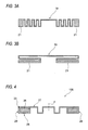
- FIG. 1 illustrates a dipole antenna and its current distribution.
- FIG. 2 shows the configuration of an RF-ID tag which is a combination of a loop antenna and a booster antenna.
- FIG. 3A shows a configuration in which a booster antenna has meandering structures extending in its longitudinal direction
- FIG. 3B shows a configuration in which a booster antenna has meandering structures extending in the direction that is perpendicular to its longitudinal direction.
- FIG. 4 shows the configuration of an RF-ID tag according to an embodiment of the present invention.
- FIG. 5 is an exploded view of part of the RF-ID tag of FIG. 4 .
- FIG. 6 shows a booster antenna model
- FIG. 7 shows other forms of a fold-back portion of the booster antenna.
- FIGS. 8A and 8B show models of booster antennas whose fold-back portions have different physical dimensions.
- FIG. 9A is a sectional view schematically showing a state that bending stress is imposed on a smart card in which a loop antenna and an IC chip are disposed at the center, in the longitudinal direction, of a booster antenna
- FIG. 9B is a sectional view schematically showing a state that bending stress is imposed on a smart card incorporating the RF-ID tag shown in FIG. 4 .
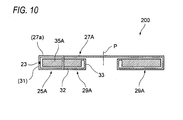
- FIG. 10 shows the configuration of an RF-ID tag according to another embodiment.
- FIGS. 11A and 11B show the configurations of RF-ID tags according to other embodiments.
- FIG. 12 is a schematic wiring diagram of an RF-ID tag system in which one of the RF-ID tags according to the embodiments is used as an active tag.
- FIG. 13 shows an appearance of a recording tape cartridge and a label stuck to it.
- FIG. 14 is a schematic diagram showing plural tape cartridges and a library apparatus.
- FIGS. 15A and 15B show analysis models having different positional relationships between a loop antenna and a booster antenna;
- FIG. 15A shows the configuration of a common antenna unit in which a loop antenna is disposed approximately at the center of a booster antenna, and
- FIG. 15B shows the configuration of an antenna unit in which a loop antenna is disposed at one end of a booster antenna.
- FIG. 16 is a graph showing simulation results of the S 11 parameter and the VSWR of each of the antenna units shown in FIGS. 15A and 15B .
- FIG. 17 shows an analysis model in which the position of a loop antenna is varied one end of a booster antenna to its center.
- FIG. 18 is a graph showing simulation results of the analysis model shown in FIG. 17 .
- FIGS. 19A , 19 B and 19 C show analysis models in which one end portion of a booster antenna coextends with two sides, three sides, and approximately four sides, respectively, of a loop antenna.
- FIG. 20 is a graph showing simulation results of the analysis model shown in FIGS. 19A , 19 B and 19 C.
- FIG. 21 shows an analysis model in which that portion of a loop antenna which coextends with one end portion of a booster antenna is varied between two sides and three sides.
- FIG. 22 is a graph showing simulation results of the analysis model shown in FIG. 21 .
- FIGS. 23A , 23 B and 23 C show analysis models in which a fold-back portion of a booster antenna has a spiral shape, a two-turn shape in which the inside loop and the outside loop are wound in opposite directions, and a shape in which a wide pad is formed inside a loop, respectively.
- FIG. 24 is a graph showing simulation results of the analysis model shown in FIGS. 23A , 23 B and 23 C.
- FIG. 25 shows an analysis model in which the length of a side including a projection, projecting from a loop antenna, of a fold-back portion of a booster antenna is varied.
- FIG. 26 is a graph showing simulation results of the analysis model shown in FIG. 25 .
- FIG. 28 shows an analysis model in which the length of a projection, projecting from a loop antenna, of a fold-back portion of a booster antenna is varied.
- FIG. 29 is a graph showing simulation results of the analysis model shown in FIG. 28 .
- FIG. 31 shows simulation results of the S 11 parameter and the VSWR of each of a one-turn loop antenna itself and a combination of a one-turn loop antenna and a booster antenna.
- FIG. 1 illustrates a dipole antenna and its current distribution.
- the dipole antenna 11 has a linear antenna portion 13 and an IC chip 15 which is disposed at the center, in the longitudinal direction, of the antenna portion 13 .
- the dipole antenna 11 has a current density distribution that the current density is low at both ends and high at the center.
- the loop antenna 17 is disposed at an end of the booster antenna 19 , the magnetic inductive coupling between the loop antenna 17 and the booster antenna 19 is insufficient and hence desired performance cannot be attained.
- the antenna length can be shortened by employing a meandering structure and the antenna length can be shortened further by adding wide pads 21 at both ends of an antenna.
- a dipole antenna etc. are designed taking into consideration impedance matching in a frequency band used.
- impedance matching in a frequency band used.
- UHF RF-ID tag antennas it is desired that their bandwidth be made as wide as possible because it is expected that they will be used being stuck to things made of various materials such as paper, plastics, and wood and hence they need to be designed so as to accommodate variations of permittivity values of these materials.
- the reflection coefficient S 11 parameter (reflection coefficient) and the VSWR (voltage standing wave ratio) are effective indices to be used for judging the level of bandwidth elongation. It is desirable that a dipole antenna or the like be designed so that the frequency range in which the S 11 parameter is smaller than or equal to ⁇ 3 dB or the VSWR is smaller than or equal to 6 (in general, smaller than or equal to 2) is wide.
- FIG. 4 shows the configuration of an RF-ID tag according to an embodiment of the invention.
- the RF-ID tag 100 is equipped with an IC chip 23 , a loop antenna 25 to which the IC chip 23 is connected, and a linear booster antenna (hereinafter referred to as a booster antenna) 27 which is long and narrow over its entire length.
- a booster antenna linear booster antenna
- FIG. 5 is an exploded view of part of the RF-ID tag 100 .
- the loop antenna 25 and the booster antenna 27 are formed separately and placed close to each other in non-contact form with a dielectric layer (not shown) interposed in between.
- the dielectric layer are an air layer, an adhesive layer, a printed circuit board, a plastic member made of polycarbonate or the like, and a ceramic member. It is preferable that the interval, in the thickness direction, between the loop antenna 25 and the booster antenna 27 be shorter than or equal to 2 mm.
- the loop antenna 25 is a rectangular-loop-shaped conductor, and the IC chip 23 is connected to (in electrical contact with) part of it.
- the loop antenna 25 is designed so as to have an optimum shape and size using its reflection coefficient S 11 , VSWR, and reverse transmission coefficient S 12 as indices so as to resonate in a UHF band around 900 MHz (850 MHz to 1 GHz).
- the loop antenna 25 may have a circular or polygonal shape.
- the IC chip 23 is located at a corner of the loop antenna 25 over one end, in the longitudinal direction, of the booster antenna 27 .
- the IC chip 23 may be located at any position in the loop antenna 25 and hence may be located, for example, on a side or at a corner.
- the booster antenna 27 has, as each end portion in its longitudinal direction, a fold-back portion 29 .
- Each fold-back portion 29 is wound in rectangular form and consists of a side 27 a which extends in the same direction as the longitudinal direction of the booster antenna 27 to the end in the longitudinal direction and three sides 31 - 33 which are wound from the end of the side 27 a (the side 31 is located at the end in the longitudinal direction of the booster antenna 27 ).
- One fold-back portion 29 extends along the loop antenna 25 .
- the sides of the loop antenna 25 coextend with at least three sides of the one fold-back portion 29 of the booster antenna 27 .
- approximately the four wound sides 27 a and 31 - 33 of the one fold-back portion 29 of the booster antenna 27 coextend with the sides of the loop antenna 25 .
- the sides 27 a and 31 - 33 of one fold-back portion 29 of the booster antenna 27 may extend close to the sides of the loop antenna 25 .
- the fold-back portion 29 of the booster antenna 27 may be wound in circular or polygonal form so as to conform to the shape of the loop antenna 25 .
- the overlap length should be greater than or equal to 73% (about 3 ⁇ 4) of the entire one-turn length of the loop antenna 25 .
- the overlap region is an arc region having a central angle 263°.
- the one-turn loop of the loop antenna 25 is square, the overlap region approximately corresponds to three sides.
- the booster antenna 27 is line-symmetrical with respect to a line P which passes through its center in its longitudinal direction and perpendicular to it.
- a pad 35 which is part of the fold-back portion 29 of the booster antenna 27 is disposed inside the loop of the loop antenna 25 .
- the booster antenna 19 exhibits somewhat different frequency characteristics when the fold-back portion 29 has a spiral form in which the inside loop is wound in the same direction as the outside loop and when the fold-back portion 29 has an oppositely wound form in which the winding direction of the inside loop is opposite to that of the outside loop. If the inside loop is replaced by a pad 35 having a pad surface, the booster antenna 19 is given a frequency characteristic that exhibits the frequency characteristics of both of the spiral form and the oppositely wound form. Whereas the fold-back portion 29 may be in either of the spiral form and the oppositely wound form, it is preferable that a loop-shaped pattern be formed around the outer circumference of a pad 35 .
- the booster antenna 27 may be made of any material having high conductivity, and may be formed by any of various forming methods such as a method of sticking, to a subject item, a metal sheet that has been worked into an antenna shape, evaporation or sputtering onto a subject item, printing using a conductive ink, and direct formation by etching.
- each of the loop antenna 25 and the booster antenna 27 is designed so as to resonate in a UHF band (850 MHz to 1 GHz), in the invention the resonance band is not limited to it.
- FIG. 6 shows a booster antenna model.
- a linear booster antenna 19 has a length that is a half of a wavelength ⁇ used. Therefore, in the embodiment, the above-described generally loop-shaped fold-back portion 29 to be electromagnetically coupled with the loop antenna 25 is disposed at one end, in the longitudinal direction, of the booster antenna 27 . It is appropriate to dispose the fold-back portion 29 in a ⁇ /6 region (extending from the end) of the booster antenna 27 . In other words, a loop to be electromagnetically coupled with the loop antenna 25 is formed in either of the end regions excluding the central ⁇ /6 region.
- wavelength ⁇ is a wavelength as converted using a current distribution and is not a physical dimension.
- FIGS. 8A and 8B show models of the fold-back portion 29 . As shown in FIGS. 8A and 8B , although the two booster antennas 19 have different total physical antenna lengths, both of them measure ⁇ /2 in terms of a current distribution. Current distribution differences occur only in the left-hand ⁇ /6 region of the booster antennas 19 . Therefore, the two booster antenna 19 have approximately the same antenna center position in terms of a current distribution (i.e., the antenna center position is not affected by the loop length of the fold-back portion 29 ).
- the loop antenna 25 is intentionally disposed at one end, in the longitudinal direction, of the booster antenna 27 where the current is small rather than at the center where the current is large and approximately the four sides of the loop antenna 25 are thereby coupled with the booster antenna 27 electromagnetically, whereby the communication-possible frequency band can be made wider while the communication sensitivity is kept sufficiently high.
- This makes it possible to use a single RF-ID tag to cover different frequencies used in individual countries.
- the increase in antenna bandwidth contributes to cost reduction and stabilization of product operation because allowable variation ranges of performance items of the IC chip 23 , antenna members, etc. are increased.
- the allowable range of resonance frequency variations that are caused by permittivity differences between goods havingRF-ID tags, interference between the antennas of many adjoining RF-ID tags, and environments (e.g., water contained in human bodies) of RF-ID tags.
- the resonance frequency can be adjusted by forming meandering lines in portions of the booster antenna 27 excluding the portion that overlaps with the loop antenna 25 .
- the IC chip 23 which is connected to the loop antenna 25 is disposed in the region that is not located at the center of the booster antenna 27 , occurrence of a disconnection in the connection portion of the IC chip 23 and the loop antenna 25 can be prevented when the RF-ID tag 100 is incorporated in a smart card.
- the disconnection preventing effect is enhanced by disposing the IC chip 23 at a position that is as close to the end, in the longitudinal direction, of the RF-ID tag 100 as possible.
- the smart card is a card such as a battery-less (i.e., no power source (battery) is provided) IC card, magnetic card, optical card, or a combination thereof which complies with ISO 7810, as typified by a smart cart incorporating a microprocessor and a memory.
- the smart card may also be a plastic card for an identification purpose only and like ones.
- FIG. 9A is a sectional view schematically showing a state that bending stress is imposed on a smart card 37 in which a loop antenna and an IC chip 15 are disposed at the center, in the longitudinal direction, of a booster antenna 19 .
- a connection portion of the IC chip 15 and the loop antenna is located in a region M where the bending stress is concentrated, a disconnection tends to be induced in the connection portion.
- FIG. 9B is a sectional view schematically showing a state that bending stress is imposed on a smart card 37 incorporating the RF-ID tag 100 shown in FIG. 4 .
- the IC chip 23 is not located in a region M where the bending stress is concentrated, the risk of occurrence of a disconnection in the connection portion of the IC chip 23 and the loop antenna 25 can be lowered.
- the IC chip 23 can be disposed at a label corner portion, as a result of which no restriction is imposed on label printing and the value of label expression is not lowered.
- RF-ID tag 100 In conventional, commonly employed antennas which are not designed so as to increase the bandwidth sufficiently, they are used in limited environments or countermeasures against influence of nearby objects (e.g., electronic components in general, water, a human body, and metal members) are taken such as addition of a radio wave absorbing sheet and formation of an ample internal space for reduction of influence.
- the RF-ID tag 100 shown in FIG. 4 makes it possible to relax such restrictions relating to the design.
- FIG. 10 shows the configuration of an RF-ID tag according to another embodiment.
- a fold-back portion 29 A is formed at both ends, in the longitudinal direction, of a booster antenna 27 A and a loop antenna 25 A is laid on one fold-back portion 29 A so as to overlap with the latter. That is, a side 27 a , a side 31 , and part of a side 32 of the booster antenna 27 A extend under (as viewed in FIG. 10 ) the loop antenna 25 A with a dielectric layer interposed in between.
- Each fold-back portion 29 A of the booster antenna 27 A is longer in the longitudinal direction than each fold-back portion 29 shown in FIG. 4 . More specifically, the side 32 and a pad 35 A of each fold-back portion 29 A is about two times as long as the side 32 and the pad 35 of each fold-back portion 29 shown in FIG. 4 .
- the portion other than the fold-back portions 29 A of the booster antenna 27 A is straight, and the entire booster antenna 27 A is line-symmetrical with respect to a center line P.
- the loop antenna 25 A has the same size as the loop antenna 25 shown in FIG. 4 , and an IC chip 23 is disposed on the loop antenna 25 A at a position that is right over the center of the side 31 (located at the end in the longitudinal direction) of the booster antenna 27 A.
- the antenna characteristics are improved by disposing the loop antenna 25 A over the end-side half of the fold-back portion 29 A which is longer than the loop antenna 25 A.
- FIG. 11A shows an RF-ID tag according to still another embodiment.
- the RF-ID tag 300 shown in FIG. 11A three sides of a loop antenna 25 B are electromagnetically coupled with a side 27 a , a side 31 , and part of a side 32 of a booster antenna 27 B and an IC chip 23 is disposed on the loop antenna 25 B at a position that is right over a corner of the side 31 (located at the end in the longitudinal direction) of the booster antenna 27 B.
- the resonance frequency can be decreased without increasing the width of the entire booster antenna 27 B because a pad 35 B of the booster antenna 27 B is disposed at such a position as not to be surrounded by the sides 27 a , 31 , and 32 .
- FIG. 11B shows an RF-ID tag according to yet another embodiment.
- approximately four sides of a loop antenna 25 C are electromagnetically coupled with sides 27 a and 31 - 33 of a booster antenna 27 C and an IC chip 23 is disposed on the loop antenna 25 C at a position that is right over a corner of the side 31 (located at the end in the longitudinal direction) of the booster antenna 27 C.
- the resonance frequency can be decreased without increasing the width of the entire booster antenna 27 C because a pad 35 C of the booster antenna 27 C is disposed at such a position as not to be surrounded by the sides 27 a and 31 - 33 .
- Each of the RF-ID tags 100 , 200 , 300 , and 400 according to the above embodiments can be used as not only a passive tag but also an active tag.
- the above-described advantages can also be obtained when each of the antenna configurations according to the above embodiments is applied to the antenna of a radio-type reader or a reader/writer.
- FIG. 12 shows the configuration of an RF-ID tag system in which one of the RF-ID tags 100 , 200 , 300 , and 400 according to the above embodiments is used as an active tag.
- FIG. 12 is a schematic wiring diagram of the RF-ID tag system.
- the RF-ID tag system 600 is equipped with an RF-ID tag antenna unit 500 , a receiving circuit 41 and a transmitting circuit 43 which are connected to the RF-ID tag antenna unit 500 , and a coupler 45 which splits a pair of signal lines coming from the RF-ID tag antenna unit 500 into two pairs of signal lines connected to the receiving circuit 41 and the transmitting circuit 43 , respectively.
- the RF-ID tag antenna unit 500 has a loop antenna 25 D and a booster antenna 27 D, and the loop antenna 25 D is connected to the receiving circuit 41 and the transmitting circuit 43 via the coupler 45 . That is, in this embodiment, the IC chip is replaced by the active tag communication system.
- each of the RF-ID tags 100 , 200 , 300 , and 400 can be applied to radio communication apparatus in general. More specifically, the following steps are taken. (1) A substrate with a loop antenna having a one-turn loop structure is manufactured and incorporated in an apparatus. (2) On the apparatus side, a booster antenna is disposed so as to have one of the above-describedpositional relationships with the one-turn loop antenna and to establish matching between them. In this case, the degree of freedom of the loop antenna position can be increased.
- a multilayer substrate two layers having an arbitrary interval is provided as a loop antenna forming layer and a booster antenna forming layer. Which layers a loop antenna and a booster antenna should be formed in is determined as appropriate taking into consideration the thickness of each layer of the substrate, the permittivity of the substrate, and the antenna shapes.
- a loop antenna is formed on a substrate which includes a power source for an active tag.
- a booster antenna is disposed on the inner surface or the outer surface of an apparatus case which houses the substrate, so as have a particular positional relationship with a loop antenna.
- the booster antenna can be attached and removed when necessary according to a use and whether to permit long-distance communication (security function) or a like item can be set.
- the one-turn loop antenna alone functions as a magnetic induction type tag.
- Example 1 Specific apparatus corresponding to the above Example 1 will be described below with reference to FIGS. 13 and 14 .
- FIG. 13 shows a recording tape cartridge 51 in which a magnetic tape T as an information recording medium is wound on a single reel 55 which is housed rotatably in a flat case 53 .
- a window 57 which is located in a headportion in the loading direction is opened and a leader member 59 which is provided at the head of the magnetic tape T is drawn out through the window 57 by the drive apparatus.
- the magnetic tape T is guided along a prescribed tape path in the drive apparatus and information is written to or read from the magnetic tape T.
- a label 65 is stuck to a label area in a recess of a back surface 61 (located on the origin side of arrow A) of the flat case 53 of the recording tape cartridge 51 . While not in use, the recording tape cartridge 51 is stored in a library apparatus with such orientation that the label 65 which is stuck to the label area 63 can be seen. Information represented by characters, symbols, etc. that can be seen by a user is printed or hand-written on the label 65 .
- An active or passive tag 67 including the receiving circuit 41 , the transmitting circuit 43 , the coupler 45 , and the loop antenna 25 D which are shown in FIG. 12 is provided in the recording tape cartridge 51 at a position that is close to the label area 63 .
- the booster antenna 27 D shown in FIG. 12 is formed in the label 65 .
- Information that was represented before by a bar code in the case of a bar code label for example, information for unified management of the individual cartridge 51 while it is stored or is being conveyedby an autoloader, and other information are stored in the receiving circuit 41 and the transmitting circuit 43 of the tag 67 or a storage unit (not shown) connected to them.
- a library apparatus which includes a holder for storing many recording tape cartridges 51 and an autoloader for automatically loading and removing a recording tape cartridge 51 into and from a drive apparatus.
- plural recording tape cartridges 51 are arranged at regular intervals in their thickness direction in a holder of a library apparatus 70 with such orientation that their labels 65 can be seen.
- a movable head 69 having a reader or a reader/writer is provided in the library apparatus 70 so as to be moved by a transport mechanism facing the labels 65 of the respective recording tape cartridges 51 which are arranged in the holder.
- the movable head 69 reads or writes information by performing a short-distance wireless (non-contact) communication with the booster antenna 27 D and the loop antenna 25 D of each recording tape cartridge 51 through a reader antenna or a reader/writer antenna as a communication antenna.
- the tag 67 can be disposed in a corner portion of the recording tape cartridge 51 , whereby a dead space can be utilized effectively and hence the efficiency of space utilization of the recording tape cartridge 51 can be made high.
- the tag 67 does not require printing, it is not necessary to provide, for example, a structure for preventing the IC chip from being damaged at the time of printing. Since the label 65 is provided with only the booster antenna 27 D, there are no restrictions relating to label printing and hence the value of label expression is not lowered. Since the dielectric layer which is the wall, interposed between the loop antenna 25 D and the booster antenna 27 D, of the case of the recording tape cartridge 51 can be as thick as about several millimeters, the degree of freedom of disposition of the loop antenna 25 D and the booster antenna 27 D is increased in the case where the loop antenna 25 D is disposed inside the recording tape cartridge 51 .
- the advantages of bandwidth increase are obtained, the risk of failure is lowered and the number of components and the cost of working can be decreased.
- the increase of a bandwidth used makes it possible to greatly relax the restrictions relating to the use conditions/environment of an RF-ID tag. For example, margins against influence of the permittivity of water contained in a sticking subject item (made of metal or plastics), a human body, or the like, interference between adjoining RF-ID tags, and other phenomena, whereby the quality of communication is made less prone to disturbances of a human body etc.
- this embodiment is advantageous when applied to tags with a wideband specification (worldwide specification).
- FIGS. 15A and 15B show analysis models having different positional relationships between a loop antenna 25 and a booster antenna 27 . More specifically, FIG. 15A shows the configuration of a common antenna unit in which a loop antenna 25 is disposed approximately at the center of a booster antenna 27 . FIG. 15B shows the configuration of an antenna unit in which a loop antenna 25 is disposed at one end of a booster antenna 27 .
- FIG. 16 is a graph showing simulation results of the S 11 parameter and the VSWR of each of the antenna units shown in FIGS. 15A and 15B .
- the left-hand vertical axis represents the S 11 parameter
- the right-hand vertical axis represents the VSWR
- the horizontal axis represents the frequency.
- a one-turn loop antenna 25 and a booster antenna 27 are formed on the respective surfaces of a 1-mm-thick dielectric layer made of a material having a permittivity 2.6.
- the loop antenna 25 has external dimensions 7.5 mm ⁇ 14 mm and a pattern width 1 mm.
- the booster antenna 27 has a basic pattern width 1 mm and its overall length is adjusted so that it has a resonance frequency 960 MHz.
- the minimum value of the S 11 parameter of the antenna unit of FIG. 15B in which a spiral fold-back portion is formed at one end of the booster antenna and the loop antenna 25 is laid on the fold-back portion is smaller than that of the antenna unit of FIG. 15A .
- the resonance bandwidths of the S 11 parameter and the VSWR of the antenna unit of FIG. 15B are wider than those of the antenna unit of FIG. 15A .
- FIG. 17 shows an analysis model in which the position of a loop antenna 25 is varied one end of a booster antenna 27 to its center.
- FIG. 18 shows analysis results. As the distance X decreases, that is, as the loop antenna 25 is moved from the center of the booster antenna 27 to its end, the minimum value of the S 11 parameter is increased and the resonance bandwidths of the S 11 parameter and the VSWR are reduced. The bandwidth reduction of each of the S 11 parameter and the VSWR is remarkable on the high frequency side.
- FIGS. 19A-19C show analysis models in which one end portion of a booster antenna 27 coextends with two sides, three sides, and four sides, respectively, of a loop antenna 25 .
- FIG. 20 shows analysis results. As the area of overlap between the one end portion of the booster antenna 27 and the loop antenna 25 increases, the minimum value of the S 11 parameter is made smaller and the resonance bandwidths of the S 11 parameter and the VSWR are increased.
- FIG. 21 shows an analysis model in which that portion of a loop antenna 25 which coextends with one end portion of a booster antenna 27 is varied between two sides and three sides. The entire overlap length is equal to the overlap length of the two sides plus a distance X.
- FIG. 22 shows simulation results.
- proportions of overlaps with the one end portion of the booster antenna 27 are also shown in percentage with respect to the overall length C (100%) of the one-turn loop antenna 25 .
- FIGS. 23A-23C show analysis models in which a fold-back portion 29 of a booster antenna 27 has a spiral shape of approximately two turns, a loop shape of approximately two turns in which the inside loop and the outside loop are wound in opposite directions, and a shape in which a wide pad 35 is formed inside a loop, respectively.
- FIG. 24 shows analysis results.
- the minimum value of the S 11 parameter is decreased and the resonance bandwidth of the S 11 parameter is increased in order of the oppositely wound shape, the spiral shape, and the pad-inclusive shape (the shape of the fold-back portion 29 ).
- the resonance bandwidth of the VSWR is also increased in the same order.
- FIG. 25 shows an analysis model in which the length of a side including a projection 71 , projecting from a loop antenna 25 , of a fold-back portion 29 of a booster antenna 27 is varied.
- the overall length L, in the longitudinal direction, of the booster antenna 27 was set in a range of 105 mm to 108 mm and the length X of the projection 71 was set at 0 mm, 6 mm, 26 mm, and 36 mm.
- FIG. 26 shows analysis results.
- the minimum value of the S 11 parameter is decreased as the length X varies from 0 mm to 6 mm, and is increased as the length X varies from 6 mm to 26 mm and then to 36 mm.
- the resonance bandwidth of the S 11 parameter is increased as the length X increases.
- the resonance bandwidth of the VSWR is increased as the length X increases.
- the resonance bandwidth is increased particularly on the high frequency side as the length X varies from 6 mm to 26 mm and then to 36 mm.
- FIGS. 27A and 27B show calculation results. It is seen that the resonance bandwidths of the S 11 parameter, the S 12 parameter, and the VSWR obtained when the length X is equal to 26 mm are greater than those obtained when length X is equal to 0 mm. It is concluded from the above analysis results that an optimum range of the length X is 26 mm to 36 mm.
- FIG. 28 shows an analysis model in which the length of a projection 73 , projecting from a loop antenna 25 , of a fold-back portion 29 of a booster antenna 27 is varied.
- the overall length L, in the longitudinal direction, of the booster antenna 27 was set in a range of 110 mm to 114 mm and the length X of the projection 73 was set at 0 mm, 10 mm, 30 mm, and 40 mm.
- FIG. 29 shows analysis results.
- the minimum value of the S 11 parameter is decreased as the length X varies from 0 mm to 10 mm, and is increased as the length X becomes 10 mm, 20 mm, 30 mm, and 40 mm in this order.
- the resonance bandwidth of the S 11 parameter is increased as the length X increases.
- the resonance bandwidth of the VSWR is increased as the length X increases.
- the resonance bandwidth is increased particularly on the high frequency side as the length X becomes 10 mm, 20 mm, 30 mm, and 40 mm in this order.
- FIGS. 30A and 30B show analysis results. It is seen that the resonance bandwidths of the S 11 parameter, the S 12 parameter, and the VSWR obtained when the length X is equal to 40 mm are greater than those obtained when length X is equal to 0 mm. The bandwidth increase of each parameter is remarkable on the high frequency side. It is concluded from the above analysis results that an optimum range of the length X is 30 mm to 40 mm.
- the resonance frequency of a one-turn loop antenna is determined by a combination of a capacitance component (C) of the IC chip and an inductance component (L) of the one-turn loop antenna.
- the inductance component the one-turn loop antenna mainly depends on the loop size, and a loop size is determined by an inductance component that conforms to a resonance frequency.
- the resistance component of the one-turn loop antenna is smaller than that of the IC chip and the VSWR is larger than 100, as a result of which matching is not attained.
- the booster antenna serves as a resistance component of the one-turn loop antenna.
- FIG. 31 shows calculation results of the S 11 parameter and the VSWR of each of a one-turn loop antenna itself and a combination of a one-turn loop antenna and a booster antenna.
- the VSWR of the one-turn loop antenna itself is equal to about 140
- An RF-ID tag comprising an IC, a loop antenna to which the IC is connected, and a linear booster antenna which may be long and narrow as a whole, wherein:
- the booster antenna has, as one end portion in its longitudinal direction, a fold-back portion which is wound;
- a portion, having a length that measures 73% or more of a one-turn overall length of a loop of the loop antenna, of the loop antenna extends along a portion, including the fold-back portion, of the booster antenna.
- each of the loop antenna and the booster antenna has a resonance frequency in a range of 850 MHz to 1 GHz.
- An RF-ID communication system comprising:
- a reader or a reader/writer which performs a wireless communication with the RF-ID tag.
Abstract
An RF-ID tag has an IC, a loop antenna to which the IC is connected, and a linear booster antenna, and the booster antenna has, as one end portion in a longitudinal direction of the linear booster antenna, a fold-back portion which is wound; and a portion, having a length that measures 73% or more of a one-turn overall length of a loop of the loop antenna, of the loop antenna extends along a portion, including the fold-back portion, of the booster antenna.
Description
- This application claims the benefit of Japanese Patent Application JP 2011-081056, filed Mar. 31, 2011, the entire content of which is hereby incorporated by reference, the same as if set forth at length.
- The present invention relates to an RF-ID (radio frequency identification) tag and an RF-ID communication system.
- In recent years, non-contact communication devices which receive information from the outside and send information to the outside using electromagnetic waves as a medium have come to be used commonly (refer to JP-A-2006-203852 and JP-A-2009-075687, for example). A non-contact IC label and a non-contact card which are example non-contact communication devices are equipped with an IC chip and a communication antenna that is electrically connected to the IC chip. When the communication antenna receives electromagnetic waves, electromotive force occurs in the communication antenna through resonance. The IC chip is activated by the electromotive force and information stored in the IC chip is converted into a signal. The signal representing the information is transmitted by the communication antenna and receivedby the antenna of a receiver. A controller of the receiver performs data processing such as signal identification.
- JP-A-2006-203852 discloses a non-contact IC module which is free of risk the function of a booster antenna is impaired. In this non-contact IC module, an IC chip is disposed at a position (the center of an antenna) where the current density of a dipole structure is highest. JP-A-2009-075687 discloses an RF-ID tag which is increased in the accuracy of communication with an external circuit and the degree of freedom of sticking.
- Non-contact communication devices as disclosed in JP-A-2006-203852 and JP-A-2009-075687 have a narrow resonance bandwidth because they are designed so as to perform a communication at a particular wavelength. However, since the frequency of transmitted electromagnetic waves depends on the country, it is necessary to prepare communication antennas that are specialized for frequencies used in individual countries. Because of the narrow resonance bandwidth, allowable variation ranges of performance items of components such as an IC chip and antenna members are narrow, which may increase the cost and affect the stability of product operation. Furthermore, the resonance frequency may shift depending on the use situation such as interference between the communication antennas of adjoining RF-ID tags, which may disable a stable communication.
- In general, a one-turn loop antenna is connected to an IC chip and a booster antenna is disposed close to the coil of the 1-turn loop antenna in non-contact form. And the 1-turn loop antenna is disposed at the center of the booster antenna. Since the IC chip is disposed close to (for example, mounted on) the 1-turn loop antenna, the IC chip is located approximately at the center of the booster antenna. Therefore, in printing a label on an RF-ID tag, printing on a label central portion is avoided to prevent the IC chip (located in the label central portion) from being damaged. This restriction inevitably lowers the value of label expression.
- The present invention has been made in the above circumstances, and a first object of the invention is to provide a configuration for increasing the bandwidth of a communication antenna of an RF-ID tag.
- A second object of the invention is to increase the degree of freedom of disposition of an IC chip by making it possible to dispose the IC chip at a position other than the center of a communication antenna.
- (1) An RF-ID tag according to the invention comprises an IC, a loop antenna to which the IC is connected, and a linear booster antenna which may be long and narrow as a whole, wherein:
- the booster antenna has, as one end portion in its longitudinal direction, a fold-back portion which is wound; and
- a portion, having a length that measures 73% or more of a one-turn overall length of a loop of the loop antenna, of the loop antenna extends along a portion, including the fold-back portion, of the booster antenna.
- (2) An RF-ID communication system according to the invention comprises:
- the RF-ID tag of item (1); and
- a reader or a reader/writer which performs a wireless communication with the RF-ID tag.
- The RF-ID tag and the RF-ID communication system according to the invention make it possible to provide a configuration for increasing the bandwidth of a communication antenna and thereby contribute to cost reduction and stabilization of product operation. Furthermore, disposing an IC chip at a position other than the center of a communication antenna prevents a disconnection from occurring in a connection portion of the IC chip and an antenna portion and eliminates restrictions relating to label printing to avoid lowering of the value of label expression.
-
FIG. 1 illustrates a dipole antenna and its current distribution. -
FIG. 2 shows the configuration of an RF-ID tag which is a combination of a loop antenna and a booster antenna. -
FIG. 3A shows a configuration in which a booster antenna has meandering structures extending in its longitudinal direction, andFIG. 3B shows a configuration in which a booster antenna has meandering structures extending in the direction that is perpendicular to its longitudinal direction. -
FIG. 4 shows the configuration of an RF-ID tag according to an embodiment of the present invention. -
FIG. 5 is an exploded view of part of the RF-ID tag ofFIG. 4 . -
FIG. 6 shows a booster antenna model. -
FIG. 7 shows other forms of a fold-back portion of the booster antenna. -
FIGS. 8A and 8B show models of booster antennas whose fold-back portions have different physical dimensions. -
FIG. 9A is a sectional view schematically showing a state that bending stress is imposed on a smart card in which a loop antenna and an IC chip are disposed at the center, in the longitudinal direction, of a booster antenna, andFIG. 9B is a sectional view schematically showing a state that bending stress is imposed on a smart card incorporating the RF-ID tag shown inFIG. 4 . -
FIG. 10 shows the configuration of an RF-ID tag according to another embodiment. -
FIGS. 11A and 11B show the configurations of RF-ID tags according to other embodiments. -
FIG. 12 is a schematic wiring diagram of an RF-ID tag system in which one of the RF-ID tags according to the embodiments is used as an active tag. -
FIG. 13 shows an appearance of a recording tape cartridge and a label stuck to it. -
FIG. 14 is a schematic diagram showing plural tape cartridges and a library apparatus. -
FIGS. 15A and 15B show analysis models having different positional relationships between a loop antenna and a booster antenna;FIG. 15A shows the configuration of a common antenna unit in which a loop antenna is disposed approximately at the center of a booster antenna, andFIG. 15B shows the configuration of an antenna unit in which a loop antenna is disposed at one end of a booster antenna. -
FIG. 16 is a graph showing simulation results of the S11 parameter and the VSWR of each of the antenna units shown inFIGS. 15A and 15B . -
FIG. 17 shows an analysis model in which the position of a loop antenna is varied one end of a booster antenna to its center. -
FIG. 18 is a graph showing simulation results of the analysis model shown inFIG. 17 . -
FIGS. 19A , 19B and 19C show analysis models in which one end portion of a booster antenna coextends with two sides, three sides, and approximately four sides, respectively, of a loop antenna. -
FIG. 20 is a graph showing simulation results of the analysis model shown inFIGS. 19A , 19B and 19C. -
FIG. 21 shows an analysis model in which that portion of a loop antenna which coextends with one end portion of a booster antenna is varied between two sides and three sides. -
FIG. 22 is a graph showing simulation results of the analysis model shown inFIG. 21 . -
FIGS. 23A , 23B and 23C show analysis models in which a fold-back portion of a booster antenna has a spiral shape, a two-turn shape in which the inside loop and the outside loop are wound in opposite directions, and a shape in which a wide pad is formed inside a loop, respectively. -
FIG. 24 is a graph showing simulation results of the analysis model shown inFIGS. 23A , 23B and 23C. -
FIG. 25 shows an analysis model in which the length of a side including a projection, projecting from a loop antenna, of a fold-back portion of a booster antenna is varied. -
FIG. 26 is a graph showing simulation results of the analysis model shown inFIG. 25 . -
FIG. 27A shows simulation results with a condition X=0 mm, andFIG. 27B shows simulation results with a condition X=26 mm. -
FIG. 28 shows an analysis model in which the length of a projection, projecting from a loop antenna, of a fold-back portion of a booster antenna is varied. -
FIG. 29 is a graph showing simulation results of the analysis model shown inFIG. 28 . -
FIG. 30A shows simulation results with a condition X=0 mm, andFIG. 30B shows simulation results with a condition X=40 mm. -
FIG. 31 shows simulation results of the S11 parameter and the VSWR of each of a one-turn loop antenna itself and a combination of a one-turn loop antenna and a booster antenna. -
- 13: Antenna portion
- 15: IC chip
- 17: Loop antenna
- 19: Booster antenna
- 21: Pad
- 23: IC chip
- 25, 25A: Loop antenna
- 27, 27A: Booster antenna (linear booster antenna)
- 27 a: Side
- 29, 29A: Fold-back portion
- 31, 32, 33: Side
- 35: Pad
- 37: Smart card
- 41: Receiving circuit
- 43: Transmitting circuit
- 51: Recording tape cartridge
- 65: Label
- 67: Tag
- 100, 200, 300, 400: RF-ID tag
- 600: RF-ID tag system
- Embodiments of the present invention will be hereinafter described in detail with reference to the drawings.
- First, a basic antenna configuration of an RF-ID tag and restrictions relating to antenna arrangement will be described briefly using a dipole antenna as an example.
-
FIG. 1 illustrates a dipole antenna and its current distribution. Thedipole antenna 11 has alinear antenna portion 13 and anIC chip 15 which is disposed at the center, in the longitudinal direction, of theantenna portion 13. Thedipole antenna 11 has a current density distribution that the current density is low at both ends and high at the center. - Therefore, when an RF-ID (radio frequency identification) tag is constructed by combining a
loop antenna 17 and abooster antenna 19 in a manner shown inFIG. 2 , maximum performance (maximum gain) is obtained by disposing theloop antenna 17 at the center of thebooster antenna 19. However, in this configuration, since thebooster antenna 19 is long in its longitudinal direction, the position where theloop antenna 17 is disposed is restricted to the center of thebooster antenna 19. - Usually, if the
loop antenna 17 is disposed at an end of thebooster antenna 19, the magnetic inductive coupling between theloop antenna 17 and thebooster antenna 19 is insufficient and hence desired performance cannot be attained. - As shown in
FIGS. 3A and 3B , the antenna length can be shortened by employing a meandering structure and the antenna length can be shortened further by addingwide pads 21 at both ends of an antenna. - Usually, a dipole antenna etc. are designed taking into consideration impedance matching in a frequency band used. However, in the case of UHF RF-ID tag antennas, it is desired that their bandwidth be made as wide as possible because it is expected that they will be used being stuck to things made of various materials such as paper, plastics, and wood and hence they need to be designed so as to accommodate variations of permittivity values of these materials.
- The reflection coefficient S11 parameter (reflection coefficient) and the VSWR (voltage standing wave ratio) are effective indices to be used for judging the level of bandwidth elongation. It is desirable that a dipole antenna or the like be designed so that the frequency range in which the S11 parameter is smaller than or equal to −3 dB or the VSWR is smaller than or equal to 6 (in general, smaller than or equal to 2) is wide.
-
FIG. 4 shows the configuration of an RF-ID tag according to an embodiment of the invention. The RF-ID tag 100 is equipped with anIC chip 23, aloop antenna 25 to which theIC chip 23 is connected, and a linear booster antenna (hereinafter referred to as a booster antenna) 27 which is long and narrow over its entire length. -
FIG. 5 is an exploded view of part of the RF-ID tag 100. As shown inFIG. 5 , theloop antenna 25 and thebooster antenna 27 are formed separately and placed close to each other in non-contact form with a dielectric layer (not shown) interposed in between. Examples of the dielectric layer are an air layer, an adhesive layer, a printed circuit board, a plastic member made of polycarbonate or the like, and a ceramic member. It is preferable that the interval, in the thickness direction, between theloop antenna 25 and thebooster antenna 27 be shorter than or equal to 2 mm. - The
loop antenna 25 is a rectangular-loop-shaped conductor, and theIC chip 23 is connected to (in electrical contact with) part of it. Theloop antenna 25 is designed so as to have an optimum shape and size using its reflection coefficient S11, VSWR, and reverse transmission coefficient S12 as indices so as to resonate in a UHF band around 900 MHz (850 MHz to 1 GHz). Alternatively, theloop antenna 25 may have a circular or polygonal shape. - In
FIG. 5 , theIC chip 23 is located at a corner of theloop antenna 25 over one end, in the longitudinal direction, of thebooster antenna 27. However, theIC chip 23 may be located at any position in theloop antenna 25 and hence may be located, for example, on a side or at a corner. - The
booster antenna 27 has, as each end portion in its longitudinal direction, a fold-back portion 29. Each fold-back portion 29 is wound in rectangular form and consists of aside 27 a which extends in the same direction as the longitudinal direction of thebooster antenna 27 to the end in the longitudinal direction and three sides 31-33 which are wound from the end of theside 27 a (theside 31 is located at the end in the longitudinal direction of the booster antenna 27). One fold-back portion 29 extends along theloop antenna 25. In the embodiment, the sides of theloop antenna 25 coextend with at least three sides of the one fold-back portion 29 of thebooster antenna 27. - In the example configuration of
FIG. 4 , approximately the fourwound sides 27 a and 31-33 of the one fold-back portion 29 of thebooster antenna 27 coextend with the sides of theloop antenna 25. Alternatively, thesides 27 a and 31-33 of one fold-back portion 29 of thebooster antenna 27 may extend close to the sides of theloop antenna 25. The fold-back portion 29 of thebooster antenna 27 may be wound in circular or polygonal form so as to conform to the shape of theloop antenna 25. - The overlap length should be greater than or equal to 73% (about ¾) of the entire one-turn length of the
loop antenna 25. Where the one-turn loop of theloop antenna 25 is circular, the overlap region is an arc region having a central angle 263°. Where the one-turn loop of theloop antenna 25 is square, the overlap region approximately corresponds to three sides. - The
booster antenna 27 is line-symmetrical with respect to a line P which passes through its center in its longitudinal direction and perpendicular to it. Apad 35 which is part of the fold-back portion 29 of thebooster antenna 27 is disposed inside the loop of theloop antenna 25. - As shown in the bottom part of
FIG. 7 , where the fold-back portion 29 of abooster antenna 19 is of two turns, thebooster antenna 19 exhibits somewhat different frequency characteristics when the fold-back portion 29 has a spiral form in which the inside loop is wound in the same direction as the outside loop and when the fold-back portion 29 has an oppositely wound form in which the winding direction of the inside loop is opposite to that of the outside loop. If the inside loop is replaced by apad 35 having a pad surface, thebooster antenna 19 is given a frequency characteristic that exhibits the frequency characteristics of both of the spiral form and the oppositely wound form. Whereas the fold-back portion 29 may be in either of the spiral form and the oppositely wound form, it is preferable that a loop-shaped pattern be formed around the outer circumference of apad 35. - The
booster antenna 27 may be made of any material having high conductivity, and may be formed by any of various forming methods such as a method of sticking, to a subject item, a metal sheet that has been worked into an antenna shape, evaporation or sputtering onto a subject item, printing using a conductive ink, and direct formation by etching. - Although in the embodiment each of the
loop antenna 25 and thebooster antenna 27 is designed so as to resonate in a UHF band (850 MHz to 1 GHz), in the invention the resonance band is not limited to it. -
FIG. 6 shows a booster antenna model. As shown inFIG. 6 , alinear booster antenna 19 has a length that is a half of a wavelength λ used. Therefore, in the embodiment, the above-described generally loop-shaped fold-back portion 29 to be electromagnetically coupled with theloop antenna 25 is disposed at one end, in the longitudinal direction, of thebooster antenna 27. It is appropriate to dispose the fold-back portion 29 in a λ/6 region (extending from the end) of thebooster antenna 27. In other words, a loop to be electromagnetically coupled with theloop antenna 25 is formed in either of the end regions excluding the central λ/6 region. - The term “wavelength λ” as used above is a wavelength as converted using a current distribution and is not a physical dimension.
FIGS. 8A and 8B show models of the fold-back portion 29. As shown inFIGS. 8A and 8B , although the twobooster antennas 19 have different total physical antenna lengths, both of them measure λ/2 in terms of a current distribution. Current distribution differences occur only in the left-hand λ/6 region of thebooster antennas 19. Therefore, the twobooster antenna 19 have approximately the same antenna center position in terms of a current distribution (i.e., the antenna center position is not affected by the loop length of the fold-back portion 29). - In the RF-
ID tag 100 shown inFIG. 4 , theloop antenna 25 is intentionally disposed at one end, in the longitudinal direction, of thebooster antenna 27 where the current is small rather than at the center where the current is large and approximately the four sides of theloop antenna 25 are thereby coupled with thebooster antenna 27 electromagnetically, whereby the communication-possible frequency band can be made wider while the communication sensitivity is kept sufficiently high. This makes it possible to use a single RF-ID tag to cover different frequencies used in individual countries. The increase in antenna bandwidth contributes to cost reduction and stabilization of product operation because allowable variation ranges of performance items of theIC chip 23, antenna members, etc. are increased. Furthermore, the allowable range of resonance frequency variations that are caused by permittivity differences between goods havingRF-ID tags, interference between the antennas of many adjoining RF-ID tags, and environments (e.g., water contained in human bodies) of RF-ID tags. - The resonance frequency can be adjusted by forming meandering lines in portions of the
booster antenna 27 excluding the portion that overlaps with theloop antenna 25. - Since the
IC chip 23 which is connected to theloop antenna 25 is disposed in the region that is not located at the center of thebooster antenna 27, occurrence of a disconnection in the connection portion of theIC chip 23 and theloop antenna 25 can be prevented when the RF-ID tag 100 is incorporated in a smart card. The disconnection preventing effect is enhanced by disposing theIC chip 23 at a position that is as close to the end, in the longitudinal direction, of the RF-ID tag 100 as possible. - The smart card is a card such as a battery-less (i.e., no power source (battery) is provided) IC card, magnetic card, optical card, or a combination thereof which complies with ISO 7810, as typified by a smart cart incorporating a microprocessor and a memory. The smart card may also be a plastic card for an identification purpose only and like ones.
-
FIG. 9A is a sectional view schematically showing a state that bending stress is imposed on asmart card 37 in which a loop antenna and anIC chip 15 are disposed at the center, in the longitudinal direction, of abooster antenna 19. In this case, since the connection portion of theIC chip 15 and the loop antenna is located in a region M where the bending stress is concentrated, a disconnection tends to be induced in the connection portion. -
FIG. 9B is a sectional view schematically showing a state that bending stress is imposed on asmart card 37 incorporating the RF-ID tag 100 shown inFIG. 4 . In this case, since theIC chip 23 is not located in a region M where the bending stress is concentrated, the risk of occurrence of a disconnection in the connection portion of theIC chip 23 and theloop antenna 25 can be lowered. - In the case of
FIG. 9A in which the loop antenna and theIC chip 15 are disposed at the center of thebooster antenna 19, in forming a label using the RF-ID tag, printing etc. on a label central portion needs to be avoided to prevent theIC chip 15 which is located there from being damaged. This restriction inevitably lowers the value of label expression. - On the other hand, in the case of
FIG. 9B in which theloop antenna 25 and theIC chip 23 are disposed at one end of thebooster antenna 27, theIC chip 23 can be disposed at a label corner portion, as a result of which no restriction is imposed on label printing and the value of label expression is not lowered. - In conventional, commonly employed antennas which are not designed so as to increase the bandwidth sufficiently, they are used in limited environments or countermeasures against influence of nearby objects (e.g., electronic components in general, water, a human body, and metal members) are taken such as addition of a radio wave absorbing sheet and formation of an ample internal space for reduction of influence. The RF-
ID tag 100 shown inFIG. 4 makes it possible to relax such restrictions relating to the design. - Next, an RF-ID tag according to another embodiment will be described.
FIG. 10 shows the configuration of an RF-ID tag according to another embodiment. In this RF-ID tag 200, as in the RF-ID tag 100 shown inFIG. 4 , a fold-back portion 29A is formed at both ends, in the longitudinal direction, of abooster antenna 27A and aloop antenna 25A is laid on one fold-back portion 29A so as to overlap with the latter. That is, aside 27 a, aside 31, and part of aside 32 of thebooster antenna 27A extend under (as viewed inFIG. 10 ) theloop antenna 25A with a dielectric layer interposed in between. - Each fold-
back portion 29A of thebooster antenna 27A is longer in the longitudinal direction than each fold-back portion 29 shown inFIG. 4 . More specifically, theside 32 and apad 35A of each fold-back portion 29A is about two times as long as theside 32 and thepad 35 of each fold-back portion 29 shown inFIG. 4 . The portion other than the fold-back portions 29A of thebooster antenna 27A is straight, and theentire booster antenna 27A is line-symmetrical with respect to a center line P. By elongating each fold-back portion 29A, the resonance frequency can be decreased without increasing the width of theentire booster antenna 27A. - The
loop antenna 25A has the same size as theloop antenna 25 shown inFIG. 4 , and anIC chip 23 is disposed on theloop antenna 25A at a position that is right over the center of the side 31 (located at the end in the longitudinal direction) of thebooster antenna 27A. - According to the RF-
ID tag 200 of this embodiment, the antenna characteristics are improved by disposing theloop antenna 25A over the end-side half of the fold-back portion 29A which is longer than theloop antenna 25A. -
FIG. 11A shows an RF-ID tag according to still another embodiment. In the RF-ID tag 300 shown inFIG. 11A , three sides of aloop antenna 25B are electromagnetically coupled with aside 27 a, aside 31, and part of aside 32 of abooster antenna 27B and anIC chip 23 is disposed on theloop antenna 25B at a position that is right over a corner of the side 31 (located at the end in the longitudinal direction) of thebooster antenna 27B. - According to the RF-
ID tag 300 of this embodiment, the resonance frequency can be decreased without increasing the width of theentire booster antenna 27B because apad 35B of thebooster antenna 27B is disposed at such a position as not to be surrounded by thesides -
FIG. 11B shows an RF-ID tag according to yet another embodiment. In the RF-ID tag 400 shown inFIG. 11B , approximately four sides of aloop antenna 25C are electromagnetically coupled withsides 27 a and 31-33 of abooster antenna 27C and anIC chip 23 is disposed on theloop antenna 25C at a position that is right over a corner of the side 31 (located at the end in the longitudinal direction) of thebooster antenna 27C. - According to the RF-
ID tag 400 of this embodiment, the resonance frequency can be decreased without increasing the width of theentire booster antenna 27C because apad 35C of thebooster antenna 27C is disposed at such a position as not to be surrounded by thesides 27 a and 31-33. - Each of the RF-
ID tags -
FIG. 12 shows the configuration of an RF-ID tag system in which one of the RF-ID tags FIG. 12 is a schematic wiring diagram of the RF-ID tag system. - The RF-
ID tag system 600 is equipped with an RF-IDtag antenna unit 500, a receivingcircuit 41 and a transmittingcircuit 43 which are connected to the RF-IDtag antenna unit 500, and acoupler 45 which splits a pair of signal lines coming from the RF-IDtag antenna unit 500 into two pairs of signal lines connected to the receivingcircuit 41 and the transmittingcircuit 43, respectively. - The RF-ID
tag antenna unit 500 has aloop antenna 25D and abooster antenna 27D, and theloop antenna 25D is connected to the receivingcircuit 41 and the transmittingcircuit 43 via thecoupler 45. That is, in this embodiment, the IC chip is replaced by the active tag communication system. - As is understood from the above description, each of the RF-
ID tags - In a multilayer substrate, two layers having an arbitrary interval is provided as a loop antenna forming layer and a booster antenna forming layer. Which layers a loop antenna and a booster antenna should be formed in is determined as appropriate taking into consideration the thickness of each layer of the substrate, the permittivity of the substrate, and the antenna shapes.
- A loop antenna is formed on a substrate which includes a power source for an active tag. A booster antenna is disposed on the inner surface or the outer surface of an apparatus case which houses the substrate, so as have a particular positional relationship with a loop antenna.
- Where as in the above examples the loop antenna and the booster antenna are separate from and not in contact with each other and have no wiring line connecting them, the booster antenna can be attached and removed when necessary according to a use and whether to permit long-distance communication (security function) or a like item can be set. In these examples, the one-turn loop antenna alone functions as a magnetic induction type tag.
- Specific apparatus corresponding to the above Example 1 will be described below with reference to
FIGS. 13 and 14 . -
FIG. 13 shows arecording tape cartridge 51 in which a magnetic tape T as an information recording medium is wound on asingle reel 55 which is housed rotatably in aflat case 53. When therecording tape cartridge 51 is loaded into a drive apparatus (not shown) in the direction indicated by arrow A, awindow 57 which is located in a headportion in the loading direction is opened and aleader member 59 which is provided at the head of the magnetic tape T is drawn out through thewindow 57 by the drive apparatus. The magnetic tape T is guided along a prescribed tape path in the drive apparatus and information is written to or read from the magnetic tape T. - A
label 65 is stuck to a label area in a recess of a back surface 61 (located on the origin side of arrow A) of theflat case 53 of therecording tape cartridge 51. While not in use, therecording tape cartridge 51 is stored in a library apparatus with such orientation that thelabel 65 which is stuck to thelabel area 63 can be seen. Information represented by characters, symbols, etc. that can be seen by a user is printed or hand-written on thelabel 65. - An active or
passive tag 67 including the receivingcircuit 41, the transmittingcircuit 43, thecoupler 45, and theloop antenna 25D which are shown inFIG. 12 is provided in therecording tape cartridge 51 at a position that is close to thelabel area 63. On the other hand, thebooster antenna 27D shown inFIG. 12 is formed in thelabel 65. When thelabel 65 is stuck to thelabel area 63, as described above the prescribed portion of thebooster antenna 27D overlaps with theloop antenna 25D with the wall of the case of therecording tape cartridge 51 interposed in between. - Information that was represented before by a bar code in the case of a bar code label, for example, information for unified management of the
individual cartridge 51 while it is stored or is being conveyedby an autoloader, and other information are stored in the receivingcircuit 41 and the transmittingcircuit 43 of thetag 67 or a storage unit (not shown) connected to them. - To use many
recording tape cartridges 51 as backup cartridges or the like, a library apparatus is used which includes a holder for storing manyrecording tape cartridges 51 and an autoloader for automatically loading and removing arecording tape cartridge 51 into and from a drive apparatus. As shown inFIG. 14 , pluralrecording tape cartridges 51 are arranged at regular intervals in their thickness direction in a holder of alibrary apparatus 70 with such orientation that theirlabels 65 can be seen. - A
movable head 69 having a reader or a reader/writer is provided in thelibrary apparatus 70 so as to be moved by a transport mechanism facing thelabels 65 of the respectiverecording tape cartridges 51 which are arranged in the holder. In thelibrary apparatus 70, while being moved in the arrangement direction of therecording tape cartridges 51, themovable head 69 reads or writes information by performing a short-distance wireless (non-contact) communication with thebooster antenna 27D and theloop antenna 25D of eachrecording tape cartridge 51 through a reader antenna or a reader/writer antenna as a communication antenna. - According to the RF-
ID tag system 600 shown inFIG. 12 , thetag 67 can be disposed in a corner portion of therecording tape cartridge 51, whereby a dead space can be utilized effectively and hence the efficiency of space utilization of therecording tape cartridge 51 can be made high. - Since the
tag 67 does not require printing, it is not necessary to provide, for example, a structure for preventing the IC chip from being damaged at the time of printing. Since thelabel 65 is provided with only thebooster antenna 27D, there are no restrictions relating to label printing and hence the value of label expression is not lowered. Since the dielectric layer which is the wall, interposed between theloop antenna 25D and thebooster antenna 27D, of the case of therecording tape cartridge 51 can be as thick as about several millimeters, the degree of freedom of disposition of theloop antenna 25D and thebooster antenna 27D is increased in the case where theloop antenna 25D is disposed inside therecording tape cartridge 51. - According to this embodiment, since no wiring line exists between the
loop antenna 25D and thebooster antenna 27D, no such failure as a disconnection or a contact failure is induced. In disassembling work of therecording tape cartridge 51, it is not necessary to conduct such appurtenant work as removal of screws or connector wires between the antennas. - Therefore, according to this embodiment, whereas the advantages of bandwidth increase are obtained, the risk of failure is lowered and the number of components and the cost of working can be decreased. The increase of a bandwidth used makes it possible to greatly relax the restrictions relating to the use conditions/environment of an RF-ID tag. For example, margins against influence of the permittivity of water contained in a sticking subject item (made of metal or plastics), a human body, or the like, interference between adjoining RF-ID tags, and other phenomena, whereby the quality of communication is made less prone to disturbances of a human body etc. Furthermore, this embodiment is advantageous when applied to tags with a wideband specification (worldwide specification).
- Next, a description will be made of simulation results of the antenna characteristics of the RF-ID tags according to the embodiments.
-
FIGS. 15A and 15B show analysis models having different positional relationships between aloop antenna 25 and abooster antenna 27. More specifically,FIG. 15A shows the configuration of a common antenna unit in which aloop antenna 25 is disposed approximately at the center of abooster antenna 27.FIG. 15B shows the configuration of an antenna unit in which aloop antenna 25 is disposed at one end of abooster antenna 27. -
FIG. 16 is a graph showing simulation results of the S11 parameter and the VSWR of each of the antenna units shown inFIGS. 15A and 15B . InFIG. 16 , the left-hand vertical axis represents the S11 parameter, the right-hand vertical axis represents the VSWR, and the horizontal axis represents the frequency. - In the models used in the simulation being discussed and simulations to be described later, a one-
turn loop antenna 25 and abooster antenna 27 are formed on the respective surfaces of a 1-mm-thick dielectric layer made of a material having a permittivity 2.6. Theloop antenna 25 has external dimensions 7.5 mm×14 mm and apattern width 1 mm. Thebooster antenna 27 has abasic pattern width 1 mm and its overall length is adjusted so that it has a resonance frequency 960 MHz. - As seen from
FIG. 16 , the minimum value of the S11 parameter of the antenna unit ofFIG. 15B in which a spiral fold-back portion is formed at one end of the booster antenna and theloop antenna 25 is laid on the fold-back portion is smaller than that of the antenna unit ofFIG. 15A . And the resonance bandwidths of the S11 parameter and the VSWR of the antenna unit ofFIG. 15B are wider than those of the antenna unit ofFIG. 15A . -
FIG. 17 shows an analysis model in which the position of aloop antenna 25 is varied one end of abooster antenna 27 to its center. -
FIG. 18 shows analysis results. As the distance X decreases, that is, as theloop antenna 25 is moved from the center of thebooster antenna 27 to its end, the minimum value of the S11 parameter is increased and the resonance bandwidths of the S11 parameter and the VSWR are reduced. The bandwidth reduction of each of the S11 parameter and the VSWR is remarkable on the high frequency side. These analysis results coincide with descriptions that are made in JP-A-2006-203852 and JP-A-2009-075687 as conditions for minimizing the S11 parameter. -
FIGS. 19A-19C show analysis models in which one end portion of abooster antenna 27 coextends with two sides, three sides, and four sides, respectively, of aloop antenna 25. -
FIG. 20 shows analysis results. As the area of overlap between the one end portion of thebooster antenna 27 and theloop antenna 25 increases, the minimum value of the S11 parameter is made smaller and the resonance bandwidths of the S11 parameter and the VSWR are increased. -
FIG. 21 shows an analysis model in which that portion of aloop antenna 25 which coextends with one end portion of abooster antenna 27 is varied between two sides and three sides. The entire overlap length is equal to the overlap length of the two sides plus a distance X. -
FIG. 22 shows simulation results. InFIG. 22 , proportions of overlaps with the one end portion of thebooster antenna 27 are also shown in percentage with respect to the overall length C (100%) of the one-turn loop antenna 25. It is seen fromFIG. 22 that it is preferable that the overlap length be greater than or equal to 73% of the overall length C of the one-turn loop antenna 25 (X=10 mm) because in that range the S11 parameter is smaller than −3 dB and the VSWR is smaller than 6. -
FIGS. 23A-23C show analysis models in which a fold-back portion 29 of abooster antenna 27 has a spiral shape of approximately two turns, a loop shape of approximately two turns in which the inside loop and the outside loop are wound in opposite directions, and a shape in which awide pad 35 is formed inside a loop, respectively. -
FIG. 24 shows analysis results. The minimum value of the S11 parameter is decreased and the resonance bandwidth of the S11 parameter is increased in order of the oppositely wound shape, the spiral shape, and the pad-inclusive shape (the shape of the fold-back portion 29). The resonance bandwidth of the VSWR is also increased in the same order. - (Analysis 5: Dependence on Shape of End Portion, Coextending with Three Sides of One-Turn Loop Antenna, of Booster Antenna)
-
FIG. 25 shows an analysis model in which the length of a side including aprojection 71, projecting from aloop antenna 25, of a fold-back portion 29 of abooster antenna 27 is varied. In this analysis, the overall length L, in the longitudinal direction, of thebooster antenna 27 was set in a range of 105 mm to 108 mm and the length X of theprojection 71 was set at 0 mm, 6 mm, 26 mm, and 36 mm. -
FIG. 26 shows analysis results. The minimum value of the S11 parameter is decreased as the length X varies from 0 mm to 6 mm, and is increased as the length X varies from 6 mm to 26 mm and then to 36 mm. The resonance bandwidth of the S11 parameter is increased as the length X increases. The resonance bandwidth of the VSWR is increased as the length X increases. The resonance bandwidth is increased particularly on the high frequency side as the length X varies from 6 mm to 26 mm and then to 36 mm. - To analyze the performance of communication between the antenna unit of the above analysis model and a reader/writer, values of the S12 parameter, the S12 parameter, and the VSWR were calculated under a condition that the antenna unit of the above analysis model and a wideband antenna (not shown) were opposed to each other with a distance 120 mm.
FIGS. 27A and 27B show calculation results. It is seen that the resonance bandwidths of the S11 parameter, the S12 parameter, and the VSWR obtained when the length X is equal to 26 mm are greater than those obtained when length X is equal to 0 mm. It is concluded from the above analysis results that an optimum range of the length X is 26 mm to 36 mm. - (Analysis 6: Dependence on Shape of End Portion, Coextending with Approximately Four Sides of One-Turn Loop Antenna, of Booster Antenna)
-
FIG. 28 shows an analysis model in which the length of aprojection 73, projecting from aloop antenna 25, of a fold-back portion 29 of abooster antenna 27 is varied. In this analysis, the overall length L, in the longitudinal direction, of thebooster antenna 27 was set in a range of 110 mm to 114 mm and the length X of theprojection 73 was set at 0 mm, 10 mm, 30 mm, and 40 mm. -
FIG. 29 shows analysis results. The minimum value of the S11 parameter is decreased as the length X varies from 0 mm to 10 mm, and is increased as the length X becomes 10 mm, 20 mm, 30 mm, and 40 mm in this order. The resonance bandwidth of the S11 parameter is increased as the length X increases. The resonance bandwidth of the VSWR is increased as the length X increases. The resonance bandwidth is increased particularly on the high frequency side as the length X becomes 10 mm, 20 mm, 30 mm, and 40 mm in this order. - The performance of communication between the antenna unit of the above analysis model and a reader/writer was analyzed.
-
FIGS. 30A and 30B show analysis results. It is seen that the resonance bandwidths of the S11 parameter, the S12 parameter, and the VSWR obtained when the length X is equal to 40 mm are greater than those obtained when length X is equal to 0 mm. The bandwidth increase of each parameter is remarkable on the high frequency side. It is concluded from the above analysis results that an optimum range of the length X is 30 mm to 40 mm. - Because of its simplest configuration, it is difficult to attain matching between a one-turn loop antenna and an IC chip on the market. The resonance frequency of a one-turn loop antenna is determined by a combination of a capacitance component (C) of the IC chip and an inductance component (L) of the one-turn loop antenna. The inductance component the one-turn loop antenna mainly depends on the loop size, and a loop size is determined by an inductance component that conforms to a resonance frequency. However, in this state, the resistance component of the one-turn loop antenna is smaller than that of the IC chip and the VSWR is larger than 100, as a result of which matching is not attained.
- On the other hand, if a one-turn loop antenna and a booster antenna are arranged so as to satisfy proper conditions, the booster antenna serves as a resistance component of the one-turn loop antenna. As a result, a combination of an IC chip and the unit consisting of the one-turn loop antenna and the booster antenna satisfies an impedance matching condition.
-
FIG. 31 shows calculation results of the S11 parameter and the VSWR of each of a one-turn loop antenna itself and a combination of a one-turn loop antenna and a booster antenna. Whereas the VSWR of the one-turn loop antenna itself is equal to about 140, the VSWR of the combination of the one-turn loop antenna and the booster antenna is smaller than 2 (seeFIG. 18 (X=54 mm). - The invention is not limited to the individual embodiments, and elements of different embodiments can be combined together. A person skilled in the art may be able to make modifications or applications on the basis of the disclosure of the specification and known techniques, and such modifications and applications should be covered by the scope to be protected.
- As described above, the following features are disclosed in the specification:
- (1) An RF-ID tag comprising an IC, a loop antenna to which the IC is connected, and a linear booster antenna which may be long and narrow as a whole, wherein:
- the booster antenna has, as one end portion in its longitudinal direction, a fold-back portion which is wound; and
- a portion, having a length that measures 73% or more of a one-turn overall length of a loop of the loop antenna, of the loop antenna extends along a portion, including the fold-back portion, of the booster antenna.
- (2) The RF-ID tag of item (1), wherein the loop antenna is laid on the fold-back portion of the booster antenna with a dielectric layer interposed in between.
- (3) The RF-ID tag of item (1) or (2), wherein the loop of the loop antenna has a circular or polygonal shape.
- (4) The RF-ID tag of item (3), wherein the fold-back portion of the booster antenna is wound in circular or polygonal form.
- (5) The RF-ID tag of any one of items (1) to (4), wherein the fold-back portion of the booster antenna is wound in rectangular form and at least three of four wound sides of the fold-back portion extend along sides of the loop antenna.
- (6) The RF-ID tag of any one of items (1) to (5), wherein the IC is disposed on the loop antenna at one end, in the longitudinal direction, of the booster antenna.
- (7) The RF-ID tag of any one of items (1) to (6), wherein the booster antenna is symmetrical with respect to a line that passes through a center, in the longitudinal direction, of the booster antenna and is perpendicular to the longitudinal direction.
- (8) The RF-ID tag of any one of items (1) to (7), wherein at least part of the fold-back portion of the booster antenna coextends with an inside portion that is located inside the loop of the loop antenna.
- (9) The RF-ID tag of any one of items (1) to (8), wherein the fold-back portion of the booster antenna is disposed in a region between one end, in the longitudinal direction, of the booster antenna and a position that is distant from the one end by ⅙ of a wavelength used.
- (10) The RF-ID tag of any one of items (1) to (9), wherein an insertion loss represented by an S11 parameter is smaller than or equal to −3 dB and a voltage standing wave ratio (VSWR) is smaller than or equal to 6.
- (11) The RF-ID tag of item (10), wherein each of the loop antenna and the booster antenna has a resonance frequency in a range of 850 MHz to 1 GHz.
- (12) The RF-ID tag of any one of items (1) to (11), wherein a portion, excluding the one end portion in the longitudinal direction, of the booster antenna has a meandering shape.
- (13) An RF-ID communication system comprising:
- the RF-ID tag of any one of items (1) to (12); and
- a reader or a reader/writer which performs a wireless communication with the RF-ID tag.
- Although the invention has been described above in relation to preferred embodiments and modifications thereof, it will be understood by those skilled in the art that other variations and modifications can be effected in these preferred embodiments without departing from the scope and spirit of the invention.
Claims (13)
1. An RF-ID tag comprising an IC, a loop antenna to which the IC is connected, and a linear booster antenna, wherein:
the booster antenna has, as one end portion in a longitudinal direction of the linear booster antenna, a fold-back portion which is wound; and
a portion, having a length that measures 73% or more of a one-turn overall length of a loop of the loop antenna, of the loop antenna extends along a portion, including the fold-back portion, of the booster antenna.
2. The RF-ID tag according to claim 1 , wherein the loop antenna is laid on the fold-back portion of the booster antenna with a dielectric layer interposed in between.
3. The RF-ID tag according to claim 1 , wherein the loop of the loop antenna has a circular or polygonal shape.
4. The RF-ID tag according to claim 3 , wherein the fold-back portion of the booster antenna is wound in circular or polygonal form.
5. The RF-ID tag according to claim 1 , wherein the fold-back portion of the booster antenna is wound in rectangular form and at least three of four wound sides of the fold-back portion extend along sides of the loop antenna.
6. The RF-ID tag according to claim 1 , wherein the IC is disposed on the loop antenna at one end, in the longitudinal direction, of the booster antenna.
7. The RF-ID tag according to claim 1 , wherein the booster antenna is symmetrical with respect to a line that passes through a center, in the longitudinal direction, of the booster antenna and is perpendicular to the longitudinal direction.
8. The RF-ID tag according to claim 1 , wherein at least part of the fold-back portion of the booster antenna coextends with an inside portion that is located inside the loop of the loop antenna.
9. The RF-ID tag according to claim 1 , wherein the fold-back portion of the booster antenna is disposed in a region between one end, in the longitudinal direction, of the booster antenna and a position that is distant from the one end by ⅙ of a wavelength used.
10. The RF-ID tag according to claim 1 , wherein an insertion loss represented by an S11 parameter is smaller than or equal to −3 dB and a voltage standing wave ratio is smaller than or equal to 6.
11. The RF-ID tag according to claim 10 , wherein each of the loop antenna and the booster antenna has a resonance frequency in a range of 850 MHz to 1 GHz.
12. The RF-ID tag according to claim 1 , wherein a portion, excluding the one end portion in the longitudinal direction, of the booster antenna has a meandering shape.
13. An RF-ID communication system comprising:
the RF-ID tag according to claim 1 ; and
a reader or a reader/writer which performs a wireless communication with the RF-ID tag.
Applications Claiming Priority (2)
| Application Number | Priority Date | Filing Date | Title |
|---|---|---|---|
| JP2011081056A JP5337834B2 (en) | 2011-03-31 | 2011-03-31 | RFID tag and RFID communication system |
| JP2011-081056 | 2011-03-31 |
Publications (1)
| Publication Number | Publication Date |
|---|---|
| US20120249306A1 true US20120249306A1 (en) | 2012-10-04 |
Family
ID=46926458
Family Applications (1)
| Application Number | Title | Priority Date | Filing Date |
|---|---|---|---|
| US13/435,794 Abandoned US20120249306A1 (en) | 2011-03-31 | 2012-03-30 | Rf-id tag and rf-id communication system |
Country Status (2)
| Country | Link |
|---|---|
| US (1) | US20120249306A1 (en) |
| JP (1) | JP5337834B2 (en) |
Cited By (10)
| Publication number | Priority date | Publication date | Assignee | Title |
|---|---|---|---|---|
| JP2014053686A (en) * | 2012-09-05 | 2014-03-20 | Nissei Ltd | Substrate type antenna |
| US20150339567A1 (en) * | 2012-11-29 | 2015-11-26 | Toppan Forms Co., Ltd. | Radio ic-mounted article, manufacturing method therefor, and management method for radio ic-mounted article |
| USD766881S1 (en) * | 2015-04-13 | 2016-09-20 | Megabyte Limited | RFID tag inlay |
| USD773442S1 (en) * | 2014-09-26 | 2016-12-06 | Megabyte Limited | RFID tag inlay |
| EP3163511A1 (en) * | 2015-10-26 | 2017-05-03 | Thomson Licensing | Multi-band rfid device |
| US20170236048A1 (en) * | 2014-10-30 | 2017-08-17 | Toppan Forms Co., Ltd. | Non-Contact Data Receiving/Transmitting Body |
| US10289944B2 (en) | 2015-07-08 | 2019-05-14 | Composecure, Llc | Metal smart card with dual interface capability |
| US10318859B2 (en) | 2015-07-08 | 2019-06-11 | Composecure, Llc | Dual interface metal smart card with booster antenna |
| WO2019136436A1 (en) * | 2018-01-08 | 2019-07-11 | Composecure, Llc | Dual interface metal smart card with booster antenna |
| CN114665259A (en) * | 2022-04-15 | 2022-06-24 | 合肥工业大学 | Ultra-wideband tag antenna suitable for metal liquid cross-coupling environment |
Families Citing this family (5)
| Publication number | Priority date | Publication date | Assignee | Title |
|---|---|---|---|---|
| JP5904287B2 (en) * | 2012-12-04 | 2016-04-13 | 日本電気株式会社 | Product management system |
| CN104078745A (en) * | 2013-03-29 | 2014-10-01 | 株式会社村田制作所 | Antenna assembly |
| WO2018045550A1 (en) * | 2016-09-09 | 2018-03-15 | Hong Kong R&D Centre for Logistics and Supply Chain Management Enabling Technologies Limited | A radio frequency communication device and a method for using thereof |
| WO2018147124A1 (en) * | 2017-02-10 | 2018-08-16 | 株式会社村田製作所 | Rfid-tagged article |
| JP7041872B2 (en) | 2017-10-30 | 2022-03-25 | 学校法人上智学院 | RFID tag and microwave oven heating container |
Citations (6)
| Publication number | Priority date | Publication date | Assignee | Title |
|---|---|---|---|---|
| US5198826A (en) * | 1989-09-22 | 1993-03-30 | Nippon Sheet Glass Co., Ltd. | Wide-band loop antenna with outer and inner loop conductors |
| US20060208900A1 (en) * | 2005-01-19 | 2006-09-21 | X-Ether, Inc. | Rfid antenna |
| US20060267138A1 (en) * | 2005-05-30 | 2006-11-30 | Semiconductor Energy Laboratory Co., Ltd. | Semiconductor device |
| US20070080890A1 (en) * | 2005-10-07 | 2007-04-12 | Chang-Fa Yang | Antenna apparatus |
| US20090160717A1 (en) * | 2007-12-19 | 2009-06-25 | Kabushiki Kaisha Toshiba | Antenna device and wireless device |
| US20100097280A1 (en) * | 2008-10-20 | 2010-04-22 | Smartrac Ip B.V. | Transponder device |
Family Cites Families (1)
| Publication number | Priority date | Publication date | Assignee | Title |
|---|---|---|---|---|
| CN102197537B (en) * | 2008-10-29 | 2014-06-18 | 株式会社村田制作所 | Wireless IC device |
-
2011
- 2011-03-31 JP JP2011081056A patent/JP5337834B2/en active Active
-
2012
- 2012-03-30 US US13/435,794 patent/US20120249306A1/en not_active Abandoned
Patent Citations (6)
| Publication number | Priority date | Publication date | Assignee | Title |
|---|---|---|---|---|
| US5198826A (en) * | 1989-09-22 | 1993-03-30 | Nippon Sheet Glass Co., Ltd. | Wide-band loop antenna with outer and inner loop conductors |
| US20060208900A1 (en) * | 2005-01-19 | 2006-09-21 | X-Ether, Inc. | Rfid antenna |
| US20060267138A1 (en) * | 2005-05-30 | 2006-11-30 | Semiconductor Energy Laboratory Co., Ltd. | Semiconductor device |
| US20070080890A1 (en) * | 2005-10-07 | 2007-04-12 | Chang-Fa Yang | Antenna apparatus |
| US20090160717A1 (en) * | 2007-12-19 | 2009-06-25 | Kabushiki Kaisha Toshiba | Antenna device and wireless device |
| US20100097280A1 (en) * | 2008-10-20 | 2010-04-22 | Smartrac Ip B.V. | Transponder device |
Cited By (16)
| Publication number | Priority date | Publication date | Assignee | Title |
|---|---|---|---|---|
| JP2014053686A (en) * | 2012-09-05 | 2014-03-20 | Nissei Ltd | Substrate type antenna |
| US20150339567A1 (en) * | 2012-11-29 | 2015-11-26 | Toppan Forms Co., Ltd. | Radio ic-mounted article, manufacturing method therefor, and management method for radio ic-mounted article |
| USD773442S1 (en) * | 2014-09-26 | 2016-12-06 | Megabyte Limited | RFID tag inlay |
| US10303994B2 (en) * | 2014-10-30 | 2019-05-28 | Toppan Forms Co., Ltd. | Non-contract data receiving/transmitting body |
| US20170236048A1 (en) * | 2014-10-30 | 2017-08-17 | Toppan Forms Co., Ltd. | Non-Contact Data Receiving/Transmitting Body |
| CN107112625A (en) * | 2014-10-30 | 2017-08-29 | 凸版资讯股份有限公司 | Noncontact data transmitter and receiver body |
| USD766881S1 (en) * | 2015-04-13 | 2016-09-20 | Megabyte Limited | RFID tag inlay |
| US10534990B2 (en) | 2015-07-08 | 2020-01-14 | Composecure, Llc | Metal smart card with dual interface capability |
| US10289944B2 (en) | 2015-07-08 | 2019-05-14 | Composecure, Llc | Metal smart card with dual interface capability |
| US10318859B2 (en) | 2015-07-08 | 2019-06-11 | Composecure, Llc | Dual interface metal smart card with booster antenna |
| US10748049B2 (en) | 2015-07-08 | 2020-08-18 | Composecure, Llc | Metal smart card with dual interface capability |
| US11301744B2 (en) | 2015-07-08 | 2022-04-12 | Composecure, Llc | Metal smart card with dual interface capability |
| US10038233B2 (en) | 2015-10-26 | 2018-07-31 | Thomson Licensing | Multi-band RFID device |
| EP3163511A1 (en) * | 2015-10-26 | 2017-05-03 | Thomson Licensing | Multi-band rfid device |
| WO2019136436A1 (en) * | 2018-01-08 | 2019-07-11 | Composecure, Llc | Dual interface metal smart card with booster antenna |
| CN114665259A (en) * | 2022-04-15 | 2022-06-24 | 合肥工业大学 | Ultra-wideband tag antenna suitable for metal liquid cross-coupling environment |
Also Published As
| Publication number | Publication date |
|---|---|
| JP5337834B2 (en) | 2013-11-06 |
| JP2012217042A (en) | 2012-11-08 |
Similar Documents
| Publication | Publication Date | Title |
|---|---|---|
| US20120249306A1 (en) | Rf-id tag and rf-id communication system | |
| JP4183707B2 (en) | Information processing apparatus including non-contact reader and / or writer, and coil antenna for magnetic coupling | |
| JP4803184B2 (en) | Coil antenna and portable electronic device | |
| CN102473244B (en) | Wireless IC tag, reader/writer, and information processing system | |
| US8004468B2 (en) | RIFD device with microstrip antennas | |
| US9016592B2 (en) | Antenna device and communication terminal apparatus | |
| US9024725B2 (en) | Communication terminal and information processing system | |
| JP5026522B2 (en) | Optimized reading method and system for transponders for high frequency communications using passive resonant circuits | |
| JP5429182B2 (en) | Wireless IC device | |
| JP5223584B2 (en) | Wireless communication device | |
| JP5176465B2 (en) | Non-contact IC tag and non-contact IC tag encoding method | |
| US20120119965A1 (en) | Transmission/reception antenna and transmission/reception device using same | |
| US8967487B2 (en) | Non-contact communication device | |
| WO2006078147A1 (en) | Thin rfid tag for radio frequency identification | |
| CN111931893B (en) | Radio frequency tag | |
| JP4873158B2 (en) | RFID reader device | |
| EP2453394A1 (en) | RF tag comprising a resonant circuit structure | |
| KR101321874B1 (en) | The nfc compact antenna module and rfid tag using thereof | |
| CN202854862U (en) | Electronic tag structure having selection and identification functions | |
| KR100867853B1 (en) | RFID antenna and RFID tag | |
| CN108320013B (en) | Omnidirectional RFID tag for metal surface and manufacturing method thereof | |
| KR100720614B1 (en) | Split wire dual resonance RFID tag antenna using open-loop slot | |
| WO2020026482A1 (en) | Rfid system and rack storage device with installed rfid tag | |
| CN103164733B (en) | A kind of Electronic Tag Structure with selective recognition function | |
| CN115332763A (en) | Folding ultrahigh frequency RFID double-sided anti-metal tag antenna |
Legal Events
| Date | Code | Title | Description |
|---|---|---|---|
| AS | Assignment |
Owner name: FUJIFILM CORPORATION, JAPAN Free format text: ASSIGNMENT OF ASSIGNORS INTEREST;ASSIGNOR:TADA, NOBUYUKI;REEL/FRAME:027965/0171 Effective date: 20120323 |
|
| STCB | Information on status: application discontinuation |
Free format text: ABANDONED -- FAILURE TO RESPOND TO AN OFFICE ACTION |