US20170123899A1 - Systems and Methods for Efficient Soft Data Based Flash Memory Data Recovery - Google Patents
Systems and Methods for Efficient Soft Data Based Flash Memory Data Recovery Download PDFInfo
- Publication number
- US20170123899A1 US20170123899A1 US14/925,714 US201514925714A US2017123899A1 US 20170123899 A1 US20170123899 A1 US 20170123899A1 US 201514925714 A US201514925714 A US 201514925714A US 2017123899 A1 US2017123899 A1 US 2017123899A1
- Authority
- US
- United States
- Prior art keywords
- binary
- soft data
- values
- data values
- yield
- Prior art date
- Legal status (The legal status is an assumption and is not a legal conclusion. Google has not performed a legal analysis and makes no representation as to the accuracy of the status listed.)
- Granted
Links
Images
Classifications
-
- G—PHYSICS
- G11—INFORMATION STORAGE
- G11C—STATIC STORES
- G11C16/00—Erasable programmable read-only memories
- G11C16/02—Erasable programmable read-only memories electrically programmable
- G11C16/06—Auxiliary circuits, e.g. for writing into memory
- G11C16/26—Sensing or reading circuits; Data output circuits
-
- G—PHYSICS
- G06—COMPUTING; CALCULATING OR COUNTING
- G06F—ELECTRIC DIGITAL DATA PROCESSING
- G06F11/00—Error detection; Error correction; Monitoring
- G06F11/07—Responding to the occurrence of a fault, e.g. fault tolerance
- G06F11/08—Error detection or correction by redundancy in data representation, e.g. by using checking codes
- G06F11/10—Adding special bits or symbols to the coded information, e.g. parity check, casting out 9's or 11's
- G06F11/1008—Adding special bits or symbols to the coded information, e.g. parity check, casting out 9's or 11's in individual solid state devices
- G06F11/1068—Adding special bits or symbols to the coded information, e.g. parity check, casting out 9's or 11's in individual solid state devices in sector programmable memories, e.g. flash disk
-
- G—PHYSICS
- G06—COMPUTING; CALCULATING OR COUNTING
- G06F—ELECTRIC DIGITAL DATA PROCESSING
- G06F11/00—Error detection; Error correction; Monitoring
- G06F11/07—Responding to the occurrence of a fault, e.g. fault tolerance
- G06F11/08—Error detection or correction by redundancy in data representation, e.g. by using checking codes
- G06F11/10—Adding special bits or symbols to the coded information, e.g. parity check, casting out 9's or 11's
- G06F11/1008—Adding special bits or symbols to the coded information, e.g. parity check, casting out 9's or 11's in individual solid state devices
- G06F11/1012—Adding special bits or symbols to the coded information, e.g. parity check, casting out 9's or 11's in individual solid state devices using codes or arrangements adapted for a specific type of error
-
- G—PHYSICS
- G11—INFORMATION STORAGE
- G11C—STATIC STORES
- G11C11/00—Digital stores characterised by the use of particular electric or magnetic storage elements; Storage elements therefor
- G11C11/56—Digital stores characterised by the use of particular electric or magnetic storage elements; Storage elements therefor using storage elements with more than two stable states represented by steps, e.g. of voltage, current, phase, frequency
- G11C11/5621—Digital stores characterised by the use of particular electric or magnetic storage elements; Storage elements therefor using storage elements with more than two stable states represented by steps, e.g. of voltage, current, phase, frequency using charge storage in a floating gate
- G11C11/5628—Programming or writing circuits; Data input circuits
-
- G—PHYSICS
- G11—INFORMATION STORAGE
- G11C—STATIC STORES
- G11C11/00—Digital stores characterised by the use of particular electric or magnetic storage elements; Storage elements therefor
- G11C11/56—Digital stores characterised by the use of particular electric or magnetic storage elements; Storage elements therefor using storage elements with more than two stable states represented by steps, e.g. of voltage, current, phase, frequency
- G11C11/5621—Digital stores characterised by the use of particular electric or magnetic storage elements; Storage elements therefor using storage elements with more than two stable states represented by steps, e.g. of voltage, current, phase, frequency using charge storage in a floating gate
- G11C11/5642—Sensing or reading circuits; Data output circuits
-
- G—PHYSICS
- G11—INFORMATION STORAGE
- G11C—STATIC STORES
- G11C16/00—Erasable programmable read-only memories
- G11C16/02—Erasable programmable read-only memories electrically programmable
- G11C16/06—Auxiliary circuits, e.g. for writing into memory
- G11C16/08—Address circuits; Decoders; Word-line control circuits
-
- G—PHYSICS
- G11—INFORMATION STORAGE
- G11C—STATIC STORES
- G11C16/00—Erasable programmable read-only memories
- G11C16/02—Erasable programmable read-only memories electrically programmable
- G11C16/06—Auxiliary circuits, e.g. for writing into memory
- G11C16/10—Programming or data input circuits
-
- G—PHYSICS
- G11—INFORMATION STORAGE
- G11C—STATIC STORES
- G11C29/00—Checking stores for correct operation ; Subsequent repair; Testing stores during standby or offline operation
- G11C29/52—Protection of memory contents; Detection of errors in memory contents
-
- G—PHYSICS
- G11—INFORMATION STORAGE
- G11C—STATIC STORES
- G11C7/00—Arrangements for writing information into, or reading information out from, a digital store
- G11C7/10—Input/output [I/O] data interface arrangements, e.g. I/O data control circuits, I/O data buffers
- G11C7/1006—Data managing, e.g. manipulating data before writing or reading out, data bus switches or control circuits therefor
-
- H—ELECTRICITY
- H03—ELECTRONIC CIRCUITRY
- H03M—CODING; DECODING; CODE CONVERSION IN GENERAL
- H03M13/00—Coding, decoding or code conversion, for error detection or error correction; Coding theory basic assumptions; Coding bounds; Error probability evaluation methods; Channel models; Simulation or testing of codes
- H03M13/03—Error detection or forward error correction by redundancy in data representation, i.e. code words containing more digits than the source words
- H03M13/05—Error detection or forward error correction by redundancy in data representation, i.e. code words containing more digits than the source words using block codes, i.e. a predetermined number of check bits joined to a predetermined number of information bits
- H03M13/11—Error detection or forward error correction by redundancy in data representation, i.e. code words containing more digits than the source words using block codes, i.e. a predetermined number of check bits joined to a predetermined number of information bits using multiple parity bits
- H03M13/1102—Codes on graphs and decoding on graphs, e.g. low-density parity check [LDPC] codes
- H03M13/1105—Decoding
- H03M13/1111—Soft-decision decoding, e.g. by means of message passing or belief propagation algorithms
-
- H—ELECTRICITY
- H03—ELECTRONIC CIRCUITRY
- H03M—CODING; DECODING; CODE CONVERSION IN GENERAL
- H03M13/00—Coding, decoding or code conversion, for error detection or error correction; Coding theory basic assumptions; Coding bounds; Error probability evaluation methods; Channel models; Simulation or testing of codes
- H03M13/63—Joint error correction and other techniques
- H03M13/6325—Error control coding in combination with demodulation
-
- H—ELECTRICITY
- H03—ELECTRONIC CIRCUITRY
- H03M—CODING; DECODING; CODE CONVERSION IN GENERAL
- H03M13/00—Coding, decoding or code conversion, for error detection or error correction; Coding theory basic assumptions; Coding bounds; Error probability evaluation methods; Channel models; Simulation or testing of codes
- H03M13/65—Purpose and implementation aspects
- H03M13/6577—Representation or format of variables, register sizes or word-lengths and quantization
- H03M13/6588—Compression or short representation of variables
-
- H—ELECTRICITY
- H03—ELECTRONIC CIRCUITRY
- H03M—CODING; DECODING; CODE CONVERSION IN GENERAL
- H03M5/00—Conversion of the form of the representation of individual digits
- H03M5/02—Conversion to or from representation by pulses
-
- H—ELECTRICITY
- H03—ELECTRONIC CIRCUITRY
- H03M—CODING; DECODING; CODE CONVERSION IN GENERAL
- H03M7/00—Conversion of a code where information is represented by a given sequence or number of digits to a code where the same, similar or subset of information is represented by a different sequence or number of digits
Definitions
- Embodiments are related to systems and methods for data storage, and more particularly to systems and methods for storing to and accessing data from a flash memory.
- multi-level cells are used. Such multi-level cells may be, for example, programmed to with one of four voltage levels with each of the four voltage levels representing a two bit binary value.
- a read back voltage is compared with a center voltage threshold to determine the least significant bit of the two bit binary value and additional comparisons are performed with an upper voltage threshold and a lower voltage threshold to determine the most significant bit of the two bit binary value.
- Use of multiple comparisons to yield the two bit binary value results in considerable latency.
- Embodiments are related to systems and methods for data storage, and more particularly to systems and methods for storing to and accessing data from a flash memory.
- FIG. 1 shows a solid state storage system including soft data output voltage value decoding circuitry in accordance with some embodiments of the present invention
- FIG. 2 shows an example of multi-level cell encoding using multiple low density parity check codewords in accordance with some embodiments of the present invention
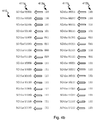
- FIG. 3 shows a five bit word to three voltage levels conversion table in accordance with some embodiments of the present invention
- FIG. 4 a shows another five bit word to three voltage levels conversion table in accordance with some embodiments of the present invention.
- FIGS. 4 b -4 d show page by page voltage level to corresponding bit(s) of the five bit word conversion in accordance with various embodiments of the present invention
- FIG. 5 shows a more detailed example of a solid state storage system including soft data output voltage value decoding circuitry in accordance with some embodiments of the present invention.
- FIG. 6 shows a method in accordance with various embodiments of the present invention for soft data based flash memory access.
- Embodiments are related to systems and methods for data storage, and more particularly to systems and methods for storing to and accessing data from a flash memory.
- Various embodiments of the present invention provide systems for accessing a flash memory device.
- the systems include: a data read circuit, a first data decoding circuit, and a second data decoding circuit.
- the data read circuit is operable to compare voltages read from a set of M groups of N flash memory cells with a first threshold value to yield a binary output set, where M and N are integers.
- the binary output set includes a set of M groups of N binary values.
- the first data decoding circuit is operable to generate at least a first set of M soft data values each corresponding to a respective one of the M groups of N binary values.
- the second data decoding circuit operable to decode the first set of M soft data values to yield a data output.
- the system is implemented as part of an integrated circuit.
- the first set of M soft data values corresponds to a low density parity check codeword
- the second data decoding circuit is a low density parity check decoding circuit.
- the binary output set is a first binary output set
- the data read circuit is further operable to compare voltages read from the set of M groups of N flash memory cells with a second threshold value to yield a second binary output set.
- the first data decoding circuit is further operable to generate at least a second set of M soft data values each corresponding to a respective one of the M groups of N binary values, and a third set of M soft data values each corresponding to a respective one of the M groups of N binary values.
- the data output is a first data output
- the second data decoding circuit is further operable to: decode the second set of M soft data values to yield a second data output, and decode the third set of M soft data values to yield a third data output.
- the binary output set is a first binary output set
- the data read circuit is further operable to compare voltages read from the set of M groups of N flash memory cells with a second threshold value to yield a second binary output set, and to compare voltages read from the set of M groups of N flash memory cells with a third threshold value to yield a third binary output set.
- the first data decoding circuit is further operable to: generate at least a second set of M soft data values each corresponding to a respective one of the M groups of N binary values based upon the second binary output set, and a third set of M soft data values each corresponding to a respective one of the M groups of N binary values based upon the second binary output set; and generate at least a fourth set of M soft data values each corresponding to a respective one of the M groups of N binary values based upon the third binary output set, and a fifth set of M soft data values each corresponding to a respective one of the M groups of N binary values based upon the second binary output set.
- the first set of M soft data values corresponds to a first low density parity check codeword
- the second set of M soft data values corresponds to a second low density parity check codeword
- the third set of M soft data values corresponds to a third low density parity check codeword
- the fourth set of M soft data values corresponds to a fourth low density parity check codeword
- the fifth set of M soft data values corresponds to a fifth low density parity check codeword.
- N is three and M is 4096.
- the first data decoding circuit includes: a first look-up table including soft data values corresponding to the first binary output set generated based upon the first threshold; a second look-up table including soft data values corresponding to the second binary output set generated based upon the second threshold; and a third look-up table including soft data values corresponding to the third binary output set generated based upon the third threshold.
- the system further includes: a first encoder circuit operable to apply a first encoding algorithm to a user data set to yield a number of the encoded codewords, wherein each of the number of encoded codewords includes M elements; a second encoder circuit operable to apply a second encoding algorithm to a combination of the first number of the encoded codewords to yield M sets of N voltage values; wherein each of the M sets of N voltage values represents corresponding elements of each of the number of the encoded codewords; and a write circuit operable to apply voltages indicated by each of the N voltage levels to respective ones of the flash memory cells.
- the methods include: accessing a set of M groups of N flash memory cells to yield M sets of N voltages, wherein M and N are integers; comparing the M sets of N voltages with a first threshold value to yield M sets of N binary outputs; using a first data decoding circuit to generate at least a first set of M soft data values each corresponding to a respective one of the M sets of N binary outputs; and using a second data decoding circuit to decode the first set of M soft data values to yield a data output.
- the M sets of N binary outputs is a first group of M sets of N binary outputs and the data output is a first data output.
- the methods further include: comparing the M sets of N voltages with a second threshold value to yield a second group of M sets of N binary outputs; using the first data decoding circuit to generate a second set of M soft data values and a third set of M soft data values where each of the M soft data values corresponds to a respective one of the M sets of N binary outputs in the second group of M sets of N binary outputs; and using the second data decoding circuit to: decode the second set of M soft data values to yield a second data output, and decode the third set of M soft data values to yield a third data output.
- the methods further include: comparing the M sets of N voltages with a second threshold value to yield a second group of M sets of N binary outputs; comparing the M sets of N voltages with a third threshold value to yield a third group of M sets of N binary outputs; using the first data decoding circuit to: generate a second set of M soft data values and a third set of M soft data values where each of the M soft data values corresponds to a respective one of the M sets of N binary outputs in the second group of M sets of N binary outputs; and generate a fourth set of M soft data values and a fifth set of M soft data values where each of the M soft data values corresponds to a respective one of the M sets of N binary outputs in the third group of M sets of N binary outputs; and using the second data decoding circuit to: decode the second set of M soft data values to yield a second data output; decode the third set of M soft data values to yield a third data output; decode the fourth set of M soft data values to yield a fourth
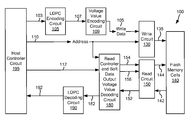
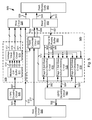
- Solid state storage system 100 includes soft data output voltage value decoding circuitry in accordance with some embodiments of the present invention.
- Solid state storage system 100 includes a host controller circuit 195 , a low density parity check encoding circuit 105 , a voltage value encoding circuit 109 , a write circuit 130 , flash memory cells 140 , a read circuit 150 , a read controller and soft data output voltage value decoding circuit 180 , and a low density parity check decoding circuit 190 .
- Host controller circuit 195 directs read and write access to flash memory cells 140 .
- Flash memory cells 140 may be NAND flash memory cells or another type of solid state memory cells as are known in the art.
- a data write is effectuated when host controller circuit 195 provides input data 103 to low density parity check encoding circuit 105 .
- Low density parity check encoding circuit 105 applies a low density parity check encoding algorithm to input data 103 to yield LDPC codewords 107 .
- LDPC codewords 107 are provided to voltage value encoding circuit 109 .
- Voltage value encoding circuit 109 applies multi-level cell encoding to a group of LDPC codewords 107 to yield write data 111 .
- five LDPC codewords are encoded together to yield write data 111 that is directed to flash memory cells 140 that are written as two-bit cells. It should be noted that while the various embodiments are discussed in relation to using a low density parity check encoding/decoding algorithm, that other encoding/decoding algorithms known in the art may be used in accordance with other embodiments of the present invention.
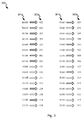
- FIG. 2 an example of multi-level cell encoding 200 using multiple low density parity check codewords 201 , 203 , 205 , 207 , 209 to yield a series of five bit words that are encoded into write data in accordance with some embodiments of the present invention.
- Each of the low density parity check codewords 201 , 203 , 205 , 207 , 209 includes a number of bits indicated as positions (i.e., position 1, position 2, . . . position n ⁇ 1, and position n). It should be noted that an element (e.g., bit) of each of the respective codewords is found at each position.
- a five bit word includes the first element of each of the five low density parity check codewords 201 , 203 , 205 , 207 , 209 (i.e., ⁇ A 1 , B 1 , C 1 , D 1 , E 1 ⁇ ). This is repeated for each of the positions 1 through n to yield n five bit words (i.e., ⁇ A 2 , B 2 , C 2 , D 2 , E 2 ⁇ . . . ⁇ A n , B n , C n , D n , E n ⁇ ).
- voltage value encoding circuit 109 encodes each of the n five bit words discussed in relation to FIG. 2 to a corresponding three value output that is provided as write data 111 .
- a five bit word 301 a , 301 b ( ⁇ A, B, C, D, E ⁇ ) to three voltage levels 303 a , 303 b ( ⁇ X, Y, Z ⁇ ) conversion table 300 is shown in accordance with some embodiments of the present invention.
- five bit word 301 a , 301 b correspond to the five bit words ( ⁇ A, B, C, D, E ⁇ ) discussed above in relation to FIG. 2 .
- FIG. 4 a another five bit word 401 a , 401 b ( ⁇ A, B, C, D, E ⁇ ) to three voltage levels 403 a , 403 b ( ⁇ X, Y, Z ⁇ ) conversion table 400 in accordance with some embodiments of the present invention.
- five bit word 401 a , 401 b correspond to the five bit words ( ⁇ A, B, C, D, E ⁇ ) discussed above in relation to FIG. 2 .
- the corresponding three voltage levels are “2, 2, 0”.
- three voltage levels are “3, 1, 2”
- the corresponding five bit word is ‘10101’.
- the aforementioned conversion tables are from five bit words to three voltage levels, other conversions may be possible in accordance with various embodiments of the present invention.
- other embodiments of the present invention may use conversion tables from four bit words to three voltage levels. Based upon the disclosure provided herein, one of ordinary skill in the art will recognize other conversion tables that may be used in accordance with various embodiments of the present invention.
- write data 111 is provided to a write circuit 130 .
- write circuit 130 receives an address 110 is received from host controller circuit 195 .
- Write circuit 130 converts the voltage levels (e.g., ⁇ X, Y, Z ⁇ ) received as write data 111 into a series of voltages 135 that are written to three cells of flash memory cells 140 indicated by address 110 .
- a voltage level of “0” results in voltage 135 being set below a lower threshold (V L )
- a voltage level of “1” results in voltage 135 being set above the lower threshold (V L ) and below a center threshold (V C )
- a voltage level of “2” results in voltage 135 being set above the center threshold (V C ) and below an upper threshold (V U )
- a voltage level of “3” results in voltage 135 being set above the upper threshold (V U ).
- This process results in storing three voltage values respectively to three cells within flash memory cells to represent a five bit word. This process is repeated for each of the five bit words resulting in a group of multiple sets of three flash memory cells representing the five LDPC codewords received as LDPC codewords 107 .
- a data read is effectuated when host controller circuit 195 provides a read request indication 112 and address 110 to read controller and soft data output voltage value decoding circuit 180 .
- Read controller and soft data output voltage value decoding circuit 180 translates read request 112 and address 110 into an address 154 and a threshold value 156 (or series of threshold values) that are provided to a read circuit 150 .
- a read location 144 is generated based upon address 154 and provided to flash memory cells 140 .
- flash memory cells 140 provides return voltages 142 stored at the cells indicated by read location 144 .
- Read circuit 150 compares return voltages 142 with threshold 156 to yield corresponding binary values 152 .
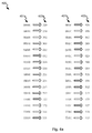
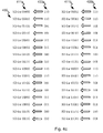
- FIG. 4 b a first part of the aforementioned process of comparing return voltages 142 with threshold 156 is shown where the conversion of FIG. 4 a was used in the original encoding.
- This first part recovers a soft data representation of the first LDPC codeword (i.e., low density parity check codeword 201 ).
- a table 410 represents conversion of the three voltage levels 403 a , 403 b ( ⁇ X, Y, Z ⁇ ) of FIG. 4 a where threshold 156 is the lower threshold (V L ).
- any voltage value received as return voltages 142 that is less than V L results in a binary ‘0’
- any voltage value received as return voltages 142 that is greater than or equal to V L results in a binary ‘1’
- the corresponding binary output i.e., binary values 152
- the corresponding binary output is ‘110’ (shown as values 413 a , 413 b ).
- the corresponding binary output is ‘111’ (shown as values 413 a , 413 b ).
- These binary values map to a single soft data value corresponding to one LDPC codeword (i.e., low density parity check codeword 201 ).
- the three bit binary values 413 a , 413 b map to soft data for a corresponding five bit word (i.e., SD for XXXX 411 a , 411 b ).
- the conversion process may be done using a look up table that is loaded with pre-calculated soft data values corresponding to the respective three bit binary values.
- the soft data values corresponding to the respective three bit binary values may be calculated on the fly based upon the respective three bit binary values. Comparison of the next set of three cells of flash memory cells with V L is performed to yield the soft data value corresponding to the next bit of the LDPC codeword (i.e., low density parity check codeword 201 ). This process is repeated until soft data values corresponding to all bits of the LDPC codeword are generated (i.e., low density parity check codeword 201 ).
- the soft data values for any bit of a five bit word corresponding to the respective three bit binary values are calculated (either pre-calculated and stored to a look-up table, or calculated on the fly using a calculation circuit) in accordance with the following equation:
- LLR is a log-likelihood ratio
- Y represents the three bit value 413 a , 413 b derived from flash memory cells 140
- p represents the position in the five bit word
- b p represents the binary value for the bit at position p.
- C are the three voltages provided from flash memory cells;
- Probability ⁇ ⁇ ( C , Y ) Probability ⁇ ⁇ ( Y
- C ′ ) , where Probability ⁇ ⁇ ( Y , C ) Probability ⁇ ⁇ ( Y
- quantized inputs are used in place of the three bit binary values.
- the soft data output corresponding to the quantized inputs is calculated in accordance with the following equation:
- U represents a quantized version of the three bit value 413 a , 413 b derived from flash memory cells 140 .
- FIG. 4 c a second part of the aforementioned process of comparing return voltages 142 with threshold 156 is shown where the conversion of FIG. 4 a was used in the original encoding.
- This second part recovers the second and third LDPC codewords (i.e., low density parity check codeword 203 and low density parity check codeword 205 ).
- a table 430 represents conversion of the three voltage levels 403 a , 403 b ( ⁇ X, Y, Z ⁇ ) of FIG. 4 a where threshold 156 is the center threshold (V C ).
- any voltage value received as return voltages 142 that is less than V C results in a binary ‘0’
- any voltage value received as return voltages 142 that is greater than or equal to V C results in a binary ‘1’
- the corresponding binary output i.e., binary values 152
- the corresponding binary output is ‘110’ (shown as values 433 a , 433 b ).
- the corresponding binary output is ‘101’ (shown as values 433 a , 433 b ).
- These binary values map to two soft data values corresponding to two LDPC codewords (i.e., low density parity check codeword 203 and low density parity check codeword 205 ).
- the three bit binary values 433 a , 433 b map to soft data for a corresponding five bit word (i.e., SD for XXXX 411 a , 411 b ).
- the conversion process may be done using a look up table that is loaded with pre-calculated soft data values corresponding to the respective three bit binary values.
- the soft data values corresponding to the respective three bit binary values may be calculated on the fly based upon the respective three bit binary values.
- the conversion may be done in accordance with the equations discussed above in relation to FIG. 4 b .
- Comparison of the next set of three cells of flash memory cells with V C is performed to yield the soft data values corresponding to the next bits of the two LDPC codewords (i.e., low density parity check codeword 203 and low density parity check codeword 205 ). This process is repeated until soft data values corresponding to all bits of the LDPC codewords are generated (i.e., low density parity check codeword 203 and low density parity check codeword 205 ).
- a ‘111’ pattern is an invalid value, but a soft data value is generated for it and all other valid patterns.
- FIG. 4 d a third part of the aforementioned process of comparing return voltages 142 with threshold 156 is shown where the conversion of FIG. 4 a was used in the original encoding.
- This third part recovers the fourth and fifth LDPC codewords (i.e., low density parity check codeword 207 and low density parity check codeword 209 ).
- a table 450 represents conversion of the three voltage levels 403 a , 403 b ( ⁇ X, Y, Z ⁇ ) of FIG. 4 a where threshold 156 is the upper threshold (V U ).
- any voltage value received as return voltages 142 that is less than V U results in a binary ‘0’
- any voltage value received as return voltages 142 that is greater than or equal to V U results in a binary ‘1’
- the corresponding binary output i.e., binary values 152
- the corresponding binary output is ‘000’ (shown as values 453 a , 453 b ).
- the corresponding binary output is ‘100’ (shown as values 453 a , 453 b ).
- These binary values map to two soft data values corresponding to two LDPC codewords (i.e., low density parity check codeword 203 and low density parity check codeword 205 ).
- the three bit binary values 453 a , 453 b map to soft data for a corresponding five bit word (i.e., SD for XXXX 411 a , 411 b ).
- the conversion process may be done using a look up table that is loaded with pre-calculated soft data values corresponding to the respective three bit binary values.
- the soft data values corresponding to the respective three bit binary values may be calculated on the fly based upon the respective three bit binary values.
- the conversion may be done in accordance with the equations discussed above in relation to FIG. 4 b .
- Comparison of the next set of three cells of flash memory cells with V U is performed to yield the soft data values corresponding to the next bits of the two LDPC codewords (i.e., low density parity check codeword 207 and low density parity check codeword 209 ). This process is repeated until soft data values corresponding to all bits of the LDPC codewords are generated (i.e., low density parity check codeword 207 and low density parity check codeword 209 ).
- a ‘111’ pattern is an invalid value, but a soft data value is generated for it and all other valid patterns.
- Binary values 152 are provided to read controller and soft data output voltage value decoding circuit 180 where they are decoded to yield soft data 182 corresponding to the underlying LDPC codewords (i.e., soft data representation of the originally encoded LDPC codewords 107 ).
- Soft data 182 corresponding to the underlying LDPC codewords is provided low density parity check decoding circuit 190 .
- Low density parity check decoding circuit 190 applies a low density parity check decoding algorithm to soft data 182 to yield recovered read data 192 that is provided to host controller circuit 195 .
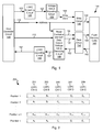
- Solid state storage system 500 includes soft data output voltage value decoding circuitry in accordance with some embodiments of the present invention.
- Solid state storage system 500 includes a host controller circuit 595 , a low density parity check encoding circuit 505 , a voltage value encoding circuit 509 shown in dashed lines, a write circuit 530 , flash memory cells 540 , a read circuit 550 , a read controller and soft data output voltage value decoding circuit 580 shown in dashed lines, and a low density parity check decoding circuit 590 .
- Read controller and soft data output voltage value decoding circuit 580 includes a read controller circuit 570 , a serial to parallel buffer circuit 560 , and three page soft data output decoding circuits 574 , 576 , 578 .
- Voltage value encoding circuit 509 includes a multiple codeword buffer circuit 511 and a multi-level cell encoder circuit 515 .
- Host controller circuit 595 directs read and write access to flash memory cells 540 . Flash memory cells 540 may be NAND flash memory cells or another type of solid state memory cells as are known in the art.
- a data write is effectuated when host controller circuit 595 provides input data 503 to low density parity check encoding circuit 505 .
- Low density parity check encoding circuit 505 applies a low density parity check encoding algorithm to input data 503 to yield LDPC codewords 507 .
- Low density parity check encoding circuit 505 may be any circuit known in the art that is capable of receiving user data and generating corresponding low density parity check codewords.
- LDPC codewords 507 are provided to multi-level cell encoding circuit 509 .
- Multiple codeword buffer circuit 511 of voltage value encoding circuit 509 stores five LDPC codewords received as LDPC codewords 507 .
- Voltage value 517 corresponds to a voltage level that is to be written to a first of a three cell block of flash memory cells 540
- voltage value 519 corresponds to a voltage level that is to be written to a second of the three cell block of flash memory cells 140
- voltage value 521 corresponds to a voltage level that is to be written to a third of the three cell block of flash memory cells 540
- voltage values 517 , 519 , 521 may be one of four voltage levels each representing a two-bit pattern stored in a given cell of flash memory cells 540 . It should be noted that in other embodiments, eight or more voltage levels representing three or more bits stored in a given cell of flash memory cells 540 are possible in accordance with other embodiments of the present invention.
- multi-level cell encoding 200 is shown using multiple low density parity check codewords 201 , 203 , 205 , 207 , 209 to yield a series of five bit words 513 that are encoded into write data in accordance with some embodiments of the present invention.
- Each of the low density parity check codewords 201 , 203 , 205 , 207 , 209 includes a number of bits indicated as positions (i.e., position 1, position 2, . . . position n ⁇ 1, and position n).
- a five bit word 513 includes the first element of each of the five low density parity check codewords 201 , 203 , 205 , 207 , 209 (i.e., ⁇ A 1 , B 1 , C 1 , D 1 , E 1 ⁇ ). This is repeated for each of the positions 1 through n to yield n five bit words 513 (i.e., ⁇ A 2 , B 2 , C 2 , D 2 , E 2 ⁇ . . . ⁇ A n , B n , C n , D n , E n ⁇ ).
- multi-level cell encoder circuit 515 encodes each of the n five bit words 513 to a corresponding three value output that is provided as voltage values 517 , 519 , 521 to write circuit 530 .
- a five bit word 301 a , 301 b ( ⁇ A, B, C, D, E ⁇ ) to three voltage levels 303 a , 303 b ( ⁇ X, Y, Z ⁇ ) conversion table 300 is shown in accordance with some embodiments of the present invention.
- five bit word 301 a , 301 b correspond to the five bit words ( ⁇ A, B, C, D, E ⁇ ) discussed above in relation to FIG. 2 .
- FIG. 4 a another five bit word 401 a , 401 b ( ⁇ A, B, C, D, E ⁇ ) to three voltage levels 403 a , 403 b ( ⁇ X, Y, Z ⁇ ) conversion table 400 in accordance with some embodiments of the present invention.
- five bit word 401 a , 401 b correspond to the five bit words ( ⁇ A, B, C, D, E ⁇ ) discussed above in relation to FIG. 2 .
- the corresponding three voltage levels are “2, 2, 0”.
- three voltage levels are “3, 1, 2”
- the corresponding five bit word is ‘10101’.
- the aforementioned conversion tables are from five bit words to three voltage levels, other conversions may be possible in accordance with various embodiments of the present invention.
- other embodiments of the present invention may use conversion tables from four bit words to three voltage levels. Based upon the disclosure provided herein, one of ordinary skill in the art will recognize other conversion tables that may be used in accordance with various embodiments of the present invention.
- write circuit 530 additionally receives an address 510 from host controller circuit 595 .
- Write circuit 530 converts voltage values 517 , 519 , 521 (e.g., ⁇ X, Y, Z ⁇ ) into a series of voltages 535 that are written to three cells of flash memory cells 540 indicated by address 510 .
- a voltage level of “0” results in voltage 535 being set below a lower threshold (V L )
- a voltage level of “1” results in voltage 535 being set above the lower threshold (V L ) and below a center threshold (V C )
- a voltage level of “2” results in voltage 535 being set above the center threshold (V C ) and below an upper threshold (V U )
- a voltage level of “3” results in voltage 535 being set above the upper threshold (V U ).
- This process results in storing three voltage values respectively to three cells within flash memory cells to represent a five bit word. This process is repeated for each of the five bit words resulting in a group of multiple sets of three flash memory cells representing the five LDPC codewords received as LDPC codewords 507 .
- a data read is effectuated when host controller circuit 595 provides a read request indication 512 and address 510 to read controller circuit 570 of read controller and soft data output voltage value decoding circuit 580 .
- Read controller circuit 570 translates read request 512 and address 510 into an address 554 and a threshold value 556 (or series of threshold values) that are provided to read circuit 550 .
- a read location 544 is generated by read circuit 550 based upon address 554 and provided to flash memory cells 540 .
- flash memory cells 540 provides return voltages 542 stored at the cells indicated by read location 544 .
- Read circuit 550 compares return voltages 542 with threshold 556 to yield corresponding binary values 552 .
- Binary values 552 are provided to serial to parallel buffer 560 that assembles the binary values into sets of three bits 562 , 564 , 566 associated with the same five bit words. Bits 562 , 564 , 566 are provided to each of page 0 soft data output decoding circuit 574 , page 1 soft data output decoding circuit 576 , and page 2 soft data output decoding circuit 578 . Based upon the ongoing read, read controller circuit 570 asserts various enables 572 that enable operation of respective ones of page 0 soft data output decoding circuit 574 , page 1 soft data output decoding circuit 576 , and page 2 soft data output decoding circuit 578 .
- read controller circuit 570 sequentially provides: the lower threshold (V L ) to obtain the soft data corresponding to the first LDPC codeword represented in the five bit words, the center threshold (V C ) to obtain the soft data corresponding to the second and third LDPC codewords represented in the five bit words, and the upper threshold (V U ) to obtain the soft data corresponding to the fourth and fifth LDPC codewords represented in the five bit words as threshold value 556 .
- some subset of the lower threshold (V L ), the center threshold (V C ), and/or the upper threshold (V U ) are sequentially presented as threshold value 556 .
- the center threshold (V C ), and/or the upper threshold (V U ) are sequentially presented as threshold value 556 .
- the upper threshold (V U ) is presented.
- V L threshold
- enables 572 are asserted by read controller circuit 570 such that operation of page 0 soft data output decoding circuit 574 is enabled, while operation of page 1 soft data output decoding circuit 576 and page 2 soft data output decoding circuit 578 is disabled.
- page 0 soft data output decoding circuit 574 When enabled, page 0 soft data output decoding circuit 574 generates soft data corresponding to the first LDPC codeword represented in the five bit words based upon bits 562 , 564 , 566 corresponding to the result of comparing return voltages 542 with the lower threshold (V L ). The generated soft data corresponding to the first LDPC codeword is provided as a soft data output 582 to LDPC decoding circuit 590 .
- page 1 soft data output decoding circuit 576 when enabled, page 1 soft data output decoding circuit 576 generates soft data corresponding to the second and third LDPC codewords represented in the five bit words based upon bits 562 , 564 , 566 corresponding to the result of comparing return voltages 542 with the center threshold (V C ).
- the generated soft data corresponding to the second and third LDPC codewords is provided as a soft data output 584 to LDPC decoding circuit 590 .
- page 2 soft data output decoding circuit 578 when enabled, page 2 soft data output decoding circuit 578 generates soft data corresponding to the fourth and fifth LDPC codewords represented in the five bit words based upon bits 562 , 564 , 566 corresponding to the result of comparing return voltages 542 with the upper threshold (V U ).
- the generated soft data corresponding to the fourth and fifth LDPC codewords is provided as a soft data output 586 to LDPC decoding circuit 590 .
- FIG. 4 b a first part of the aforementioned process of comparing return voltages 542 with threshold 556 is shown where the conversion of FIG. 4 a was used in the original encoding.
- This first part recovers a soft data representation of the first LDPC codeword (i.e., low density parity check codeword 201 ).
- a table 410 represents conversion of the three voltage levels 403 a , 403 b ( ⁇ X, Y, Z ⁇ ) of FIG. 4 a where threshold 556 is the lower threshold (V L ).
- any voltage value received as return voltages 542 that is less than V L results in a binary ‘0’
- any voltage value received as return voltages 542 that is greater than or equal to V L results in a binary ‘1’
- the corresponding binary output i.e., binary values 552
- the corresponding binary output is ‘110’ (shown as values 413 a , 413 b ).
- the corresponding binary output is ‘111’ (shown as values 413 a , 413 b ).
- These binary values map to a single soft data value corresponding to one LDPC codeword (i.e., low density parity check codeword 201 ).
- the three bit binary values 413 a , 413 b map to soft data for a corresponding five bit word (i.e., SD for XXXX 411 a , 411 b ).
- the conversion process may be done using a look up table that is loaded with pre-calculated soft data values corresponding to the respective three bit binary values.
- the soft data values corresponding to the respective three bit binary values may be calculated on the fly based upon the respective three bit binary values. Comparison of the next set of three cells of flash memory cells with V L is performed to yield the soft data value corresponding to the next bit of the LDPC codeword (i.e., low density parity check codeword 201 ). This process is repeated until soft data values corresponding to all bits of the LDPC codeword are generated (i.e., low density parity check codeword 201 ).
- the soft data values for any bit of a five bit word corresponding to the respective three bit binary values are calculated (either pre-calculated and stored to a look-up table, or calculated on the fly using a calculation circuit) in accordance with the following equation:
- LLR is a log-likelihood ratio
- Y represents the three bit value 413 a , 413 b derived from flash memory cells 540
- p represents the position in the five bit word
- b p represents the binary value for the bit at position p.
- C are the three voltages provided from flash memory cells;
- Probability ⁇ ⁇ ( C , Y ) Probability ⁇ ⁇ ( Y
- C ′ ) , where Probability ⁇ ⁇ ( Y , C ) Probability ⁇ ⁇ ( Y
- quantized inputs are used in place of the three bit binary values.
- the soft data output corresponding to the quantized inputs is calculated in accordance with the following equation:
- U represents a quantized version of the three bit value 413 a , 413 b derived from flash memory cells 540 .
- FIG. 4 c a second part of the aforementioned process of comparing return voltages 542 with threshold 556 is shown where the conversion of FIG. 4 a was used in the original encoding.
- This second part recovers the second and third LDPC codewords (i.e., low density parity check codeword 203 and low density parity check codeword 205 ).
- a table 430 represents conversion of the three voltage levels 403 a , 403 b ( ⁇ X, Y, Z ⁇ ) of FIG. 4 a where threshold 556 is the center threshold (V C ).
- any voltage value received as return voltages 542 that is less than V C results in a binary ‘0’
- any voltage value received as return voltages 542 that is greater than or equal to V C results in a binary ‘1’
- the corresponding binary output i.e., binary values 552
- the corresponding binary output is ‘110’ (shown as values 433 a , 433 b ).
- the corresponding binary output is ‘101’ (shown as values 433 a , 433 b ).
- These binary values map to two soft data values corresponding to two LDPC codewords (i.e., low density parity check codeword 203 and low density parity check codeword 205 ).
- the three bit binary values 433 a , 433 b map to soft data for a corresponding five bit word (i.e., SD for XXXX 411 a , 411 b ).
- the conversion process may be done using a look up table that is loaded with pre-calculated soft data values corresponding to the respective three bit binary values.
- the soft data values corresponding to the respective three bit binary values may be calculated on the fly based upon the respective three bit binary values.
- the conversion may be done in accordance with the equations discussed above in relation to FIG. 4 b .
- Comparison of the next set of three cells of flash memory cells with V C is performed to yield the soft data values corresponding to the next bits of the two LDPC codewords (i.e., low density parity check codeword 203 and low density parity check codeword 205 ). This process is repeated until soft data values corresponding to all bits of the LDPC codewords are generated (i.e., low density parity check codeword 203 and low density parity check codeword 205 ).
- a ‘111’ pattern is an invalid value, but a soft data value is generated for it and all other valid patterns.
- FIG. 4 d a second part of the aforementioned process of comparing return voltages 542 with threshold 556 is shown where the conversion of FIG. 4 a was used in the original encoding.
- This second part recovers the fourth and fifth LDPC codewords (i.e., low density parity check codeword 207 and low density parity check codeword 209 ).
- a table 450 represents conversion of the three voltage levels 403 a , 403 b ( ⁇ X, Y, Z ⁇ ) of FIG. 4 a where threshold 556 is the upper threshold (V U ).
- any voltage value received as return voltages 542 that is less than V U results in a binary ‘0’
- any voltage value received as return voltages 542 that is greater than or equal to V U results in a binary ‘1’
- the corresponding binary output i.e., binary values 552
- the corresponding binary output is ‘000’ (shown as values 453 a , 453 b ).
- the corresponding binary output is ‘100’ (shown as values 453 a , 453 b ).
- These binary values map to two soft data values corresponding to two LDPC codewords (i.e., low density parity check codeword 203 and low density parity check codeword 205 ).
- the three bit binary values 453 a , 453 b map to soft data for a corresponding five bit word (i.e., SD for XXXX 411 a , 411 b ).
- the conversion process may be done using a look up table that is loaded with pre-calculated soft data values corresponding to the respective three bit binary values.
- the soft data values corresponding to the respective three bit binary values may be calculated on the fly based upon the respective three bit binary values.
- the conversion may be done in accordance with the equations discussed above in relation to FIG. 4 b .
- Comparison of the next set of three cells of flash memory cells with V C is performed to yield the soft data values corresponding to the next bits of the two LDPC codewords (i.e., low density parity check codeword 207 and low density parity check codeword 209 ). This process is repeated until soft data values corresponding to all bits of the LDPC codewords are generated (i.e., low density parity check codeword 207 and low density parity check codeword 209 ).
- a ‘111’ pattern is an invalid value, but a soft data value is generated for it and all other valid patterns.
- Low density parity check decoding circuit 590 applies a low density parity check decoding algorithm to the resulting soft data values corresponding to LDPC codewords provided as soft data output 582 , soft data output 584 and/or soft data output 586 to yield recovered read data 592 that is provided to host controller circuit 595 .
- page 0 soft data output decoding circuit 574 , page 1 soft data output decoding circuit 576 , and page 2 soft data output decoding circuit 578 are implemented as look-up tables, three look-up tables are used—one for each of page 0 , page 1 and page 2 .
- Each of the aforementioned look-up tables includes 2 N entries where N is three in the case of three bit binary values.
- each of the aforementioned look-up tables includes NU N entries where NU is the number of bins which for the aforementioned embodiments is two.
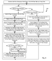
- a flow diagram 600 shows a method in accordance with various embodiments of the present invention for efficient storage and access to/from flash memory cells. Following flow diagram 600 , it is determined whether a read request is received (block 605 ). Where a read request has not been received (block 605 ), it is determined whether a write request is received (block 695 ). Where a write request has been received (block 695 ), low density parity encoding is applied to a user data set received as part of the write request (block 607 ).
- the aforementioned process includes grouping corresponding elements of the five LDPC codewords to yield groups of five bit words.
- FIG. 2 an example of multi-level cell encoding 200 using multiple low density parity check codewords 201 , 203 , 205 , 207 , 209 to yield a series of five bit words that are encoded into write data in accordance with some embodiments of the present invention.
- Each of the low density parity check codewords 201 , 203 , 205 , 207 , 209 includes a number of bits indicated as positions (i.e., position 1, position 2, . . . position n ⁇ 1, and position n).
- a five bit word includes the first element of each of the five low density parity check codewords 201 , 203 , 205 , 207 , 209 (i.e., ⁇ A 1 , B 1 , C 1 , D 1 , E 1 ⁇ ). This is repeated for each of the positions 1 through n to yield n five bit words (i.e., ⁇ A 2 , B 2 , C 2 , D 2 , E 2 ⁇ . . . ⁇ A n , B n , C n , D n , E n ⁇ ).
- a five bit word 301 a , 301 b ( ⁇ A, B, C, D, E ⁇ ) to/from three voltage levels 303 a , 303 b ( ⁇ X, Y, Z ⁇ ) conversion table 300 is shown in accordance with some embodiments of the present invention.
- five bit word 301 a , 301 b correspond to the five bit words ( ⁇ A, B, C, D, E ⁇ ) discussed above in relation to FIG. 2 .
- FIG. 4 a another five bit word 401 a , 401 b ( ⁇ A, B, C, D, E ⁇ ) to/from three voltage levels 403 a , 403 b ( ⁇ X, Y, Z ⁇ ) conversion table 400 in accordance with some embodiments of the present invention.
- five bit word 401 a , 401 b correspond to the five bit words ( ⁇ A, B, C, D, E ⁇ ) discussed above in relation to FIG. 2 .
- the corresponding three voltage levels are “2, 2, 0”.
- three voltage levels are “3, 1, 2”
- the corresponding five bit word is ‘10101’.
- the aforementioned conversion tables are from five bit words to three voltage levels, other conversions may be possible in accordance with various embodiments of the present invention.
- other embodiments of the present invention may use conversion tables from four bit words to three voltage levels. Based upon the disclosure provided herein, one of ordinary skill in the art will recognize other conversion tables that may be used in accordance with various embodiments of the present invention.
- each of the three voltage levels for each of the groups of three voltage levels are converted to corresponding voltage values (block 627 ).
- a voltage level of “0” i.e., for a value of X, Y or Z equal to zero
- a voltage level of “1” i.e., for a value of X, Y or Z equal to one
- a voltage level of “2” i.e., for a value of X, Y or Z equal to two
- a voltage level of “3” i.e., for a value of X, Y or Z equal to three
- These voltage values are then written to three cells of a flash memory device (block 637 ). This process results in storing three voltage values respectively to three cells within flash memory cells to represent a five bit word. This process is repeated for each of the five bit words resulting in a group of multiple sets of three flash memory cells representing the five LDPC codewords encoded from the originally received user data.
- pages corresponding to the request are identified (block 610 ). For example, if only the first of the LDPC codewords encoded to yield the set of groups of three voltage levels in block 617 is to be read, then only page 0 is identified. Alternatively, if only or both of the second and third of the LDPC codewords encoded to yield the set of groups of three voltage levels in block 617 is to be read, then only page 1 is identified. As yet another alternative, if only or both of the fourth and fifth of the LDPC codewords encoded to yield the set of groups of three voltage levels in block 617 is to be read, then only page 2 is identified.
- the first of the identified pages is selected (block 615 ). Thus, for example, if only one page is to be read, then that one page is selected. If more than one page is to be read, then one of the more than one pages is selected. A threshold corresponding to the selected page to be read is selected (block 620 ). Thus, for example, if page 0 is selected to be read then lower threshold (V L ) is selected. Alternatively, if page 1 is selected to be read then center threshold (V C ) is selected. Alternatively, if page 2 is selected to be read then upper threshold (V U ) is selected.
- the flash memory cells corresponding to the read request are read using the selected threshold to yield a binary data set corresponding to the selected page (block 625 ).
- the binary data set includes the first LDPC codeword (i.e., low density parity check codeword 201 ).
- the binary data set includes the second and third LDPC codewords (i.e., low density parity check codeword 203 and low density parity check codeword 205 ).
- the binary data set includes the fourth and fifth LDPC codewords (i.e., low density parity check codeword 207 and low density parity check codeword 209 ). This read yields a series of groups of three binary values for each group of three flash memory cells that are read.
- Soft data corresponding to the selected page is accessed to yield the soft data output corresponding to the three bit data in the binary data set where the soft data indicates a likelihood that bits in a particular position in the five bit word are correct (block 630 ).
- FIG. 4 b a first part of the aforementioned process of comparing return voltages with the selected threshold is shown where the conversion of FIG. 4 a was used in the original encoding. This first part recovers a soft data representation of the first LDPC codeword (i.e., low density parity check codeword 201 ).
- a table 410 represents conversion of the three voltage levels 403 a , 403 b ( ⁇ X, Y, Z ⁇ ) of FIG.
- the selected threshold is the lower threshold (V L ).
- V L the lower threshold
- any voltage value received as return voltages that is less than V L results in a binary ‘0’
- any voltage value received as return voltages that is greater than or equal to V L results in a binary ‘1’
- the corresponding binary output is ‘110’ (shown as values 413 a , 413 b ).
- the corresponding binary output is ‘111’ (shown as values 413 a , 413 b ).
- These binary values map to a single soft data value corresponding to one LDPC codeword (i.e., low density parity check codeword 201 ).
- the three bit binary values 413 a , 413 b map to soft data for a corresponding five bit word (i.e., SD for XXXX 411 a , 411 b ).
- the conversion process may be done using a look up table that is loaded with pre-calculated soft data values corresponding to the respective three bit binary values.
- the soft data values corresponding to the respective three bit binary values may be calculated on the fly based upon the respective three bit binary values. Comparison of the next set of three cells of flash memory cells with V L is performed to yield the soft data value corresponding to the next bit of the LDPC codeword (i.e., low density parity check codeword 201 ). This process is repeated until soft data values corresponding to all bits of the LDPC codeword are generated (i.e., low density parity check codeword 201 ).
- the soft data values for any bit of a five bit word corresponding to the respective three bit binary values are calculated (either pre-calculated and stored to a look-up table, or calculated on the fly using a calculation circuit) in accordance with the following equation:
- LLR is a log-likelihood ratio
- Y represents the three bit value 413 a , 413 b derived from flash memory cells 540
- p represents the position in the five bit word
- b p represents the binary value for the bit at position p.
- C are the three voltages provided from flash memory cells;
- Probability ⁇ ⁇ ( C , Y ) Probability ⁇ ⁇ ( Y
- C ′ ) , where Probability ⁇ ⁇ ( Y , C ) Probability ⁇ ⁇ ( Y
- quantized inputs are used in place of the three bit binary values.
- the soft data output corresponding to the quantized inputs is calculated in accordance with the following equation:
- FIG. 4 c a second part of the aforementioned process of comparing the return voltages with the selected threshold is shown where the conversion of FIG. 4 a was used in the original encoding.
- This second part recovers the second and third LDPC codewords (i.e., low density parity check codeword 203 and low density parity check codeword 205 ).
- a table 430 represents conversion of the three voltage levels 403 a , 403 b ( ⁇ X, Y, Z ⁇ ) of FIG. 4 a where the selected threshold is the center threshold (V C ).
- any voltage value received as the return voltages that is less than V C results in a binary ‘0’
- any voltage value received as the return voltages that is greater than or equal to V C results in a binary ‘1’
- the corresponding binary output is ‘110’ (shown as values 433 a , 433 b ).
- the corresponding binary output is ‘101’ (shown as values 433 a , 433 b ).
- These binary values map to two soft data values corresponding to two LDPC codewords (i.e., low density parity check codeword 203 and low density parity check codeword 205 ).
- the three bit binary values 433 a , 433 b map to soft data for a corresponding five bit word (i.e., SD for XXXX 411 a , 411 b ).
- the conversion process may be done using a look up table that is loaded with pre-calculated soft data values corresponding to the respective three bit binary values.
- the soft data values corresponding to the respective three bit binary values may be calculated on the fly based upon the respective three bit binary values.
- the conversion may be done in accordance with the equations discussed above in relation to FIG. 4 b .
- Comparison of the next set of three cells of flash memory cells with V C is performed to yield the soft data values corresponding to the next bits of the two LDPC codewords (i.e., low density parity check codeword 203 and low density parity check codeword 205 ). This process is repeated until soft data values corresponding to all bits of the LDPC codewords are generated (i.e., low density parity check codeword 203 and low density parity check codeword 205 ).
- a ‘111’ pattern is an invalid value, but a soft data value is generated for it and all other valid patterns.
- FIG. 4 d a third part of the aforementioned process of comparing the return voltages with the selected threshold is shown where the conversion of FIG. 4 a was used in the original encoding.
- This third part recovers the second and third LDPC codewords (i.e., low density parity check codeword 207 and low density parity check codeword 209 ).
- a table 450 represents conversion of the three voltage levels 403 a , 403 b ( ⁇ X, Y, Z ⁇ ) of FIG. 4 a where the selected threshold is the upper threshold (V U ).
- any voltage value received as the return voltages that is less than V U results in a binary ‘0’
- any voltage value received as the return voltages that is greater than or equal to V U results in a binary ‘1’
- the corresponding binary output is ‘000’ (shown as values 453 a , 453 b ).
- the corresponding binary output is ‘100’ (shown as values 453 a , 453 b ).
- These binary values map to two soft data values corresponding to two LDPC codewords (i.e., low density parity check codeword 203 and low density parity check codeword 205 ).
- the three bit binary values 453 a , 453 b map to soft data for a corresponding five bit word (i.e., SD for XXXX 411 a , 411 b ).
- the conversion process may be done using a look up table that is loaded with pre-calculated soft data values corresponding to the respective three bit binary values.
- the soft data values corresponding to the respective three bit binary values may be calculated on the fly based upon the respective three bit binary values.
- the conversion may be done in accordance with the equations discussed above in relation to FIG. 4 b .
- Comparison of the next set of three cells of flash memory cells with V U is performed to yield the soft data values corresponding to the next bits of the two LDPC codewords (i.e., low density parity check codeword 207 and low density parity check codeword 209 ). This process is repeated until soft data values corresponding to all bits of the LDPC codewords are generated (i.e., low density parity check codeword 207 and low density parity check codeword 209 ).
- a ‘111’ pattern is an invalid value, but a soft data value is generated for it and all other valid patterns.
- Such integrated circuits may include all of the functions of a given block, system or circuit, or a subset of the block, system or circuit. Further, elements of the blocks, systems or circuits may be implemented across multiple integrated circuits. Such integrated circuits may be any type of integrated circuit known in the art including, but are not limited to, a monolithic integrated circuit, a flip chip integrated circuit, a multichip module integrated circuit, and/or a mixed signal integrated circuit. It should also be noted that various functions of the blocks, systems or circuits discussed herein may be implemented in either software or firmware.
- the entire system, block or circuit may be implemented using its software or firmware equivalent—albeit such a system entirely implemented in software or firmware would not be a circuit.
- the one part of a given system, block or circuit may be implemented in software or firmware, while other parts are implemented in hardware.
Abstract
Description
- Embodiments are related to systems and methods for data storage, and more particularly to systems and methods for storing to and accessing data from a flash memory.
- To increase density in a flash memory device, multi-level cells are used. Such multi-level cells may be, for example, programmed to with one of four voltage levels with each of the four voltage levels representing a two bit binary value. When reading such a multi-level cell, a read back voltage is compared with a center voltage threshold to determine the least significant bit of the two bit binary value and additional comparisons are performed with an upper voltage threshold and a lower voltage threshold to determine the most significant bit of the two bit binary value. Use of multiple comparisons to yield the two bit binary value results in considerable latency.
- Hence, for at least the aforementioned reasons, there exists a need in the art for advanced systems and methods for storing to and accessing data from a flash memory.
- Embodiments are related to systems and methods for data storage, and more particularly to systems and methods for storing to and accessing data from a flash memory.
- This summary provides only a general outline of some embodiments of the invention. The phrases “in one embodiment,” “according to one embodiment,” “in various embodiments”, “in one or more embodiments”, “in particular embodiments” and the like generally mean the particular feature, structure, or characteristic following the phrase is included in at least one embodiment or one embodiment of the present invention, and may be included in more than one embodiment of the present invention. Importantly, such phases do not necessarily refer to the same embodiment. Many other embodiments of the invention will become more fully apparent from the following detailed description, the appended claims and the accompanying drawings.
- A further understanding of the various embodiments of the present invention may be realized by reference to the figures which are described in remaining portions of the specification. In the figures, like reference numerals are used throughout several figures to refer to similar components. In some instances, a sub-label consisting of a lower case letter is associated with a reference numeral to denote one of multiple similar components. When reference is made to a reference numeral without specification to an existing sub-label, it is intended to refer to all such multiple similar components.
-
FIG. 1 shows a solid state storage system including soft data output voltage value decoding circuitry in accordance with some embodiments of the present invention; -
FIG. 2 shows an example of multi-level cell encoding using multiple low density parity check codewords in accordance with some embodiments of the present invention; -
FIG. 3 shows a five bit word to three voltage levels conversion table in accordance with some embodiments of the present invention; -
FIG. 4a shows another five bit word to three voltage levels conversion table in accordance with some embodiments of the present invention; -
FIGS. 4b-4d show page by page voltage level to corresponding bit(s) of the five bit word conversion in accordance with various embodiments of the present invention; -
FIG. 5 shows a more detailed example of a solid state storage system including soft data output voltage value decoding circuitry in accordance with some embodiments of the present invention; and -
FIG. 6 shows a method in accordance with various embodiments of the present invention for soft data based flash memory access. - Embodiments are related to systems and methods for data storage, and more particularly to systems and methods for storing to and accessing data from a flash memory.
- Various embodiments of the present invention provide systems for accessing a flash memory device. The systems include: a data read circuit, a first data decoding circuit, and a second data decoding circuit. The data read circuit is operable to compare voltages read from a set of M groups of N flash memory cells with a first threshold value to yield a binary output set, where M and N are integers. The binary output set includes a set of M groups of N binary values. The first data decoding circuit is operable to generate at least a first set of M soft data values each corresponding to a respective one of the M groups of N binary values. The second data decoding circuit operable to decode the first set of M soft data values to yield a data output. In some instances of the aforementioned embodiments, the system is implemented as part of an integrated circuit. In various instances of the aforementioned embodiments, the first set of M soft data values corresponds to a low density parity check codeword, and the second data decoding circuit is a low density parity check decoding circuit.
- In some instances of the aforementioned embodiments, the binary output set is a first binary output set, and the data read circuit is further operable to compare voltages read from the set of M groups of N flash memory cells with a second threshold value to yield a second binary output set. In such instances, the first data decoding circuit is further operable to generate at least a second set of M soft data values each corresponding to a respective one of the M groups of N binary values, and a third set of M soft data values each corresponding to a respective one of the M groups of N binary values. In some such instances, the data output is a first data output, and the second data decoding circuit is further operable to: decode the second set of M soft data values to yield a second data output, and decode the third set of M soft data values to yield a third data output.
- In one or more instances of the aforementioned embodiments, the binary output set is a first binary output set, the data read circuit is further operable to compare voltages read from the set of M groups of N flash memory cells with a second threshold value to yield a second binary output set, and to compare voltages read from the set of M groups of N flash memory cells with a third threshold value to yield a third binary output set. In such instances, the first data decoding circuit is further operable to: generate at least a second set of M soft data values each corresponding to a respective one of the M groups of N binary values based upon the second binary output set, and a third set of M soft data values each corresponding to a respective one of the M groups of N binary values based upon the second binary output set; and generate at least a fourth set of M soft data values each corresponding to a respective one of the M groups of N binary values based upon the third binary output set, and a fifth set of M soft data values each corresponding to a respective one of the M groups of N binary values based upon the second binary output set. In some such instances, the first set of M soft data values corresponds to a first low density parity check codeword, the second set of M soft data values corresponds to a second low density parity check codeword, the third set of M soft data values corresponds to a third low density parity check codeword, the fourth set of M soft data values corresponds to a fourth low density parity check codeword, and the fifth set of M soft data values corresponds to a fifth low density parity check codeword. In some cases, N is three and M is 4096. In various cases, the first data decoding circuit includes: a first look-up table including soft data values corresponding to the first binary output set generated based upon the first threshold; a second look-up table including soft data values corresponding to the second binary output set generated based upon the second threshold; and a third look-up table including soft data values corresponding to the third binary output set generated based upon the third threshold.
- In various instances of the aforementioned embodiments, the system further includes: a first encoder circuit operable to apply a first encoding algorithm to a user data set to yield a number of the encoded codewords, wherein each of the number of encoded codewords includes M elements; a second encoder circuit operable to apply a second encoding algorithm to a combination of the first number of the encoded codewords to yield M sets of N voltage values; wherein each of the M sets of N voltage values represents corresponding elements of each of the number of the encoded codewords; and a write circuit operable to apply voltages indicated by each of the N voltage levels to respective ones of the flash memory cells.
- Other embodiments provide methods for accessing a solid state memory device. The methods include: accessing a set of M groups of N flash memory cells to yield M sets of N voltages, wherein M and N are integers; comparing the M sets of N voltages with a first threshold value to yield M sets of N binary outputs; using a first data decoding circuit to generate at least a first set of M soft data values each corresponding to a respective one of the M sets of N binary outputs; and using a second data decoding circuit to decode the first set of M soft data values to yield a data output.
- In some instances of the aforementioned embodiments, the M sets of N binary outputs is a first group of M sets of N binary outputs and the data output is a first data output. In some such cases, the methods further include: comparing the M sets of N voltages with a second threshold value to yield a second group of M sets of N binary outputs; using the first data decoding circuit to generate a second set of M soft data values and a third set of M soft data values where each of the M soft data values corresponds to a respective one of the M sets of N binary outputs in the second group of M sets of N binary outputs; and using the second data decoding circuit to: decode the second set of M soft data values to yield a second data output, and decode the third set of M soft data values to yield a third data output. In other such cases, the methods further include: comparing the M sets of N voltages with a second threshold value to yield a second group of M sets of N binary outputs; comparing the M sets of N voltages with a third threshold value to yield a third group of M sets of N binary outputs; using the first data decoding circuit to: generate a second set of M soft data values and a third set of M soft data values where each of the M soft data values corresponds to a respective one of the M sets of N binary outputs in the second group of M sets of N binary outputs; and generate a fourth set of M soft data values and a fifth set of M soft data values where each of the M soft data values corresponds to a respective one of the M sets of N binary outputs in the third group of M sets of N binary outputs; and using the second data decoding circuit to: decode the second set of M soft data values to yield a second data output; decode the third set of M soft data values to yield a third data output; decode the fourth set of M soft data values to yield a fourth data output; and decode the fifth set of M soft data values to yield a fifth data output.
- Turning to
FIG. 1 , a solidstate storage system 100 is shown that includes soft data output voltage value decoding circuitry in accordance with some embodiments of the present invention. Solidstate storage system 100 includes a host controller circuit 195, a low density paritycheck encoding circuit 105, a voltagevalue encoding circuit 109, awrite circuit 130,flash memory cells 140, aread circuit 150, a read controller and soft data output voltagevalue decoding circuit 180, and a low density paritycheck decoding circuit 190. Host controller circuit 195 directs read and write access toflash memory cells 140.Flash memory cells 140 may be NAND flash memory cells or another type of solid state memory cells as are known in the art. - A data write is effectuated when host controller circuit 195 provides
input data 103 to low density paritycheck encoding circuit 105. Low density paritycheck encoding circuit 105 applies a low density parity check encoding algorithm to inputdata 103 to yieldLDPC codewords 107.LDPC codewords 107 are provided to voltagevalue encoding circuit 109. Voltagevalue encoding circuit 109 applies multi-level cell encoding to a group ofLDPC codewords 107 to yieldwrite data 111. In some embodiments of the present invention, five LDPC codewords are encoded together to yield writedata 111 that is directed toflash memory cells 140 that are written as two-bit cells. It should be noted that while the various embodiments are discussed in relation to using a low density parity check encoding/decoding algorithm, that other encoding/decoding algorithms known in the art may be used in accordance with other embodiments of the present invention. - Turning to
FIG. 2 , an example of multi-level cell encoding 200 using multiple low densityparity check codewords parity check codewords position 1,position 2, . . . position n−1, and position n). It should be noted that an element (e.g., bit) of each of the respective codewords is found at each position. In some cases the element may be a filler value or an element from another codeword where a given codeword is shorter than another codeword. Thus, at position 1 a five bit word includes the first element of each of the five low density parity checkcodewords positions 1 through n to yield n five bit words (i.e., {A2, B2, C2, D2, E2} . . . {An, Bn, Cn, Dn, En}). - Returning to
FIG. 1 , voltagevalue encoding circuit 109 encodes each of the n five bit words discussed in relation toFIG. 2 to a corresponding three value output that is provided aswrite data 111. Turning toFIG. 3 , a fivebit word voltage levels bit word FIG. 2 . Thus, for example, where the five bit word is ‘00000’ the corresponding three voltage levels ({X, Y, Z}) are “0, 2, 2”. Similarly, where three voltage levels are “3, 1, 2” the corresponding five bit word is ‘10111’. Turning toFIG. 4a , another fivebit word voltage levels bit word FIG. 2 . Thus, for example, where the five bit word is ‘00000’ the corresponding three voltage levels ({X, Y, Z}) are “2, 2, 0”. Similarly, where three voltage levels are “3, 1, 2” the corresponding five bit word is ‘10101’. It should be noted that while the aforementioned conversion tables are from five bit words to three voltage levels, other conversions may be possible in accordance with various embodiments of the present invention. For example, other embodiments of the present invention may use conversion tables from four bit words to three voltage levels. Based upon the disclosure provided herein, one of ordinary skill in the art will recognize other conversion tables that may be used in accordance with various embodiments of the present invention. - Returning to
FIG. 1 , writedata 111 is provided to awrite circuit 130. In addition,write circuit 130 receives anaddress 110 is received from host controller circuit 195. Writecircuit 130 converts the voltage levels (e.g., {X, Y, Z}) received aswrite data 111 into a series ofvoltages 135 that are written to three cells offlash memory cells 140 indicated byaddress 110. Thus, for example, in the case where each cell offlash memory cells 140 are written as two bit cells, a voltage level of “0” (i.e., for a value of X, Y or Z equal to zero) results involtage 135 being set below a lower threshold (VL), a voltage level of “1” (i.e., for a value of X, Y or Z equal to one) results involtage 135 being set above the lower threshold (VL) and below a center threshold (VC), a voltage level of “2” (i.e., for a value of X, Y or Z equal to two) results involtage 135 being set above the center threshold (VC) and below an upper threshold (VU), and a voltage level of “3” (i.e., for a value of X, Y or Z equal to three) results involtage 135 being set above the upper threshold (VU). This process results in storing three voltage values respectively to three cells within flash memory cells to represent a five bit word. This process is repeated for each of the five bit words resulting in a group of multiple sets of three flash memory cells representing the five LDPC codewords received as LDPC codewords 107. - A data read is effectuated when host controller circuit 195 provides a read
request indication 112 andaddress 110 to read controller and soft data output voltagevalue decoding circuit 180. Read controller and soft data output voltagevalue decoding circuit 180 translates readrequest 112 andaddress 110 into anaddress 154 and a threshold value 156 (or series of threshold values) that are provided to aread circuit 150. Aread location 144 is generated based uponaddress 154 and provided toflash memory cells 140. In response,flash memory cells 140 providesreturn voltages 142 stored at the cells indicated byread location 144. Readcircuit 150 comparesreturn voltages 142 withthreshold 156 to yield correspondingbinary values 152. - Turning to
FIG. 4b , a first part of the aforementioned process of comparingreturn voltages 142 withthreshold 156 is shown where the conversion ofFIG. 4a was used in the original encoding. This first part recovers a soft data representation of the first LDPC codeword (i.e., low density parity check codeword 201). As shown, a table 410 represents conversion of the threevoltage levels FIG. 4a wherethreshold 156 is the lower threshold (VL). By comparing with VL, any voltage value received asreturn voltages 142 that is less than VL (e.g., the voltage level of “0” discussed above) results in a binary ‘0’, while any voltage value received asreturn voltages 142 that is greater than or equal to VL (e.g., the voltage levels of “1”, “2” or “3” discussed above) results in a binary ‘1’. Thus, for example, where three cells offlash memory cells 140 return three voltage levels of “2, 2, 0”, respectively, the corresponding binary output (i.e., binary values 152) is ‘110’ (shown asvalues flash memory cells 140 return three voltage levels of “3, 1, 2”, respectively, the corresponding binary output is ‘111’ (shown asvalues binary values XXXX - In some embodiments, the soft data values for any bit of a five bit word corresponding to the respective three bit binary values are calculated (either pre-calculated and stored to a look-up table, or calculated on the fly using a calculation circuit) in accordance with the following equation:
-
- where LLR is a log-likelihood ratio, Y represents the three
bit value flash memory cells 140, p represents the position in the five bit word, and bp represents the binary value for the bit at position p. The aforementioned equation is derived based upon the following: -
- where C are the three voltages provided from flash memory cells; where:
-
- for the case of additive white Gaussian noise:
-
- In various cases, quantized inputs are used in place of the three bit binary values. In such a case, the soft data output corresponding to the quantized inputs is calculated in accordance with the following equation:
-
- where U represents a quantized version of the three
bit value flash memory cells 140. - Turning to
FIG. 4c , a second part of the aforementioned process of comparingreturn voltages 142 withthreshold 156 is shown where the conversion ofFIG. 4a was used in the original encoding. This second part recovers the second and third LDPC codewords (i.e., low densityparity check codeword 203 and low density parity check codeword 205). As shown, a table 430 represents conversion of the threevoltage levels FIG. 4a wherethreshold 156 is the center threshold (VC). By comparing with VC, any voltage value received asreturn voltages 142 that is less than VC (e.g., the voltage levels of “0” or “1” discussed above) results in a binary ‘0’, while any voltage value received asreturn voltages 142 that is greater than or equal to VC (e.g., the voltage levels of “2” or “3” discussed above) results in a binary ‘1’. Thus, for example, where three cells offlash memory cells 140 return three voltage levels of “2, 2, 0”, respectively, the corresponding binary output (i.e., binary values 152) is ‘110’ (shown asvalues flash memory cells 140 return three voltage levels of “3, 1, 2”, respectively, the corresponding binary output is ‘101’ (shown asvalues parity check codeword 203 and low density parity check codeword 205). Said another way, the three bitbinary values XXXX FIG. 4b . Comparison of the next set of three cells of flash memory cells with VC is performed to yield the soft data values corresponding to the next bits of the two LDPC codewords (i.e., low densityparity check codeword 203 and low density parity check codeword 205). This process is repeated until soft data values corresponding to all bits of the LDPC codewords are generated (i.e., low densityparity check codeword 203 and low density parity check codeword 205). Of note, a ‘111’ pattern is an invalid value, but a soft data value is generated for it and all other valid patterns. - Turning to
FIG. 4d , a third part of the aforementioned process of comparingreturn voltages 142 withthreshold 156 is shown where the conversion ofFIG. 4a was used in the original encoding. This third part recovers the fourth and fifth LDPC codewords (i.e., low densityparity check codeword 207 and low density parity check codeword 209). As shown, a table 450 represents conversion of the threevoltage levels FIG. 4a wherethreshold 156 is the upper threshold (VU). By comparing with VU, any voltage value received asreturn voltages 142 that is less than VU (e.g., the voltage levels of “0” or “1” discussed above) results in a binary ‘0’, while any voltage value received asreturn voltages 142 that is greater than or equal to VU (e.g., the voltage levels of “2” or “3” discussed above) results in a binary ‘1’. Thus, for example, where three cells offlash memory cells 140 return three voltage levels of “2, 2, 0”, respectively, the corresponding binary output (i.e., binary values 152) is ‘000’ (shown asvalues flash memory cells 140 return three voltage levels of “3, 1, 2”, respectively, the corresponding binary output is ‘100’ (shown asvalues parity check codeword 203 and low density parity check codeword 205). Said another way, the three bitbinary values XXXX FIG. 4b . Comparison of the next set of three cells of flash memory cells with VU is performed to yield the soft data values corresponding to the next bits of the two LDPC codewords (i.e., low densityparity check codeword 207 and low density parity check codeword 209). This process is repeated until soft data values corresponding to all bits of the LDPC codewords are generated (i.e., low densityparity check codeword 207 and low density parity check codeword 209). Of note, a ‘111’ pattern is an invalid value, but a soft data value is generated for it and all other valid patterns. - Binary values 152 are provided to read controller and soft data output voltage
value decoding circuit 180 where they are decoded to yieldsoft data 182 corresponding to the underlying LDPC codewords (i.e., soft data representation of the originally encoded LDPC codewords 107).Soft data 182 corresponding to the underlying LDPC codewords is provided low density paritycheck decoding circuit 190. Low density paritycheck decoding circuit 190 applies a low density parity check decoding algorithm tosoft data 182 to yield recovered readdata 192 that is provided to host controller circuit 195. - Turning to
FIG. 5 , a solidstate storage system 500 is shown that includes soft data output voltage value decoding circuitry in accordance with some embodiments of the present invention. Solidstate storage system 500 includes ahost controller circuit 595, a low density paritycheck encoding circuit 505, a voltagevalue encoding circuit 509 shown in dashed lines, awrite circuit 530,flash memory cells 540, aread circuit 550, a read controller and soft data output voltagevalue decoding circuit 580 shown in dashed lines, and a low density paritycheck decoding circuit 590. Read controller and soft data output voltagevalue decoding circuit 580 includes aread controller circuit 570, a serial toparallel buffer circuit 560, and three page soft dataoutput decoding circuits value encoding circuit 509 includes a multiplecodeword buffer circuit 511 and a multi-levelcell encoder circuit 515.Host controller circuit 595 directs read and write access toflash memory cells 540.Flash memory cells 540 may be NAND flash memory cells or another type of solid state memory cells as are known in the art. - A data write is effectuated when
host controller circuit 595 providesinput data 503 to low density paritycheck encoding circuit 505. Low density paritycheck encoding circuit 505 applies a low density parity check encoding algorithm to inputdata 503 to yield LDPC codewords 507. Low density paritycheck encoding circuit 505 may be any circuit known in the art that is capable of receiving user data and generating corresponding low density parity check codewords.LDPC codewords 507 are provided to multi-levelcell encoding circuit 509. Multiplecodeword buffer circuit 511 of voltagevalue encoding circuit 509 stores five LDPC codewords received as LDPC codewords 507. Individual bits of each of the five stored codewords are selected and provided as a fivebit word 513. This process is repeated for each bit position of the respective LDPC codewords resulting in a series of fivebit words 513 being provided sequentially to multi-levelcell encoder circuit 515 where the five bit words are encoded as threevoltage values Voltage value 517 corresponds to a voltage level that is to be written to a first of a three cell block offlash memory cells 540,voltage value 519 corresponds to a voltage level that is to be written to a second of the three cell block offlash memory cells 140, andvoltage value 521 corresponds to a voltage level that is to be written to a third of the three cell block offlash memory cells 540. In some embodiments, voltage values 517, 519, 521 may be one of four voltage levels each representing a two-bit pattern stored in a given cell offlash memory cells 540. It should be noted that in other embodiments, eight or more voltage levels representing three or more bits stored in a given cell offlash memory cells 540 are possible in accordance with other embodiments of the present invention. - Turning to
FIG. 2 ,multi-level cell encoding 200 is shown using multiple low density parity checkcodewords bit words 513 that are encoded into write data in accordance with some embodiments of the present invention. Each of the low density parity checkcodewords position 1,position 2, . . . position n−1, and position n). Thus, at position 1 a fivebit word 513 includes the first element of each of the five low density parity checkcodewords positions 1 through n to yield n five bit words 513 (i.e., {A2, B2, C2, D2, E2} . . . {An, Bn, Cn, Dn, En}). - Returning to
FIG. 5 , multi-levelcell encoder circuit 515 encodes each of the n fivebit words 513 to a corresponding three value output that is provided asvoltage values circuit 530. Turning toFIG. 3 , a fivebit word voltage levels bit word FIG. 2 . Thus, for example, where the five bit word is ‘00000’ the corresponding three voltage levels ({X, Y, Z}) are “0, 2, 2”. Similarly, where three voltage levels are “3, 1, 2” the corresponding five bit word is ‘10111’. Turning toFIG. 4a , another fivebit word voltage levels bit word FIG. 2 . Thus, for example, where the five bit word is ‘00000’ the corresponding three voltage levels ({X, Y, Z}) are “2, 2, 0”. Similarly, where three voltage levels are “3, 1, 2” the corresponding five bit word is ‘10101’. It should be noted that while the aforementioned conversion tables are from five bit words to three voltage levels, other conversions may be possible in accordance with various embodiments of the present invention. For example, other embodiments of the present invention may use conversion tables from four bit words to three voltage levels. Based upon the disclosure provided herein, one of ordinary skill in the art will recognize other conversion tables that may be used in accordance with various embodiments of the present invention. - Returning to
FIG. 5 , writecircuit 530 additionally receives anaddress 510 fromhost controller circuit 595. Writecircuit 530 convertsvoltage values voltages 535 that are written to three cells offlash memory cells 540 indicated byaddress 510. Thus, for example, in the case where each cell offlash memory cells 540 are written as two bit cells, a voltage level of “0” (i.e., for a value of X, Y or Z equal to zero) results involtage 535 being set below a lower threshold (VL), a voltage level of “1” (i.e., for a value of X, Y or Z equal to one) results involtage 535 being set above the lower threshold (VL) and below a center threshold (VC), a voltage level of “2” (i.e., for a value of X, Y or Z equal to two) results involtage 535 being set above the center threshold (VC) and below an upper threshold (VU), and a voltage level of “3” (i.e., for a value of X, Y or Z equal to three) results involtage 535 being set above the upper threshold (VU). This process results in storing three voltage values respectively to three cells within flash memory cells to represent a five bit word. This process is repeated for each of the five bit words resulting in a group of multiple sets of three flash memory cells representing the five LDPC codewords received as LDPC codewords 507. - A data read is effectuated when
host controller circuit 595 provides a readrequest indication 512 andaddress 510 to readcontroller circuit 570 of read controller and soft data output voltagevalue decoding circuit 580. Readcontroller circuit 570 translates readrequest 512 andaddress 510 into an address 554 and a threshold value 556 (or series of threshold values) that are provided to readcircuit 550. Aread location 544 is generated byread circuit 550 based upon address 554 and provided toflash memory cells 540. In response,flash memory cells 540 providesreturn voltages 542 stored at the cells indicated byread location 544. Readcircuit 550 comparesreturn voltages 542 withthreshold 556 to yield correspondingbinary values 552. - Binary values 552 are provided to serial to
parallel buffer 560 that assembles the binary values into sets of threebits Bits page 0 soft dataoutput decoding circuit 574,page 1 soft dataoutput decoding circuit 576, andpage 2 soft data output decoding circuit 578. Based upon the ongoing read, readcontroller circuit 570 asserts various enables 572 that enable operation of respective ones ofpage 0 soft dataoutput decoding circuit 574,page 1 soft dataoutput decoding circuit 576, andpage 2 soft data output decoding circuit 578. In particular, when soft data corresponding to all of the codewords associated with the five bit words is to be generated, readcontroller circuit 570 sequentially provides: the lower threshold (VL) to obtain the soft data corresponding to the first LDPC codeword represented in the five bit words, the center threshold (VC) to obtain the soft data corresponding to the second and third LDPC codewords represented in the five bit words, and the upper threshold (VU) to obtain the soft data corresponding to the fourth and fifth LDPC codewords represented in the five bit words asthreshold value 556. Where soft data corresponding to only specific ones of the LDPC codewords represented in the five bit words is to be generated, some subset of the lower threshold (VL), the center threshold (VC), and/or the upper threshold (VU) are sequentially presented asthreshold value 556. For example, where soft data for only the third and fourth LDPC codewords is to be generated, the center threshold (VC), and/or the upper threshold (VU) are sequentially presented asthreshold value 556. As another example, where soft data for only the fifth LDPC codeword is to be generated, only the upper threshold (VU) is presented. - When the upper threshold (VU) is presented as
threshold value 556, enables 572 are asserted byread controller circuit 570 such that operation ofpage 2 soft data output decoding circuit 578 is enabled, while operation ofpage 0 soft dataoutput decoding circuit 574 andpage 1 soft dataoutput decoding circuit 576 is disabled. Alternatively, when the center threshold (VC) is presented asthreshold value 556, enables 572 are asserted byread controller circuit 570 such that operation ofpage 1 soft dataoutput decoding circuit 576 is enabled, while operation ofpage 0 soft dataoutput decoding circuit 574 andpage 2 soft data output decoding circuit 578 is disabled. As the other alternative, when the lower threshold (VL) is presented asthreshold value 556, enables 572 are asserted byread controller circuit 570 such that operation ofpage 0 soft dataoutput decoding circuit 574 is enabled, while operation ofpage 1 soft dataoutput decoding circuit 576 andpage 2 soft data output decoding circuit 578 is disabled. - When enabled,
page 0 soft dataoutput decoding circuit 574 generates soft data corresponding to the first LDPC codeword represented in the five bit words based uponbits return voltages 542 with the lower threshold (VL). The generated soft data corresponding to the first LDPC codeword is provided as asoft data output 582 toLDPC decoding circuit 590. Similarly, when enabled,page 1 soft dataoutput decoding circuit 576 generates soft data corresponding to the second and third LDPC codewords represented in the five bit words based uponbits return voltages 542 with the center threshold (VC). The generated soft data corresponding to the second and third LDPC codewords is provided as a soft data output 584 toLDPC decoding circuit 590. Similarly, when enabled,page 2 soft data output decoding circuit 578 generates soft data corresponding to the fourth and fifth LDPC codewords represented in the five bit words based uponbits return voltages 542 with the upper threshold (VU). The generated soft data corresponding to the fourth and fifth LDPC codewords is provided as asoft data output 586 toLDPC decoding circuit 590. - Turning to
FIG. 4b , a first part of the aforementioned process of comparingreturn voltages 542 withthreshold 556 is shown where the conversion ofFIG. 4a was used in the original encoding. This first part recovers a soft data representation of the first LDPC codeword (i.e., low density parity check codeword 201). As shown, a table 410 represents conversion of the threevoltage levels FIG. 4a wherethreshold 556 is the lower threshold (VL). By comparing with VL, any voltage value received asreturn voltages 542 that is less than VL (e.g., the voltage level of “0” discussed above) results in a binary ‘0’, while any voltage value received asreturn voltages 542 that is greater than or equal to VL (e.g., the voltage levels of “1”, “2” or “3” discussed above) results in a binary ‘1’. Thus, for example, where three cells offlash memory cells 540 return three voltage levels of “2, 2, 0”, respectively, the corresponding binary output (i.e., binary values 552) is ‘110’ (shown asvalues flash memory cells 540 return three voltage levels of “3, 1, 2”, respectively, the corresponding binary output is ‘111’ (shown asvalues binary values XXXX - In some embodiments, the soft data values for any bit of a five bit word corresponding to the respective three bit binary values are calculated (either pre-calculated and stored to a look-up table, or calculated on the fly using a calculation circuit) in accordance with the following equation:
-
- where LLR is a log-likelihood ratio, Y represents the three
bit value flash memory cells 540, p represents the position in the five bit word, and bp represents the binary value for the bit at position p. The aforementioned equation is derived based upon the following: -
- where C are the three voltages provided from flash memory cells; where:
-
- for the case of additive white Gaussian noise:
-
- In various cases, quantized inputs are used in place of the three bit binary values. In such a case, the soft data output corresponding to the quantized inputs is calculated in accordance with the following equation:
-
- where U represents a quantized version of the three
bit value flash memory cells 540. - Turning to
FIG. 4c , a second part of the aforementioned process of comparingreturn voltages 542 withthreshold 556 is shown where the conversion ofFIG. 4a was used in the original encoding. This second part recovers the second and third LDPC codewords (i.e., low densityparity check codeword 203 and low density parity check codeword 205). As shown, a table 430 represents conversion of the threevoltage levels FIG. 4a wherethreshold 556 is the center threshold (VC). By comparing with VC, any voltage value received asreturn voltages 542 that is less than VC (e.g., the voltage levels of “0” or “1” discussed above) results in a binary ‘0’, while any voltage value received asreturn voltages 542 that is greater than or equal to VC (e.g., the voltage levels of “2” or “3” discussed above) results in a binary ‘1’. Thus, for example, where three cells offlash memory cells 540 return three voltage levels of “2, 2, 0”, respectively, the corresponding binary output (i.e., binary values 552) is ‘110’ (shown asvalues flash memory cells 540 return three voltage levels of “3, 1, 2”, respectively, the corresponding binary output is ‘101’ (shown asvalues parity check codeword 203 and low density parity check codeword 205). Said another way, the three bitbinary values XXXX FIG. 4b . Comparison of the next set of three cells of flash memory cells with VC is performed to yield the soft data values corresponding to the next bits of the two LDPC codewords (i.e., low densityparity check codeword 203 and low density parity check codeword 205). This process is repeated until soft data values corresponding to all bits of the LDPC codewords are generated (i.e., low densityparity check codeword 203 and low density parity check codeword 205). Of note, a ‘111’ pattern is an invalid value, but a soft data value is generated for it and all other valid patterns. - Turning to
FIG. 4d , a second part of the aforementioned process of comparingreturn voltages 542 withthreshold 556 is shown where the conversion ofFIG. 4a was used in the original encoding. This second part recovers the fourth and fifth LDPC codewords (i.e., low densityparity check codeword 207 and low density parity check codeword 209). As shown, a table 450 represents conversion of the threevoltage levels FIG. 4a wherethreshold 556 is the upper threshold (VU). By comparing with VU, any voltage value received asreturn voltages 542 that is less than VU (e.g., the voltage levels of “0” or “1” discussed above) results in a binary ‘0’, while any voltage value received asreturn voltages 542 that is greater than or equal to VU (e.g., the voltage levels of “2” or “3” discussed above) results in a binary ‘1’. Thus, for example, where three cells offlash memory cells 540 return three voltage levels of “2, 2, 0”, respectively, the corresponding binary output (i.e., binary values 552) is ‘000’ (shown asvalues flash memory cells 540 return three voltage levels of “3, 1, 2”, respectively, the corresponding binary output is ‘100’ (shown asvalues parity check codeword 203 and low density parity check codeword 205). Said another way, the three bitbinary values XXXX FIG. 4b . Comparison of the next set of three cells of flash memory cells with VC is performed to yield the soft data values corresponding to the next bits of the two LDPC codewords (i.e., low densityparity check codeword 207 and low density parity check codeword 209). This process is repeated until soft data values corresponding to all bits of the LDPC codewords are generated (i.e., low densityparity check codeword 207 and low density parity check codeword 209). Of note, a ‘111’ pattern is an invalid value, but a soft data value is generated for it and all other valid patterns. - Low density parity
check decoding circuit 590 applies a low density parity check decoding algorithm to the resulting soft data values corresponding to LDPC codewords provided assoft data output 582, soft data output 584 and/orsoft data output 586 to yield recovered readdata 592 that is provided to hostcontroller circuit 595. Wherepage 0 soft dataoutput decoding circuit 574,page 1 soft dataoutput decoding circuit 576, andpage 2 soft data output decoding circuit 578 are implemented as look-up tables, three look-up tables are used—one for each ofpage 0,page 1 andpage 2. Each of the aforementioned look-up tables includes 2N entries where N is three in the case of three bit binary values. Where quantized inputs are used, each of the aforementioned look-up tables includes NUN entries where NU is the number of bins which for the aforementioned embodiments is two. - Turning to
FIG. 6 , a flow diagram 600 shows a method in accordance with various embodiments of the present invention for efficient storage and access to/from flash memory cells. Following flow diagram 600, it is determined whether a read request is received (block 605). Where a read request has not been received (block 605), it is determined whether a write request is received (block 695). Where a write request has been received (block 695), low density parity encoding is applied to a user data set received as part of the write request (block 607). Five of the LDPC codewords resulting from application of the low density parity encoding are combined, and voltage value encoding is applied to the corresponding elements of the five LDPC codewords to yield a set of groups of three voltage levels (block 617). - The aforementioned process includes grouping corresponding elements of the five LDPC codewords to yield groups of five bit words. Turning to
FIG. 2 , an example ofmulti-level cell encoding 200 using multiple low density parity checkcodewords codewords position 1,position 2, . . . position n−1, and position n). Thus, at position 1 a five bit word includes the first element of each of the five low density parity checkcodewords positions 1 through n to yield n five bit words (i.e., {A2, B2, C2, D2, E2} . . . {An, Bn, Cn, Dn, En}). - Once the grouping process is done for each of the n five bit words, the five bit words are encoded to yield the corresponding three voltage levels. Turning to
FIG. 3 , a fivebit word voltage levels bit word FIG. 2 . Thus, for example, where the five bit word is ‘00000’ the corresponding three voltage levels ({X, Y, Z}) are “0, 2, 2”. Similarly, where three voltage levels are “3, 1, 2” the corresponding five bit word is ‘10111’. Turning toFIG. 4a , another fivebit word voltage levels bit word FIG. 2 . Thus, for example, where the five bit word is ‘00000’ the corresponding three voltage levels ({X, Y, Z}) are “2, 2, 0”. Similarly, where three voltage levels are “3, 1, 2” the corresponding five bit word is ‘10101’. It should be noted that while the aforementioned conversion tables are from five bit words to three voltage levels, other conversions may be possible in accordance with various embodiments of the present invention. For example, other embodiments of the present invention may use conversion tables from four bit words to three voltage levels. Based upon the disclosure provided herein, one of ordinary skill in the art will recognize other conversion tables that may be used in accordance with various embodiments of the present invention. - Returning to
FIG. 6 , each of the three voltage levels for each of the groups of three voltage levels are converted to corresponding voltage values (block 627). As an example, in the case where each cell is written as a two bit cell, a voltage level of “0” (i.e., for a value of X, Y or Z equal to zero) results in a voltage value being set below a lower threshold (VL), a voltage level of “1” (i.e., for a value of X, Y or Z equal to one) results in a voltage value being set above the lower threshold (VL) and below a center threshold (VC), a voltage level of “2” (i.e., for a value of X, Y or Z equal to two) results in a voltage value being set above the center threshold (VC) and below an upper threshold (VU), and a voltage level of “3” (i.e., for a value of X, Y or Z equal to three) results in voltage value being set above the upper threshold (VU). These voltage values are then written to three cells of a flash memory device (block 637). This process results in storing three voltage values respectively to three cells within flash memory cells to represent a five bit word. This process is repeated for each of the five bit words resulting in a group of multiple sets of three flash memory cells representing the five LDPC codewords encoded from the originally received user data. - Alternatively, where a read request is received (block 605), pages corresponding to the request are identified (block 610). For example, if only the first of the LDPC codewords encoded to yield the set of groups of three voltage levels in
block 617 is to be read, then onlypage 0 is identified. Alternatively, if only or both of the second and third of the LDPC codewords encoded to yield the set of groups of three voltage levels inblock 617 is to be read, then onlypage 1 is identified. As yet another alternative, if only or both of the fourth and fifth of the LDPC codewords encoded to yield the set of groups of three voltage levels inblock 617 is to be read, then onlypage 2 is identified. As yet another alternative, if all of the LDPC codewords encoded to yield the set of groups of three voltage levels inblock 617 are to be read, then all ofpages block 617 are to be read. - The first of the identified pages is selected (block 615). Thus, for example, if only one page is to be read, then that one page is selected. If more than one page is to be read, then one of the more than one pages is selected. A threshold corresponding to the selected page to be read is selected (block 620). Thus, for example, if
page 0 is selected to be read then lower threshold (VL) is selected. Alternatively, ifpage 1 is selected to be read then center threshold (VC) is selected. Alternatively, ifpage 2 is selected to be read then upper threshold (VU) is selected. - The flash memory cells corresponding to the read request (i.e., the set of groups of three cells storing the encoded series of five bit words) are read using the selected threshold to yield a binary data set corresponding to the selected page (block 625). Where the lower threshold (VL) is used, the binary data set includes the first LDPC codeword (i.e., low density parity check codeword 201). Alternatively, where the center threshold (VC) is used, the binary data set includes the second and third LDPC codewords (i.e., low density
parity check codeword 203 and low density parity check codeword 205). Alternatively, where the upper threshold (VU) is used, the binary data set includes the fourth and fifth LDPC codewords (i.e., low densityparity check codeword 207 and low density parity check codeword 209). This read yields a series of groups of three binary values for each group of three flash memory cells that are read. - Soft data corresponding to the selected page is accessed to yield the soft data output corresponding to the three bit data in the binary data set where the soft data indicates a likelihood that bits in a particular position in the five bit word are correct (block 630). Turning to
FIG. 4b , a first part of the aforementioned process of comparing return voltages with the selected threshold is shown where the conversion ofFIG. 4a was used in the original encoding. This first part recovers a soft data representation of the first LDPC codeword (i.e., low density parity check codeword 201). As shown, a table 410 represents conversion of the threevoltage levels FIG. 4a where the selected threshold is the lower threshold (VL). By comparing with VL, any voltage value received as return voltages that is less than VL (e.g., the voltage level of “0” discussed above) results in a binary ‘0’, while any voltage value received as return voltages that is greater than or equal to VL (e.g., the voltage levels of “1”, “2” or “3” discussed above) results in a binary ‘1’. Thus, for example, where three cells of the flash memory cells return three voltage levels of “2, 2, 0”, respectively, the corresponding binary output is ‘110’ (shown asvalues values binary values XXXX - In some embodiments, the soft data values for any bit of a five bit word corresponding to the respective three bit binary values are calculated (either pre-calculated and stored to a look-up table, or calculated on the fly using a calculation circuit) in accordance with the following equation:
-
- where LLR is a log-likelihood ratio, Y represents the three
bit value flash memory cells 540, p represents the position in the five bit word, and bp represents the binary value for the bit at position p. The aforementioned equation is derived based upon the following: -
- where C are the three voltages provided from flash memory cells; where:
-
- for the case of additive white Gaussian noise:
-
- In various cases, quantized inputs are used in place of the three bit binary values. In such a case, the soft data output corresponding to the quantized inputs is calculated in accordance with the following equation:
-
- where U represents a quantized version of the three
bit value - Turning to
FIG. 4c , a second part of the aforementioned process of comparing the return voltages with the selected threshold is shown where the conversion ofFIG. 4a was used in the original encoding. This second part recovers the second and third LDPC codewords (i.e., low densityparity check codeword 203 and low density parity check codeword 205). As shown, a table 430 represents conversion of the threevoltage levels FIG. 4a where the selected threshold is the center threshold (VC). By comparing with VC, any voltage value received as the return voltages that is less than VC (e.g., the voltage levels of “0” or “1” discussed above) results in a binary ‘0’, while any voltage value received as the return voltages that is greater than or equal to VC (e.g., the voltage levels of “2” or “3” discussed above) results in a binary ‘1’. Thus, for example, where three cells of the flash memory cells return three voltage levels of “2, 2, 0”, respectively, the corresponding binary output is ‘110’ (shown asvalues values parity check codeword 203 and low density parity check codeword 205). Said another way, the three bitbinary values XXXX FIG. 4b . Comparison of the next set of three cells of flash memory cells with VC is performed to yield the soft data values corresponding to the next bits of the two LDPC codewords (i.e., low densityparity check codeword 203 and low density parity check codeword 205). This process is repeated until soft data values corresponding to all bits of the LDPC codewords are generated (i.e., low densityparity check codeword 203 and low density parity check codeword 205). Of note, a ‘111’ pattern is an invalid value, but a soft data value is generated for it and all other valid patterns. - Turning to
FIG. 4d , a third part of the aforementioned process of comparing the return voltages with the selected threshold is shown where the conversion ofFIG. 4a was used in the original encoding. This third part recovers the second and third LDPC codewords (i.e., low densityparity check codeword 207 and low density parity check codeword 209). As shown, a table 450 represents conversion of the threevoltage levels FIG. 4a where the selected threshold is the upper threshold (VU). By comparing with VU, any voltage value received as the return voltages that is less than VU (e.g., the voltage levels of “0” or “1” discussed above) results in a binary ‘0’, while any voltage value received as the return voltages that is greater than or equal to VU (e.g., the voltage levels of “2” or “3” discussed above) results in a binary ‘1’. Thus, for example, where three cells of the flash memory cells return three voltage levels of “2, 2, 0”, respectively, the corresponding binary output is ‘000’ (shown asvalues values parity check codeword 203 and low density parity check codeword 205). Said another way, the three bitbinary values XXXX FIG. 4b . Comparison of the next set of three cells of flash memory cells with VU is performed to yield the soft data values corresponding to the next bits of the two LDPC codewords (i.e., low densityparity check codeword 207 and low density parity check codeword 209). This process is repeated until soft data values corresponding to all bits of the LDPC codewords are generated (i.e., low densityparity check codeword 207 and low density parity check codeword 209). Of note, a ‘111’ pattern is an invalid value, but a soft data value is generated for it and all other valid patterns. - Returning to
FIG. 6 , it is determined if another page remains to be processed as part of the read request (block 635). Where another page remains to be processed (block 635), the next identified page is selected (block 640) and the processes of blocks 620-630 are repeated for the next identified page. Otherwise, where no other identified pages remain to be processed (block 635), LDPC decoding is applied to the soft data values generated for each of the LDPC codewords to yield the originally written user data set (block 645). - It should be noted that the various blocks discussed in the above application may be implemented in integrated circuits along with other functionality. Such integrated circuits may include all of the functions of a given block, system or circuit, or a subset of the block, system or circuit. Further, elements of the blocks, systems or circuits may be implemented across multiple integrated circuits. Such integrated circuits may be any type of integrated circuit known in the art including, but are not limited to, a monolithic integrated circuit, a flip chip integrated circuit, a multichip module integrated circuit, and/or a mixed signal integrated circuit. It should also be noted that various functions of the blocks, systems or circuits discussed herein may be implemented in either software or firmware. In some such cases, the entire system, block or circuit may be implemented using its software or firmware equivalent—albeit such a system entirely implemented in software or firmware would not be a circuit. In other cases, the one part of a given system, block or circuit may be implemented in software or firmware, while other parts are implemented in hardware.
- In conclusion, the invention provides novel systems, devices, methods and arrangements for data processing. While detailed descriptions of one or more embodiments of the invention have been given above, various alternatives, modifications, and equivalents will be apparent to those skilled in the art without varying from the spirit of the invention. Therefore, the above description should not be taken as limiting the scope of the invention, which is defined by the appended claims.
Claims (20)
Priority Applications (1)
| Application Number | Priority Date | Filing Date | Title |
|---|---|---|---|
| US14/925,714 US10108489B2 (en) | 2015-10-28 | 2015-10-28 | Systems and methods for efficient soft data based flash memory data recovery |
Applications Claiming Priority (1)
| Application Number | Priority Date | Filing Date | Title |
|---|---|---|---|
| US14/925,714 US10108489B2 (en) | 2015-10-28 | 2015-10-28 | Systems and methods for efficient soft data based flash memory data recovery |
Publications (2)
| Publication Number | Publication Date |
|---|---|
| US20170123899A1 true US20170123899A1 (en) | 2017-05-04 |
| US10108489B2 US10108489B2 (en) | 2018-10-23 |
Family
ID=58634625
Family Applications (1)
| Application Number | Title | Priority Date | Filing Date |
|---|---|---|---|
| US14/925,714 Active 2036-01-21 US10108489B2 (en) | 2015-10-28 | 2015-10-28 | Systems and methods for efficient soft data based flash memory data recovery |
Country Status (1)
| Country | Link |
|---|---|
| US (1) | US10108489B2 (en) |
Cited By (5)
| Publication number | Priority date | Publication date | Assignee | Title |
|---|---|---|---|---|
| US20170123901A1 (en) * | 2015-10-28 | 2017-05-04 | Avago Technologies General Ip (Singapore) Pte. Ltd. | Systems and Methods for Side Data Based Soft Data Flash Memory Access |
| US20170123906A1 (en) * | 2015-10-28 | 2017-05-04 | Avago Technologies General Ip (Singapore) Pte. Ltd. | Systems and Methods for Efficient Flash Memory Access |
| CN108196975A (en) * | 2017-11-21 | 2018-06-22 | 深信服科技股份有限公司 | Data verification method, device and storage medium based on more verification sums |
| US11080135B2 (en) * | 2017-06-27 | 2021-08-03 | Intel Corporation | Methods and apparatus to perform error detection and/or correction in a memory device |
| US11581906B1 (en) * | 2021-12-28 | 2023-02-14 | Samsung Electronics Co., Ltd. | Hierarchical error correction code decoding using multistage concatenated codes |
Citations (15)
| Publication number | Priority date | Publication date | Assignee | Title |
|---|---|---|---|---|
| US20070044006A1 (en) * | 2005-08-05 | 2007-02-22 | Hitachi Global Technologies Netherlands, B.V. | Decoding techniques for correcting errors using soft information |
| US20080151621A1 (en) * | 2006-12-26 | 2008-06-26 | Samsung Electronics Co., Ltd. | Multi-level cell memory devices and methods of storing data in and reading data from the memory devices |
| US20090234792A1 (en) * | 2008-03-17 | 2009-09-17 | Samsung Electronics Co., Ltd. | Memory devices and data decision methods |
| US20100034018A1 (en) * | 2008-08-08 | 2010-02-11 | Xueshi Yang | Accessing memory using fractional reference voltages |
| US20100165730A1 (en) * | 2006-10-30 | 2010-07-01 | Anobit Technologies Ltd. | Reading memory cells using multiple thresholds |
| US20130024605A1 (en) * | 2011-07-22 | 2013-01-24 | Sandisk Technologies Inc. | Systems and methods of storing data |
| US8443267B2 (en) * | 2009-04-28 | 2013-05-14 | Lsi Corporation | Systems and methods for hard decision assisted decoding |
| US8694854B1 (en) * | 2010-08-17 | 2014-04-08 | Apple Inc. | Read threshold setting based on soft readout statistics |
| US20140208189A1 (en) * | 2013-01-21 | 2014-07-24 | Micron Technology, Inc. | Determining soft data using a classification code |
| US20150256291A1 (en) * | 2014-03-10 | 2015-09-10 | Lg Electronics Inc. | Apparatus for transmitting broadcast signals, apparatus for receiving broadcast signals, method for transmitting broadcast signals and method for receiving broadcast signals |
| US9337866B2 (en) * | 2013-06-04 | 2016-05-10 | Avago Technologies General Ip (Singapore) Pte. Ltd. | Apparatus for processing signals carrying modulation-encoded parity bits |
| US20160285663A1 (en) * | 2015-03-23 | 2016-09-29 | Lg Electronics Inc. | Apparatus for transmitting broadcast signals, apparatus for receiving broadcast signals, method for transmitting broadcast signals and method for receiving broadcast signals |
| US20170123900A1 (en) * | 2015-10-28 | 2017-05-04 | Avago Technologies General Ip (Singapore) Pte. Ltd. | Systems and Methods for Compaction Based Flash Memory Data Recovery |
| US20170123906A1 (en) * | 2015-10-28 | 2017-05-04 | Avago Technologies General Ip (Singapore) Pte. Ltd. | Systems and Methods for Efficient Flash Memory Access |
| US20170123901A1 (en) * | 2015-10-28 | 2017-05-04 | Avago Technologies General Ip (Singapore) Pte. Ltd. | Systems and Methods for Side Data Based Soft Data Flash Memory Access |
Family Cites Families (20)
| Publication number | Priority date | Publication date | Assignee | Title |
|---|---|---|---|---|
| KR101214509B1 (en) | 2007-05-17 | 2012-12-24 | 삼성전자주식회사 | Apparatus for generating soft decision value and method using the same |
| US8065583B2 (en) | 2007-07-06 | 2011-11-22 | Micron Technology, Inc. | Data storage with an outer block code and a stream-based inner code |
| US8281061B2 (en) | 2008-03-31 | 2012-10-02 | Micron Technology, Inc. | Data conditioning to improve flash memory reliability |
| US8014196B2 (en) | 2008-08-28 | 2011-09-06 | Agere Systems Inc. | Reduced-power programming of multi-level cell (MLC) memory |
| JP5535219B2 (en) | 2008-09-30 | 2014-07-02 | エルエスアイ コーポレーション | Method and apparatus for soft data generation in a memory device using a reference cell |
| US8947929B1 (en) | 2008-11-06 | 2015-02-03 | Marvell International Ltd. | Flash-based soft information generation |
| US8332728B2 (en) | 2010-04-02 | 2012-12-11 | Skymedi Corporation | Method and apparatus of generating a soft value for a memory device |
| US8458568B2 (en) | 2010-09-24 | 2013-06-04 | International Business Machines Corporation | Systems and methods for memory devices |
| KR101177458B1 (en) | 2010-11-08 | 2012-08-27 | 숭실대학교산학협력단 | Apparatus and method for computing coupling voltage noise occurred in flash memory device |
| US9106264B2 (en) | 2011-01-04 | 2015-08-11 | Lsi Corporation | Encoding and decoding in flash memories using convolutional-type low-density parity check codes |
| US9030870B2 (en) | 2011-08-26 | 2015-05-12 | Micron Technology, Inc. | Threshold voltage compensation in a multilevel memory |
| KR20130031046A (en) | 2011-09-20 | 2013-03-28 | 삼성전자주식회사 | Flash memory device and data manage method thererof |
| US9093154B2 (en) | 2012-01-16 | 2015-07-28 | Silicon Motion, Inc. | Method, memory controller and system for reading data stored in flash memory |
| US9214965B2 (en) | 2013-02-20 | 2015-12-15 | Sandisk Enterprise Ip Llc | Method and system for improving data integrity in non-volatile storage |
| US9124300B2 (en) | 2013-02-28 | 2015-09-01 | Sandisk Technologies Inc. | Error correction coding in non-volatile memory |
| US9450610B1 (en) | 2013-03-15 | 2016-09-20 | Microsemi Storage Solutions (Us), Inc. | High quality log likelihood ratios determined using two-index look-up table |
| US9590656B2 (en) | 2013-03-15 | 2017-03-07 | Microsemi Storage Solutions (Us), Inc. | System and method for higher quality log likelihood ratios in LDPC decoding |
| US9286155B1 (en) | 2013-05-24 | 2016-03-15 | Marvell International Ltd. | Systems and methods for generating soft information in a flash device |
| US9558064B2 (en) | 2015-01-28 | 2017-01-31 | Micron Technology, Inc. | Estimating an error rate associated with memory |
| US10474525B2 (en) | 2015-08-11 | 2019-11-12 | Sandisk Technologies Llc | Soft bit techniques for a data storage device |
-
2015
- 2015-10-28 US US14/925,714 patent/US10108489B2/en active Active
Patent Citations (16)
| Publication number | Priority date | Publication date | Assignee | Title |
|---|---|---|---|---|
| US20070044006A1 (en) * | 2005-08-05 | 2007-02-22 | Hitachi Global Technologies Netherlands, B.V. | Decoding techniques for correcting errors using soft information |
| US20100165730A1 (en) * | 2006-10-30 | 2010-07-01 | Anobit Technologies Ltd. | Reading memory cells using multiple thresholds |
| US20080151621A1 (en) * | 2006-12-26 | 2008-06-26 | Samsung Electronics Co., Ltd. | Multi-level cell memory devices and methods of storing data in and reading data from the memory devices |
| US20090234792A1 (en) * | 2008-03-17 | 2009-09-17 | Samsung Electronics Co., Ltd. | Memory devices and data decision methods |
| US20100034018A1 (en) * | 2008-08-08 | 2010-02-11 | Xueshi Yang | Accessing memory using fractional reference voltages |
| US8443267B2 (en) * | 2009-04-28 | 2013-05-14 | Lsi Corporation | Systems and methods for hard decision assisted decoding |
| US8694854B1 (en) * | 2010-08-17 | 2014-04-08 | Apple Inc. | Read threshold setting based on soft readout statistics |
| US20130024605A1 (en) * | 2011-07-22 | 2013-01-24 | Sandisk Technologies Inc. | Systems and methods of storing data |
| US20140208189A1 (en) * | 2013-01-21 | 2014-07-24 | Micron Technology, Inc. | Determining soft data using a classification code |
| US9337866B2 (en) * | 2013-06-04 | 2016-05-10 | Avago Technologies General Ip (Singapore) Pte. Ltd. | Apparatus for processing signals carrying modulation-encoded parity bits |
| US20150256291A1 (en) * | 2014-03-10 | 2015-09-10 | Lg Electronics Inc. | Apparatus for transmitting broadcast signals, apparatus for receiving broadcast signals, method for transmitting broadcast signals and method for receiving broadcast signals |
| US20160173228A1 (en) * | 2014-03-10 | 2016-06-16 | Lg Electronics Inc. | Apparatus for transmitting broadcast signals, apparatus for receiving broadcast signals, method for transmitting broadcast signals and method for receiving broadcast signals |
| US20160285663A1 (en) * | 2015-03-23 | 2016-09-29 | Lg Electronics Inc. | Apparatus for transmitting broadcast signals, apparatus for receiving broadcast signals, method for transmitting broadcast signals and method for receiving broadcast signals |
| US20170123900A1 (en) * | 2015-10-28 | 2017-05-04 | Avago Technologies General Ip (Singapore) Pte. Ltd. | Systems and Methods for Compaction Based Flash Memory Data Recovery |
| US20170123906A1 (en) * | 2015-10-28 | 2017-05-04 | Avago Technologies General Ip (Singapore) Pte. Ltd. | Systems and Methods for Efficient Flash Memory Access |
| US20170123901A1 (en) * | 2015-10-28 | 2017-05-04 | Avago Technologies General Ip (Singapore) Pte. Ltd. | Systems and Methods for Side Data Based Soft Data Flash Memory Access |
Cited By (7)
| Publication number | Priority date | Publication date | Assignee | Title |
|---|---|---|---|---|
| US20170123901A1 (en) * | 2015-10-28 | 2017-05-04 | Avago Technologies General Ip (Singapore) Pte. Ltd. | Systems and Methods for Side Data Based Soft Data Flash Memory Access |
| US20170123906A1 (en) * | 2015-10-28 | 2017-05-04 | Avago Technologies General Ip (Singapore) Pte. Ltd. | Systems and Methods for Efficient Flash Memory Access |
| US10198316B2 (en) * | 2015-10-28 | 2019-02-05 | Avago Technologies International Sales Pte. Limited | Systems and methods for efficient flash memory access |
| US10204006B2 (en) * | 2015-10-28 | 2019-02-12 | Avago Technologies International Sales Pte. Limited | Systems and methods for side data based soft data flash memory access |
| US11080135B2 (en) * | 2017-06-27 | 2021-08-03 | Intel Corporation | Methods and apparatus to perform error detection and/or correction in a memory device |
| CN108196975A (en) * | 2017-11-21 | 2018-06-22 | 深信服科技股份有限公司 | Data verification method, device and storage medium based on more verification sums |
| US11581906B1 (en) * | 2021-12-28 | 2023-02-14 | Samsung Electronics Co., Ltd. | Hierarchical error correction code decoding using multistage concatenated codes |
Also Published As
| Publication number | Publication date |
|---|---|
| US10108489B2 (en) | 2018-10-23 |
Similar Documents
| Publication | Publication Date | Title |
|---|---|---|
| US10204006B2 (en) | Systems and methods for side data based soft data flash memory access | |
| US9740559B2 (en) | Systems and methods for compaction based flash memory data recovery | |
| US10108489B2 (en) | Systems and methods for efficient soft data based flash memory data recovery | |
| US10707899B2 (en) | Bit-flipping decoder for G-LDPC codes with syndrome-decoding for component codes | |
| US8867268B2 (en) | Accessing memory using reference voltages | |
| US9015554B2 (en) | Management of non-valid decision patterns of a soft read retry operation | |
| KR101668934B1 (en) | Distributed codeword portions | |
| US10298264B2 (en) | Systems and methods for soft decision generation in a solid state memory system | |
| US20160344426A1 (en) | Performance optimization in soft decoding for turbo product codes | |
| KR102079196B1 (en) | Processing data in memory cells of a memory | |
| US11128315B2 (en) | Error correction decoder | |
| EP2899890A1 (en) | Systems and methods for latency based data recycling in a solid state memory system | |
| US9390002B1 (en) | Efficient bin labeling schemes for tracking cells in solid state storage devices | |
| US20170093427A1 (en) | Systems and methods for soft data utilization in a solid state memory system | |
| US20150294739A1 (en) | Online histogram and soft information learning | |
| WO2013147774A1 (en) | Processing elementary check nodes of an iterative decoder | |
| US10198316B2 (en) | Systems and methods for efficient flash memory access | |
| US11804857B2 (en) | Electronic device | |
| JP2023040796A (en) | memory system | |
| US9172399B2 (en) | Updating variable nodes associated with an iterative decoder | |
| US11886738B2 (en) | Memory system and memory control method | |
| US20230308208A1 (en) | High throughput polar ecc decoding via compressed successive cancellation algorithm |
Legal Events
| Date | Code | Title | Description |
|---|---|---|---|
| AS | Assignment |
Owner name: AVAGO TECHNOLOGIES IP (SINGAPORE) PTE. LTD., SINGA Free format text: ASSIGNMENT OF ASSIGNORS INTEREST;ASSIGNORS:ZHAO, ZHIJUN;YANG, SHAOHUA;KRACHKOVSKY, VICTOR;REEL/FRAME:036906/0166 Effective date: 20151027 |
|
| AS | Assignment |
Owner name: AVAGO TECHNOLOGIES GENERAL IP (SINGAPORE) PTE. LTD Free format text: ASSIGNMENT OF ASSIGNORS INTEREST;ASSIGNORS:ZHAO, ZHIJUN;YANG, SHAOHUA;KRACHKOVSKY, VICTOR;REEL/FRAME:037666/0451 Effective date: 20151027 |
|
| AS | Assignment |
Owner name: BANK OF AMERICA, N.A., AS COLLATERAL AGENT, NORTH Free format text: PATENT SECURITY AGREEMENT;ASSIGNOR:AVAGO TECHNOLOGIES GENERAL IP (SINGAPORE) PTE. LTD.;REEL/FRAME:037808/0001 Effective date: 20160201 Owner name: BANK OF AMERICA, N.A., AS COLLATERAL AGENT, NORTH CAROLINA Free format text: PATENT SECURITY AGREEMENT;ASSIGNOR:AVAGO TECHNOLOGIES GENERAL IP (SINGAPORE) PTE. LTD.;REEL/FRAME:037808/0001 Effective date: 20160201 |
|
| AS | Assignment |
Owner name: AVAGO TECHNOLOGIES GENERAL IP (SINGAPORE) PTE. LTD Free format text: TERMINATION AND RELEASE OF SECURITY INTEREST IN PATENTS;ASSIGNOR:BANK OF AMERICA, N.A., AS COLLATERAL AGENT;REEL/FRAME:041710/0001 Effective date: 20170119 Owner name: AVAGO TECHNOLOGIES GENERAL IP (SINGAPORE) PTE. LTD., SINGAPORE Free format text: TERMINATION AND RELEASE OF SECURITY INTEREST IN PATENTS;ASSIGNOR:BANK OF AMERICA, N.A., AS COLLATERAL AGENT;REEL/FRAME:041710/0001 Effective date: 20170119 |
|
| STCF | Information on status: patent grant |
Free format text: PATENTED CASE |
|
| AS | Assignment |
Owner name: AVAGO TECHNOLOGIES INTERNATIONAL SALES PTE. LIMITED, SINGAPORE Free format text: MERGER;ASSIGNOR:AVAGO TECHNOLOGIES GENERAL IP (SINGAPORE) PTE. LTD.;REEL/FRAME:047231/0369 Effective date: 20180509 Owner name: AVAGO TECHNOLOGIES INTERNATIONAL SALES PTE. LIMITE Free format text: MERGER;ASSIGNOR:AVAGO TECHNOLOGIES GENERAL IP (SINGAPORE) PTE. LTD.;REEL/FRAME:047231/0369 Effective date: 20180509 |
|
| AS | Assignment |
Owner name: AVAGO TECHNOLOGIES INTERNATIONAL SALES PTE. LIMITE Free format text: CORRECTIVE ASSIGNMENT TO CORRECT THE EXECUTION DATE OF THE MERGER AND APPLICATION NOS. 13/237,550 AND 16/103,107 FROM THE MERGER PREVIOUSLY RECORDED ON REEL 047231 FRAME 0369. ASSIGNOR(S) HEREBY CONFIRMS THE MERGER;ASSIGNOR:AVAGO TECHNOLOGIES GENERAL IP (SINGAPORE) PTE. LTD.;REEL/FRAME:048549/0113 Effective date: 20180905 Owner name: AVAGO TECHNOLOGIES INTERNATIONAL SALES PTE. LIMITED, SINGAPORE Free format text: CORRECTIVE ASSIGNMENT TO CORRECT THE EXECUTION DATE OF THE MERGER AND APPLICATION NOS. 13/237,550 AND 16/103,107 FROM THE MERGER PREVIOUSLY RECORDED ON REEL 047231 FRAME 0369. ASSIGNOR(S) HEREBY CONFIRMS THE MERGER;ASSIGNOR:AVAGO TECHNOLOGIES GENERAL IP (SINGAPORE) PTE. LTD.;REEL/FRAME:048549/0113 Effective date: 20180905 |
|
| AS | Assignment |
Owner name: BROADCOM INTERNATIONAL PTE. LTD., SINGAPORE Free format text: ASSIGNMENT OF ASSIGNORS INTEREST;ASSIGNOR:AVAGO TECHNOLOGIES INTERNATIONAL SALES PTE. LIMITED;REEL/FRAME:053771/0901 Effective date: 20200826 |
|
| MAFP | Maintenance fee payment |
Free format text: PAYMENT OF MAINTENANCE FEE, 4TH YEAR, LARGE ENTITY (ORIGINAL EVENT CODE: M1551); ENTITY STATUS OF PATENT OWNER: LARGE ENTITY Year of fee payment: 4 |
|
| AS | Assignment |
Owner name: AVAGO TECHNOLOGIES INTERNATIONAL SALES PTE. LIMITED, SINGAPORE Free format text: MERGER;ASSIGNORS:AVAGO TECHNOLOGIES INTERNATIONAL SALES PTE. LIMITED;BROADCOM INTERNATIONAL PTE. LTD.;REEL/FRAME:062952/0850 Effective date: 20230202 |