US3204034A - Orthogonal polynomial multiplex transmission systems - Google Patents
Orthogonal polynomial multiplex transmission systems Download PDFInfo
- Publication number
- US3204034A US3204034A US190294A US19029462A US3204034A US 3204034 A US3204034 A US 3204034A US 190294 A US190294 A US 190294A US 19029462 A US19029462 A US 19029462A US 3204034 A US3204034 A US 3204034A
- Authority
- US
- United States
- Prior art keywords
- waveform
- signal
- polynomial
- signals
- inverter
- Prior art date
- Legal status (The legal status is an assumption and is not a legal conclusion. Google has not performed a legal analysis and makes no representation as to the accuracy of the status listed.)
- Expired - Lifetime
Links
Images
Classifications
-
- H—ELECTRICITY
- H04—ELECTRIC COMMUNICATION TECHNIQUE
- H04L—TRANSMISSION OF DIGITAL INFORMATION, e.g. TELEGRAPHIC COMMUNICATION
- H04L23/00—Apparatus or local circuits for systems other than those covered by groups H04L15/00 - H04L21/00
- H04L23/02—Apparatus or local circuits for systems other than those covered by groups H04L15/00 - H04L21/00 adapted for orthogonal signalling
Definitions
- MEMORY MEMoRY MEMoRY MEMoRY 35 CIRCUIT l CIRCUIT CIRCUIT CIRCUIT 3I4 SIS SIG T0 T0 T0 T0 MULTIPLIER 3 MULTIPLIER 4 MULTIPLIER 5 MULTIPLIER 6 INVENTOR5 A.H.BALLARD B. R. BOY/MEL BY I P Aug. 31, 1965 A. H.
- This invention relates to systems for transmitting and receiving multiple channels of information signals over a single electrical or electromagnetic link. While not limited thereto, the information signals may consist of voice, music, telegraphy, telephoto, telemetering, remote control, or other signals.
- Previously described multiplex transmission systems have employed either sine wave carriers separated in frequency, rectangular pulse carriers separated in time, or combinations thereof, to carry various information channels on a single transmission link in a form which permits the channels to be separated again without mutual interference.
- sine wave carriers information has been conveyed by modulating the amplitude, frequency, or phase of the basic sine waves.
- rectangular pulse carriers information has been conveyed by modulating the amplitude, duration, position, or group coding of the carrier pulses.
- sine wave carriers has the disadvantage that either a separate oscillator must be provided for each channel, or extremely complex equipment must be employed to generate harmonically related sine waves from a single oscillator.
- a further disadvantage is the inefficient utilization of bandwidth associated with sine wave carriers which results from the excessive frequency spacing between carriers needed in order that they can be separated without interference by resonant filter networks of practical design.
- Still another disadvantage is that the filter networks needed for channel separation often require the use of bulky components such as ironcore inductors, which results in an equipment of excessive size and weight.
- orthogonal is defined herein as the mutual property of two time-dependent waveforms, P (t) and P (t), such that their product averaged over a fixed time duration T, is equal to zero. That is to say, the two Waveforms are orthogonal if:
- waveforms of concern to this invention are those which are polynomial functions of time. That is to say, all waveforms can be expressed as finite sums of algebraic terms, each term being a power of t, the independent time variable.
- a polynomial waveform of order n can be defined as:
- the set of polynomial waveforms satisfying the orthogonality condition is unique except for arbitrary constant multiplying factors.
- These polynomials were, in fact, discovered by the French mathematician Legendre in the late eighteenth century, and are often referred to as Legendre polynomials. A theoretical discussion of these polynomials can be found, for example, in A Course of Modern Analysis by E. T. Wittaker and G. N. Watson, Cambridge University Press, 4th edition, reprinted 1958, pages 302-336.
- Another object of the present invention is to provide a class of multiplex transmission systems in which all channels share the same frequency spectrum and time duration in an efficient manner.
- a further object of the present invention is to provide a class of multiplex transmission systems in which all channels provide equal amounts or rejection to random internal or external noise, such rejection being considerably higher than that exhibited by previous transmission systems.
- Still another object of the present invention is to provide a class of multiplex transmission systems in which all channels are readily adaptable to proportional analog, as well as discrete digital modulation, the analog modulation being automatically calibrated, and being capable of either positive or negative excursions about a zero level, the zero level being automatically produced at the receiver in the event of signal interuption.
- a still further object of the present invention is to provide a class of multiplex transmission systems which are readily adaptable to small, lightweight, reliable construction using solid-state components such as transistors, diodes, resistors, and capacitors.
- Still another object of the present invention is to provide a class of multiplex transmission systems in which all channels are synchronized by a single oscillator, and in which the receiver is automatically and simply synchronized to the transmitter without danger of channel cross-connection.
- a still further object of the present invention is to provide a class of multiplex transmission systems in which the number of channels can be'easily increased or decreased by adding or subtracting small amounts of equipment with little or no effect on the other channels.
- FIGURE 1 is a block diagram illustrating a generalized embodiment of the class of multiplex transmission systems comprising the invention.
- FIGURE 1A illustrates a modification of the information input circuits which may be used if bandwidth conservation is important.
- FIGURE 2 illustrates the waveforms of the first five orthogonal polynomials, as well as three examples of composite transmission signals derived from the polynomial waveforms.
- FIGURES 3A, 3B, and 3C are graphs of power spectrum vs. frequency for the composite signals of FIGURE 2.
- FIGURE 4 is a block diagram of an electronic polynomial waveform synthesizer using cascaded integrator circuits.
- FIGURE 5 is a block diagram of an electronic polynomial waveform synthesizer using cascaded multiplier circuits.
- FIGURE 6 illustrates a polynomial waveform synthesizer using photoelectric techniques.
- FIGURES 7A, 7B, and 7C show attachments for the synthesizer of FIGURES 4, 5, or 6 needed to obtain each of the composite signals of FIGURE 2.
- FIGURE 8 is a block diagram of a polynomial waveform analyzer using the synthesizer of FIGURE 4, 5, or 6 in combination with a parallel bank of multiplier-integrator circuits.
- FIGURE 9 is a block diagram of an electronic polynomial waveform analyzer using cascaded integrator circuits.
- FIGURES 10A, 10B, and 10C show the attachments needed with the analyzer of FIGURES 8 or 9 for use with each of the composite waveforms of FIGURE 2.
- FIGURE 11A is a block diagram illustrating one method of automatically producing suitable synchronizing signals at the receiving station.
- FIGURE 11B is a block diagram illustrating one method of automatically deriving a frequency control signal at the receiving station from the composite signal F of FIGURE 2.
- the equipment comprising the invention is divided into two parts-one part being located at the transmitting station, and the other part being located at the receiving station.
- the two stations may be remote from each other, the separation distance not being critical provided that they are connected by wire, radio, or other link capable of transmitting electrical signals.
- Either station, or both stations, may be located in moving vehicles if desired.
- the carrier signals for each channel, as well as a reference signal are derived from the output signal of a square wave oscillator 1 by means of a polynomial waveform synthesizer 2.
- the square wave oscillator 1 may be a conventional astable multivibrator such as described in the textbook Pulse and Digital Circuits by J. Millman and H. Taub, McGraw- Hill, 1956, at pages 199-201.
- the oscillator frequency is made at least equal to, and preferably greater than, the maximum bandwidth of the information signals to be transmitted. In typical applications of the invention, the square wave frequency might lie in the range from 10 cycles per second to 10 kilocycles per second, although these limits are not restrictive.
- the polynomial waveform synthesizer 2 can take various forms, several examples of which will be described later.
- the carrier channels are labeled as I, II, III N in FIGURE 1 in order to make it very clear that the number of channels is not restricted; there being no fundamental limit to the number of channels other than the bandwidth available for transmission.
- the carrier signals produced for each channel by the polynomial waveform synthesizer 2 are modulated with their corresponding information input signals by means of the multipliers 3, 4, 5, and 6.
- the information input signals are allowed to vary, in normalized form, anywhere within the range from 1 to +1. In typical applications of the invention, full scale information of +1 might represent a voltage in the range from 1 to 10 volts; although these limits are not restrictive.
- the multipliers 3, 4, 5, and 6 are of the four-quadrant type; that is they are capable of accepting either positive or negative signals at both input terminals and generating a product signal of correct algebraic polarity.
- the multipliers 3, 4, 5, and 6 may consist of grounded-center-tap potentiometers, the carrier signals being applied with opposite polarity to the two ends of the potentiometers, and the information input signals being applied in the form of mechanical shaft rotations.
- the multipliers 3, 4, 5, and 6 may be entirely electronic devices as described for example in the paper A Transistorized Four Quadrant Time Division Multiplier With an Accuracy of 0.1 Percent by H. Schmid, IRE Transactions on Electronic Computers, March 1958, pages 41-47.
- the type of modulation produced by fourquadrant multiplication is equivalent to double-sideband, suppressed-carrier, amplitude modulation.
- the modulated carriers for each channel, as well as an unmodulated reference signal are applied to a summing amplifier 7 which algebraically adds all signals together in a linear manner.
- the summing amplifier 7 may consist for example of a conventional operational amplifier and summing resistor network as described in the textbook Electronic Analog Computers, G. A. Korn and T. M. Korn, McGraw-Hill, 1952, at pages 12-14.
- the composite signal produced by the summing amplifier 7 is transmitted over a wire or radio transmission link 8, which is not a part of this invention, to the receiving station.
- the transmission link 8 may possibly include additional modulation and demodulation equipment for placing the composite signal in an advantageous portion of the radio-frequency spectrum.
- the principal requirements on the transmission link 8 are that it be capable of producing a signal gain of approximately unity, that the noise level not be unreasonably high, and that the bandwidth be at least equal to the number of channels times the frequency of the square wave oscillator 1.
- the composite signal is applied to an automatic synchronizer 9, to be described later in detail in conjunction with FIGURE 11A.
- the purpose of this synchronizer is to detect automatically the fundamental frequency and phase of the square wave oscillator signal employed at the transmitting station and to generate noise-free synchronizing signals of the same frequency and phase for use at the receiving station.
- the composite signal is also applied to a polynomial waveform analyzer 10, several possible forms of which will be described later in conjunction with FIGURES 8-10.
- the function of the polynomial waveform analyzer 10 is to compute, for each half cycle of the square Wave synchronizing signal, what value of information input signal was used to modulate each carrier. As will be shown, the computations performed are equivalent to correlating the composite signal with the carrier waveform for each channel. From the teachings of optimum signal detection in the presence of noise, as set forth for example in Random Signals and Noise, W. B. Davenport and W. L. Root, McGraw-Hill, 1958, pages 343- 345, it is known that correlation is the best process for measuring signal amplitudes with maximum rejection of noise.
- the results of the correlation computation for each channel are passed through the sampling gates 11, 12, 13 and 14, and stored in the memory circuits 15, 16, 17, and 18.
- the sampling gates 11, 12, 13, and 14 may be conventional six-diode gates as described, for example, in Pulse and Digital Circuits, I. Millman and H. Taub, McGraw-Hill, 1956 at pages 445-447.
- Memory circuit 15 contains a memory capacitor 19, whose function is to store each sampled correlation voltage for channel I from one synchronizing interval to the next, and a lowpass filter 20, whose function is to produce an outward waveform which passes smoothly through the sequence of stored voltages.
- Memory circuits 16, 17, and 18 contain similar networks which perform the same functions for the other channels. Output signals taken from the memory circuits 15, 16, 17, and 18 represent the original information signals applied at the transmitting station.
- each information input signal may remain constant, or very nearly constant, during each transmission interval in order that the carrier waveforms retain their orthogonal properties. This requirement is met if the frequency of the square wave synchronizing signal is large compared to the bandwidth of the information signals, but such a choice for the synchronizing frequency may be overly wasteful of bandwidth.
- any signal limited in bandwidth to a frequency f can be represented without loss of information by a series of sample values spaced at intervals or less.
- the circuits of FIGURE 1A permit a minimum sampling rate of samples per second to be employed, and consequently lead to a transmitted signal of minimum bandwidth.
- sampling gates 309, 310, 311, and 312 are applied to sampling gates 309, 310, 311, and 312 respectively.
- Sampling gates 309, 310, 311, and 312 may be identical in design with those used in the receiving equipment of FIGURE 1.
- Synchronizing signal 313 may be derived from the output of square wave oscillator 1 as described later in connection with FIGURE 11A.
- the information samples are held constant for the next succeeding transmission interval by memory circuits 314, 315, 316, and 317, which may be similar to those used in the receiving circuits of FIG- URE 1, except that lowpass filtering is not used on the output of the memory capacitors.-
- the sampled and stored voltages taken from memory circuits 314, 315, 316, and 317 are applied to the multiplier circuits 3, 4, 5, and '6 respectively, in lieu of the original input information signals.
- Waveforms A, B, C. D, and E in FIGURE 2 illustrate the first five orthogonal polynomials P P P P and P respectively. Since all of the waveforms are derived 6 from the square wave A of FIGURE 2, they are shown with normal polarity during the time interval 0 to T, and with inverted polarity during the succeeding time interval T to 2T.
- Waveform F of FIGURE 2 shows the composite signal obtained when the five waveforms A, B, C, D and E are properly weighted for equal power, modulated with +1 information signals, and added together. It will be noted that there is a discontinuous transition in waveform F at the end of each time interval T. This characteristic transition is useful for conveying synchronizing information, but may result in an undesirably broad frequency spectrum.
- Waveform G of FIGURE 2 shows an alternate composite waveform obtained by omitting the P polynomial and allowing only the odd order polynomials to alternate in polarity from one synchronizing interval to the next.
- Waveform G typically exhibits a cusp at the transitions between synchronizing intervals and is more confined in frequency spectrum than waveform F.
- Waveform H of FIGURE 2 shows another alternate composite waveform using difference waveforms as carrier signals.
- Waveform H is continuous both in value and slope at the transitions between synchronizing intervals and is more confined in frequency spectrum than either waveform F or waveform G.
- FIGURES 3A, 3B, and 3C illustrate the single-sided power spectra of the composite signals of FIGURE 2.
- Frequency is plotted only in the positive direction in terms of an index number, m representing harmonics of the fundamental square wave synchronizing frequency, 1/ 2T. If the composite signal is denoted by E (t), then its component of power at the mth harmonic frequency is:
- FIGURE 3A When this computation is performed for composite signal F of FIGURE 2, the spectrum of FIGURE 3A is obtained, in which the power in the higher harmonics decreases with frequency in proportion to l/mP.
- Composite signal G of FIGURE 2 exhibits the spectrum of FIGURE 3B, in which power at high frequencies decreases in proportion to l/m"; and composite signal H of FIG- URE 2 exhibits the spectrum of FIGURE 3C, in which power of high frequencies decreases in proportion to l/m
- FIGURES 3A, 3B, and 3C clearly illustrate that from the standpoint of spectrum conservation, waveform G of FIGURE 2 is preferred to waveform F of FIG- URE 2, and waveform H of FIGURE 2 is preferred to either waveform F or G of FIGURE 2.
- FIGURES 3A, 3B, and 3C a constant modulation of +1 has been assumed for all channels. As described earlier, a double-sideband, suppressed-carrier type of modulation is used. In the presence of time-varrying modula- 7 tion, the spectra of FIGURES 3A, 3B, and 3C would no longer be simple line spectra, but instead would consist of narrow bands of power symmetrically disposed about the harmonics of the synchronizing frequency.
- FIGURES 2 and 3 Although only three examples of composite waveforms and their frequency spectra are illustrated in FIGURES 2 and 3, it should be clearly understood that other sets of carrier waveforms derivable from orthogonal polynomial signals are also included within the scope of the invention.
- any set of carriers consisting of finite sums, differences, or products of orthogonal polynomials or other schemes of systematically changing polarity or other aspects of the orthogonal polynomials from one synchronizing interval to the next, do not violate the spirit or intent of this invention.
- FIGURE 4 One of several possible methods of synthesizing orthogonal polynomial waveforms is illustrated in FIGURE 4. It makes use of cascaded integrator and adder circuits in accordance with the first recurrence formula cited earlier. When time is considered as the independent variable, this recurrence formula appears as follows:
- the square wave synchronizing signal 21 comprises the P (t) waveform since it has a constant value of +1 during its first half cycle. During its second half cycle, the square wave 21 has a constant value of l, and all waveforms derived from it will consequently be inverted in polarity.
- the P (t) waveform 22 is derived by means of the integrator 23, which converts the square Wave 21 to a sawtooth wave 24, and the summing inverter 25, which adds the square wave 21 to the sawtooth wave 24, thereby making each half cycle of the P (t) waveform 22 symmetrical about the zero level.
- the integrator 23 consists of an operational amplifier and resistor-capacitor network as commonly used in analog computer applications and described, for example, in Electronic Analog Computers, G. A. Korn and T. M. Korn, McGraw-Hill, 1952, pages 138-146.
- the summing inverter 25 consists of a similar operational amplifier and a resistor network as described in the same textbook at pages 12-14.
- the impulse synchronizing signal 26 operates reset switch 27, causing integrator 23 to be reset to zero potential, thereby allow ing integrator 23 to operate independently from one synchronizing interval to the next.
- the impulse synchronizing signal 26 is derived from the square wave synchronizing signal 21 in a manner described later in connection with FIGURE 11A.
- Reset switch 27 may be a bi-directional diode switch as described in Pulse and Digital Circuits, J. Millman and H. Taub, McGraw-Hill, 1956, pages 438-440. A description of methods for resetting integrator 23 may be found in Electronic Analog Computers, G. A. Korn and T. M. Korn, McGraw-Hill, 1952, at pages 289-292.
- the P (t) sawtooth wave 22 is converted to the parabolic wave 28 by integrator 29.
- the P (t) waveform 30 is derived by means of the summing inverter 31, which adds a negative P (t), obtained from inverter 32, to the parabolic wave 28.
- Inverter 32 may be identical in design to the summing inverters 25 and 31, except that only one input terminal is used. It will be noted that the operations performed by integrator 29, inverter 32, and summing inverter 31 are precisely those prescribed by the recurrence formula given above, for the case of 12:2.
- a further application of the recurrence formula yields the P (t) waveform 33.
- Integrator 34 converts the P (t) waveform to the cubic waveform 35, and inverter 36 and summing inverter 37 add the P (t) waveform with proper polarity.
- a still further application of the recurrence formula yields the P. (t) waveform 38.
- Integrator 39 converts the P (t) waveform to the quartic waveform 40, and inverter 41 and summing inverter 42 add the P (t) waveform with proper polarity. Additional orthogonal polynominal waveforms may be obtained if desired by cascading additional integrators, inverters, and summing inverters identical to those shown in FIGURE 4.
- the reset switches 43, 44, and 45 are provided for resetting integrators 29, 34, and 39 respectively, to the zero level at the end of each synchronizing interval. Even though the integrated waveforms 28, 35, and 40 normally pass through the zero level at the end of each synchronizing interval, resetting is beneficial in that it counteracts the harmful effects of low-frequency noise and drift in the integrators 29, 34, and 39. An identical reset switch would be provided for each additional integrator employed in synthesizing higher order polynomial waveforms.
- FIGURE 5 Another type of polynomial waveform synthesizer which may be used is shown in FIGURE 5. It makes use of cascaded multiplier and summing devices in accordance with the second recurrence formula cited earlier. With time as the dependent variable, this formula can be written as follows:
- the square wave synchronizing signal comprises the P (t) waveform
- the HO) waveform 56 is derived therefrom by means of integrator 57 and summing inverter 59, which operate in an identical manner to that already described in connection with FIGURE 4.
- Integrator 57 is reset to zero potential by reset switch 58, in response to the impulse synchronizing signal 54.
- the P (t) waveform 56 is applied to multiplier 60, to which is also applied the P (t) waveform 55.
- Multiplier 60 is an electronic four-quadrant multiplier of the type already described in connection with FIGURE 1. Its purpose is to rectify the alternations in polarity from one synchronizing interval to the next, of the P (t) waveform 56, so as to produce the repetitive sawtooth waveform 61.
- Inverter 62 produces the inverted sawtooth waveform 63.
- the inverted sawtooth waveform 63 is applied to the fourquadrant multipliers 64, 65, and 66, and any other multipliers used in generating additional carriers.
- Multiplier 64 forms the negative product P (t) which is applied to summing inverter 67.
- the P (t) signal 55 is also applied to summing inverter 67.
- the P (t) signal is weighted by a constant factor of three halves, and the P (t) signal is weighted by a constant factor of one half.
- the negative sum of these weighted signals is the P (t) waveform 68,
- multiplier 65 produces a product sig nal P (t)P (t), which is combined with the P (l) signal 56 in summing inverter 69.
- weighting factors of 7 and /3 are applied to the P (t)P (t) and P (t) signals respectively, so as to produce the P (t) waveform 70.
- Multiplier 66 is then used to produce a product signal P (t)P (t), which is weighted by V; and added to the P (t) signal 68 weighted by A in summing inverter 71, to produce the P (t) waveform 72.
- P (t)P (t) which is weighted by V
- P (t) signal 68 weighted by A in summing inverter 71
- P (t) waveform 72 are synthesized by similar arrangements of multipliers and summing inverters.
- FIGURE 6 depicts still another possible design for a polynomial waveform synthesizer It employs photoelectric techniques for generating polynomial waveforms of order two and higher.
- a high frequency oscillator 82 driving a push-pull amplifier 83 applies a rapid sawtooth deflection voltage 84 to the vertical deflection 9 plates 85, causing the electron beam 81 to scan rapidly in a vertical direction.
- the electron beam is scanned in a horizontal direction by a low frequency sawtooth potentional applied to the horizontal deflection plates 86 by the push-pull amplifier 87.
- the sawtooth waveform applied to push-pull amplifier 87 is the P (t) polynomial waveform 88. It is generated from the P (t) square wave 89 as in FIGURES 4 and 5, by means of the integrator 90, reset switch 91, and summing inverter 92.
- the electron beam 81 strikes the phosphor screen 93, light is emitted which is either transmitted or blocked by the mask 94 depending upon the beam position.
- Separate apertures in the mask are shaped in accordance with each polynomial to be synthesized, horizontal displacement being portional to the independent variable x, and vertical height of the aperture being proportional to P,,(x) plus a constant bias sufiicient to avoid negative values.
- the electron beam 81 scans rapidly in a vertical direction, the total amount of light passing through each aperture being proportional to its height.
- Light shield assembly 95 and lenses 96, 97, and 98 serve to isolate and direct the light from each aperture onto the corresponding photo-electric cells 99, 100, and 101.
- the response time of photo-electric cells 99, 100, and 101 is made slow enough that they measure the average light intensity received over a vertical scan.
- Electrical output signals from photo-electric cells are applied to the A.-C. coupled amplifiers 102, 103, and 104 where the polynomial Waveforms P (t), P (t), and P4! are amplified and their average level restored to zero.
- the P (t) square wave 89 is converted to a DC. gain control voltage by means of rectifier 105 and memory circuit 106. Rectifier 105 passes only the positive half cycles of the square wave 89.
- Memory circuit 106 which is similar to those described in connection with FIGURE 1, stores the peak value of the square wave 89.
- Multiplier 107 is used to multiply the output signal of amplifier 102 by the P (t) square Wave 89, to produce a P (t) waveform 108 which alternates in polarity from one synchronizing interval to the next.
- multiplier 109 multiplies the output of amplifier 104 by the P (t) square wave 89, to produce a P (t) waveform 110 which alternates in polarity. Any other even order polynomial would be alternated in polarity with similar multipliers.
- the P (t) waveform 111 is taken directly from amplifier 103 since, like any other odd order waveform, it is generated directly with alternating polarity.
- FIG- URE 7A To produce the carriers needed for composite Waveform F of FIGURE 2, the attachments shown in FIG- URE 7A are used in conjunction with the polynomial waveform synthesizer of FIGURES 4, 5, or 6.
- Input terminals 117, 118, 119, 120, and 121 of FIGURE 7A are connected to output terminals 46, 47, 48, 49, and 50 respectively of FIGURE 4; or to output terminals 73, 74, 75, 76, and 77 respectively of FIGURE or to output terminals 112, 113, 114, 115, and 116 respectively of FIGURE 6.
- the P (t) waveform on input terminal 117 of FIG- URE 7A is available without further processing as a reference signal.
- the P (t) waveform on input terminal 118 is passed through inverting amplifier 112, where it is multiplied by a fixed factor of minus /3, and inverter 123 where it is further multiplied by a fixed factor of minus one.
- Both the inverting amplifier 122 and the inverter 123 may consist of an operational amplifier and resistor network as described in Electronic Analog Computers, G. A. Korn and T. M. Korn, McGraw-Hill, 1952, pages -12.
- Output signals representing ⁇ /3P (t) and /3P (t) are available from inverter 123 and inverting amplifier 122 respectively, for use as the carrier signal for channel I.
- the weighting factor of ⁇ /3 assures that the channel I carrier, when fully modulated with a +1 information signal, will exhibit the same average power as the reference signal.
- the carrier signal is made available with both polarities to facilitate the four-quadrant multiplication process to be used in modulating the carrier.
- inverting amplifiers 124, 125, and 126; and inverters 127, 128, and 129 are used to derive carrier signals /5P (t), /7P (t), and i /9P (t) for channels II, III, and IV respectively.
- FIGURE 7B shows the attachments to be used with FIGURES 4, 5, or 6 in producing the carrier signals needed for composite signal G of FIGURE 2.
- Input terminals 130, 131, 132, 133, and 134 of FIGURE 7B are connected to output terminals 46, 47, 48, 49, and 50 respectively of FIGURE 4; or to output terminals 73, 74, 75, 76, and 77 respectively of FIGURE 5; or to output terminals 112, 113, 114, 115, and 116 respectively of FIGURE 6.
- the P (t) square wave appearing on terminal of FIGURE 7B is applied to the electronic multipliers 135 and 136.
- Multiplier 135 serves as a reversing switch to rectify the alternations in polarity from one synchronizing interval to the next, of the P t) polynomial Waveform appearing at terminal 132.
- Multiplier 136 performs the same function for the P (t) polynomial waveform appearing at terminal 134.
- Multipliers 135 and 136 may consist, for example, of the same electronic circuits for four-quadrant multiplication described in connection with FIGURE 1. Similar multipliers are used for each evenordered polynomial waveform.
- FIGURE 7B The remainder of the attachments in FIGURE 7B are similar to those in FIGURE 7A.
- Inverting amplifier 139 and inverter 140 produce a reference signal of the form /3P (t).
- In verting amplifiers 141, 142, and 143, and inverters 144, 145, and 146 produce carrier signals of the form 3/5150 i ⁇ /7 1 (t), and :vfigt for channels I, II, and III respectively.
- FIGURE 7C The attachments shown in FIGURE 7C are used with the synthesizer of FIGURES 4, 5, or 6 to produce the carrier signals required for composite Waveform H of FIGURE 2.
- input terminals 147, 148, 149, 150, and 151 of FIGURE 7C are connected to output terminals 46, 47, 48, 49, and 50 respectively of FIGURE 4; or output terminals 73 74, 75, 76, and 77 respectively of FIGURE 5; or output terminals 112, 113, 114, 115, and 116 respectively of FIGURE 6.
- the P (t) waveform appearing at terminal 147 of FIG- URE 7C is passed through inverter 152 and applied to the summing inverter 153.
- the P (t) waveform at terminal 149 is also supplied to summing inverter 153 such that a signal of the form is produced.
- inverter 154 and summing inverter 155 are used to produce a signal of the form
- inverter 156 and summing inverter 157 are used to produce a signal of the form
- the inverters 152, 154, and 156 and summing inverters 153, 155, and 157 of FIGURE 7C may be omitted, and the input terminals 158, 159, and 160 of FIGURE 7C may be connected directly to output terminals 51, 52, and 53 respectively of FIGURE 4.
- Multiplier 161 serves to rectify the polarity alternations of the in the same way as described in connection with FIGURE 7B. Similar multiplier circuits would be used for the same purpose for each additional order polynomial waveform.
- Inverting amplifier 162 is used to obtain a reference signaal of the form Inverting amplifiers 163 and 164, and inverters 165 and 166, are used to obtain carrier signals of the form for channels I and II respectively.
- the composite signal for transmission in the case of Waveform F of FIGURE 2, will have the form:
- the coefficients a represent the modulating information input signals, which in normalized form, are allowed to vary anywhere in the range from 1 to +1. They are assumed to be varying slowly enough that they may be considered constant during any one time interval T.
- each modulation coefiicient a is determined by implementation of the formula:
- each modulation coefficient a can be computed by multiplying the composite signal E (t) by the normalized carrier for that channel, T /2n- ⁇ -1P (t), and integrating over the time duration
- correlation is the process which maximizes signal-to-noise ratio.
- the effective noise bandwidth of a correlation device is simply l/T, the reciprocal of the integrating time, or in this case twice the basic synchronizing frequency. Noise uniformly distributed in frequency spectrum is therefore rejected to the maximum possible extent by the receiving portion of the invention.
- FIGURE 8 shows one possible design for a polynomial waveform analyzer capable *of performing the desired correlation computations.
- the composite signal received over the transmission link which may have the form of either waveform F, G, or H of FIGURE 2 is applied to the amplifier 167.
- Amplifier 167 is a conventional linear amplifier whose gain is established by a control signal which is derived in a manner to be described later and applied to terminal 186. Amplifier 167 assures a net transmission gain of unity by compensating for any attenuation of the composite signal which might have occurred during transmission.
- multipliers 168, 169, 170, 171, and 172 which may be similar circuits to those described in connection with FIGURE 1. Also applied to multipliers 168, 169, 170, 171, and 172 are the waveforms P 0), P (t), P (t), P (t), and P (t) obtained from the polynomial waveform synthesizer 173, which may be identical with the equipment shown in either FIGURES 4, 5, or 6. Synthesizer 173 is synchronized by the square Wave synchronizing signal 184 and impulse synchronizing signal 185, which are obtained at the receiver in a manner to be described later.
- integrators 174, 175, 176, 177, and 178 which may be identical circuits to those described in connection with FIGURE 4.
- integrators 174, 175, 176, 177, and 178 are reset to the zero level by means of the impulse signal 185 and the reset switches 179, 180, 181, 182, and 183, also as described in connection with FIGURE 4.
- the output signals from integrators 174, 175, 176, 177, and 178 are the correlation waveforms (t), (t), (t), t) and 5 0), which. are defined by the general formula:
- each correlation waveform at the end of each synchronizing interval is proportional to the modulation coeflicient for that channel; that is:
- FIGURE 9 shows an alternate design of a polynomial Waveform analyzer capable of performing the desired correlation computations. It employs cascaded integrator and summing circuits arranged to act as a multi-channel matched filter. With reference again to Random Signals and Noises, W. B. Davenport and W. L. Root, McGraw Hill, pages 244-247, a matched filter is another means of performing correlation computations, with the same degree of noise rejection.
- the composite signal received over the transmission link which may have the form of either waveform F, G, or H of FIGURE 2, is applied to the linear amplifier 192.
- amplifier 192 and the gain control signal applied to terminal 193 assure a net transmission gain of unity.
- multiplier 194 serves to rectify the polarity alternations in the composite signal from one synchronizing interval to the next.
- the polarity-corrected composite signal is then applied to integrator 196, which is reset at the end of each synchronizing interval by reset switch 197, in response to the impulse synchronizing signal 198.
- the output signal from integrator 196 is applied to the network 199, which is identical with the synthesizer equipment shown in FIG- URE 4, described in detail above.
- the equipment consisting of integrator 196, its reset switch 197, and the network of cascaded integrators and summing inverters 199, comprise a multi-channel matched filter.
- a matched filter is defined as a network whose impulse response is equal to the desired signal waveform reversed in time. It will be noted that if all integrators are initially reset to zero, an impulse applied to integrator 196 will result in output signals at terminals 200, 201, 202, 203, and 204 which are precisely the polynomial waveforms P (t), P (t), P 0), P (t), and P (t) respectively, for the succeeding time duration T.
- the integrator 196 will convert an applied impulse into a unit step function at terminal 200. With a step function input, the network 199 will operate exactly the same as the polynomial waveform synthesizer of FIGURE 4.
- P,,(t) is the impulse response of the network at its nth output terminal, which has just been shown to be the nth order orthogonal polynomial waveform.
- each output signal of FIGURE 9 is:
- the output signals b (t), if sampled at the end of each synchronizing interval, are therefore proportional to the corresponding modulation coefficients a for each interval.
- FIGURE A shows the attachments to be used with the polynomial waveform analyzer of either FIGURE 8 or 9 when the composite signal F of FIGURE 2 is transmitted.
- Output terminals 187, 188, 189, 190, and 191 of FIGURE 8 are connected to input terminals 208, 209, 210, 211, and 212 respectively of FIGURE 10A; or alternatively output terminals 200, 201, 202, 203, and 204 of FIGURE 9 are connected to input terminals 208, 213, 210, 214, and 212 respectively of FIGURE 10A.
- inverter 215 Since either the (t) or 1/ 0) correlation waveform appearing at terminal 208 is produced with negative polarity, inverter 215 is used to obtain the desired positive polarity.
- the output from inverter 215 is applied to sampling gate 216, Where the impulse synchronizing signal 217 samples the modulation coefficient for the reference signal, a (T):- (T).
- the sequence of values for a is stored and filtered in memory circuit 218. Both the sampling gate 216 and memory circuit 218 may be identical with the circuits described in connection with FIG- URE 1.
- Output signal 219 may therefore be used as a gain control signal by connecting it either to terminal 186 of FIGURE 8 or to terminal 193 of FIGURE 9.
- Inverters 220 and 221 are used to invert the polarity of the correlation waveforms (t) and 1// (t), which are obtained in FIGURE 9 with opposite polarity from the correlation waveforms (t) and (t) obtained in FIGURE 8. Similar inverters would be used for additional odd order correlation waveforms obtained in FIGURE 9.
- the inverting amplifiers 222, 223, 224, and 225 are used to apply the proper scaling factors /2 +1 to each correlation waveform.
- the output signals at terminals 226, 227, 228, and 229, if sampled at the end of each synchronizing interval, will produce the molulation coefficients a a a and a; respectively.
- Output terminals 226, 227, 228, and 229 are tied to the sampling gates of FIGURE 1 for this purpose.
- FIGURE 10B The attachments of FIGURE 10B are used when composite signal G of FIGURE 2 is transmitted.
- output terminals 187, 188, 189, 190, and 191 of FIGURE 8 are connected to input terminals 230, 231, 232, 233, and 234 respectively of FIGURE 10B; or alternatively output terminals 200, 201, 202, 203, and 204 of FIGURE 9 are connected to input terminals 230, 235, 232, 236, and 234 of FIGURE 10B.
- the inverters 237 and 238 of FIG- URE 10B are used to invert the odd order correlation waveforms obtained from FIGURE 9; and the inverting amplifiers 239, 240, 241, and 242 are used to apply scaling factors of - ⁇ /2n+l to each correlation waveform.
- the multipliers 243 and 244, operating in con junction with the square wave synchronizing signal 245, are required.
- Multipliers 243 and 244 serve to rectify the polarity alternations from one synchronizing interval to the next, of the correlation waveforms (t) and (t), or 1/ 0) and 1/ 0). A similar multiplier is required for each additional even order correlation waveform.
- terminals 246, 247, and 248, if sampled at the end of each synchronizing interval, will produce the modulation coefficients a a and a respectively.
- terminals 246, 247, and 248 are connected to the sampling gates of FIGURE 1.
- a gain control signal is obtained from the output signal of inverting amplifier 239.
- the output of inverting amplifier 239 is applied to sampling gate 249 where it is sampled by the impulse synchronizing signal 250.
- Sampling gate 249 may be identical in design to those described in connection with FIGURE 1.
- the sequence of sampled values stored and filtered by memory circuit 251 represents the modulation coefiicient Since a had a constant value of +1 at the transmitter, the average voltage appearing at terminal 252 may be used as a gain control signal.
- Terminal 252 is tied either to terminal 186 of FIGURE 8 or to terminal 193 of FIGURE 9 for this purpose.
- sampling gate 253 and memory circuit 254 may be used to obtain the average value of (T) or %(T). Since the zero order polynomial P (t) was not transmitted in this case, the average correlation (T) or %(T) will be zero if the receiver is operating in proper synchronism with the composite signal received. If the receiver is not properly synchronized, the average correlation value obtained will be:
- the signal ap- 15 pearing at terminal 255 may therefore be used as a frequency control signal as will be described later in connection with FIGURE 11.
- FIGURE C shows the attachments to be used with FIGURE 8 or FIGURE 9 when the composite signal H of FIGURE 2 is transmitted.
- Output terminals 187, 188, 189, 190, and 191 of FIGURE 8 are connected to input terminals 256, 257, 258, 259, and 268 respectively of FIGURE 10C; or alternatively output terminals 201, 205, 206, and 207 of FIGURE 9 are connected to input terminals 261, 262, 263, and 264 respectively of FIGURE 10C.
- inverters 265, 266, and 267, and summing inverters 268, 269, and 27 0 are to produce correlation signals of the form [z( 0( We) '1( and N40) 2( These signals represent the correlation between the received composite signal and the carrier signals respectively.
- correlation signals of the form are immediately available at terminals 205, 206, and 207 of FIGURE 9.
- the inverters 265, 266, and 267, and summing inverters 268, 269, and 270 of FIGURE 10C may be omitted.
- the odd order correlation waveforms are of the correct polarity during the first half cycle of the synchronizing square wave 273, and of inverted polarity during the second half cycle.
- Multiplier 274 and similar multipliers for each additional odd order correlation signal, rectify the polarity alternations from one synchronizing interval to the next.
- the decombiner 275 is required in this case because the reference and carrier signals are not orthogonal by themselves. If the decombiner 275 were not provided, the correlation computations at the receiver would produce the results:
- the decombiner 275 makes use of the summing amplifiers 276, 27 7 and 278.
- Summing amplifiers 276, 277, and 278 may be similar in design to that described in connection with 16 FIGURE 1.
- Summing amplifier 276 produces a signal of the form:
- summing amplifier 277 acts only as an inverter with gain; however the addition of one more channel would require that a correlation signal be added with a suitable scale factor.
- Summing amplifier 278 produces a signal of the form:
- the decombiner derives each even order modulation coeflicient by forming a linear sum of all even order correlation waveforms, and derives each odd order modulation coefficient by forming a linear sum of all odd order correlation waveforms.
- a gain control signal is obtained in this case by using the impulse synchronizing signal 279 to sample the output of summing amplifier 276 in sampling gate 280.
- the sequence of values for the a modulation coefiicient is stored and filtered in memory circuit 281. Since a had a constant value of +1 in this case, the average voltage appearing at terminal 282 may be used as a gain control signal by connecting it either to terminal 186 of FIGURE 8 or to terminal 193 of FIGURE 9.
- the output signals appearing at terminals 283 and 284 of FIGURE 10C represent the correlation waveforms for channels I and II respectively, and are connected to the sampling gates of FIGURE 1 where the corresponding modulation coeflicients are derived.
- a frequency control signal can be derived in this case from the (t) correlation waveform appearing at terminal 2-57 of FIGURE 10C, or alternatively from the 1,0 0) correlation waveform at terminal 261, after its polarity is inverted by inverter 285.
- the sampling gate 286, operating in response to the impulse synchronizing signal 279, and the memory circuit 287 are used to derive the correlation value (T) or ,b (T).
- T correlation value
- ,b (T) the correlation value
- a square wave oscillator 289 is provided, which may be an astable multivibrator similar to that used at the transmitter.
- the square wave oscillator 289 produces the square wave synchronizing signal 290 which is required in the receiving equipment.
- the square wave synchronizing signal 290 is passed through the diflierentia tor 291, which may be a passive resistor-capacitor circuit, to produce the waveform 292 which consists of impulses alternating in polarity.
- the waveform 292, as well as its inverse obtained from inverter 293, is applied to the fullwave rectifier 294.
- Full Wave rectifier 294 which may be a passive diode-resistor circuit, produces the impulse synchronizing signal 295 which is also required in the receiving equipment.
- the frequency of the square wave oscillator 289 is the frequency of the square wave oscillator 289.
Description
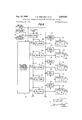
Filed April 26, 1962 A. H. BALLARD ETAL ORTHOGONAL POLYNOMIAL MULTIPLEX TRANSMISSION SYSTEMS 12 Sheets-Sheet 1 INFORMATION INPUT SIGNALS IHIII N sQuARE wAvE REFERENCE OSCILLATOR S|GNAL 3 CHANNEL I MULTIPLIER V CARRIER CHANNELH fi/4 I MULTIPLIER POLYNOMIAL CARRIER TRANSMITTING WAVEFORM 5 inm' fii sYNTI-IEsIzER F STATION CHANNELIII I MULTIPLIER V I CARRIER l I I O l I I f r I H EL N I C ANN MULTIPLIER 7 I CARRIER 9 a I WIRE OR RADIO COMPOSITE SIGNAL TRANsMIssIoN LINK AUTOMATIC H SYNC SIGNAL SYNCHRONIZER H MEMORY l5 CIRCUIT CHANNEL I SAMPLING WT r V I CORRELATION GATE 5;
F l2 [9 V I6 2O g CHANNEL II SAMPLING MEMORY CORRELATION GATE CIRCUIT 7) l3 I7 POLYNOMIAL RECEIVING w v CHANNELIII SAMPLING MEMORY m 8 STATION ANALYZER CORRELAMN GATE CIRCUIT 2 O '2 O 0 E O o O: o O 8 I4 '8 z H NNEL N SAMPLING MEMORY CORRELAHON GATE CIRCUIT INVENTORS fI-ff-E/ILLARD I BY 1965 A. H. BALLARD ETAL 3,204,034
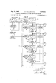
ORTHOGONAL POLYNOMIAL MULTIPLEX TRANSMISSION SYSTEMS Filed April 26, 1962 12 Sheets-Sheet 2 289 FIG. //A 290 SQUARE WAVE $1 SQUARE WAVE oScILLAToR I L I SYNC. SIGNAL DIFFERENTIATOR FREQUENCY MODULATOR 297 l FREQUENCY FULL-wAvE IMPULSE CONTROL 'NVERTER RECTIFIER 6 SYNG. SIGNAL SIGNAL SQUARE WAVE 298 w SYNc. SIGNAL 303 @308 4 3oo I I I 7 THRESHOLD SAMPLING MEMORY FREQUENCY H Po coNTRoL DIFFERENTIATOR DETECTOR GATE CIRCUIT SIGNAL COMPOSITE SIGNAL F OF FIGURE 2 299 302 304 306 INFORMATION INPUT SIGNALS I A w I 11 m N IMPULSE Q Q Q SYNc. SIGNAL I I SAMPLING SAMPLING SAMPLING SAMPLING O ll 2.IT GATE GATE GATE GATE 9 1 309 I, sIo I, 3" J, slz
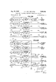
MEMORY MEMoRY MEMoRY MEMoRY 35 CIRCUIT l CIRCUIT CIRCUIT CIRCUIT 3I4 SIS SIG T0 T0 T0 T0 MULTIPLIER 3 MULTIPLIER 4 MULTIPLIER 5 MULTIPLIER 6 INVENTOR5 A.H.BALLARD B. R. BOY/MEL BY I P Aug. 31, 1965 A. H. BALLARD ETAL ORTHOGONAL POLYNOMIAL MULTIPLEX TRANSMISSION SYSTEMS Filed April 26, 1962 12 Sheets-Sheet 3 AAAAA VVVV COMPOSITE WAVEFORM ALTERNATE COMPOSITE WAVEFORM ALTERNATE COMPOSITE WAVEFORM A.H.BALLARD 5R BOY/MEL 1965 A. H. BALLARD ETAL 3,204,034
ORTHOGONAL POLYNOMIAL MULTIPLEX TRANSMISSION SYSTEMS Filed April 26, 1962 POWER POWER SPECTRUM OF WAVEFORM F IN FIGURE 2 FREQUENCY m I 3 5 7 9 Il I3 l5 l7 l9 2| 232527293| 3335 POWER 1.0-
POWER SPECTRUM OF WAVEFORM G IN FIGURE 2 7m FREQUENCY W m m m D V RL WME W AU 1 k A M 3. w 6 RH H UM EWZ Y P S m RNU ET E G U w n ml PWW mm 7 6 5 I34 R 2 M! I m. WW 0 M O O O Aug. 31, 1965 A. H. BALLARD ETAL 3,204,034
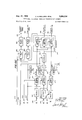
ORTHOGONAL POLYNOMIAL MULTIPLEX TRANSMISSION SYSTEMS Filed April 26, 1962 2 Sheets-Sheet 7 Aug. 31, 1965 A. H. BALLARD ETAL 3,204,034
ORTHOGONAL POLYNOMIAL MULTIPLEX TRANSMISSION SYSTEMS Filed April 26, 1962 12 Sheets-Sheet 8 PO F/G. 74 o EFERENCE P "7 w '23 a L V? P SIGNAL l INVERTING INVERTER J0 CHANNEL 1 AMPLIFIER I 0 CARRIER 2 mg NVERTER 1/5 Pg INVERTING I I I HANNEL T' AMPLIFIER L "2 I 1}?)ARRIER H 9 I I28 47p? 3 INVERTING INV 'PJcPT -CHANNEL1]I AMPLIFIER 1/?- 3 I M I CARRIER I20 I26 0 P I29 1/5 P4 4 INVERTING INVERTER W CHANNEL 11 H l2 AMPLIFIER 4 o W CARRIER I30 +1 04/ F/GI7B P W I59 1 PI REFERENCE l I INVERTING INVERTER SIGNAL 1 AMPLIFIER INVERTING INVERTER Ub CHANNEL 1 g- AMPLIFIER 1/5- PZ QQ CARRIER z/|45 7p? 5 INVERTING INVERTER CHANNEL 11 AMPLIFIER CARRIER P4 :/|46 P4 o4 INVERTING INVERTER W CHANNELDI v AMPLIFIER 1 4 W CARRIER I62 F P P P2 L SUMMING l INVERTING Lo REFERENCE INVERTER AMPLIFIER SIGNAL l6l ZI I54 fl (P3'PI) I49 MuLTI- INVERTING 0 I58 PLIER AMPLIFIER W I55 I CHANNEL I I63 2 CARRIER P3 P) SUMMING I0 3 I507 |NVERTER INVERTER W b I I I56 V (P INVERTING l4 0 M m I59 AMPLIFIER [I57 |64 CHANNEL 11 45 CARRIER P4 SUMMlNG T EWFPZ) INVERTER INVERTER [5| INVENTORS AHBALLARD '60 J) BY BRBmMEL ETC.
Aug. 31, 1965 Filed April 26, 1962 A. H. BALLARD ETAL ORTHOGONAL POLYNOMIAL MULTIPLEX TRANSMISSION SYSTEMS l2 Sheets-Sheet 9 IMPULSE F7639 SYNC. SIGNAL I85 SQUARE WAVE GAIN CONTROL SYNC. SIGNAL SIGNAL III |86 79 Et I67 I84 oMP%sIT:E AMPLIFIER RE/S/ET c SIGNAL F,G,OR H SWITCH I74 OF FIGURE2 //|68 V P m INTEGRATOR g MULTIPLIER f= RESET I69 SWITCH I75 I w -L- P (t) INTEeR IToR W1) MULTIPLIER I du Tof I88 /'L RESET SWITCH I76 I70 L y POLYNOMIAL l WAVEFORM P 0) lNTEGR/iTOR m SYNTHESIZER MULTIPLIER l 0F FIGURE '82 f du 7 4,5, OR 6 I89 RESET m SWITCH I77 I Y P 0) INTEGRATOR (i) MULTIPLIER I du RESET SWITCH I78 I72 /1/ =1 7 P 0) lNTEGR/iITOR M1) MULTIPLIER f du T K l I91 6 I73 ETC. ETC.
INVENTORS Aug. 31, 1965 A. H. BALLARD ETAL ORTHOGONAL POLYNOMIAL MULTIPLEX TRANSMISSION SYSTEMS Filed April 26, 1962 1,2 Sheets-Sheet ll F/ /0A l |C 2|8 2|9 20s 2I5 2|6 o INVERTER M V SAMPLING V MEMORY Jfi'fi ORflO( f) GATE CRCUIT SIGNAL 2|3 222 (V II) 'NVERT'NG i: cI-IANNEL I INVERTER A l b j CoRRELATIoN me 209 g 225 227 flv IIIoR p1 0) Im /g I r g CHANNEL 11 V? CORRELATION 2I4 M224 22s '13) lNVERTlNG CHANNEL 1]] L INVERTER :I fbg CORRELATION 2II a u) 229 (1) 0 21(1) W551 3 CHANNEL 11 V 1/? coRRELATIoN 245 250 m F/(i/OB 1 IO-1 W 255 Y u) OR SAMPLING MEMORY FREQUENCY f GATE CIRCUIT CONTROL g m SIGNAL I 25| 230249 252 GAIN I III 52235? SIGNAL 23? VIM INVERTING o INVERTER AM IER- mm V (I) OR 2 0) INVERTING ANNEL 1 AMPWITEIER MULTIPLIER CORRELATON 232 238 240 5 24? V 0) INVERTING CHANNELH V INVERTER f AM CORRELATION 253 $3) I 244 v 0) 0R I2 0) INVERTING CHANNEL 111 c i l- MULT'PL'ER CoRRELATIoN 242 INVENTORS A./7.BALLARD O ETC. 3. R BOY/MEL 1965 A. H. BALLARD ETAL 3,204,034
12 Sheets-Sheet l 2 v9 wt United States Patent 3,204,034 ORTHOGONAL POLYNOMIA'L MULTIPLEX TRANSMISSION SYSTEMS Arthur H. Ballard, 2001 N. Adams St., Arlington 1, Va.,
and Bernard R. Boymel, 5730 26th St. NW., Washington 15, DC.
Filed Apr. 26, 19'62, Ser. No. 190,294 9 Claims. '(Cl. 179-'15) This invention relates to systems for transmitting and receiving multiple channels of information signals over a single electrical or electromagnetic link. While not limited thereto, the information signals may consist of voice, music, telegraphy, telephoto, telemetering, remote control, or other signals.
Previously described multiplex transmission systems have employed either sine wave carriers separated in frequency, rectangular pulse carriers separated in time, or combinations thereof, to carry various information channels on a single transmission link in a form which permits the channels to be separated again without mutual interference. In the case of sine wave carriers, information has been conveyed by modulating the amplitude, frequency, or phase of the basic sine waves. In the case of rectangular pulse carriers, information has been conveyed by modulating the amplitude, duration, position, or group coding of the carrier pulses.
The use of sine wave carriers has the disadvantage that either a separate oscillator must be provided for each channel, or extremely complex equipment must be employed to generate harmonically related sine waves from a single oscillator. A further disadvantage is the inefficient utilization of bandwidth associated with sine wave carriers which results from the excessive frequency spacing between carriers needed in order that they can be separated without interference by resonant filter networks of practical design. Still another disadvantage is that the filter networks needed for channel separation often require the use of bulky components such as ironcore inductors, which results in an equipment of excessive size and weight.
The use of rectangular pulse carriers, on the other hand, has the disadvantage that complicated and frequently unreliable synchronizing equipment is needed to combine and separate the carrier pulses at proper instants of time. Related to this disadvantage is the everpresent hazard that improper synchronization will result in cross-connection of channels. A further disadvantage of pulse carrier systems is their lack of flexibility in increasing or decreasing the number of channels without major equipment changes.
The multiplex transmission systems of this invention obviate these limitations by the use of orthogonal polynomial signals. The term orthogonal is defined herein as the mutual property of two time-dependent waveforms, P (t) and P (t), such that their product averaged over a fixed time duration T, is equal to zero. That is to say, the two Waveforms are orthogonal if:
There are many sets of waveforms, all pairs of which satisfy the condition for orthogonality. The waveforms of concern to this invention are those which are polynomial functions of time. That is to say, all waveforms can be expressed as finite sums of algebraic terms, each term being a power of t, the independent time variable. A polynomial waveform of order n can be defined as:
"ice
where the quantities at; are fixed numerical coefficients.
The set of polynomial waveforms satisfying the orthogonality condition is unique except for arbitrary constant multiplying factors. These polynomials were, in fact, discovered by the French mathematician Legendre in the late eighteenth century, and are often referred to as Legendre polynomials. A theoretical discussion of these polynomials can be found, for example, in A Course of Modern Analysis by E. T. Wittaker and G. N. Watson, Cambridge University Press, 4th edition, reprinted 1958, pages 302-336.
It is one object of the present invention to provide a new class of multiplex transmission systems employing orthogonal polynomial waveforms as carrier signals, in order that many channels of electrical information can be combined on a single transmission link and separated again without mutual interference.
Another object of the present invention is to provide a class of multiplex transmission systems in which all channels share the same frequency spectrum and time duration in an efficient manner.
A further object of the present invention is to provide a class of multiplex transmission systems in which all channels provide equal amounts or rejection to random internal or external noise, such rejection being considerably higher than that exhibited by previous transmission systems.
Still another object of the present invention is to provide a class of multiplex transmission systems in which all channels are readily adaptable to proportional analog, as well as discrete digital modulation, the analog modulation being automatically calibrated, and being capable of either positive or negative excursions about a zero level, the zero level being automatically produced at the receiver in the event of signal interuption.
A still further object of the present invention is to provide a class of multiplex transmission systems which are readily adaptable to small, lightweight, reliable construction using solid-state components such as transistors, diodes, resistors, and capacitors.
Still another object of the present invention is to provide a class of multiplex transmission systems in which all channels are synchronized by a single oscillator, and in which the receiver is automatically and simply synchronized to the transmitter without danger of channel cross-connection.
A still further object of the present invention is to provide a class of multiplex transmission systems in which the number of channels can be'easily increased or decreased by adding or subtracting small amounts of equipment with little or no effect on the other channels.
Other objects and many of the attendant advantages of this invention will be readily appreciated as the same becomes better understood by reference to the following detailed description when considered in connection with the accompanying drawings, wherein:
FIGURE 1 is a block diagram illustrating a generalized embodiment of the class of multiplex transmission systems comprising the invention.
FIGURE 1A illustrates a modification of the information input circuits which may be used if bandwidth conservation is important.
FIGURE 2 illustrates the waveforms of the first five orthogonal polynomials, as well as three examples of composite transmission signals derived from the polynomial waveforms.
FIGURES 3A, 3B, and 3C are graphs of power spectrum vs. frequency for the composite signals of FIGURE 2.
FIGURE 4 is a block diagram of an electronic polynomial waveform synthesizer using cascaded integrator circuits.
FIGURE 5 is a block diagram of an electronic polynomial waveform synthesizer using cascaded multiplier circuits.
FIGURE 6 illustrates a polynomial waveform synthesizer using photoelectric techniques.
FIGURES 7A, 7B, and 7C show attachments for the synthesizer of FIGURES 4, 5, or 6 needed to obtain each of the composite signals of FIGURE 2.
FIGURE 8 is a block diagram of a polynomial waveform analyzer using the synthesizer of FIGURE 4, 5, or 6 in combination with a parallel bank of multiplier-integrator circuits.
FIGURE 9 is a block diagram of an electronic polynomial waveform analyzer using cascaded integrator circuits.
FIGURES 10A, 10B, and 10C show the attachments needed with the analyzer of FIGURES 8 or 9 for use with each of the composite waveforms of FIGURE 2.
FIGURE 11A is a block diagram illustrating one method of automatically producing suitable synchronizing signals at the receiving station.
FIGURE 11B is a block diagram illustrating one method of automatically deriving a frequency control signal at the receiving station from the composite signal F of FIGURE 2.
Overall operation of the multiplex transmission systems of this invention can be understood by referring to the block diagram of FIGURE 1. The equipment comprising the invention is divided into two parts-one part being located at the transmitting station, and the other part being located at the receiving station. The two stations may be remote from each other, the separation distance not being critical provided that they are connected by wire, radio, or other link capable of transmitting electrical signals. Either station, or both stations, may be located in moving vehicles if desired.
At the transmitting station, the carrier signals for each channel, as well as a reference signal, are derived from the output signal of a square wave oscillator 1 by means of a polynomial waveform synthesizer 2. The square wave oscillator 1 may be a conventional astable multivibrator such as described in the textbook Pulse and Digital Circuits by J. Millman and H. Taub, McGraw- Hill, 1956, at pages 199-201. The oscillator frequency is made at least equal to, and preferably greater than, the maximum bandwidth of the information signals to be transmitted. In typical applications of the invention, the square wave frequency might lie in the range from 10 cycles per second to 10 kilocycles per second, although these limits are not restrictive. The polynomial waveform synthesizer 2 can take various forms, several examples of which will be described later.
The carrier channels are labeled as I, II, III N in FIGURE 1 in order to make it very clear that the number of channels is not restricted; there being no fundamental limit to the number of channels other than the bandwidth available for transmission.
The carrier signals produced for each channel by the polynomial waveform synthesizer 2 are modulated with their corresponding information input signals by means of the multipliers 3, 4, 5, and 6. The information input signals are allowed to vary, in normalized form, anywhere within the range from 1 to +1. In typical applications of the invention, full scale information of +1 might represent a voltage in the range from 1 to 10 volts; although these limits are not restrictive. The multipliers 3, 4, 5, and 6 are of the four-quadrant type; that is they are capable of accepting either positive or negative signals at both input terminals and generating a product signal of correct algebraic polarity. In their simplest form, the multipliers 3, 4, 5, and 6 may consist of grounded-center-tap potentiometers, the carrier signals being applied with opposite polarity to the two ends of the potentiometers, and the information input signals being applied in the form of mechanical shaft rotations. Alternatively, the multipliers 3, 4, 5, and 6 may be entirely electronic devices as described for example in the paper A Transistorized Four Quadrant Time Division Multiplier With an Accuracy of 0.1 Percent by H. Schmid, IRE Transactions on Electronic Computers, March 1958, pages 41-47. The type of modulation produced by fourquadrant multiplication is equivalent to double-sideband, suppressed-carrier, amplitude modulation.
The modulated carriers for each channel, as well as an unmodulated reference signal are applied to a summing amplifier 7 which algebraically adds all signals together in a linear manner. The summing amplifier 7 may consist for example of a conventional operational amplifier and summing resistor network as described in the textbook Electronic Analog Computers, G. A. Korn and T. M. Korn, McGraw-Hill, 1952, at pages 12-14.
The composite signal produced by the summing amplifier 7 is transmitted over a wire or radio transmission link 8, which is not a part of this invention, to the receiving station. The transmission link 8 may possibly include additional modulation and demodulation equipment for placing the composite signal in an advantageous portion of the radio-frequency spectrum. The principal requirements on the transmission link 8 are that it be capable of producing a signal gain of approximately unity, that the noise level not be unreasonably high, and that the bandwidth be at least equal to the number of channels times the frequency of the square wave oscillator 1.
At the receiving station, the composite signal is applied to an automatic synchronizer 9, to be described later in detail in conjunction with FIGURE 11A. The purpose of this synchronizer is to detect automatically the fundamental frequency and phase of the square wave oscillator signal employed at the transmitting station and to generate noise-free synchronizing signals of the same frequency and phase for use at the receiving station.
The composite signal is also applied to a polynomial waveform analyzer 10, several possible forms of which will be described later in conjunction with FIGURES 8-10. The function of the polynomial waveform analyzer 10 is to compute, for each half cycle of the square Wave synchronizing signal, what value of information input signal was used to modulate each carrier. As will be shown, the computations performed are equivalent to correlating the composite signal with the carrier waveform for each channel. From the teachings of optimum signal detection in the presence of noise, as set forth for example in Random Signals and Noise, W. B. Davenport and W. L. Root, McGraw-Hill, 1958, pages 343- 345, it is known that correlation is the best process for measuring signal amplitudes with maximum rejection of noise.
At the end of each half cycle of the square wave synchronizing signal, the results of the correlation computation for each channel are passed through the sampling gates 11, 12, 13 and 14, and stored in the memory circuits 15, 16, 17, and 18. The sampling gates 11, 12, 13, and 14 may be conventional six-diode gates as described, for example, in Pulse and Digital Circuits, I. Millman and H. Taub, McGraw-Hill, 1956 at pages 445-447. Memory circuit 15 contains a memory capacitor 19, whose function is to store each sampled correlation voltage for channel I from one synchronizing interval to the next, and a lowpass filter 20, whose function is to produce an outward waveform which passes smoothly through the sequence of stored voltages. Memory circuits 16, 17, and 18 contain similar networks which perform the same functions for the other channels. Output signals taken from the memory circuits 15, 16, 17, and 18 represent the original information signals applied at the transmitting station.
In those applications where bandwidth conservation is important, the additional circuits shown in FIGURE 1A may be included in the transmitter equipment. It is essential that each information input signal remain constant, or very nearly constant, during each transmission interval in order that the carrier waveforms retain their orthogonal properties. This requirement is met if the frequency of the square wave synchronizing signal is large compared to the bandwidth of the information signals, but such a choice for the synchronizing frequency may be overly wasteful of bandwidth.
The well-known Nyquist Sampling Theorem teaches that any signal limited in bandwidth to a frequency f can be represented without loss of information by a series of sample values spaced at intervals or less. The circuits of FIGURE 1A permit a minimum sampling rate of samples per second to be employed, and consequently lead to a transmitted signal of minimum bandwidth.
The information input signals for channels I, II, III, and N are applied to sampling gates 309, 310, 311, and 312 respectively. Sampling gates 309, 310, 311, and 312 may be identical in design with those used in the receiving equipment of FIGURE 1. Also applied to the sampling gates 309, 310, 311, and 312, is an impulse synchronizing signal 313, which consists of sharp impulses at the end of each transmission interval. Synchronizing signal 313 may be derived from the output of square wave oscillator 1 as described later in connection with FIGURE 11A. The information samples are held constant for the next succeeding transmission interval by memory circuits 314, 315, 316, and 317, which may be similar to those used in the receiving circuits of FIG- URE 1, except that lowpass filtering is not used on the output of the memory capacitors.- The sampled and stored voltages taken from memory circuits 314, 315, 316, and 317 are applied to the multiplier circuits 3, 4, 5, and '6 respectively, in lieu of the original input information signals.
One of the principal unique features of the present invention is the use of carrier Waveforms which are orthogonal polynomial functions of time, or combinations thereof. Referring again to the theoretical discussion of orthogonal polynomials in A Course of Modern Analysis, E. T. Whittaker and G. N. Watson, Cambridge University Press, 4th edition reprinted 1958, pages 302-336, the first five polynomial functions which satisfy the orthogonality condition within a time duration T, are:
P (x) =2: Pm) P 00) (5x 3x) P 00) =%(35:c 30x +3) where x is a normalized independent variable defined as:
Higher order orthogonal polynomials can be derived from the two immediately lower order polynomials by either of the recurrence formulae:
Waveforms A, B, C. D, and E in FIGURE 2 illustrate the first five orthogonal polynomials P P P P and P respectively. Since all of the waveforms are derived 6 from the square wave A of FIGURE 2, they are shown with normal polarity during the time interval 0 to T, and with inverted polarity during the succeeding time interval T to 2T.
When using these orthogonal polynomial waveforms as carrier signals in a multi-channel link, multiplying factors must be applied if all carriers are to contain equal power in their fully modulated state. Equal power is desirable in order that no channel be more adversely affected by noise than any other. The power in each orthogonal polynomial waveform is proportional to:
f; P. (t)dtf P (x)da:- Therefore each polynomial P should be multiplied by the factor k /2n+1 to achieve equal power.
Waveform F of FIGURE 2 shows the composite signal obtained when the five waveforms A, B, C, D and E are properly weighted for equal power, modulated with +1 information signals, and added together. It will be noted that there is a discontinuous transition in waveform F at the end of each time interval T. This characteristic transition is useful for conveying synchronizing information, but may result in an undesirably broad frequency spectrum.
Waveform G of FIGURE 2 shows an alternate composite waveform obtained by omitting the P polynomial and allowing only the odd order polynomials to alternate in polarity from one synchronizing interval to the next. Waveform G typically exhibits a cusp at the transitions between synchronizing intervals and is more confined in frequency spectrum than waveform F.
Waveform H of FIGURE 2 shows another alternate composite waveform using difference waveforms as carrier signals. The weighting factors for equal power now become The cases n=0, 1 are omitted, and only the even order polynomials are allowed to alternate in polarity. Waveform H is continuous both in value and slope at the transitions between synchronizing intervals and is more confined in frequency spectrum than either waveform F or waveform G.
FIGURES 3A, 3B, and 3C illustrate the single-sided power spectra of the composite signals of FIGURE 2. Frequency is plotted only in the positive direction in terms of an index number, m representing harmonics of the fundamental square wave synchronizing frequency, 1/ 2T. If the composite signal is denoted by E (t), then its component of power at the mth harmonic frequency is:
When this computation is performed for composite signal F of FIGURE 2, the spectrum of FIGURE 3A is obtained, in which the power in the higher harmonics decreases with frequency in proportion to l/mP. Composite signal G of FIGURE 2 exhibits the spectrum of FIGURE 3B, in which power at high frequencies decreases in proportion to l/m"; and composite signal H of FIG- URE 2 exhibits the spectrum of FIGURE 3C, in which power of high frequencies decreases in proportion to l/m FIGURES 3A, 3B, and 3C clearly illustrate that from the standpoint of spectrum conservation, waveform G of FIGURE 2 is preferred to waveform F of FIG- URE 2, and waveform H of FIGURE 2 is preferred to either waveform F or G of FIGURE 2.
In FIGURES 3A, 3B, and 3C, a constant modulation of +1 has been assumed for all channels. As described earlier, a double-sideband, suppressed-carrier type of modulation is used. In the presence of time-varrying modula- 7 tion, the spectra of FIGURES 3A, 3B, and 3C would no longer be simple line spectra, but instead would consist of narrow bands of power symmetrically disposed about the harmonics of the synchronizing frequency.
Although only three examples of composite waveforms and their frequency spectra are illustrated in FIGURES 2 and 3, it should be clearly understood that other sets of carrier waveforms derivable from orthogonal polynomial signals are also included within the scope of the invention. For example, any set of carriers consisting of finite sums, differences, or products of orthogonal polynomials or other schemes of systematically changing polarity or other aspects of the orthogonal polynomials from one synchronizing interval to the next, do not violate the spirit or intent of this invention.
One of several possible methods of synthesizing orthogonal polynomial waveforms is illustrated in FIGURE 4. It makes use of cascaded integrator and adder circuits in accordance with the first recurrence formula cited earlier. When time is considered as the independent variable, this recurrence formula appears as follows:
Once the waveforms P (t) and P (t) are available, all other waveforms may be derived by repeated application of this formula.
In FIGURE 4, the square wave synchronizing signal 21 comprises the P (t) waveform since it has a constant value of +1 during its first half cycle. During its second half cycle, the square wave 21 has a constant value of l, and all waveforms derived from it will consequently be inverted in polarity.
The P (t) waveform 22 is derived by means of the integrator 23, which converts the square Wave 21 to a sawtooth wave 24, and the summing inverter 25, which adds the square wave 21 to the sawtooth wave 24, thereby making each half cycle of the P (t) waveform 22 symmetrical about the zero level. The integrator 23 consists of an operational amplifier and resistor-capacitor network as commonly used in analog computer applications and described, for example, in Electronic Analog Computers, G. A. Korn and T. M. Korn, McGraw-Hill, 1952, pages 138-146. The summing inverter 25 consists of a similar operational amplifier and a resistor network as described in the same textbook at pages 12-14.
At the end of each synchronizing interval, the impulse synchronizing signal 26 operates reset switch 27, causing integrator 23 to be reset to zero potential, thereby allow ing integrator 23 to operate independently from one synchronizing interval to the next. The impulse synchronizing signal 26 is derived from the square wave synchronizing signal 21 in a manner described later in connection with FIGURE 11A. Reset switch 27 may be a bi-directional diode switch as described in Pulse and Digital Circuits, J. Millman and H. Taub, McGraw-Hill, 1956, pages 438-440. A description of methods for resetting integrator 23 may be found in Electronic Analog Computers, G. A. Korn and T. M. Korn, McGraw-Hill, 1952, at pages 289-292.
In a similar manner, the P (t) sawtooth wave 22 is converted to the parabolic wave 28 by integrator 29. The P (t) waveform 30 is derived by means of the summing inverter 31, which adds a negative P (t), obtained from inverter 32, to the parabolic wave 28. Inverter 32 may be identical in design to the summing inverters 25 and 31, except that only one input terminal is used. It will be noted that the operations performed by integrator 29, inverter 32, and summing inverter 31 are precisely those prescribed by the recurrence formula given above, for the case of 12:2.
A further application of the recurrence formula yields the P (t) waveform 33. Integrator 34 converts the P (t) waveform to the cubic waveform 35, and inverter 36 and summing inverter 37 add the P (t) waveform with proper polarity. A still further application of the recurrence formula yields the P. (t) waveform 38. Integrator 39 converts the P (t) waveform to the quartic waveform 40, and inverter 41 and summing inverter 42 add the P (t) waveform with proper polarity. Additional orthogonal polynominal waveforms may be obtained if desired by cascading additional integrators, inverters, and summing inverters identical to those shown in FIGURE 4.
The reset switches 43, 44, and 45 are provided for resetting integrators 29, 34, and 39 respectively, to the zero level at the end of each synchronizing interval. Even though the integrated waveforms 28, 35, and 40 normally pass through the zero level at the end of each synchronizing interval, resetting is beneficial in that it counteracts the harmful effects of low-frequency noise and drift in the integrators 29, 34, and 39. An identical reset switch would be provided for each additional integrator employed in synthesizing higher order polynomial waveforms.
Another type of polynomial waveform synthesizer which may be used is shown in FIGURE 5. It makes use of cascaded multiplier and summing devices in accordance with the second recurrence formula cited earlier. With time as the dependent variable, this formula can be written as follows:
In FIGURE 5, the square wave synchronizing signal comprises the P (t) waveform, and the HO) waveform 56 is derived therefrom by means of integrator 57 and summing inverter 59, which operate in an identical manner to that already described in connection with FIGURE 4. Integrator 57is reset to zero potential by reset switch 58, in response to the impulse synchronizing signal 54.
The P (t) waveform 56 is applied to multiplier 60, to which is also applied the P (t) waveform 55. Multiplier 60 is an electronic four-quadrant multiplier of the type already described in connection with FIGURE 1. Its purpose is to rectify the alternations in polarity from one synchronizing interval to the next, of the P (t) waveform 56, so as to produce the repetitive sawtooth waveform 61. Inverter 62 produces the inverted sawtooth waveform 63. The inverted sawtooth waveform 63 is applied to the fourquadrant multipliers 64, 65, and 66, and any other multipliers used in generating additional carriers.
' as may be verified by setting n=2 in the recurrence formula cited above.
In similar fashion, multiplier 65 produces a product sig nal P (t)P (t), which is combined with the P (l) signal 56 in summing inverter 69. In summing inverter 69, weighting factors of 7 and /3 are applied to the P (t)P (t) and P (t) signals respectively, so as to produce the P (t) waveform 70.
FIGURE 6 depicts still another possible design for a polynomial waveform synthesizer It employs photoelectric techniques for generating polynomial waveforms of order two and higher. A conventional cathode ray tube 78 containing an electron gun assembly 79 energized by the high voltage power supply 80, is used to produce a finely-focused electron beam 81. A high frequency oscillator 82 driving a push-pull amplifier 83 applies a rapid sawtooth deflection voltage 84 to the vertical deflection 9 plates 85, causing the electron beam 81 to scan rapidly in a vertical direction.
At the same time, the electron beam is scanned in a horizontal direction by a low frequency sawtooth potentional applied to the horizontal deflection plates 86 by the push-pull amplifier 87. The sawtooth waveform applied to push-pull amplifier 87 is the P (t) polynomial waveform 88. It is generated from the P (t) square wave 89 as in FIGURES 4 and 5, by means of the integrator 90, reset switch 91, and summing inverter 92.
As the electron beam 81 strikes the phosphor screen 93, light is emitted which is either transmitted or blocked by the mask 94 depending upon the beam position. Separate apertures in the mask are shaped in accordance with each polynomial to be synthesized, horizontal displacement being portional to the independent variable x, and vertical height of the aperture being proportional to P,,(x) plus a constant bias sufiicient to avoid negative values. At each horizontal position x, the electron beam 81 scans rapidly in a vertical direction, the total amount of light passing through each aperture being proportional to its height.
To produce the carriers needed for composite Waveform F of FIGURE 2, the attachments shown in FIG- URE 7A are used in conjunction with the polynomial waveform synthesizer of FIGURES 4, 5, or 6. Input terminals 117, 118, 119, 120, and 121 of FIGURE 7A are connected to output terminals 46, 47, 48, 49, and 50 respectively of FIGURE 4; or to output terminals 73, 74, 75, 76, and 77 respectively of FIGURE or to output terminals 112, 113, 114, 115, and 116 respectively of FIGURE 6.
The P (t) waveform on input terminal 117 of FIG- URE 7A is available without further processing as a reference signal. The P (t) waveform on input terminal 118 is passed through inverting amplifier 112, where it is multiplied by a fixed factor of minus /3, and inverter 123 where it is further multiplied by a fixed factor of minus one. Both the inverting amplifier 122 and the inverter 123 may consist of an operational amplifier and resistor network as described in Electronic Analog Computers, G. A. Korn and T. M. Korn, McGraw-Hill, 1952, pages -12.
Output signals representing \/3P (t) and /3P (t) are available from inverter 123 and inverting amplifier 122 respectively, for use as the carrier signal for channel I. The weighting factor of \/3 assures that the channel I carrier, when fully modulated with a +1 information signal, will exhibit the same average power as the reference signal. The carrier signal is made available with both polarities to facilitate the four-quadrant multiplication process to be used in modulating the carrier.
In a similar manner, inverting amplifiers 124, 125, and 126; and inverters 127, 128, and 129 are used to derive carrier signals /5P (t), /7P (t), and i /9P (t) for channels II, III, and IV respectively.
FIGURE 7B shows the attachments to be used with FIGURES 4, 5, or 6 in producing the carrier signals needed for composite signal G of FIGURE 2. Input terminals 130, 131, 132, 133, and 134 of FIGURE 7B are connected to output terminals 46, 47, 48, 49, and 50 respectively of FIGURE 4; or to output terminals 73, 74, 75, 76, and 77 respectively of FIGURE 5; or to output terminals 112, 113, 114, 115, and 116 respectively of FIGURE 6.
The P (t) square wave appearing on terminal of FIGURE 7B is applied to the electronic multipliers 135 and 136. Multiplier 135 serves as a reversing switch to rectify the alternations in polarity from one synchronizing interval to the next, of the P t) polynomial Waveform appearing at terminal 132. Multiplier 136 performs the same function for the P (t) polynomial waveform appearing at terminal 134. Multipliers 135 and 136 may consist, for example, of the same electronic circuits for four-quadrant multiplication described in connection with FIGURE 1. Similar multipliers are used for each evenordered polynomial waveform.
It will be noted that when the attachments of FIGURE 7B are used with the synthesizer of FIGURE 6, the use of multipliers 135 and 136 in FIGURE 7B and multipliers 107 and 109 in FIGURE 6 is redundant, since the net result is to leave the P (t) and P (t) waveforms un changed. A simpler equipment is possible in this case if multipliers 107, 109, 135, and 136 are omitted, and the output signals of amplifiers 102 and 104 in FIGURE 6 tied directly to terminals 137 and 138 respectively in FIGURE 7B.
The remainder of the attachments in FIGURE 7B are similar to those in FIGURE 7A. Inverting amplifier 139 and inverter 140 produce a reference signal of the form /3P (t). In verting amplifiers 141, 142, and 143, and inverters 144, 145, and 146 produce carrier signals of the form 3/5150 i\/7 1 (t), and :vfigt for channels I, II, and III respectively.
The attachments shown in FIGURE 7C are used with the synthesizer of FIGURES 4, 5, or 6 to produce the carrier signals required for composite Waveform H of FIGURE 2. In this case, input terminals 147, 148, 149, 150, and 151 of FIGURE 7C are connected to output terminals 46, 47, 48, 49, and 50 respectively of FIGURE 4; or output terminals 73 74, 75, 76, and 77 respectively of FIGURE 5; or output terminals 112, 113, 114, 115, and 116 respectively of FIGURE 6.
The P (t) waveform appearing at terminal 147 of FIG- URE 7C is passed through inverter 152 and applied to the summing inverter 153. The P (t) waveform at terminal 149 is also supplied to summing inverter 153 such that a signal of the form is produced. In a similar manner, inverter 154 and summing inverter 155 are used to produce a signal of the form and inverter 156 and summing inverter 157 are used to produce a signal of the form It will be noted that when the attachments of FIGURE 7C are used with the synthesizer of FIGURE 4, a simplificatlon of equipment is possible. Signals of the form and are directly available at terminals 51, 52, and 53 respectively of FIGURE 4. In this case, the inverters 152, 154, and 156 and summing inverters 153, 155, and 157 of FIGURE 7C may be omitted, and the input terminals 158, 159, and 160 of FIGURE 7C may be connected directly to output terminals 51, 52, and 53 respectively of FIGURE 4.
In FIGURE 7C, the
waveform at terminal 159 is applied to multiplier 161, to which is also applied the P (t) waveform at terminal 147. Multiplier 161 serves to rectify the polarity alternations of the in the same way as described in connection with FIGURE 7B. Similar multiplier circuits Would be used for the same purpose for each additional order polynomial waveform.
Inverting amplifier 162 is used to obtain a reference signaal of the form Inverting amplifiers 163 and 164, and inverters 165 and 166, are used to obtain carrier signals of the form for channels I and II respectively.
After the carrier signals have been modulated and combined in the summing amplifier 7 of FIGURE 1, the composite signal for transmission, in the case of Waveform F of FIGURE 2, will have the form:
The coefficients a represent the modulating information input signals, which in normalized form, are allowed to vary anywhere in the range from 1 to +1. They are assumed to be varying slowly enough that they may be considered constant during any one time interval T. Although the formula above applies only to Waveform F of FIGURE 2 during the positive half-cycle of the synchronizing square Wave, the modifications of the formula necessary to describe waveform F of FIGURE 2 during the negative half-cycle, as well as Waveforms G and H of FIGURE 2 during both half-cycles, are readily apparent from the notations given in FIGURE 2.
At the receiving station, again for the case of waveform F of FIGURE 2,v the value of each modulation coefiicient a is determined by implementation of the formula:
This formula follows immediately from the orthogonality condition and the fact that each waveform /2n.-+lP (t) has a mean-square value of unity. Thus each modulation coefficient a can be computed by multiplying the composite signal E (t) by the normalized carrier for that channel, T /2n-{-1P (t), and integrating over the time duration These are the computations performed by the polynomial waveform analyzer portion of the invention. The analyzer is, as the formula for computing a indicates, a correlation device. According to the teachings of optimum signal detection, as set forth for example in Random Signals and Noise, W. B. Davenport and W. L. Root, Mc- Graw-Hill, 1958 at pages 343-345, correlation is the process which maximizes signal-to-noise ratio. The effective noise bandwidth of a correlation device is simply l/T, the reciprocal of the integrating time, or in this case twice the basic synchronizing frequency. Noise uniformly distributed in frequency spectrum is therefore rejected to the maximum possible extent by the receiving portion of the invention.
FIGURE 8 shows one possible design for a polynomial waveform analyzer capable *of performing the desired correlation computations. The composite signal received over the transmission link, which may have the form of either waveform F, G, or H of FIGURE 2 is applied to the amplifier 167. Amplifier 167 is a conventional linear amplifier whose gain is established by a control signal which is derived in a manner to be described later and applied to terminal 186. Amplifier 167 assures a net transmission gain of unity by compensating for any attenuation of the composite signal which might have occurred during transmission.
After passing through amplifier 167, the composite signal is applied to multipliers 168, 169, 170, 171, and 172, which may be similar circuits to those described in connection with FIGURE 1. Also applied to multipliers 168, 169, 170, 171, and 172 are the waveforms P 0), P (t), P (t), P (t), and P (t) obtained from the polynomial waveform synthesizer 173, which may be identical with the equipment shown in either FIGURES 4, 5, or 6. Synthesizer 173 is synchronized by the square Wave synchronizing signal 184 and impulse synchronizing signal 185, which are obtained at the receiver in a manner to be described later.
The product signals generated by multipliers 168, 169, 170, 171, and 172 are applied to integrators 174, 175, 176, 177, and 178, which may be identical circuits to those described in connection with FIGURE 4. At the end of each synchronizing interval, integrators 174, 175, 176, 177, and 178 are reset to the zero level by means of the impulse signal 185 and the reset switches 179, 180, 181, 182, and 183, also as described in connection with FIGURE 4.
The output signals from integrators 174, 175, 176, 177, and 178 are the correlation waveforms (t), (t), (t), t) and 5 0), which. are defined by the general formula:
It can be readily seen that, for the case of Waveform F of FIGURE 2, the value of each correlation waveform at the end of each synchronizing interval is proportional to the modulation coeflicient for that channel; that is:
The equipment needed to derive the coefficients a from the correlation waveforms ,,(t), for this case as well as the cases of waveforms G and H of FIGURE 2, is described later in connection with FIGURE 10.
FIGURE 9 shows an alternate design of a polynomial Waveform analyzer capable of performing the desired correlation computations. It employs cascaded integrator and summing circuits arranged to act as a multi-channel matched filter. With reference again to Random Signals and Noises, W. B. Davenport and W. L. Root, McGraw Hill, pages 244-247, a matched filter is another means of performing correlation computations, with the same degree of noise rejection.
In FIGURE 9, the composite signal received over the transmission link, which may have the form of either waveform F, G, or H of FIGURE 2, is applied to the linear amplifier 192. As described in connection with FIGURE 8, amplifier 192 and the gain control signal applied to terminal 193 assure a net transmission gain of unity.
The amplified composite signal is applied to multiplier 194, to which is also applied the square wave synchroniz- 13 ing signal 195. As described in connection with FIG- URES 7B and 7C, multiplier 194 serves to rectify the polarity alternations in the composite signal from one synchronizing interval to the next.
The polarity-corrected composite signal is then applied to integrator 196, which is reset at the end of each synchronizing interval by reset switch 197, in response to the impulse synchronizing signal 198. The output signal from integrator 196 is applied to the network 199, which is identical with the synthesizer equipment shown in FIG- URE 4, described in detail above.
The equipment consisting of integrator 196, its reset switch 197, and the network of cascaded integrators and summing inverters 199, comprise a multi-channel matched filter. A matched filter is defined as a network whose impulse response is equal to the desired signal waveform reversed in time. It will be noted that if all integrators are initially reset to zero, an impulse applied to integrator 196 will result in output signals at terminals 200, 201, 202, 203, and 204 which are precisely the polynomial waveforms P (t), P (t), P 0), P (t), and P (t) respectively, for the succeeding time duration T. The integrator 196 will convert an applied impulse into a unit step function at terminal 200. With a step function input, the network 199 will operate exactly the same as the polynomial waveform synthesizer of FIGURE 4.
The output signals arising when a composite signal E (t) is applied to integrator 196 is predictable by means of the well-known convolution theorem:
ao f mono-mm, ostsr In this formula, P,,(t) is the impulse response of the network at its nth output terminal, which has just been shown to be the nth order orthogonal polynomial waveform.
In the end of each synchronizing interval, the value of each output signal of FIGURE 9 is:
Since the time-reversed polynomial waveforms P (Tu) are unchanged if n is even, and changed only in sign if n is odd:
T t T)=(1) o E(u)P,,(u)du In the case of composite waveform F of FIGURE 2:
The output signals b (t), if sampled at the end of each synchronizing interval, are therefore proportional to the corresponding modulation coefficients a for each interval.
FIGURE A shows the attachments to be used with the polynomial waveform analyzer of either FIGURE 8 or 9 when the composite signal F of FIGURE 2 is transmitted. Output terminals 187, 188, 189, 190, and 191 of FIGURE 8 are connected to input terminals 208, 209, 210, 211, and 212 respectively of FIGURE 10A; or alternatively output terminals 200, 201, 202, 203, and 204 of FIGURE 9 are connected to input terminals 208, 213, 210, 214, and 212 respectively of FIGURE 10A.
Since either the (t) or 1/ 0) correlation waveform appearing at terminal 208 is produced with negative polarity, inverter 215 is used to obtain the desired positive polarity. The output from inverter 215 is applied to sampling gate 216, Where the impulse synchronizing signal 217 samples the modulation coefficient for the reference signal, a (T):- (T). The sequence of values for a is stored and filtered in memory circuit 218. Both the sampling gate 216 and memory circuit 218 may be identical with the circuits described in connection with FIG- URE 1.
Since the n coefficient had a constant value of +1 at the transmitter, the output signal 219 from memory circuit 218 will exhibit a constant average value representative of full-scale modulation. Output signal 219 may therefore be used as a gain control signal by connecting it either to terminal 186 of FIGURE 8 or to terminal 193 of FIGURE 9.
The inverting amplifiers 222, 223, 224, and 225 are used to apply the proper scaling factors /2 +1 to each correlation waveform. The output signals at terminals 226, 227, 228, and 229, if sampled at the end of each synchronizing interval, will produce the molulation coefficients a a a and a; respectively. Output terminals 226, 227, 228, and 229 are tied to the sampling gates of FIGURE 1 for this purpose.
The attachments of FIGURE 10B are used when composite signal G of FIGURE 2 is transmitted. In this case output terminals 187, 188, 189, 190, and 191 of FIGURE 8 are connected to input terminals 230, 231, 232, 233, and 234 respectively of FIGURE 10B; or alternatively output terminals 200, 201, 202, 203, and 204 of FIGURE 9 are connected to input terminals 230, 235, 232, 236, and 234 of FIGURE 10B.
As in FIGURE 10A, the inverters 237 and 238 of FIG- URE 10B are used to invert the odd order correlation waveforms obtained from FIGURE 9; and the inverting amplifiers 239, 240, 241, and 242 are used to apply scaling factors of -\/2n+l to each correlation waveform. In addition, the multipliers 243 and 244, operating in con junction with the square wave synchronizing signal 245, are required. Multipliers 243 and 244 serve to rectify the polarity alternations from one synchronizing interval to the next, of the correlation waveforms (t) and (t), or 1/ 0) and 1/ 0). A similar multiplier is required for each additional even order correlation waveform.
The output signals at terminals 246, 247, and 248, if sampled at the end of each synchronizing interval, will produce the modulation coefficients a a and a respectively. For this purpose, terminals 246, 247, and 248 are connected to the sampling gates of FIGURE 1.
In FIGURE 10B, a gain control signal is obtained from the output signal of inverting amplifier 239. The output of inverting amplifier 239 is applied to sampling gate 249 where it is sampled by the impulse synchronizing signal 250. Sampling gate 249 may be identical in design to those described in connection with FIGURE 1. The sequence of sampled values stored and filtered by memory circuit 251 represents the modulation coefiicient Since a had a constant value of +1 at the transmitter, the average voltage appearing at terminal 252 may be used as a gain control signal. Terminal 252 is tied either to terminal 186 of FIGURE 8 or to terminal 193 of FIGURE 9 for this purpose.
In a similar way, sampling gate 253 and memory circuit 254 may be used to obtain the average value of (T) or %(T). Since the zero order polynomial P (t) was not transmitted in this case, the average correlation (T) or %(T) will be zero if the receiver is operating in proper synchronism with the composite signal received. If the receiver is not properly synchronized, the average correlation value obtained will be:
If the time displacement A is positive, a negative correlation is obtained; and if the time displacement A is negative, a positive correlation is obtained. The signal ap- 15 pearing at terminal 255 may therefore be used as a frequency control signal as will be described later in connection with FIGURE 11.
FIGURE C shows the attachments to be used with FIGURE 8 or FIGURE 9 when the composite signal H of FIGURE 2 is transmitted. Output terminals 187, 188, 189, 190, and 191 of FIGURE 8 are connected to input terminals 256, 257, 258, 259, and 268 respectively of FIGURE 10C; or alternatively output terminals 201, 205, 206, and 207 of FIGURE 9 are connected to input terminals 261, 262, 263, and 264 respectively of FIGURE 10C.
The purpose of inverters 265, 266, and 267, and summing inverters 268, 269, and 27 0, is to produce correlation signals of the form [z( 0( We) '1( and N40) 2( These signals represent the correlation between the received composite signal and the carrier signals respectively.
When the polynomial waveform analyzer of FIGURE 9 is used, correlation signals of the form are immediately available at terminals 205, 206, and 207 of FIGURE 9. In this case the inverters 265, 266, and 267, and summing inverters 268, 269, and 270 of FIGURE 10C may be omitted. The
signal appearing at terminal 262 of FIGURE 10C is inverted in polarity by inverter 271, and the signal appearing at terminal 264 is inverted in polarity by inverter 272. Identical inverters would be used for additional even order correlation waveforms of FIGURE 9.
The odd order correlation waveforms, typified by the signal appearing at terminal 263 of FIGURE 10C, are of the correct polarity during the first half cycle of the synchronizing square wave 273, and of inverted polarity during the second half cycle. Multiplier 274, and similar multipliers for each additional odd order correlation signal, rectify the polarity alternations from one synchronizing interval to the next.
The decombiner 275 is required in this case because the reference and carrier signals are not orthogonal by themselves. If the decombiner 275 were not provided, the correlation computations at the receiver would produce the results:
To obtain the desired modulation coefiicients, the decombiner 275 makes use of the summing amplifiers 276, 27 7 and 278. Summing amplifiers 276, 277, and 278 may be similar in design to that described in connection with 16 FIGURE 1. Summing amplifier 276 produces a signal of the form:
which if sampled at the end of each synchronizing interval, will yield the modulation coefficient a Summing amplifier 277 produces a signal of the form:
which when sampled will yield the modulating coefficient a In the case illustrated, summing amplifier 277 acts only as an inverter with gain; however the addition of one more channel would require that a correlation signal be added with a suitable scale factor. Summing amplifier 278 produces a signal of the form:
which when sampled will yield the modulating coefiicient 1 In general, the decombiner derives each even order modulation coeflicient by forming a linear sum of all even order correlation waveforms, and derives each odd order modulation coefficient by forming a linear sum of all odd order correlation waveforms.
A gain control signal is obtained in this case by using the impulse synchronizing signal 279 to sample the output of summing amplifier 276 in sampling gate 280. The sequence of values for the a modulation coefiicient is stored and filtered in memory circuit 281. Since a had a constant value of +1 in this case, the average voltage appearing at terminal 282 may be used as a gain control signal by connecting it either to terminal 186 of FIGURE 8 or to terminal 193 of FIGURE 9.
The output signals appearing at terminals 283 and 284 of FIGURE 10C represent the correlation waveforms for channels I and II respectively, and are connected to the sampling gates of FIGURE 1 where the corresponding modulation coeflicients are derived.
A frequency control signal can be derived in this case from the (t) correlation waveform appearing at terminal 2-57 of FIGURE 10C, or alternatively from the 1,0 0) correlation waveform at terminal 261, after its polarity is inverted by inverter 285. The sampling gate 286, operating in response to the impulse synchronizing signal 279, and the memory circuit 287 are used to derive the correlation value (T) or ,b (T). When the receiver is properly synchronized an average result of zero will be obtained at terminal 288. If there is a positive time displacement of the receiver synchronizing signals relative to the composite signal received, a negative signal will appear at terminal 288; and if there is a negative time displacement, a positive signal will appear at terminal 288.
To assure that the receiver is operating in exact synchronism with the composite signal transmitted, the automatic synchrouizer shown in FIGURE 11A may be used. A square wave oscillator 289 is provided, which may be an astable multivibrator similar to that used at the transmitter. The square wave oscillator 289 produces the square wave synchronizing signal 290 which is required in the receiving equipment. In addition the square wave synchronizing signal 290 is passed through the diflierentia tor 291, which may be a passive resistor-capacitor circuit, to produce the waveform 292 which consists of impulses alternating in polarity. The waveform 292, as well as its inverse obtained from inverter 293, is applied to the fullwave rectifier 294. Full Wave rectifier 294, which may be a passive diode-resistor circuit, produces the impulse synchronizing signal 295 which is also required in the receiving equipment.
The frequency of the square wave oscillator 289 is
Claims (1)
- 4. THE METHOD OF MULTIPLE CHANNEL INTELLIGENCE COMMUNICATION WHICH COMPRISES GENERATING A PLURALITY OF WAVERFORMS BEARING A MUTUALLY ORTHOGONAL POLYNOMIAL RELATION TO EACH OTHER, AMPLITUDE MODULATING SAID WAVE FORMS WITH A PLURALITY OF INTELLIGENCE SIGNALS, COMBINING SAID MODULATED WAVEFORMS FOR TRANSMISSION, RECEIVING SAID COMBINED MODULATED WAVEFORMS, DERIVING A SYNCHRONIZING SIGNAL THEREFORM, CORRELATING THE COMPOSITE SIGNAL WITH THE ORTHOGONAL POLYNOMIAL WAVEFORM FOR EACH CHANNEL, SAMPLING THE CORRELATION WAVEFORM IN EACH CHENNEL, AND SMOOTHING THE SAMPLED CORRELATION WAVEFORM IN EACH CHANNEL FOR DERIVATION OF THE ORIGINAL INTELLIGENCE SIGNALS FOR UTILIZATION.
Priority Applications (1)
| Application Number | Priority Date | Filing Date | Title |
|---|---|---|---|
| US190294A US3204034A (en) | 1962-04-26 | 1962-04-26 | Orthogonal polynomial multiplex transmission systems |
Applications Claiming Priority (1)
| Application Number | Priority Date | Filing Date | Title |
|---|---|---|---|
| US190294A US3204034A (en) | 1962-04-26 | 1962-04-26 | Orthogonal polynomial multiplex transmission systems |
Publications (1)
| Publication Number | Publication Date |
|---|---|
| US3204034A true US3204034A (en) | 1965-08-31 |
Family
ID=22700750
Family Applications (1)
| Application Number | Title | Priority Date | Filing Date |
|---|---|---|---|
| US190294A Expired - Lifetime US3204034A (en) | 1962-04-26 | 1962-04-26 | Orthogonal polynomial multiplex transmission systems |
Country Status (1)
| Country | Link |
|---|---|
| US (1) | US3204034A (en) |
Cited By (33)
| Publication number | Priority date | Publication date | Assignee | Title |
|---|---|---|---|---|
| US3384715A (en) * | 1964-09-17 | 1968-05-21 | Mc Donnell Douglas Corp | Multiplex communication systems employing orthogonal hermite waveforms |
| US3432619A (en) * | 1963-07-31 | 1969-03-11 | Ibm | Random-access communication system employing pseudo-random signals |
| US3450840A (en) * | 1965-11-19 | 1969-06-17 | Ibm | Multiplex data transmission system using orthogonal transmission waveforms |
| US3649914A (en) * | 1967-11-14 | 1972-03-14 | Philips Corp | Suppressed carrier orthogonal modulation transmission device and associated transmitters and receivers for the transmission of synchronous pulse signals |
| US3720789A (en) * | 1969-07-28 | 1973-03-13 | Plessey Telecommunications Res | Electrical signalling systems using correlation detectors |
| US3746791A (en) * | 1971-06-23 | 1973-07-17 | A Wolf | Speech synthesizer utilizing white noise |
| US3795772A (en) * | 1972-05-01 | 1974-03-05 | Us Navy | Synchronization system for pulse orthogonal multiplexing systems |
| US4109208A (en) * | 1971-07-31 | 1978-08-22 | Nippon Gakki Seizo Kabushiki Kaisha | Waveform producing system |
| US4163258A (en) * | 1975-12-26 | 1979-07-31 | Sony Corporation | Noise reduction system |
| US4179586A (en) * | 1972-08-02 | 1979-12-18 | The United States Of America As Represented By The Secretary Of The Army | System of encoded speech transmission and reception |
| US4244053A (en) * | 1970-09-10 | 1981-01-06 | The United States Of America As Represented By The Secretary Of The Air Force | Privacy communication method and system |
| US4308614A (en) * | 1978-10-26 | 1981-12-29 | Fisher Charles B | Noise-reduction sampling system |
| US4390980A (en) * | 1981-07-27 | 1983-06-28 | Control Data Corporation | Demultiplexing plural data streams |
| US4550222A (en) * | 1981-09-28 | 1985-10-29 | Siemens Aktiengesellschaft | Process for interception-protected frequency band compressed transmission of speech signals |
| US4680777A (en) * | 1984-08-13 | 1987-07-14 | The University Of Michigan | Quadrature-quadrature phase shift keying |
| US4730344A (en) * | 1984-08-13 | 1988-03-08 | The University Of Michigan | Quadrature-quadrature phase shift keying with constant envelope |
| US4811357A (en) * | 1988-01-04 | 1989-03-07 | Paradyne Corporation | Secondary channel for digital modems using spread spectrum subliminal induced modulation |
| US4845749A (en) * | 1987-12-21 | 1989-07-04 | Bell Communications Research, Inc. | Secure teleconferencing system |
| US4920565A (en) * | 1988-07-18 | 1990-04-24 | Northern Telecom Limited | Method for connection of secure conference calls |
| US5001723A (en) * | 1985-11-05 | 1991-03-19 | Allied-Signal Inc. | Sinusoidal M-ary orthogonal keyed decoding |
| US5228055A (en) * | 1991-01-31 | 1993-07-13 | Clarion Co., Ltd. | Spread spectrum communication device |
| WO1996002101A1 (en) * | 1994-07-12 | 1996-01-25 | Usa Digital Radio Partners L.P. | Method and system for simultaneously broadcasting and receiving digital and analog signals |
| US5500898A (en) * | 1995-03-31 | 1996-03-19 | Nec Corporation | Scramble communication system multiplexing/demultiplexing scramble generation polynomial |
| US20050056140A1 (en) * | 2003-06-02 | 2005-03-17 | Nam-Ik Cho | Apparatus and method for separating music and voice using independent component analysis algorithm for two-dimensional forward network |
| US20150303567A1 (en) * | 2014-04-18 | 2015-10-22 | Raytheon Company | Beam forming system having linear samplers |
| WO2016124841A1 (en) | 2015-02-03 | 2016-08-11 | Commissariat A L'energie Atomique Et Aux Energies Alternatives | Method and device for phase modulation of a carrier wave and application to the detection of multi-level phase-encoded digital signals |
| US20170063591A1 (en) * | 2015-09-02 | 2017-03-02 | Astrapi Corporation | Spiral polynomial division multiplexing |
| US10686635B2 (en) | 2015-09-02 | 2020-06-16 | Astrapi Corporation | Spiral polynomial division multiplexing |
| US10931403B2 (en) | 2019-05-15 | 2021-02-23 | Astrapi Corporation | Communication devices, systems, software and methods employing symbol waveform hopping |
| US11184201B2 (en) | 2019-05-15 | 2021-11-23 | Astrapi Corporation | Communication devices, systems, software and methods employing symbol waveform hopping |
| US11228477B2 (en) | 2019-03-06 | 2022-01-18 | Astrapi Corporation | Devices, systems, and methods employing polynomial symbol waveforms |
| US11310090B2 (en) | 2016-05-23 | 2022-04-19 | Astrapi Corporation | Systems, transmitters, and methods employing waveform bandwidth compression to transmit information |
| US11824694B2 (en) | 2015-09-02 | 2023-11-21 | Astrapi Corporation | Systems, devices, and methods employing instantaneous spectral analysis in the transmission of signals |
Citations (2)
| Publication number | Priority date | Publication date | Assignee | Title |
|---|---|---|---|---|
| US3025350A (en) * | 1957-06-05 | 1962-03-13 | Herbert G Lindner | Security communication system |
| US3036157A (en) * | 1960-05-09 | 1962-05-22 | Gen Dynamics Corp | Orthogonal function communication system |
-
1962
- 1962-04-26 US US190294A patent/US3204034A/en not_active Expired - Lifetime
Patent Citations (2)
| Publication number | Priority date | Publication date | Assignee | Title |
|---|---|---|---|---|
| US3025350A (en) * | 1957-06-05 | 1962-03-13 | Herbert G Lindner | Security communication system |
| US3036157A (en) * | 1960-05-09 | 1962-05-22 | Gen Dynamics Corp | Orthogonal function communication system |
Cited By (41)
| Publication number | Priority date | Publication date | Assignee | Title |
|---|---|---|---|---|
| US3432619A (en) * | 1963-07-31 | 1969-03-11 | Ibm | Random-access communication system employing pseudo-random signals |
| US3384715A (en) * | 1964-09-17 | 1968-05-21 | Mc Donnell Douglas Corp | Multiplex communication systems employing orthogonal hermite waveforms |
| US3450840A (en) * | 1965-11-19 | 1969-06-17 | Ibm | Multiplex data transmission system using orthogonal transmission waveforms |
| US3649914A (en) * | 1967-11-14 | 1972-03-14 | Philips Corp | Suppressed carrier orthogonal modulation transmission device and associated transmitters and receivers for the transmission of synchronous pulse signals |
| US3720789A (en) * | 1969-07-28 | 1973-03-13 | Plessey Telecommunications Res | Electrical signalling systems using correlation detectors |
| US4244053A (en) * | 1970-09-10 | 1981-01-06 | The United States Of America As Represented By The Secretary Of The Air Force | Privacy communication method and system |
| US3746791A (en) * | 1971-06-23 | 1973-07-17 | A Wolf | Speech synthesizer utilizing white noise |
| US4109208A (en) * | 1971-07-31 | 1978-08-22 | Nippon Gakki Seizo Kabushiki Kaisha | Waveform producing system |
| US3795772A (en) * | 1972-05-01 | 1974-03-05 | Us Navy | Synchronization system for pulse orthogonal multiplexing systems |
| US4179586A (en) * | 1972-08-02 | 1979-12-18 | The United States Of America As Represented By The Secretary Of The Army | System of encoded speech transmission and reception |
| US4163258A (en) * | 1975-12-26 | 1979-07-31 | Sony Corporation | Noise reduction system |
| US4308614A (en) * | 1978-10-26 | 1981-12-29 | Fisher Charles B | Noise-reduction sampling system |
| US4390980A (en) * | 1981-07-27 | 1983-06-28 | Control Data Corporation | Demultiplexing plural data streams |
| US4550222A (en) * | 1981-09-28 | 1985-10-29 | Siemens Aktiengesellschaft | Process for interception-protected frequency band compressed transmission of speech signals |
| US4680777A (en) * | 1984-08-13 | 1987-07-14 | The University Of Michigan | Quadrature-quadrature phase shift keying |
| US4730344A (en) * | 1984-08-13 | 1988-03-08 | The University Of Michigan | Quadrature-quadrature phase shift keying with constant envelope |
| US5001723A (en) * | 1985-11-05 | 1991-03-19 | Allied-Signal Inc. | Sinusoidal M-ary orthogonal keyed decoding |
| US4845749A (en) * | 1987-12-21 | 1989-07-04 | Bell Communications Research, Inc. | Secure teleconferencing system |
| US4811357A (en) * | 1988-01-04 | 1989-03-07 | Paradyne Corporation | Secondary channel for digital modems using spread spectrum subliminal induced modulation |
| US4920565A (en) * | 1988-07-18 | 1990-04-24 | Northern Telecom Limited | Method for connection of secure conference calls |
| US5228055A (en) * | 1991-01-31 | 1993-07-13 | Clarion Co., Ltd. | Spread spectrum communication device |
| WO1996002101A1 (en) * | 1994-07-12 | 1996-01-25 | Usa Digital Radio Partners L.P. | Method and system for simultaneously broadcasting and receiving digital and analog signals |
| US5500898A (en) * | 1995-03-31 | 1996-03-19 | Nec Corporation | Scramble communication system multiplexing/demultiplexing scramble generation polynomial |
| US20050056140A1 (en) * | 2003-06-02 | 2005-03-17 | Nam-Ik Cho | Apparatus and method for separating music and voice using independent component analysis algorithm for two-dimensional forward network |
| US7122732B2 (en) * | 2003-06-02 | 2006-10-17 | Samsung Electronics Co., Ltd. | Apparatus and method for separating music and voice using independent component analysis algorithm for two-dimensional forward network |
| US20150303567A1 (en) * | 2014-04-18 | 2015-10-22 | Raytheon Company | Beam forming system having linear samplers |
| US9577328B2 (en) * | 2014-04-18 | 2017-02-21 | Raytheon Company | Beam forming system having linear samplers |
| US10341150B2 (en) | 2015-02-03 | 2019-07-02 | Commissariat A L'energie Atomique Et Aux Energies Alternatives | Method and device for phase modulation of a carrier wave and application to the detection of multi-level phase-encoded digital signals |
| WO2016124841A1 (en) | 2015-02-03 | 2016-08-11 | Commissariat A L'energie Atomique Et Aux Energies Alternatives | Method and device for phase modulation of a carrier wave and application to the detection of multi-level phase-encoded digital signals |
| US10686635B2 (en) | 2015-09-02 | 2020-06-16 | Astrapi Corporation | Spiral polynomial division multiplexing |
| US10069664B2 (en) * | 2015-09-02 | 2018-09-04 | Astrapi Corporation | Spiral polynomial division multiplexing |
| US20170063591A1 (en) * | 2015-09-02 | 2017-03-02 | Astrapi Corporation | Spiral polynomial division multiplexing |
| US10972322B2 (en) | 2015-09-02 | 2021-04-06 | Astrapi Corporation | Spiral polynomial division multiplexing |
| US11411785B2 (en) | 2015-09-02 | 2022-08-09 | Astrapi Corporation | Spiral polynomial division multiplexing |
| US11824694B2 (en) | 2015-09-02 | 2023-11-21 | Astrapi Corporation | Systems, devices, and methods employing instantaneous spectral analysis in the transmission of signals |
| US11310090B2 (en) | 2016-05-23 | 2022-04-19 | Astrapi Corporation | Systems, transmitters, and methods employing waveform bandwidth compression to transmit information |
| US11228477B2 (en) | 2019-03-06 | 2022-01-18 | Astrapi Corporation | Devices, systems, and methods employing polynomial symbol waveforms |
| US11729041B2 (en) | 2019-03-06 | 2023-08-15 | Astrapi Corporation | Devices, systems, and methods employing polynomial symbol waveforms |
| US10931403B2 (en) | 2019-05-15 | 2021-02-23 | Astrapi Corporation | Communication devices, systems, software and methods employing symbol waveform hopping |
| US11184201B2 (en) | 2019-05-15 | 2021-11-23 | Astrapi Corporation | Communication devices, systems, software and methods employing symbol waveform hopping |
| US11582075B2 (en) | 2019-05-15 | 2023-02-14 | Astrapi Corporation | Communication devices, systems, software and methods employing symbol waveform hopping |
Similar Documents
| Publication | Publication Date | Title |
|---|---|---|
| US3204034A (en) | Orthogonal polynomial multiplex transmission systems | |
| Nichols et al. | Radio telemetry | |
| US3500215A (en) | Filter for bivalent pulse signals | |
| USRE23686E (en) | Communication system | |
| US3204035A (en) | Orthonormal pulse multiplex transmission systems | |
| GB859002A (en) | Improvements in or relating to phase modulators for carrier communication systems | |
| US3525941A (en) | Stepwave converter | |
| US3030614A (en) | Telemetry system | |
| US4152772A (en) | Apparatus for performing a discrete cosine transform of an input signal | |
| US3025350A (en) | Security communication system | |
| US4205241A (en) | Quantized modulation systems | |
| US3032745A (en) | Data transmission system | |
| US3095539A (en) | Digitally positioned wave filter | |
| GB843406A (en) | Improvements relating to signal-translating apparatus | |
| US3689750A (en) | Phase-independent digital correlator for use in radar systems | |
| US2736007A (en) | Teledata system | |
| US3090953A (en) | Pulse burst compression radar | |
| CA1121503A (en) | Surface elastic wave hadamar transformer | |
| US3456199A (en) | Two level to three level pulse code converter utilizing modulo-2 logic and delayed pulse feedback | |
| GB919161A (en) | Amplitude modulation system | |
| US2619632A (en) | Pulse communication system | |
| US2629017A (en) | Speech transmission system | |
| US3541266A (en) | Bandwidth compressor and expander | |
| US2900459A (en) | Single sideband amplifier | |
| US3057555A (en) | Electronic computer |