US3649837A - Diffractive image-forming means integrated into semiconducting devices - Google Patents
Diffractive image-forming means integrated into semiconducting devices Download PDFInfo
- Publication number
- US3649837A US3649837A US32160A US3649837DA US3649837A US 3649837 A US3649837 A US 3649837A US 32160 A US32160 A US 32160A US 3649837D A US3649837D A US 3649837DA US 3649837 A US3649837 A US 3649837A
- Authority
- US
- United States
- Prior art keywords
- zone plate
- radiation
- forming means
- photoelectric device
- photoelectric
- Prior art date
- Legal status (The legal status is an assumption and is not a legal conclusion. Google has not performed a legal analysis and makes no representation as to the accuracy of the status listed.)
- Expired - Lifetime
Links
- 230000005855 radiation Effects 0.000 claims abstract description 32
- 230000004888 barrier function Effects 0.000 claims description 37
- 230000005669 field effect Effects 0.000 claims description 6
- 239000011248 coating agent Substances 0.000 claims description 4
- 238000000576 coating method Methods 0.000 claims description 4
- 239000007787 solid Substances 0.000 claims description 3
- 230000003287 optical effect Effects 0.000 abstract description 12
- 230000010354 integration Effects 0.000 abstract description 7
- 229910052710 silicon Inorganic materials 0.000 description 12
- 239000010703 silicon Substances 0.000 description 11
- XUIMIQQOPSSXEZ-UHFFFAOYSA-N Silicon Chemical compound [Si] XUIMIQQOPSSXEZ-UHFFFAOYSA-N 0.000 description 10
- 229910052751 metal Inorganic materials 0.000 description 10
- 239000002184 metal Substances 0.000 description 10
- 239000004065 semiconductor Substances 0.000 description 9
- 238000005286 illumination Methods 0.000 description 8
- PCHJSUWPFVWCPO-UHFFFAOYSA-N gold Chemical compound [Au] PCHJSUWPFVWCPO-UHFFFAOYSA-N 0.000 description 5
- 239000010931 gold Substances 0.000 description 4
- 229910052737 gold Inorganic materials 0.000 description 4
- 239000000463 material Substances 0.000 description 4
- 229910001218 Gallium arsenide Inorganic materials 0.000 description 3
- 239000002019 doping agent Substances 0.000 description 3
- 230000010363 phase shift Effects 0.000 description 3
- 230000009471 action Effects 0.000 description 2
- 230000000903 blocking effect Effects 0.000 description 2
- 230000001427 coherent effect Effects 0.000 description 2
- 230000006870 function Effects 0.000 description 2
- BASFCYQUMIYNBI-UHFFFAOYSA-N platinum Chemical compound [Pt] BASFCYQUMIYNBI-UHFFFAOYSA-N 0.000 description 2
- 239000000758 substrate Substances 0.000 description 2
- 239000012780 transparent material Substances 0.000 description 2
- ZXEYZECDXFPJRJ-UHFFFAOYSA-N $l^{3}-silane;platinum Chemical compound [SiH3].[Pt] ZXEYZECDXFPJRJ-UHFFFAOYSA-N 0.000 description 1
- 238000010521 absorption reaction Methods 0.000 description 1
- 229910052782 aluminium Inorganic materials 0.000 description 1
- XAGFODPZIPBFFR-UHFFFAOYSA-N aluminium Chemical compound [Al] XAGFODPZIPBFFR-UHFFFAOYSA-N 0.000 description 1
- 229910052785 arsenic Inorganic materials 0.000 description 1
- 230000015572 biosynthetic process Effects 0.000 description 1
- 239000000969 carrier Substances 0.000 description 1
- 239000000470 constituent Substances 0.000 description 1
- 239000013078 crystal Substances 0.000 description 1
- 238000000151 deposition Methods 0.000 description 1
- 230000009977 dual effect Effects 0.000 description 1
- 238000005516 engineering process Methods 0.000 description 1
- 239000011521 glass Substances 0.000 description 1
- 239000012535 impurity Substances 0.000 description 1
- 238000000206 photolithography Methods 0.000 description 1
- 229910052697 platinum Inorganic materials 0.000 description 1
- 229910021339 platinum silicide Inorganic materials 0.000 description 1
- 230000004044 response Effects 0.000 description 1
- 230000002441 reversible effect Effects 0.000 description 1
- 238000007493 shaping process Methods 0.000 description 1
Images
Classifications
-
- H—ELECTRICITY
- H01—ELECTRIC ELEMENTS
- H01L—SEMICONDUCTOR DEVICES NOT COVERED BY CLASS H10
- H01L31/00—Semiconductor devices sensitive to infrared radiation, light, electromagnetic radiation of shorter wavelength or corpuscular radiation and specially adapted either for the conversion of the energy of such radiation into electrical energy or for the control of electrical energy by such radiation; Processes or apparatus specially adapted for the manufacture or treatment thereof or of parts thereof; Details thereof
-
- G—PHYSICS
- G03—PHOTOGRAPHY; CINEMATOGRAPHY; ANALOGOUS TECHNIQUES USING WAVES OTHER THAN OPTICAL WAVES; ELECTROGRAPHY; HOLOGRAPHY
- G03F—PHOTOMECHANICAL PRODUCTION OF TEXTURED OR PATTERNED SURFACES, e.g. FOR PRINTING, FOR PROCESSING OF SEMICONDUCTOR DEVICES; MATERIALS THEREFOR; ORIGINALS THEREFOR; APPARATUS SPECIALLY ADAPTED THEREFOR
- G03F7/00—Photomechanical, e.g. photolithographic, production of textured or patterned surfaces, e.g. printing surfaces; Materials therefor, e.g. comprising photoresists; Apparatus specially adapted therefor
- G03F7/70—Microphotolithographic exposure; Apparatus therefor
- G03F7/70383—Direct write, i.e. pattern is written directly without the use of a mask by one or multiple beams
-
- H—ELECTRICITY
- H01—ELECTRIC ELEMENTS
- H01L—SEMICONDUCTOR DEVICES NOT COVERED BY CLASS H10
- H01L27/00—Devices consisting of a plurality of semiconductor or other solid-state components formed in or on a common substrate
-
- H—ELECTRICITY
- H01—ELECTRIC ELEMENTS
- H01L—SEMICONDUCTOR DEVICES NOT COVERED BY CLASS H10
- H01L27/00—Devices consisting of a plurality of semiconductor or other solid-state components formed in or on a common substrate
- H01L27/14—Devices consisting of a plurality of semiconductor or other solid-state components formed in or on a common substrate including semiconductor components sensitive to infrared radiation, light, electromagnetic radiation of shorter wavelength or corpuscular radiation and specially adapted either for the conversion of the energy of such radiation into electrical energy or for the control of electrical energy by such radiation
- H01L27/144—Devices controlled by radiation
- H01L27/1443—Devices controlled by radiation with at least one potential jump or surface barrier
-
- H—ELECTRICITY
- H01—ELECTRIC ELEMENTS
- H01L—SEMICONDUCTOR DEVICES NOT COVERED BY CLASS H10
- H01L31/00—Semiconductor devices sensitive to infrared radiation, light, electromagnetic radiation of shorter wavelength or corpuscular radiation and specially adapted either for the conversion of the energy of such radiation into electrical energy or for the control of electrical energy by such radiation; Processes or apparatus specially adapted for the manufacture or treatment thereof or of parts thereof; Details thereof
- H01L31/12—Semiconductor devices sensitive to infrared radiation, light, electromagnetic radiation of shorter wavelength or corpuscular radiation and specially adapted either for the conversion of the energy of such radiation into electrical energy or for the control of electrical energy by such radiation; Processes or apparatus specially adapted for the manufacture or treatment thereof or of parts thereof; Details thereof structurally associated with, e.g. formed in or on a common substrate with, one or more electric light sources, e.g. electroluminescent light sources, and electrically or optically coupled thereto
-
- H—ELECTRICITY
- H01—ELECTRIC ELEMENTS
- H01L—SEMICONDUCTOR DEVICES NOT COVERED BY CLASS H10
- H01L33/00—Semiconductor devices with at least one potential-jump barrier or surface barrier specially adapted for light emission; Processes or apparatus specially adapted for the manufacture or treatment thereof or of parts thereof; Details thereof
Definitions
- ABSTRACT Integrated electro-optical structures are disclosed which comprise a difiractive image-forming means on a transparent semiconductive body in optical alignment with a photoelectric element on said body.
- image-forming means and photoelectrical element are located at the same surface of said body and radiation passes between them by reflection on the opposite surface of the body. This arrangement permits extensive electric integration of conducting portions of image-forming means with a photoelectric device.
- This invention concerns the integration of certain devices of the broad class of photoelectric devices as defined in my application Ser. No. 653,245, now U.S. Pat. No. 3,569,997, with a diffractive image-forming means, whereby both photoelectric device and imageforming means are located at a surface of a transparent semiconducting body.
- This body has the dual function of optical spacing of photoelectric device from image-forming means and of electric element for the semiconducting device.
- the photoelectric devices of this invention are photocells and/or light emitters. Because of the well-known reversibility of direction of radiation with respect to image-forming means, for each inventive arrangement of a photocell with respect to a diffractive optical means there exists a corresponding arrangement involving a light emitter replacing the photocell.
- the photoelectric devices In order that the semiconducting body is transparent to the radiation in question, the photoelectric devices must be active with respect to radiation of a wavelength which is longer than that corresponding to the absorption edge of the semiconducting body. This is achieved by using Schottky barrier diodes as photocells and heterojunctions between the semiconducting body and another semiconductor of smaller band gap as light emitters and/or photocells.
- the diffractive image-forming means can be located (i) at the same surface of the transparent body as the photoelectric device, or else (ii) at the opposite surface; as illustrated in FIG. 9 of my application Ser. No. 653,245, now U.S. Patent No. 3,569,997, or else (iii) at a surface substantially at right angles from the photoelectric device, the location at the same surface offers particular advantages for planar technology processing, for precise alignment between imageforrning means and photoelectric device, and for electric integration of portions of the zone plate with the photoelectric device or associated circuitry.
- the back surface is utilized as a mirror for radiation passing from imageforming means to photoelectric device.
- Highly integrated structures are made by using conducting segments of the zone plate as electrical contacts to photocell and to an associated amplifier, or by using these segments as contacts to a multiplicity of photocells enabling sensing of the off-axis position of an object.
- FIG. 1 shows a heterojunction light emitter integrated with a zone plate optics located at the same surface of a transparent body.
- FIG. 2 shows a Schottky barrier photocell integrated with a zone plate optics located at the same surface of a transparent semiconducting body.
- FIG. 3 shows photocell and zone plate optics of FIG. 2 integrated electrically with a bipolar transistor amplifier for the photocell current.
- FIG. 4 shows photocell and zone plate optics of FIG. 2 integrated electrically with an insulated gate field effect transistor.
- FIG. 5 shows various sections of a zone plate optics used as Schottky barrier contacts for registration of angle of incidence of radiation with respect to the optical axis of the zone plate.
- FIG. 6 shows a zone plate optics located at a first surface of a transparent semiconducting body and focusing radiation on a Schottky barrier photocell located at another surface of said body.
- FIG. 7 shows an ovonic switch integrated with a zone plate optics according to this invention.
- a Schottky barrier contact is a metal contact to a semiconductor causing a depletion region of majority carriers in the adjacent semiconductor.
- Schottky barriers arise by suitable choice of the metal (in particular, its work function) in combination with a suitable semiconducting material containing appropriate dopant impurities. For instance, in the case of a gold electrode to N- type silicon of about l0' /cc. dopant concentration, electrons leaving the gold and entering the conduction band of silicon have to overcome an energy step of 0.8 electron volt, while electrons leaving the valence band and entering the gold have to acquire an energy of 0.3 electron volt. Gold forms a Schottky barrier with P-type silicon if the dopant concentration is sufficiently large that the Fermi level in the bulk of the silicon is above the valence band by less than 0.3 electron volt.
- Another well-known means of producing a Schottky barrier to silicon consists of platinum heated in contact with silicon to about 550 C. to produce platinum silicide.
- Aluminum to N-type GaAs forms a Schottky barrier contact of about 0.8 electron volt barrier height.
- the electron flow from a negatively biased Schottky barrier contact into the semiconductor is limited by emission rate of electrons from the metal over the barrier.
- the emission current is enhanced greatly by illumination of the metal with light of a sufficiently short wavelength that its photon energy is larger than the barrier height.
- a Schottky barrier acts as a photocell.
- the metal is illuminated through the semiconducting body.
- l-leterojunctions are boundaries between two semiconducting materials of somewhat different band gap.
- Well-known examples are mixed crystals of Ge-Si, or else GaAs-Ga? differing in the concentration of the constituents at either side of the junction.
- Light emitted from the shorter band gap material of a forward biased PN heterojunction penetrates readily the wider band gap material, e.g., GaAs-light emission penetrates Gal.
- the height of the transparent rings providing a phase shift of 1r, and the thickness of the opaque metal rings are of the order of 0.1 to 1 micron.
- the thickness of a transparent semiconducting wafer is typically of the order of 200 microns.
- zone plate This is a very convenient order of magnitude for standard semiconductor photolithography processing.
- spacing the zone plate from underlying semiconductor surface by a transparent insulating layer of only I micron thickness would require comparatively small ring distances, if the zone plate were designed to focus on a photoelectric element located at said surface of the semiconducting body.
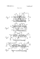
- FIG. 1 there is shown in cross section a semiconducting body 1 of N-type GaAs -,P having on its upper surface 2 an overlayed P-type GaAs layer .3.
- Contact leads 4 and 5 connect to battery 6 and bias the PN heterojunction 12 between 3 and l in the forward direction.
- Light emitted from the heterojunction into the body 1 is reflected on the reflecting metal coating 7 located at the back surface 8 of 1 and is emitted through front surface 2, which has ringshaped grooves 9, 10, 11 appropriately chosen in location, width and depth to represent a zone plate optics 14 for the radiation emitted from 12, so that a plane parallel outgoing beam 13 is formed.
- FIG. 2 shows a similar arrangement for a photocell exposed to incident coherent monochromatic radiation 22.
- N-type silicon body 21 shown in cross section carries the Schottky barrier contact 15 which represents also the central, opaque region of zone plate optics 16, located at top surface 17.
- Transparent SiO ring-shaped zones 18 and 19 are also parts of the zone plate, dimensional to focus 22 onto 15 after reflection at the lower surface 23.
- Opaque metallized zone serves as ohmic contact to underlying heavily doped n region 29 as well as a part of 16.
- the lower surface 23 of 21 is coated by a reflective SiO coating 24 dimensioned to reflect selectively the wavelength of 22.
- Contact leads 25 and 26 bias the Schottky barrier contact between 15 and 21 in the blocking direction by means of battery 27.
- Illumination of 15 causes a photocurrent through load 28 in response to 22.
- Schottky barrier is shielded by 15 against incident undiffracted light. Rims of Schottky barrier can be shielded also by an overlay arrangement such as shown in FIG. 4.
- F IG. 2 shows some electrical integration of zone plate optics in that contacts 15 and 20 are used as part of zone plate 16.
- FIG. 3 Further electrooptical integration is shown in FIG. 3 where opaque central zone 15 of zone plate 16 is the Schottky barrier contact to base region 30 of a PNP-transistor 36.
- Opaque zone 98 is a metal emitter contact to a ring-shaped p region 31 and opaque metal zone 20 is the ohmic contact to the p zone 32 of collector region 33.
- Opaque zone 99 is used only as an optical element of 16.
- Battery 34 provides the forward bias of emitter vs. collector and battery 35 provides the blocking bias of 15 against 30.
- Illumination of 15 causes flow of base current which is amplified in PNP-transistor 36 and flows through load resistance 37.
- Incident light 22 is diffracted onto 15 after reflection on grounded metallized base contact 7 in the same manner as shown in FIG. 2.
- FIG. 4 shows another integrated structure of Schottky barrier photocell 15 which is central portion of zone plate optics 16.
- Output of 15 is amplified by insulated gate field effect transistor 40 located on ring-shaped p-silicon island 41 in nsilicon body 42.
- Opaque ring-shaped metal regions 98, 99 and 20 of zone plate optics 16 are spaced from silicon substrate by transparent insulating SiO, film 43 which has openings for contact access of 15, 98 and 20 to silicon.
- 98 and 20 are contacts to n source and drain regions 44 and 45 of 40.
- 99 is insulated gate contact. Illumination of 15 by light focused by 16 on 15 after reflection 0n 7 stimulates electron flow from negatively biased 15 into grounded 42.
- zone plate offers two advantages compared with a directly illuminated Schottky barrier without zone plate optics.
- the amount of radiation impinging on the Schottky contact is increased, enabling the selection of smaller contacts with accordingly lower emission current in the dark.
- the opaque central portion of the zone plate shields the Schottky contact from direct broad spectrum illumination, thus reducing noise signals due to undesired background radiation.
- FIG. 5 shows in cross section a structure similar to that of FIG. 2, except that regions 15, 98 and 20 of the zone plate 16 are now metallized Schottky barrier photocells, each con nected to its own output circuit, as indicated by batteries and load resistances 27, 28; 27', 28'; 27", 28".
- Vertically incident beams 22 are focused on photocell 15 as was indicated in FIG. 2.
- Slanted incident beams 22" are focused on 98, and even more slanted beams 22" focused on 20.
- FIG. 5 permits registration of polar angle of incidence of beam with respect to optical axis of zone plate.
- a circular zone, such as 20, can be interrupted along certain radii and thus composed of individual sections isolated from each other thereby providing also registration of longitudinal angles of incident beams around optical axis of 16.
- FIGS. 1-5 The zone plate optics of FIGS. 1-5 is located at the same surface of the transparent semiconducting body as the electrooptical element.
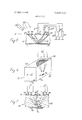
- FIG. 6 shows a zone plate optics 59, and a gold Schottky barrier contact 65 located at two different surfaces 69 and 70 of a semiconducting block 71 of N-type silicon. 59 focuses incident light beams 77 onto 65. Contacts to photocell 65 are 75 and 76.
- the ovonic switch 80 integrated structurally and electrically with a zone plate optics 16 as shown in FIG. 7.
- the ovonic switch 80 comprises an amorphous semiconducting body 81 of a glass containing 10% Ge, 12% Si, 48% Te and 30% As.
- the current voltage characteristics of this material between two metallic Ni contacts 82 and 83 can be of a comparatively high resistance, or else low resistance, depending on the magnitude of the applied voltage between these contacts and on the previous electrical history. Reversible, or else permanent switching from one state to the other is possible.
- the permanent switch arises by formation of a conducting channel 84 representing a compositionally and crystallographically different state of the material.
- This channel grows from the anode 82 when applying a suitable field.
- growth of the channel can be assisted by illumination 22 focused at the anode 82 by 16. This provides an optical means for selection of the spot 87 at which the channel 84 terminates at the electrode 82.
- the permanently conducting state can be erased, and the insulating state introduced, by applying a high current pulse with a sharp trailing edge. I have found that this erasing can be achieved also, or at least assisted, by a properly focused light pulse of high intensity.
- the focusing of light beam 22 occurs by the zone plate 16, whose central region 83 serves as contact to the ovonic switch.
- the zones 85, 86 and 88 are dimensioned to focus incident coherent monochromatic light 22 on a position 87 of electrode 82.
- An integrated electrooptical structure comprising a semiconducting body, a photoelectric device active for radiation to which said body is substantially transparent, and a diffractive image-forming means, both located at the same first surface of said body and arranged to focus said radiation with respect to said device after reflection at a second surface of said body opposite to said first surface.
- said photoelectric device is a photocell and comprises a Schottky barrier contact.
- said photoelectric device is a Schottky barrier contact to the base layer of a bipolar transistor and said electric component is said bipolar transistor amplifying the photocurrent of said Schottky barrier contact.
- said photoelectric device is a disk-shaped Schottky barrier contact to a semiconducting body, said disk-shaped contact being the central region of said zone plate, said other portion being an opaque region of said zone plate, and also the gate electrode of a field effect transistor, said field effect transistor electrically connected to amplify the photocurrent of said photoelectric device.
- a semiconducting body a plurality of photoelectric devices on a surface of said body, said photoelectric devices active to radiation to which said body is substantially transparent, a diffractive image-forming means on said body arranged to focus a plurality of beams of said radiation with respect to said plurality of photoelectric devices.
- portions of said image-fonning means are electric elements of said plurality of photoelectric devices and said focused radiation passing between said image-forming means and said plurality of devices is reflected at the opposite surface of said body.
- said photoelectric devices are Schottky barrier photocells
- said image-forming means is a zone plate, comprising conducting opaque regions as Schottky barrier contacts to said photocells.
- a semiconducting body a photoelectric device active for radiation to which said semiconducting body is substantially transparent and located at a first surface of said body, an image-forming means located at a second surface of said body,
- An ovonic switch integrated with a zone plate into a monolithic solid structure whereby part of said zone plate is a contact to said ovonic switch.
Abstract
Integrated electro-optical structures are disclosed which comprise a diffractive image-forming means on a transparent semiconductive body in optical alignment with a photoelectric element on said body. In particular, image-forming means and photoelectrical element are located at the same surface of said body and radiation passes between them by reflection on the opposite surface of the body. This arrangement permits extensive electric integration of conducting portions of image-forming means with a photoelectric device.
Description
United States Patent [15] 3,649,837 Lehovec Mar. M, 1972 [54] DIFFRACTIVE IMAGE-FORMING [56] References Cited MEANS INTEGRATED INTO OTHER PUBLICATIONS SEMICONDUCTING DEVICES Inventor: Kurt Lehovec, l1 Woodlawn Drive, Williamstown, Mass. 01267 Filed: Apr. 27, 1970 Appl. No.: 32,160
Related U.S. Application Data Continuation-in-part of Ser. No. 653,245, July 13, 1967, Pat. No. 3,569,997.
U.S. Cl .250/2111, 250/217 SS, 313/108 D,
317/235 N, 350/162 ZP Int. Cl. ..G02b 5/18, HOlj 39/12, H011 11/00 Field otSearch .317/235 UA,235 N; 350/162 2?;
250/217 SS, 83.31R, 211 J, 214; 313/110, 108 D Schottky barrier devices show current increase under pressure," Electronics, Sept. 15, l969,pp. 223 224 Baertsch et al., An Ag-GaAs Schottky-Barrier Ultraviolet Detector, Journal of Applied Physics, Vol. 40, N0. 1, Jan. 1969. Pp 229- 235 Primary Examiner-James W. Lawrence Assistant Examiner-T. N. Grigsby [57] ABSTRACT Integrated electro-optical structures are disclosed which comprise a difiractive image-forming means on a transparent semiconductive body in optical alignment with a photoelectric element on said body. In particular, image-forming means and photoelectrical element are located at the same surface of said body and radiation passes between them by reflection on the opposite surface of the body. This arrangement permits extensive electric integration of conducting portions of image-forming means with a photoelectric device.
16 Claims, 7 Drawing Figures IIIIIIIIIIIIIIIIIIIIIIllllllllllll DIFFRACTIVE IMAGE-FORMING MEANS INTEGRATED INTO SEMICONDUCTING DEVICES CROSS-REFERENCE TO RELATED APPLICATION This application is a continuation-in-part of U.S. application Ser. No. 653,245, now U.S. Pat. No. 3,569,997, filed on July 13, 1967.
BACKGROUND OF THE INVENTION Application Ser. No. 653,245, now U.S. Pat. No. 3,569,997, teaches the intimate inseparable combination of zone plate optics with semiconductive photoelectric devices into monolithic solid-state structures. Application Ser. No. 653,245 also teaches the use of a portion of the zone plate as part of an electrical structure in addition to its use as an optical component.
There is a large variety of structures within the broad scope of the inventive concept of Ser. No. 653,245 due to the many types of photoelectric semiconductive devices, and due to the many ways in which a conducting segment of a zone plate can be used as portion of electrical components.
It is a first object of the present invention to describe integrated monolithic solid combinations of zone plates with photoelectric devices which offer new and unexpected advantages with respect to simplicity of structure and usefulness.
It is another object of this invention to describe integrated combinations of a photocell, an amplifying element for the photoelectric current of said photocell and a zone plate optics.
It is yet another object of this invention to describe integrated combination of a zone plate optics with a plurality of photocells.
It is still another object of this invention to describe the integration of a zone plate optics with an ovonic switch thereby causing optically controlled switching action of improved reliability.
These and other objectives of my invention will be described in what follows.
BRIEF SUMMARY OF THE INVENTION This invention concerns the integration of certain devices of the broad class of photoelectric devices as defined in my application Ser. No. 653,245, now U.S. Pat. No. 3,569,997, with a diffractive image-forming means, whereby both photoelectric device and imageforming means are located at a surface of a transparent semiconducting body. This body has the dual function of optical spacing of photoelectric device from image-forming means and of electric element for the semiconducting device.
The photoelectric devices of this invention are photocells and/or light emitters. Because of the well-known reversibility of direction of radiation with respect to image-forming means, for each inventive arrangement of a photocell with respect to a diffractive optical means there exists a corresponding arrangement involving a light emitter replacing the photocell.
In order that the semiconducting body is transparent to the radiation in question, the photoelectric devices must be active with respect to radiation of a wavelength which is longer than that corresponding to the absorption edge of the semiconducting body. This is achieved by using Schottky barrier diodes as photocells and heterojunctions between the semiconducting body and another semiconductor of smaller band gap as light emitters and/or photocells.
While the diffractive image-forming means can be located (i) at the same surface of the transparent body as the photoelectric device, or else (ii) at the opposite surface; as illustrated in FIG. 9 of my application Ser. No. 653,245, now U.S. Patent No. 3,569,997, or else (iii) at a surface substantially at right angles from the photoelectric device, the location at the same surface offers particular advantages for planar technology processing, for precise alignment between imageforrning means and photoelectric device, and for electric integration of portions of the zone plate with the photoelectric device or associated circuitry. In this preferred case, the back surface is utilized as a mirror for radiation passing from imageforming means to photoelectric device.
Highly integrated structures are made by using conducting segments of the zone plate as electrical contacts to photocell and to an associated amplifier, or by using these segments as contacts to a multiplicity of photocells enabling sensing of the off-axis position of an object.
By focusing radiation by means of a zone plate integrated with an ovonic switch on a point of the electrode of this switch, its switching action can be affected optically.
BRIEF DESCRIPTION OF DRAWINGS FIG. 1 shows a heterojunction light emitter integrated with a zone plate optics located at the same surface of a transparent body.
FIG. 2 shows a Schottky barrier photocell integrated with a zone plate optics located at the same surface of a transparent semiconducting body.
FIG. 3 shows photocell and zone plate optics of FIG. 2 integrated electrically with a bipolar transistor amplifier for the photocell current.
FIG. 4 shows photocell and zone plate optics of FIG. 2 integrated electrically with an insulated gate field effect transistor.
FIG. 5 shows various sections of a zone plate optics used as Schottky barrier contacts for registration of angle of incidence of radiation with respect to the optical axis of the zone plate.
FIG. 6 shows a zone plate optics located at a first surface of a transparent semiconducting body and focusing radiation on a Schottky barrier photocell located at another surface of said body.
FIG. 7 shows an ovonic switch integrated with a zone plate optics according to this invention.
SPECIAL EMBODIMENTS Preferred photoelectric devices of this invention are Schottky barrier contacts and PN heterojunctions. A Schottky barrier contact is a metal contact to a semiconductor causing a depletion region of majority carriers in the adjacent semiconductor. Schottky barriers arise by suitable choice of the metal (in particular, its work function) in combination with a suitable semiconducting material containing appropriate dopant impurities. For instance, in the case of a gold electrode to N- type silicon of about l0' /cc. dopant concentration, electrons leaving the gold and entering the conduction band of silicon have to overcome an energy step of 0.8 electron volt, while electrons leaving the valence band and entering the gold have to acquire an energy of 0.3 electron volt. Gold forms a Schottky barrier with P-type silicon if the dopant concentration is sufficiently large that the Fermi level in the bulk of the silicon is above the valence band by less than 0.3 electron volt.
Another well-known means of producing a Schottky barrier to silicon consists of platinum heated in contact with silicon to about 550 C. to produce platinum silicide.
Aluminum to N-type GaAs forms a Schottky barrier contact of about 0.8 electron volt barrier height.
The electron flow from a negatively biased Schottky barrier contact into the semiconductor is limited by emission rate of electrons from the metal over the barrier. The emission current is enhanced greatly by illumination of the metal with light of a sufficiently short wavelength that its photon energy is larger than the barrier height. Thus, a Schottky barrier acts as a photocell. In the preferred embodiment for this invention, the metal is illuminated through the semiconducting body.
l-leterojunctions are boundaries between two semiconducting materials of somewhat different band gap. Well-known examples are mixed crystals of Ge-Si, or else GaAs-Ga? differing in the concentration of the constituents at either side of the junction. Light emitted from the shorter band gap material of a forward biased PN heterojunction penetrates readily the wider band gap material, e.g., GaAs-light emission penetrates Gal.
Diffraction optical means comprise a suitable arrangement of regions difi'racting incident radiation. In a circular zone plate, these regions may be opaque metallized ring-shaped zones separated by adjacent transparent rings. The opaque rings can be replaced by rings of a transparent material and of suitable thickness and refractive index to provide a phase shift 1r, i.e., optical path difference of M2, as compared with said adjacent rings. The phase shift can be caused by depositing a transparent material at certain positions, or else by shaping the surface profile of the semiconducting body. In general, many such zones are used, but only a few will be shown in the illustrations for sake of simplifying the drawings. Furthermore, dimensions are not drawn to scale for sake of clarity of representation.
The height of the transparent rings providing a phase shift of 1r, and the thickness of the opaque metal rings are of the order of 0.1 to 1 micron. The thickness of a transparent semiconducting wafer is typically of the order of 200 microns. For plane wave incident light to be focused on a surface photoelectric element, such as shown in FIGS. 1-5, using reflection at the back surface, the focal length becomes thus 400 microns. Considering the vacuum wavelength of light of about 1 micron, the refractive index of the semiconductor of 3-4, and the focal length of 400 microns, it is found that ring spacing of the zone plate becomes of the order of 20 microns.
This is a very convenient order of magnitude for standard semiconductor photolithography processing. By contrast, spacing the zone plate from underlying semiconductor surface by a transparent insulating layer of only I micron thickness, would require comparatively small ring distances, if the zone plate were designed to focus on a photoelectric element located at said surface of the semiconducting body.
Referring now to FIG. 1, there is shown in cross section a semiconducting body 1 of N-type GaAs -,P having on its upper surface 2 an overlayed P-type GaAs layer .3. Contact leads 4 and 5 connect to battery 6 and bias the PN heterojunction 12 between 3 and l in the forward direction. Light emitted from the heterojunction into the body 1 is reflected on the reflecting metal coating 7 located at the back surface 8 of 1 and is emitted through front surface 2, which has ringshaped grooves 9, 10, 11 appropriately chosen in location, width and depth to represent a zone plate optics 14 for the radiation emitted from 12, so that a plane parallel outgoing beam 13 is formed.
FIG. 2 shows a similar arrangement for a photocell exposed to incident coherent monochromatic radiation 22. N-type silicon body 21 shown in cross section carries the Schottky barrier contact 15 which represents also the central, opaque region of zone plate optics 16, located at top surface 17. Transparent SiO ring-shaped zones 18 and 19 are also parts of the zone plate, dimensional to focus 22 onto 15 after reflection at the lower surface 23. Opaque metallized zone serves as ohmic contact to underlying heavily doped n region 29 as well as a part of 16. The lower surface 23 of 21 is coated by a reflective SiO coating 24 dimensioned to reflect selectively the wavelength of 22. Contact leads 25 and 26 bias the Schottky barrier contact between 15 and 21 in the blocking direction by means of battery 27. Illumination of 15 causes a photocurrent through load 28 in response to 22. Note that Schottky barrier is shielded by 15 against incident undiffracted light. Rims of Schottky barrier can be shielded also by an overlay arrangement such as shown in FIG. 4.
F IG. 2 shows some electrical integration of zone plate optics in that contacts 15 and 20 are used as part of zone plate 16.
Further electrooptical integration is shown in FIG. 3 where opaque central zone 15 of zone plate 16 is the Schottky barrier contact to base region 30 of a PNP-transistor 36. Opaque zone 98 is a metal emitter contact to a ring-shaped p region 31 and opaque metal zone 20 is the ohmic contact to the p zone 32 of collector region 33. Opaque zone 99 is used only as an optical element of 16. Battery 34 provides the forward bias of emitter vs. collector and battery 35 provides the blocking bias of 15 against 30. Illumination of 15 causes flow of base current which is amplified in PNP-transistor 36 and flows through load resistance 37. Incident light 22 is diffracted onto 15 after reflection on grounded metallized base contact 7 in the same manner as shown in FIG. 2.
FIG. 4 shows another integrated structure of Schottky barrier photocell 15 which is central portion of zone plate optics 16. Output of 15 is amplified by insulated gate field effect transistor 40 located on ring-shaped p-silicon island 41 in nsilicon body 42. Opaque ring-shaped metal regions 98, 99 and 20 of zone plate optics 16 are spaced from silicon substrate by transparent insulating SiO, film 43 which has openings for contact access of 15, 98 and 20 to silicon. 98 and 20 are contacts to n source and drain regions 44 and 45 of 40. 99 is insulated gate contact. Illumination of 15 by light focused by 16 on 15 after reflection 0n 7 stimulates electron flow from negatively biased 15 into grounded 42. This generates a potential across the large resistance 46 and thus provides a positive bias to gate 99 vs. p-substrate 41, thereby generating an n-channel current between 44 and 45, which provides amplified current through output load 47 in series with drain battery 48.
Use of a zone plate offers two advantages compared with a directly illuminated Schottky barrier without zone plate optics. First, the amount of radiation impinging on the Schottky contact is increased, enabling the selection of smaller contacts with accordingly lower emission current in the dark. Secondly, the opaque central portion of the zone plate shields the Schottky contact from direct broad spectrum illumination, thus reducing noise signals due to undesired background radiation.
FIG. 5 shows in cross section a structure similar to that of FIG. 2, except that regions 15, 98 and 20 of the zone plate 16 are now metallized Schottky barrier photocells, each con nected to its own output circuit, as indicated by batteries and load resistances 27, 28; 27', 28'; 27", 28". Vertically incident beams 22 are focused on photocell 15 as was indicated in FIG. 2. Slanted incident beams 22" are focused on 98, and even more slanted beams 22" focused on 20. Thus, the arrangement of FIG. 5 permits registration of polar angle of incidence of beam with respect to optical axis of zone plate. A circular zone, such as 20, can be interrupted along certain radii and thus composed of individual sections isolated from each other thereby providing also registration of longitudinal angles of incident beams around optical axis of 16.
The zone plate optics of FIGS. 1-5 is located at the same surface of the transparent semiconducting body as the electrooptical element. FIG. 6 shows a zone plate optics 59, and a gold Schottky barrier contact 65 located at two different surfaces 69 and 70 of a semiconducting block 71 of N-type silicon. 59 focuses incident light beams 77 onto 65. Contacts to photocell 65 are 75 and 76.
Another integrated electrooptical structure according to this invention is the ovonic switch 80 integrated structurally and electrically with a zone plate optics 16 as shown in FIG. 7. The ovonic switch 80 comprises an amorphous semiconducting body 81 of a glass containing 10% Ge, 12% Si, 48% Te and 30% As. The current voltage characteristics of this material between two metallic Ni contacts 82 and 83 can be of a comparatively high resistance, or else low resistance, depending on the magnitude of the applied voltage between these contacts and on the previous electrical history. Reversible, or else permanent switching from one state to the other is possible.
It is known that the permanent switch (also called memory switch) arises by formation of a conducting channel 84 representing a compositionally and crystallographically different state of the material. This channel grows from the anode 82 when applying a suitable field. According to my invention, growth of the channel can be assisted by illumination 22 focused at the anode 82 by 16. This provides an optical means for selection of the spot 87 at which the channel 84 terminates at the electrode 82. It is known that the permanently conducting state can be erased, and the insulating state introduced, by applying a high current pulse with a sharp trailing edge. I have found that this erasing can be achieved also, or at least assisted, by a properly focused light pulse of high intensity. In FIG. 7, the focusing of light beam 22 occurs by the zone plate 16, whose central region 83 serves as contact to the ovonic switch. The zones 85, 86 and 88 are dimensioned to focus incident coherent monochromatic light 22 on a position 87 of electrode 82.
The consequences of illumination on an ovonic device have been described here, using the so-called memory switch. lllumination affects also the so-called threshold switch where the conducting state changes reversibly into nonconducting state and vice versa at certain voltages. The magnitude of these voltages is affected by illumination with light concentrated on the conducting regions by a zone plate optics.
lclaim:
1. An integrated electrooptical structure comprising a semiconducting body, a photoelectric device active for radiation to which said body is substantially transparent, and a diffractive image-forming means, both located at the same first surface of said body and arranged to focus said radiation with respect to said device after reflection at a second surface of said body opposite to said first surface.
2. The structure of claim 1 whereby said second surface is coated with a reflective coating dimensioned to reflect selectively at the wavelength of said radiation.
3. The structure of claim 1 whereby said photoelectric device comprises a heterojunction between said semiconducting body and another semiconducting body of smaller band gap.
4. The structure of claim 1 whereby said photoelectric device is a light-emitting circuit element.
5. The structure of claim 1 whereby said photoelectric device is a photocell and comprises a Schottky barrier contact.
6. The structure of claim 1 whereby said diffractive imageforming means is a zone plate.
7. The structure of claim 6 whereby a portion of this Zone plate is conducting and is a contact to said photoelectric device.
8. The structure of claim 7 whereby another portion of said zone plate is also conducting and is a contact to an electric circuit component in said semiconducting body in circuit connection with said photoelectric device.
9. The structure of claim 8 whereby said photoelectric device is a Schottky barrier contact to the base layer of a bipolar transistor and said electric component is said bipolar transistor amplifying the photocurrent of said Schottky barrier contact.
10. The structure of claim 8 whereby said photoelectric device is a disk-shaped Schottky barrier contact to a semiconducting body, said disk-shaped contact being the central region of said zone plate, said other portion being an opaque region of said zone plate, and also the gate electrode of a field effect transistor, said field effect transistor electrically connected to amplify the photocurrent of said photoelectric device.
11. A semiconducting body, a plurality of photoelectric devices on a surface of said body, said photoelectric devices active to radiation to which said body is substantially transparent, a diffractive image-forming means on said body arranged to focus a plurality of beams of said radiation with respect to said plurality of photoelectric devices.
12. The structure of claim 11 whereby portions of said image-fonning means are electric elements of said plurality of photoelectric devices and said focused radiation passing between said image-forming means and said plurality of devices is reflected at the opposite surface of said body.
13. The structure of claim 11 whereby said photoelectric devices are Schottky barrier photocells, and said image-forming means is a zone plate, comprising conducting opaque regions as Schottky barrier contacts to said photocells.
14. A semiconducting body, a photoelectric device active for radiation to which said semiconducting body is substantially transparent and located at a first surface of said body, an image-forming means located at a second surface of said body,
and focusing said radiation with respect to said photoelectric device, said second surface being substantially orthogonal to said first surface.
15. An ovonic switch integrated with a zone plate into a monolithic solid structure whereby part of said zone plate is a contact to said ovonic switch.
16. The structure of claim 15 whereby said zone plate is designed to focus radiation on the channel of said ovonic switch thereby affecting its electrical characteristic.
Claims (16)
1. An integrated electrooptical structure comprising a semiconducting body, a photoelectric device active for radiation to which said body is substantially transparent, and a diffractive image-forming means, both located at the same first surface of said body and arranged to focus said radiation with respect to said device after reflection at a second surface of said body opposite to said first surface.
2. The structure of claim 1 whereby said second surface is coated with a reflective coating dimensioned to reflect selectively at the wavelength of said radiation.
3. The structure of claim 1 whereby said photoelectric device comprises a heterojunction between said semiconducting body and another semiconducting body of smaller band gap.
4. The structure of claim 1 whereby said photoelectric device is a light-emitting circuit element.
5. The structure of claim 1 whereby said photoelectric device is a photocell and comprises a Schottky barrier contact.
6. The structure of claim 1 whereby said diffractive image-forming means is a zone plate.
7. The structure of claim 6 whereby a portIon of this zone plate is conducting and is a contact to said photoelectric device.
8. The structure of claim 7 whereby another portion of said zone plate is also conducting and is a contact to an electric circuit component in said semiconducting body in circuit connection with said photoelectric device.
9. The structure of claim 8 whereby said photoelectric device is a Schottky barrier contact to the base layer of a bipolar transistor and said electric component is said bipolar transistor amplifying the photocurrent of said Schottky barrier contact.
10. The structure of claim 8 whereby said photoelectric device is a disk-shaped Schottky barrier contact to a semiconducting body, said disk-shaped contact being the central region of said zone plate, said other portion being an opaque region of said zone plate, and also the gate electrode of a field effect transistor, said field effect transistor electrically connected to amplify the photocurrent of said photoelectric device.
11. A semiconducting body, a plurality of photoelectric devices on a surface of said body, said photoelectric devices active to radiation to which said body is substantially transparent, a diffractive image-forming means on said body arranged to focus a plurality of beams of said radiation with respect to said plurality of photoelectric devices.
12. The structure of claim 11 whereby portions of said image-forming means are electric elements of said plurality of photoelectric devices and said focused radiation passing between said image-forming means and said plurality of devices is reflected at the opposite surface of said body.
13. The structure of claim 11 whereby said photoelectric devices are Schottky barrier photocells, and said image-forming means is a zone plate, comprising conducting opaque regions as Schottky barrier contacts to said photocells.
14. A semiconducting body, a photoelectric device active for radiation to which said semiconducting body is substantially transparent and located at a first surface of said body, an image-forming means located at a second surface of said body, and focusing said radiation with respect to said photoelectric device, said second surface being substantially orthogonal to said first surface.
15. An ovonic switch integrated with a zone plate into a monolithic solid structure whereby part of said zone plate is a contact to said ovonic switch.
16. The structure of claim 15 whereby said zone plate is designed to focus radiation on the channel of said ovonic switch thereby affecting its electrical characteristic.
Applications Claiming Priority (2)
| Application Number | Priority Date | Filing Date | Title |
|---|---|---|---|
| US65324567A | 1967-07-13 | 1967-07-13 | |
| US3216070A | 1970-04-27 | 1970-04-27 |
Publications (1)
| Publication Number | Publication Date |
|---|---|
| US3649837A true US3649837A (en) | 1972-03-14 |
Family
ID=26708057
Family Applications (1)
| Application Number | Title | Priority Date | Filing Date |
|---|---|---|---|
| US32160A Expired - Lifetime US3649837A (en) | 1967-07-13 | 1970-04-27 | Diffractive image-forming means integrated into semiconducting devices |
Country Status (1)
| Country | Link |
|---|---|
| US (1) | US3649837A (en) |
Cited By (12)
| Publication number | Priority date | Publication date | Assignee | Title |
|---|---|---|---|---|
| US4225380A (en) * | 1978-09-05 | 1980-09-30 | Wickens Justin H | Method of producing light emitting semiconductor display |
| DE3140217A1 (en) * | 1980-10-09 | 1982-05-27 | Canon K.K., Tokyo | "READER" |
| US4378255A (en) * | 1981-05-06 | 1983-03-29 | University Of Illinois Foundation | Method for producing integrated semiconductor light emitter |
| US4809076A (en) * | 1986-04-16 | 1989-02-28 | Hitachi, Ltd. | Imaging apparatus using solid state image sensor |
| US5038354A (en) * | 1985-07-16 | 1991-08-06 | Mitsubishi Denki Kabushiki Kaisha | Semiconductor light emitting, light concentrating device |
| US5074646A (en) * | 1989-04-28 | 1991-12-24 | At&T Bell Laboratories | Planar reflective optical devices |
| US5078514A (en) * | 1990-03-27 | 1992-01-07 | Commissariat A L'energie Atomique | Switch and system for switching integrated optical multichannels and switch production method |
| US5181220A (en) * | 1985-07-16 | 1993-01-19 | Mitsubishi Denki Kabushiki Kaisha | Semiconductor light emitting light concentration device |
| US6804013B2 (en) * | 2000-01-26 | 2004-10-12 | Krypton Electronic Engineering N.V. | Optical element |
| US20090231677A1 (en) * | 2008-03-13 | 2009-09-17 | Usa As Represented By The Administrator Of The National Aeronautics And Space Administration | Variable Focal Point Optical Assembly Using Zone Plate and Electro-Optic Material |
| US20100039644A1 (en) * | 2008-08-15 | 2010-02-18 | United States Of America As Represented By The Administrator Of The National Aeronautics And Spac | Arrayed Micro-Ring Spectrometer System and Method of Use |
| US20100118683A1 (en) * | 2008-08-15 | 2010-05-13 | Administrator Of The National Aeronautics | Devices And Methods For A Micro-Fresnel Zone Plate Optical Device |
-
1970
- 1970-04-27 US US32160A patent/US3649837A/en not_active Expired - Lifetime
Non-Patent Citations (2)
| Title |
|---|
| Baertsch et al., An Ag GaAs Schottky Barrier Ultraviolet Detector, Journal of Applied Physics, Vol. 40, N0. 1, Jan. 1969, pp. 229 235 * |
| Schottky barrier devices show current increase under pressure, Electronics, Sept. 15, 1969, pp. 223 224 * |
Cited By (15)
| Publication number | Priority date | Publication date | Assignee | Title |
|---|---|---|---|---|
| US4225380A (en) * | 1978-09-05 | 1980-09-30 | Wickens Justin H | Method of producing light emitting semiconductor display |
| DE3140217A1 (en) * | 1980-10-09 | 1982-05-27 | Canon K.K., Tokyo | "READER" |
| US4539482A (en) * | 1980-10-09 | 1985-09-03 | Canon Kabushiki Kaisha | Reading apparatus |
| US4378255A (en) * | 1981-05-06 | 1983-03-29 | University Of Illinois Foundation | Method for producing integrated semiconductor light emitter |
| US5181220A (en) * | 1985-07-16 | 1993-01-19 | Mitsubishi Denki Kabushiki Kaisha | Semiconductor light emitting light concentration device |
| US5038354A (en) * | 1985-07-16 | 1991-08-06 | Mitsubishi Denki Kabushiki Kaisha | Semiconductor light emitting, light concentrating device |
| US4809076A (en) * | 1986-04-16 | 1989-02-28 | Hitachi, Ltd. | Imaging apparatus using solid state image sensor |
| US5074646A (en) * | 1989-04-28 | 1991-12-24 | At&T Bell Laboratories | Planar reflective optical devices |
| US5078514A (en) * | 1990-03-27 | 1992-01-07 | Commissariat A L'energie Atomique | Switch and system for switching integrated optical multichannels and switch production method |
| US6804013B2 (en) * | 2000-01-26 | 2004-10-12 | Krypton Electronic Engineering N.V. | Optical element |
| US20090231677A1 (en) * | 2008-03-13 | 2009-09-17 | Usa As Represented By The Administrator Of The National Aeronautics And Space Administration | Variable Focal Point Optical Assembly Using Zone Plate and Electro-Optic Material |
| US20100039644A1 (en) * | 2008-08-15 | 2010-02-18 | United States Of America As Represented By The Administrator Of The National Aeronautics And Spac | Arrayed Micro-Ring Spectrometer System and Method of Use |
| US20100118683A1 (en) * | 2008-08-15 | 2010-05-13 | Administrator Of The National Aeronautics | Devices And Methods For A Micro-Fresnel Zone Plate Optical Device |
| US8018815B2 (en) | 2008-08-15 | 2011-09-13 | The United States Of America As Represented By The Administrator Of The National Aeronautics And Space Administration | Micro-Fresnel zone plate optical devices using densely accumulated ray points |
| US8174695B2 (en) | 2008-08-15 | 2012-05-08 | The United States Of America As Represented By The Administrator Of The National Aeronautics And Space Administration | Arrayed micro-ring spectrometer system and method of use |
Similar Documents
| Publication | Publication Date | Title |
|---|---|---|
| US3950738A (en) | Semi-conductor non-volatile optical memory device | |
| US3569997A (en) | Photoelectric microcircuit components monolythically integrated with zone plate optics | |
| US3649837A (en) | Diffractive image-forming means integrated into semiconducting devices | |
| US4242695A (en) | Low dark current photo-semiconductor device | |
| US4427990A (en) | Semiconductor photo-electric converter with insulated gate over p-n charge storage region | |
| US4791468A (en) | Radiation-sensitive semiconductor device | |
| US4212019A (en) | Avalanche photodiode | |
| JPS6149822B2 (en) | ||
| US4965212A (en) | Optical sensor | |
| US3763372A (en) | Zone plate optics monolithically integrated with photoelectric elements | |
| US3704376A (en) | Photo-electric junction field-effect sensors | |
| US3473032A (en) | Photoelectric surface induced p-n junction device | |
| US4278986A (en) | Semiconductor diode | |
| US3324297A (en) | Radiation-sensitive semi-conductor device having a substantially linear current-voltage characteristic | |
| US3453507A (en) | Photo-detector | |
| US3631360A (en) | Electro-optical structures utilizing fresnel optical systems | |
| JPS61129883A (en) | Photodetector | |
| US4057819A (en) | Semiconductor device | |
| US3840741A (en) | Semiconductor delay line detector for equalization of optical fiber dispersion | |
| US5532999A (en) | Optical detector having stray carrier absorption regions between light receiving elements, and an optical head using the same | |
| US4488038A (en) | Phototransistor for long wavelength radiation | |
| US3452206A (en) | Photo-diode and transistor semiconductor radiation detector with the photodiode biased slightly below its breakdown voltage | |
| GB1458076A (en) | Optical memory devices and memory systems | |
| US6734515B1 (en) | Semiconductor light receiving element | |
| US4608587A (en) | Semiconductor optoelectro transducer |