US3772612A - Light modulator - Google Patents
Light modulator Download PDFInfo
- Publication number
- US3772612A US3772612A US00143089A US3772612DA US3772612A US 3772612 A US3772612 A US 3772612A US 00143089 A US00143089 A US 00143089A US 3772612D A US3772612D A US 3772612DA US 3772612 A US3772612 A US 3772612A
- Authority
- US
- United States
- Prior art keywords
- light
- insulator
- insulating layer
- layer
- cathode
- Prior art date
- Legal status (The legal status is an assumption and is not a legal conclusion. Google has not performed a legal analysis and makes no representation as to the accuracy of the status listed.)
- Expired - Lifetime
Links
- 229910052751 metal Inorganic materials 0.000 claims abstract description 25
- 239000002184 metal Substances 0.000 claims abstract description 25
- 239000012212 insulator Substances 0.000 claims description 53
- 230000001939 inductive effect Effects 0.000 claims description 3
- 229910021645 metal ion Inorganic materials 0.000 claims description 3
- 150000002739 metals Chemical class 0.000 claims description 3
- 230000003647 oxidation Effects 0.000 claims description 3
- 238000007254 oxidation reaction Methods 0.000 claims description 3
- 239000004793 Polystyrene Substances 0.000 abstract description 32
- 229920002223 polystyrene Polymers 0.000 abstract description 32
- 229910052737 gold Inorganic materials 0.000 abstract description 25
- 239000010931 gold Substances 0.000 abstract description 25
- 229910052782 aluminium Inorganic materials 0.000 abstract description 23
- XAGFODPZIPBFFR-UHFFFAOYSA-N aluminium Chemical compound [Al] XAGFODPZIPBFFR-UHFFFAOYSA-N 0.000 abstract description 23
- PCHJSUWPFVWCPO-UHFFFAOYSA-N gold Chemical compound [Au] PCHJSUWPFVWCPO-UHFFFAOYSA-N 0.000 abstract description 18
- -1 gold ions Chemical class 0.000 abstract description 7
- 230000004044 response Effects 0.000 abstract description 7
- 239000000463 material Substances 0.000 abstract description 5
- 150000002500 ions Chemical class 0.000 description 10
- 230000000694 effects Effects 0.000 description 8
- 230000005684 electric field Effects 0.000 description 8
- 230000001965 increasing effect Effects 0.000 description 6
- 238000000034 method Methods 0.000 description 6
- 238000010521 absorption reaction Methods 0.000 description 5
- 230000008021 deposition Effects 0.000 description 5
- 230000008569 process Effects 0.000 description 5
- 230000002238 attenuated effect Effects 0.000 description 4
- 239000011521 glass Substances 0.000 description 4
- 230000031700 light absorption Effects 0.000 description 4
- 238000004519 manufacturing process Methods 0.000 description 4
- 230000003287 optical effect Effects 0.000 description 4
- 230000001443 photoexcitation Effects 0.000 description 4
- QVGXLLKOCUKJST-UHFFFAOYSA-N atomic oxygen Chemical compound [O] QVGXLLKOCUKJST-UHFFFAOYSA-N 0.000 description 3
- 230000003247 decreasing effect Effects 0.000 description 3
- 238000002347 injection Methods 0.000 description 3
- 239000007924 injection Substances 0.000 description 3
- 230000007246 mechanism Effects 0.000 description 3
- 239000001301 oxygen Substances 0.000 description 3
- 229910052760 oxygen Inorganic materials 0.000 description 3
- 238000003860 storage Methods 0.000 description 3
- 239000000758 substrate Substances 0.000 description 3
- IJGRMHOSHXDMSA-UHFFFAOYSA-N Atomic nitrogen Chemical compound N#N IJGRMHOSHXDMSA-UHFFFAOYSA-N 0.000 description 2
- 238000004458 analytical method Methods 0.000 description 2
- 230000004888 barrier function Effects 0.000 description 2
- 230000005540 biological transmission Effects 0.000 description 2
- 230000001427 coherent effect Effects 0.000 description 2
- 230000001419 dependent effect Effects 0.000 description 2
- 238000009792 diffusion process Methods 0.000 description 2
- 230000005284 excitation Effects 0.000 description 2
- 150000001455 metallic ions Chemical group 0.000 description 2
- 238000005036 potential barrier Methods 0.000 description 2
- 230000000717 retained effect Effects 0.000 description 2
- 238000000926 separation method Methods 0.000 description 2
- 230000007847 structural defect Effects 0.000 description 2
- 241001501930 Gavia Species 0.000 description 1
- 239000006096 absorbing agent Substances 0.000 description 1
- 230000002411 adverse Effects 0.000 description 1
- 238000007743 anodising Methods 0.000 description 1
- 230000006399 behavior Effects 0.000 description 1
- 238000005452 bending Methods 0.000 description 1
- 238000005513 bias potential Methods 0.000 description 1
- 230000000740 bleeding effect Effects 0.000 description 1
- 230000008859 change Effects 0.000 description 1
- 239000004020 conductor Substances 0.000 description 1
- 238000004132 cross linking Methods 0.000 description 1
- 230000007547 defect Effects 0.000 description 1
- 238000009826 distribution Methods 0.000 description 1
- 230000009881 electrostatic interaction Effects 0.000 description 1
- 230000001747 exhibiting effect Effects 0.000 description 1
- 230000006870 function Effects 0.000 description 1
- 239000001307 helium Substances 0.000 description 1
- 229910052734 helium Inorganic materials 0.000 description 1
- SWQJXJOGLNCZEY-UHFFFAOYSA-N helium atom Chemical compound [He] SWQJXJOGLNCZEY-UHFFFAOYSA-N 0.000 description 1
- 230000036039 immunity Effects 0.000 description 1
- 239000012535 impurity Substances 0.000 description 1
- 239000011261 inert gas Substances 0.000 description 1
- 238000009413 insulation Methods 0.000 description 1
- 230000014759 maintenance of location Effects 0.000 description 1
- 229910052757 nitrogen Inorganic materials 0.000 description 1
- 230000010355 oscillation Effects 0.000 description 1
- TWNQGVIAIRXVLR-UHFFFAOYSA-N oxo(oxoalumanyloxy)alumane Chemical compound O=[Al]O[Al]=O TWNQGVIAIRXVLR-UHFFFAOYSA-N 0.000 description 1
- 238000006116 polymerization reaction Methods 0.000 description 1
- 238000005381 potential energy Methods 0.000 description 1
- 230000001681 protective effect Effects 0.000 description 1
- 230000002829 reductive effect Effects 0.000 description 1
- 230000002441 reversible effect Effects 0.000 description 1
- 238000012216 screening Methods 0.000 description 1
- 239000006104 solid solution Substances 0.000 description 1
- 230000007704 transition Effects 0.000 description 1
- 239000012780 transparent material Substances 0.000 description 1
- 238000001429 visible spectrum Methods 0.000 description 1
- XLYOFNOQVPJJNP-UHFFFAOYSA-N water Chemical compound O XLYOFNOQVPJJNP-UHFFFAOYSA-N 0.000 description 1
Images


Classifications
-
- G—PHYSICS
- G02—OPTICS
- G02F—OPTICAL DEVICES OR ARRANGEMENTS FOR THE CONTROL OF LIGHT BY MODIFICATION OF THE OPTICAL PROPERTIES OF THE MEDIA OF THE ELEMENTS INVOLVED THEREIN; NON-LINEAR OPTICS; FREQUENCY-CHANGING OF LIGHT; OPTICAL LOGIC ELEMENTS; OPTICAL ANALOGUE/DIGITAL CONVERTERS
- G02F1/00—Devices or arrangements for the control of the intensity, colour, phase, polarisation or direction of light arriving from an independent light source, e.g. switching, gating or modulating; Non-linear optics
- G02F1/01—Devices or arrangements for the control of the intensity, colour, phase, polarisation or direction of light arriving from an independent light source, e.g. switching, gating or modulating; Non-linear optics for the control of the intensity, phase, polarisation or colour
- G02F1/17—Devices or arrangements for the control of the intensity, colour, phase, polarisation or direction of light arriving from an independent light source, e.g. switching, gating or modulating; Non-linear optics for the control of the intensity, phase, polarisation or colour based on variable-absorption elements not provided for in groups G02F1/015 - G02F1/169
Definitions
- ABSTRACT A metal-insulator-metal device formed of materials such as gold, polystyrene and aluminum.
- gold ions and electrons migrate from the gold and aluminum regions respectively and become trapped in the polystyrene.
- the device Upon removal of the voltage, the device acts as a light attenuator in a given light frequency range.
- the device may be switched to a second condition in which it is relatively transparent to light by applying thereto a relatively shorter duration, lower amplitude voltage pulse and also can be switched back to its light attenuating condition.
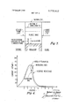
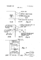
- FIGS. 1, 2, 3, 5, 6, 7, 8a, 8b, 9, 10a and 10b are energy state drawings to help explain the operation of the light modulator of the invention
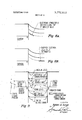
- FIG. 4 is a characteristic curve of current versus voltage for a device according to an embodiment of the invention.
- FIG. 1 l is a cross section through a device according to an embodiment of the invention.
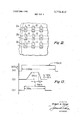
- FIG. 12 is a plan view of an embodiment of a page composer according to the invention.
- FIG. 13 is a drawing of waveforms employed in the operation of the embodiments illustrated in FIGS. 11 and 12.
- FIG. 11 illustrates the structure of a single device in accordance with an embodiment of the invention. It includes a very thin layer of aluminum which may be of the order of I Angstroms (A.) thick on a substrate formed of a transparent material such as glass. The aluminum is covered with a hard, amorphous spongelike insulator material such as polystyrene which may be of the order of 2,000 A. thick. A relatively thin layer of a second metal which has a considerably different oxidation potential than the first metal, is located on the polystyrene layer. A suitable metal has been found to be gold and the layer thickness also may be of the order of 100 A. Both metals are transparent at these thicknesses. A more detailed discussion of how the device may be fabricated is given later.
- a hard, amorphous spongelike insulator material such as polystyrene which may be of the order of 2,000 A. thick.
- a relatively thin layer of a second metal which has a considerably different oxidation potential than the first metal, is located on the poly
- a forward voltage (relatively positive at the gold anode and relatively negative at the aluminum cathode) such as one greater than about volts is applied between the gold and aluminum layers for a relatively long interval of time an interval of perhaps 5 to seconds.
- the apparatus for doing this may include a voltage source 14 and a switch 16 which is thrown to a position such that a relatively positive voltage appears at the gold electrode.
- a plasma is formed in the polystyrene layer and becomes trapped there.
- Photons incident on the device from light source 10 of FIG. 11 are believed also to photoexcite electrons from the induced band to the conduction band of the insulator.
- Two mechanisms are thought responsible for the electron population within the induced band.
- the first mechanism is electron photoexcitation from the valence band (mentioned above);
- the second mechanism is electron diffusion into the plasma from the Fermi level of the cathode via tunnelling between the adjacent metallic ions of the plasma. Electron diffusion is thought to be the major source of the space charge, and the amount of energy between the cathode Fermi level and the bottom of the conduction band is therefore a measure of the frequency of incident light, below which the attenuation will be substantially reduced.
- the shape of the pulse is not critical.
- the pulse duration r that is, the region of the pulse at about 8 volts amplitude, must be at least 10 nanoseconds, but may be greater.
- the trailing edge 1' must not exceed about 100ns, but may be shorter. Inpractice r,, so long as it is greater than l0ns is not critical and pulses as long as several hundred us may be used. Similarly, in practice, the pulse is turned off as quickly as possibly and so long as the turn-off time is less than lOOns, the dlesired operation is achieved.
- the leading edge shape and duration are not critical.
- the pulse amplitude should be substantially greater than 5 volts good results having been obtained with a pulse of about 8 volts amplitude.
- the device of FIG. 11 may be returned to the light absorbing condition by applying a forward pulse thereto such as shown in FIG. 130.
- This pulse is of relatively longer duration, say 200 nanoseconds or so, and of relatively lower amplitude, for example, 4 volts.
- the pulse amplitude should correspond approximately to the voltage at the current peak of the characteristic of FIG. 4, as discussed shortly.
- electrons flow relatively freely from the aluminum cathode through the polystyrene to the gold anode thereby removing the trapped space charge within the polystyrene.
- the device of FIG. 1 1 is found again to act as a light absorber.
- the fabrication of the device of FIG. 11 may be car ried out in the following way.
- the aluminum layer may be vacuum deposited on the glass through a mask. After deposition, the aluminum film is placed in an oxygen atmosphere of 10 torr for about 30 minutes to anodize the film (to cause a protective film of aluminum oxide to form over the surface of the aluminum).
- the purpose of anodizing is to provide some immunity to air borne impurities, water vapor, etc. when the sample later is removed from the vacuum system employed to lay down the metal to the vacuum system for the deposition of the polystyrene layer over the aluminum.
- polystyrene has been found to be a suitable material. The thickness mentioned previously is 2,000 A.; however, in practice thicknesses of between 1,000 to 3,000 A. have been found to provide satisfactory results.
- the polystyrene is layed down by bleeding polystyrene vapor into a vacuum system in which the aluminum on its substrate is located. During this deposition, a uniform electric field is continuously applied to the aluminum by a second circular electrode spaced over and about 1 inch from the aluminum surface.
- a voltage of several hundred volts may be employed to create a strong electric field normal to the aluminum surface. This voltage is left on during the entire deposition procedure which takes about 20 minutes.
- the continuous electric field present during the deposition causes polymerization and cross linking of the internal molecular structure of the polystyrene to occur. This geometrically complex insulator structurecaptures and stores the plasma, as discussed below.
- the device After the device has been fabricated in the manner discussed above, it is placed in a modest vacuum of about 1 micron and thereafter is maintained in this vacuum.
- the purpose of the vacuum is to remove absorbed and adsorbed oxygen from the device.
- the oxygen if present, adversely affects the device operation. It is believed to introduce surface states, to diffuse into the structural defects on the insulating film, and to establish internal screening potentials which impede anode ion injection into the polystyrene insulation layer.
- it is placed in a modest vacuum of about 1 micron and thereafter is maintained in this vacuum.
- the purpose of the vacuum is to remove absorbed and adsorbed oxygen from the device.
- the oxygen if present, adversely affects the device operation. It is believed to introduce surface states, to diffuse into the structural defects on the insulating film, and to establish internal screening potentials which impede anode ion injection into the polystyrene insulation layer.
- an inert gas environment such as one formed of nitrogen or helium.
- a forward bias potential (relatively positive at the gold anode and relatively negative at the aluminum cathode) of about volts is applied to the device for an interval of 5 to seconds to cause gold ions to be injected from the gold layer into the amorphous, sponge-type polystyrene insulator.
- the cathode injects an electron, thereby preserving charge neutrality within the polystyrene insulator.
- the anode ions which lie above the Fermi level of the insulator and the cathode electrons which lie below the Fermi level of the insulator together resemble a solid solution or congealed plasma with electrostatic interaction between its electrons and ions. Since the ions are randomly imbedded within the amorphous medium, there is no next neighbor or next nearest neighbor configuration. The ionic potential is therefore ill defined. Since the electrons occupy traps within the insulator whose distance to any one ion is random, the overall effect is a randomly perturbed, ill defined potential whichproduces otherwise excluded localized states within the forbidden energy gap of the insulator. This induced band is believed to be rather broad, of the order of one electron volt (ev) or more, and is believed to lie about 1.5 ev below the insulator conduction band and about 2.0 ev above the insulator valence band.
- ev electron volt
- FIG. 1 illustrates the insulator band structure prior to the time that the plasma described above has been injected into the insulator.
- FIG. 2 illustrates the band structure of the polystyrene after the plasma has been injected. For simplicity, interfacial band bending is not shown in these figures. I
- the 6,150 A. wavelength is believed to correspond to the energy difference between the top of the valence band and the bottom of the induced plasma band. At wavelengths longer than this, even with the plasma in the polystyrene as described above, insufficient photon energy exists optically to excite valence electrons into the induced band and no significant absorption of light takes place.
- the valence band optical excitation phenomenon is illustrated in FIG. 3.
- the plasma as discussed above can be removed from the polystyrene by applying a reverse bias voltage of say 5 to 1 0 volts for a relatively long interval of time say 5 to 10 seconds. This is accomplished in FIG. 11 by throwing the switch 16 to the proper position and placing the voltage source 14 at the proper level. If the sample is treated in this way, the induced band is removed and in the absence of this induced band, the incident photon energy (the incident light) is inadequate to excite valence electrons over the relatively large insulator energy gap into the conduction band (even at the lower optical wavelengths those well below 6,150 A.) and light absorption does not occur.
- the value of the peak current shown in FIG. 4 is of the order of milliamperes (ma.). This value can vary either way by as much as an order of magnitude, depending upon the thickness of the insulating layer, the magnitude of the ion injection, the quality of the vacuum environment, and other parameters.
- the magnitude of the voltage at which the peak current occurs has been found to be independent of the insulator thickness, thereby indicating that the effect illustrated in FIG. 4 is not electric field dependent. If the effect were field dependent, it would be expected that as the insulating layer thickness increased, the amount of voltage required to cause the device to exhibit a current peak would have to increase. Since the current 5 is peak is independent of layer thickness, it is clear that electric field is not involved. In this respect, the present device is believed to be completely different than all other known light modulators.
- the voltage at which peak current occurs is called the threshold voltage of the device and corresponds to the energy of the top of the induced band, referenced to the Fermi level in the insulating layer under zero bias, and in the absence of trapped charge. Since this threshold voltage is of the order of 4 volts and since half of the applied voltage is impressed across the cathode and interfacial depletion layers, the energy at the top of the induced band is believed to be of the order of 2 ev, as illustrated in FIG. 5. The power dissipation during current flow (FIG. 4) thus occurs across the electrodeinsulator depletion barriers.
- Quantitative analyses have been made of the polystyrene insulator after the gold ion electron plasma has been injected therein.
- the amount of gold physically present in the insulator has been found to be of the order of 10 atoms per cubic centimeter.
- Analyses of similar devices in which ions were not injected, showed insignificant numbers of anode atoms present in the insulator.
- the high anode atomic densities indicate the average ion separation to be about 25 A".
- the current density j clue to electrons from the cathode Fermi level can be shown to be given by:
- FIG. 6 illustrates the situation in which the external bias exceeds the threshold potential of the device.
- the first equation indicates an increase in current density j
- the presence of V in the exponential factor of the second equation indicates a decrease in current density j, with further increases in V. This model therefore predicts the negative resistance region of FIG. 4.
- the reason for the retention is that although the electrons are able to slide down the potential hill at the cathode-insulator interface, they are unable to climb the similar potential hill at the anode-insulator interface due to the absence of applied forward voltage. Since the density of states near the top of the induced band is low, tunnelling sites of equal energy are further apart. Therefore, sites which are close together have a high probability of differing in energy by more than kT (Boltzmanns constant and temperature absolute). The transport of trapped charge from the cathode toward the center of the insulator is therefore phonon-assisted since energy exchanges of the order of kT or more are involved. This is not true of the non-phonon assisted flow of transport current between adjacent ions where the density of states is high near the middle of the induced band.
- FIG. 7 shows the profile of the density of states versus energy and FIGS. 8A and 8B illustrate, respectively, the distribution of the trapped charge immediately upon the abrupt removal of the external bias (FIG. 8A), and a short time thereafter (FIG. 83).
- FIG. 88 Once having reached the center of the insulator, as shown in FIG. 88, each trapped electron oscillates between the two most probable localized states which it occupies, thereby avoiding transitions which involve higher energy exchange.
- the device therefore remembers the magnitude of the external bias above threshold just prior to its abrupt removal since the greater the voltage, the greater is the number of electrons (at energy V-,) trapped in the insulator.
- the effect of this stored charge is to reduce the internal electric field at the cathode-insulator interface, and therefore to increase the electrical impedance of the device.
- the energy of the bottom of the conduction band referred to the Fermi level at the cathode since the dominant attenuation appears to be electron photo excitation from the space charge within the induced band at the cathode Fermi level, this energy defines the absorption edge i.e., the minimum incident photon frequency, below which absorption into the conduction band cannot occur (in terms of light wavelength, it defines the maximum wavelength at which light absorption occurs).
- FIG. 9 illustrates the change in energy of the bottom of the conduction band, referred to the cathode, which occurs in response to the presence of trapped charge within the plasma.
- the upper levels are drawn continuous through the plasma, and correspond to the band structure for which charge is trapped 'within the plasma.
- the lower levels are drawn discontinuous, extending in toward the center of the insulator bed from either interface, and correspond to the band structure in the absence of trapped charge.
- the energy of the bottom of the conduction band referred to the Fermi level at the cathode. It is seen that this energy difference E increases with increasing magnitude of trapped charge.
- non-phonon assisted transport current that is, current flow which is substantially temperature independent
- non-phonon assisted transport current flows through the induced band from the cathode to the anode, exhibiting a current-voltage relationship of the kind illustrated in FIG. 4.
- the region labelled area differential in this figure increases with increasing rate of removal of the external bias, the magnitude of peak current for decreasing bias decreasing with more abrupt bias removal. This area between the two curves is a measure of the energy stored in the device, and increases with increasing magnitude of stored charge.
- the energy of the bottom of the conduction band E referred to the cathode Fermi level is increased. Since the space charge is in equilibrium with the cathode Fermi level, its energy is unchanged and the incident photon energy is insufficient to photo excite the space charge electrons into the conduction band. Thus, the incident photons are not attenuated and are transmitted through the device.
- the absorption process is illustrated in FIG. 10A in which stored charge is absent, and the transmission process is illustrated in FIG. 10B in which stored charge is present.
- a plurality of devices such as illustrated in FIG. 11 may be arranged in an array to form a so-called page composer for an optical'memory.
- the purpose of this composer is to translate a beam or several beams of light into an array of light and dark areas representing the binary digits 1 and 0 respectively.
- FIG. 12 Three-by-three locations of a page composer are illustrated in FIG. 12.
- the elements 20a, 20b and 200 are aluminum strips on a glass substrate. They are covered with an insulator such as polystyrene. At spaced regions over the aluminum layers are located an array of gold electrodes 51, 52, 61, 62 and so on. The thicknesses of the various layers are of the same order as those already discussed.
- the fabrication process is also similar to that discussed. After fabrication, the devices are placed in a suitable environment and a forward bias voltage is employed as already discussed for forming the plasma within the polystyrene insulator.
- the locations it is desired to act as transmitters are pulsed in the manner shown in FIG. 13b.
- the pulse of FIG. 13b is applied to the gold anodes at memory locations a a and c while all cathodes 20 are at ground, these locations are placed in the light transmitting state and all'other locations are in the light absorbing state.
- a beam of light may be passed through the page composer and focused onto a storage medium.
- the beam is a coherent light beam obtained from a laser.
- a second coherent light beam known as a reference beam is shined onto the same location of the storage medium at an angle with the so-called object beam from the page composer to form a hologram on the storage medium.
- This hologram may be developed and fixed and subsequently read out in conventional fashion. During readout, for example, the hologram images may be reconstructed over an array of light sensing devices for translating the optically stored bits to electrical signals.
- An important feature of the page composer of FIG. 12 is that its information content can be electronically changed.
- the old information can be erased by applying to each location a pulse such as shown in FIG. 130.
- This pulse causes the trapped charge to be swept toward the anode at each memory location and, for the reasons already discussed, when in this condition, each device contains no trapped charge and therefore attenuates light.
- the new information again may be written into the memory by selectively applying to certain of the locations the pulse shown in FIG. 13b to place these locations in their light transmitting condition.
- an insulating layer comprising polystyrene
- means for modulating said light comprising means for varying the amount of said charge
- a light detector for sensing the amount of light passing through said layer.
- means for inducing and trapping in said insulating layer having said plasma therein an electronically controllable charge comprising a metal layer on one surface of the insulating layer,
- said metal layer serving as a cathode
- means for modulating said light comprising means for varying the amount of said charge
- a light detector for sensing the amount of light passing through said layer.
- a light modulator comprising, in combination:
Abstract
A metal-insulator-metal device formed of materials such as gold, polystyrene and aluminum. In response to the application to the device of a forward voltage for a relatively long time interval, gold ions and electrons migrate from the gold and aluminum regions respectively and become trapped in the polystyrene. Upon removal of the voltage, the device acts as a light attenuator in a given light frequency range. The device may be switched to a second condition in which it is relatively transparent to light by applying thereto a relatively shorter duration, lower amplitude voltage pulse and also can be switched back to its light attenuating condition.
Description
[451 Nov. 13, 1973 4] LIGHT MODULATOR Robert Allen Gauge, Belle Mead, NJ.
[73] Assignee: RCA Corporation [22] Filed: May 13, 1971 [21] App]. No.: 143,089
[75] Inventor:
OTHER PUBLICATIONS Beam, Charge-Storage Beam Addressable Memory, 10/66, pg. 555-556, IBM Tech. Disc. Bu11., Vol. 9, No. 5.
Peters, I-F Modulator Using and Induced Conductor," 8/65, pg. 1148-1149, Proceedings of the IBBE Simmons, Effect of Deep Trgrs. MIM Tunnel Functions, 8/11/69, pg. 297-300, P.R.L., Vol. 23, No.
Simmons, Generalized Formula Thin Insulating Film, 6/63, pg. 1793-1803, J.A.P., Vol. 34, No. 6. Simmons et al., New Conduction in Thin 1. Films, 1967, Proceedings of the Royal Society, pg. 77-102, A-301.
Primary Examiner-Benjamin A. lBorchelt Assistant Examiner-N. Moskowitz Att0meyI-I. Christoffersen, Glenn H. Bruestle and Irwin M. Krittman [57] ABSTRACT A metal-insulator-metal device formed of materials such as gold, polystyrene and aluminum. In response to the application to the device of a forward voltage for a relatively long time interval, gold ions and electrons migrate from the gold and aluminum regions respectively and become trapped in the polystyrene. Upon removal of the voltage, the device acts as a light attenuator in a given light frequency range. The device may be switched to a second condition in which it is relatively transparent to light by applying thereto a relatively shorter duration, lower amplitude voltage pulse and also can be switched back to its light attenuating condition.
3 Claims, 15 Drawing Figures VOLTAGE SOURCE DETECTOR TOP OF 4 ANODE PAIENIEDNUY 13 I975 3772.612 sum 1 0F 6 VACUUM LEVEL BOTTOM OF CONDUCTION BAND ATH ANODE FEBQAQ FERMI LEVEL A ,rFORBIDDEN LEVEL ENERGY GAP I TOP OF VALANCE BAND QALADDB INSULATOR AN E vAcuuN "LEVEL BOTTOM OF CONDUCTION BAN INDUCED BAND FERMI LE EL 'B'DffDNDF" T INDUCED BAND ABOUT VREA NEE BAND Fry. 2.
CATHODE INSULATOR ANODE I N VEN TOR.
Robert A. Gangs ATTORNEY PAIENIEDnBv 3 0975 3,772.6 l 2 SHEET 20F 6 VACUUM LEVEL BOTTOM OF cowoucnow BAND CATHODE ANODE FERMI FERMI LEVEL LEVEL INDUCED BAND PHOTOEXCITATION FROM VALANCE-BAND- BMMGDOD T0 INDUCED BAND Fig. 3.
CATHODE INSULATOR ANODE |75-- AREA DIFFERENTIAL 3 [INCREASING B|As "g;
NEGATIVE RESISTANCE CURRENT B '3 A 5 B 7 8 5') |b INVENTOR.
0 b t 0 Fig. 4. BY A Gang? A TTORNE Y PAIENIEDNUV 13 I975 3.772.612
VACUUM LEVEL :BOTTOM OF CONDUCTION BAND LEVEL TERIII LEVEL wITHIN INSULATOR BED cATHDDE INSULATOR Fig. 5'.
INJECTED ELECTRON wITH ENERGY v-I TERIII LEVEL wITH Is TRAPPED ALONG TOP OF RIAs GREATER THAN INDucED BAND THRESHOLD I TERIIIIEvEIwITH E N I T BIAS EQUAL TO-- v THRESHOLD J.
1 WW ZERO TRANsPoRT CURRENT CATHODE INsIILAToR Fig 6.
/VACUUM LEVEL BOTTOM OF CONDUCTION BAND Fig; 7.
I N VEN TOR.
Robert A. Gang'e @ATNDEDEIAANIRA ATTORNEY PATENTEDIIDY T 3 I973 cATH'DDE III SHEET T BE 6 CATHODE 'ELECTRONS MOMENTARILY TRAPPED ALONG TOP OF INDUCED BAND TRAPPED ELECTRON EQUILIBRIUM DISTRIBUTION VACUUM LEVEL I I BOTTOM 0T" 7 CONDUCTION BAND TOPO BE' g gm {L DQE ND. APART li L v EL A 1". LEVEL STDBED' 5 -FERMILEhi CHARGE w--- B. ;fl INDUCED BAND STORED ABSENT "*{ZBOTTOMOF DT E uPPEBLEvT-1s= CHARGE INDUCED BAND l LOSJTEIAQRIDEEVEREBENT PRESENT Z OF :7 CHARGE ABSE VALANCE BAND VENTOR. Fig 9. BY chart .4. Gange 4 Q4! ATTORNEY PATENIEDNUV I 3 I975 3.772.512 SHEET 50F 6 VACUUM LEVEL INCIDENT PHOTON BOTTOM OF ENERGY=hv CONDUCTION BAND INDUCED 1' BAND x XOTTATTON F g 10.4 j 5* K-PLASMA FERMI LEVEL ZTRANSPORT SPACE CHARGE LEVEL INSULATOR :VACUUM LEVEL I BOTTOM OF f CONDUCTION BAND T TATION B E T O A LE EEXCI I 1:: Fig. 105. CITETFIgADE ZTRANSPORTSPACE CHARGE LEVEL INSULATOR LIGHT l0 SOURCE/1 i GOLD |00A POLYSTYRENE 2000A" ""g' 1 ALUMINUM IOOA |6 GLASS l INVENTOR. T i Robert A. Gange 5- 11 LIGHT DETECTOR ATTORNEY ucn'r MODULATOR SUMMARY OF THE INVENTION An induced energy band is created in the forbidden energy gap of an insulating layer by trapping in the layer a plasma consisting of positive metal ions and electrons. In this condition, the insulating layer attenuates light in a given frequency range. An electron space charge may be introduced and trapped in the insulating layer to switch it from its light attenuating to a light transmitting condition. The insulator may be switched back to its light attenuating condition by removing the electron space charge.
BRIEF DESCRIPTION OF THE DRAWING FIGS. 1, 2, 3, 5, 6, 7, 8a, 8b, 9, 10a and 10b are energy state drawings to help explain the operation of the light modulator of the invention;
FIG. 4 is a characteristic curve of current versus voltage for a device according to an embodiment of the invention;
FIG. 1 l is a cross section through a device according to an embodiment of the invention;
FIG. 12 is a plan view of an embodiment of a page composer according to the invention; and
FIG. 13 is a drawing of waveforms employed in the operation of the embodiments illustrated in FIGS. 11 and 12.
DETAILED DESCRIPTION FIG. 11 illustrates the structure of a single device in accordance with an embodiment of the invention. It includes a very thin layer of aluminum which may be of the order of I Angstroms (A.) thick on a substrate formed of a transparent material such as glass. The aluminum is covered with a hard, amorphous spongelike insulator material such as polystyrene which may be of the order of 2,000 A. thick. A relatively thin layer of a second metal which has a considerably different oxidation potential than the first metal, is located on the polystyrene layer. A suitable metal has been found to be gold and the layer thickness also may be of the order of 100 A. Both metals are transparent at these thicknesses. A more detailed discussion of how the device may be fabricated is given later.
After fabrication, a forward voltage (relatively positive at the gold anode and relatively negative at the aluminum cathode) such as one greater than about volts is applied between the gold and aluminum layers for a relatively long interval of time an interval of perhaps 5 to seconds. The apparatus for doing this may include a voltage source 14 and a switch 16 which is thrown to a position such that a relatively positive voltage appears at the gold electrode. In response to this forward voltage, it is thought that a plasma is formed in the polystyrene layer and becomes trapped there. It has been found that gold ions migrate from the gold anode and a corresponding number of electrons migrate from the cathode in response to the relatively positive voltage applied to the gold, and both the gold ions and the electrons become trapped in the polystyrene.
After the sample has been treated in this way, it is found that when light from source 10 is shined through the device to a light detector 12, a certain portion of this light, in'a given frequency range, is attenuated. In particular, light having a wavelength of 6,150 A. (corresponding to the color red in the visible spectrum) or less is attenuated by about percent. This attenuation is believed due to photoexcitation of electrons from the insulator valence band into the induced band of states.
Photons incident on the device from light source 10 of FIG. 11 are believed also to photoexcite electrons from the induced band to the conduction band of the insulator. Two mechanisms are thought responsible for the electron population within the induced band. The first mechanism is electron photoexcitation from the valence band (mentioned above); the second mechanism is electron diffusion into the plasma from the Fermi level of the cathode via tunnelling between the adjacent metallic ions of the plasma. Electron diffusion is thought to be the major source of the space charge, and the amount of energy between the cathode Fermi level and the bottom of the conduction band is therefore a measure of the frequency of incident light, below which the attenuation will be substantially reduced.
If after the device of FIG. 11 has been treated in the way described above, a relatively short pulse in the forward direction (FIG. 13b) is applied to the device, the device again becomes transmitting. The shape of the pulse is not critical. The pulse duration r that is, the region of the pulse at about 8 volts amplitude, must be at least 10 nanoseconds, but may be greater. The trailing edge 1', must not exceed about 100ns, but may be shorter. Inpractice r,,, so long as it is greater than l0ns is not critical and pulses as long as several hundred us may be used. Similarly, in practice, the pulse is turned off as quickly as possibly and so long as the turn-off time is less than lOOns, the dlesired operation is achieved. The leading edge shape and duration are not critical. The pulse amplitude should be substantially greater than 5 volts good results having been obtained with a pulse of about 8 volts amplitude.
As will be explained in more detail below, it is believed that in response to the voltage pulse of FIG. 13b, electrons are swept from the aluminum cathode into the top of the induced band of the polystyrene. After the trailing portion of the pulse, these electrons diffuse along the top of the induced band and permanently alter the Fermi level in the interior of the insulator (the effect can be electronically reversed as. is discussed in greater detail later). However, the removal of voltage is sufficiently sudden that the electrons become trapped as an additional space charge along the top of the induced band within the polystyrene. Light incident on the device in this condition is of insufficient energy to photo excite the electrons into the conduction band and the light is transmitted through the device. I
The device of FIG. 11 may be returned to the light absorbing condition by applying a forward pulse thereto such as shown in FIG. 130. This pulse is of relatively longer duration, say 200 nanoseconds or so, and of relatively lower amplitude, for example, 4 volts. The pulse amplitude should correspond approximately to the voltage at the current peak of the characteristic of FIG. 4, as discussed shortly. In response to this voltage pulse, electrons flow relatively freely from the aluminum cathode through the polystyrene to the gold anode thereby removing the trapped space charge within the polystyrene. For reasons to be discussed shortly, upon removal of the pulse of FIG. 13c, the device of FIG. 1 1 is found again to act as a light absorber.
The fabrication of the device of FIG. 11 may be car ried out in the following way. The aluminum layer may be vacuum deposited on the glass through a mask. After deposition, the aluminum film is placed in an oxygen atmosphere of 10 torr for about 30 minutes to anodize the film (to cause a protective film of aluminum oxide to form over the surface of the aluminum). The purpose of anodizing is to provide some immunity to air borne impurities, water vapor, etc. when the sample later is removed from the vacuum system employed to lay down the metal to the vacuum system for the deposition of the polystyrene layer over the aluminum.
After the step above, a layer of a hard amorphous sponge-like material which contains many structural holes, defects and traps, and which is'an insulator, is layed down over the aluminum. As already mentioned, polystyrene has been found to be a suitable material. The thickness mentioned previously is 2,000 A.; however, in practice thicknesses of between 1,000 to 3,000 A. have been found to provide satisfactory results. The polystyrene is layed down by bleeding polystyrene vapor into a vacuum system in which the aluminum on its substrate is located. During this deposition, a uniform electric field is continuously applied to the aluminum by a second circular electrode spaced over and about 1 inch from the aluminum surface. A voltage of several hundred volts may be employed to create a strong electric field normal to the aluminum surface. This voltage is left on during the entire deposition procedure which takes about 20 minutes. The continuous electric field present during the deposition causes polymerization and cross linking of the internal molecular structure of the polystyrene to occur. This geometrically complex insulator structurecaptures and stores the plasma, as discussed below.
After the polystyrene layer is in place a thin layer of gold is vacuum evaporated through a mask onto the polystyrene.
After the device has been fabricated in the manner discussed above, it is placed in a modest vacuum of about 1 micron and thereafter is maintained in this vacuum. The purpose of the vacuum is to remove absorbed and adsorbed oxygen from the device. The oxygen, if present, adversely affects the device operation. It is believed to introduce surface states, to diffuse into the structural defects on the insulating film, and to establish internal screening potentials which impede anode ion injection into the polystyrene insulation layer. As an alternative to operating the device in a vacuum, it
may be placed instead in an inert gas environment such as one formed of nitrogen or helium.
With the device of FIG. 11 in a suitable environment as described above, a forward bias potential (relatively positive at the gold anode and relatively negative at the aluminum cathode) of about volts is applied to the device for an interval of 5 to seconds to cause gold ions to be injected from the gold layer into the amorphous, sponge-type polystyrene insulator. During this injection process, for each positive gold ion injected by the anode, the cathode injects an electron, thereby preserving charge neutrality within the polystyrene insulator.
Upon removal of the voltage, the anode ions which lie above the Fermi level of the insulator and the cathode electrons which lie below the Fermi level of the insulator, together resemble a solid solution or congealed plasma with electrostatic interaction between its electrons and ions. Since the ions are randomly imbedded within the amorphous medium, there is no next neighbor or next nearest neighbor configuration. The ionic potential is therefore ill defined. Since the electrons occupy traps within the insulator whose distance to any one ion is random, the overall effect is a randomly perturbed, ill defined potential whichproduces otherwise excluded localized states within the forbidden energy gap of the insulator. This induced band is believed to be rather broad, of the order of one electron volt (ev) or more, and is believed to lie about 1.5 ev below the insulator conduction band and about 2.0 ev above the insulator valence band.
FIG. 1 illustrates the insulator band structure prior to the time that the plasma described above has been injected into the insulator. FIG. 2 illustrates the band structure of the polystyrene after the plasma has been injected. For simplicity, interfacial band bending is not shown in these figures. I
If, after the plasma has been injected in the manner described above, light is applied to the device, certain absorption effects are observed. For appropriate wavelengths, there is a decrease in light transmission (about 30 percent for 6,150 A. and lower). This light absorption effect at 6,150 A. is believed to be due to optical electron excitation from the insulator valence band into the energy states of the induced band.
The 6,150 A. wavelength is believed to correspond to the energy difference between the top of the valence band and the bottom of the induced plasma band. At wavelengths longer than this, even with the plasma in the polystyrene as described above, insufficient photon energy exists optically to excite valence electrons into the induced band and no significant absorption of light takes place. The valence band optical excitation phenomenon is illustrated in FIG. 3.
The plasma as discussed above can be removed from the polystyrene by applying a reverse bias voltage of say 5 to 1 0 volts for a relatively long interval of time say 5 to 10 seconds. This is accomplished in FIG. 11 by throwing the switch 16 to the proper position and placing the voltage source 14 at the proper level. If the sample is treated in this way, the induced band is removed and in the absence of this induced band, the incident photon energy (the incident light) is inadequate to excite valence electrons over the relatively large insulator energy gap into the conduction band (even at the lower optical wavelengths those well below 6,150 A.) and light absorption does not occur.
Returning now to the condition of the device after the plasma has been injected, it already has been mentioned that the plasma remains stored in the device in the structural defects of the polystyrene insulating layer. In this condition, if an increasing and decreasing forward voltage (a triangular sweep voltage) is applied between the anode and cathode, a current voltage characteristic is observed as shown in FIG. 4. The device is seen to exhibit a negative resistance at voltages greater than 4 volts, that is, at voltages greater than the voltage at which the current peak occurs.
The value of the peak current shown in FIG. 4 is of the order of milliamperes (ma.). This value can vary either way by as much as an order of magnitude, depending upon the thickness of the insulating layer, the magnitude of the ion injection, the quality of the vacuum environment, and other parameters. However, the magnitude of the voltage at which the peak current occurs has been found to be independent of the insulator thickness, thereby indicating that the effect illustrated in FIG. 4 is not electric field dependent. If the effect were field dependent, it would be expected that as the insulating layer thickness increased, the amount of voltage required to cause the device to exhibit a current peak would have to increase. Since the current 5 is peak is independent of layer thickness, it is clear that electric field is not involved. In this respect, the present device is believed to be completely different than all other known light modulators.
The behavior above as well as other data indicates that the plasma trapped in the insulating layer is free of electric field and this means that the applied voltage is impressed across the depletion barriers present at the insulator cathode and anode interfaces. The absence of electric field within the plasma means that substantially no power dissipation occurs within the insulator interior. This is because the current flow of FIG. 4 occurs via non-phonon assisted tunnelling between adjacent metallic ions as discussed in later paragraphs. The depletion layer, omitted from FIGS. 1-3 for reasons of clarity, is illustrated near the cathode in FIG. 5. The voltage at which peak current occurs is called the threshold voltage of the device and corresponds to the energy of the top of the induced band, referenced to the Fermi level in the insulating layer under zero bias, and in the absence of trapped charge. Since this threshold voltage is of the order of 4 volts and since half of the applied voltage is impressed across the cathode and interfacial depletion layers, the energy at the top of the induced band is believed to be of the order of 2 ev, as illustrated in FIG. 5. The power dissipation during current flow (FIG. 4) thus occurs across the electrodeinsulator depletion barriers.
Quantitative analyses have been made of the polystyrene insulator after the gold ion electron plasma has been injected therein. The amount of gold physically present in the insulator has been found to be of the order of 10 atoms per cubic centimeter. Analyses of similar devices in which ions were not injected, showed insignificant numbers of anode atoms present in the insulator. The high anode atomic densities indicate the average ion separation to be about 25 A". These ion sites therefore are believed to provide the means by which, under an externally applied voltage bias, cathode electrons at the Fermi level hop from ion-to-ion toward the anode. Since the conductivity is temperature independent, the tunnelling process is non-phonon assisted and occurs through the induced band of energy states at the Fermi level of the cathode. At or below the device threshold voltage, the current density j, clue to electrons from the cathode Fermi level can be shown to be given by:
where: 7; is the mean percentage of time of occupancy between local potential barriers of mean height V thickness 0, and separation A; the depletion layer width is 8, and consists of local potential barriers which confine electrons whose frequency of oscillation is w; the externally applied voltage is 2V.
If it is assumed that at voltage biases in excess of threshold, cathode electrons whose energies are at or below the Fermi level by an amount v-D, upon entering the plasma become trapped along the top of the induced band, then only electrons which lie in energy lev- FIG. 6 illustrates the situation in which the external bias exceeds the threshold potential of the device. Whereas the first equation (external bias less than threshold) indicates an increase in current density j, with an increase in V, the presence of V in the exponential factor of the second equation (external bias greater than threshold) indicates a decrease in current density j, with further increases in V. This model therefore predicts the negative resistance region of FIG. 4.
When the external bias exceeds the threshold potential of the device, electrons which derive from the energy region v-Q, below the cathode Fermi level (FIG. 6) are unable to travel through the induced band and onto the anode. These electrons become momentarily trapped nearthe cathode-insulator interface along the top of the induced band of states. The number of electrons so affected increases with the magnitude of bias V above 1 If this external bias is removed slowly, these electrons diffuse from the cathode toward the anode along the top of the induced band following the applied voltage to zero. However, if this external bias is abruptly removed as in FIG. 13b, these electrons after diffusing toward the center of the insulator are indefinitely retained.
The reason for the retention is that although the electrons are able to slide down the potential hill at the cathode-insulator interface, they are unable to climb the similar potential hill at the anode-insulator interface due to the absence of applied forward voltage. Since the density of states near the top of the induced band is low, tunnelling sites of equal energy are further apart. Therefore, sites which are close together have a high probability of differing in energy by more than kT (Boltzmanns constant and temperature absolute). The transport of trapped charge from the cathode toward the center of the insulator is therefore phonon-assisted since energy exchanges of the order of kT or more are involved. This is not true of the non-phonon assisted flow of transport current between adjacent ions where the density of states is high near the middle of the induced band.
FIG. 7 shows the profile of the density of states versus energy and FIGS. 8A and 8B illustrate, respectively, the distribution of the trapped charge immediately upon the abrupt removal of the external bias (FIG. 8A), and a short time thereafter (FIG. 83). Once having reached the center of the insulator, as shown in FIG. 88, each trapped electron oscillates between the two most probable localized states which it occupies, thereby avoiding transitions which involve higher energy exchange. The device therefore remembers the magnitude of the external bias above threshold just prior to its abrupt removal since the greater the voltage, the greater is the number of electrons (at energy V-,) trapped in the insulator. The effect of this stored charge is to reduce the internal electric field at the cathode-insulator interface, and therefore to increase the electrical impedance of the device.
The presence of trapped charge near the center of the polystyrene insulator layer as shown in FIG. 8B serves to increase the Fermi level in that region, and
therefore to increase the energy of the bottom of the conduction band referred to the Fermi level at the cathode. Since the dominant attenuation appears to be electron photo excitation from the space charge within the induced band at the cathode Fermi level, this energy defines the absorption edge i.e., the minimum incident photon frequency, below which absorption into the conduction band cannot occur (in terms of light wavelength, it defines the maximum wavelength at which light absorption occurs).
FIG. 9 illustrates the change in energy of the bottom of the conduction band, referred to the cathode, which occurs in response to the presence of trapped charge within the plasma. Included in FIG. 9 are vacuum, conduction, induced, Fermi and valence levels within the congealed plasma. The upper levels are drawn continuous through the plasma, and correspond to the band structure for which charge is trapped 'within the plasma. The lower levels are drawn discontinuous, extending in toward the center of the insulator bed from either interface, and correspond to the band structure in the absence of trapped charge. Of particular importance is the energy of the bottom of the conduction band referred to the Fermi level at the cathode. It is seen that this energy difference E increases with increasing magnitude of trapped charge.
When an external bias is applied to the device of FIG. 11 after the plasma is present, non-phonon assisted transport current (that is, current flow which is substantially temperature independent) flows through the induced band from the cathode to the anode, exhibiting a current-voltage relationship of the kind illustrated in FIG. 4. The region labelled area differential in this figure increases with increasing rate of removal of the external bias, the magnitude of peak current for decreasing bias decreasing with more abrupt bias removal. This area between the two curves is a measure of the energy stored in the device, and increases with increasing magnitude of stored charge. Some of this energy is dissipated in the form of heat during the phonon-assisted transport of the charge down the potential hill near the cathode-insulator interface, while the remaining energy is retained in the form of potential energy in the plasma, the stored electrons now residing at the top of the induced band corresponding to an increase I over their former occupancy at the cathode Fermi level prior to application of the external bias.
Both prior to and during the non-phonon assisted transport of electrons to the anode (FIG. 4), a space charge exists in equilibrium along the induced band at an energy about equal to the Fermi level of the cathode. Incident photons with energy equal to or greater than E photo excite electrons from the space charge and into the conduction band. In the absence of stored charge, obtained by applying a pulse to the device as shown in FIG. 13c, if a frequency of incident photons is chosen which corresponds to an energy equal to or somewhat greater than E photoexcitation of space charge electrons into the conduction band occurs, and the incident light is attenuated. During application of the external bias of FIG. 130 to place the device in this light attenuating condition, the conduction process appears to be accompanied by hole tunnelling from the anode and into the valence band of the insulator. Thus, although the total net charge in the region between the cathode and anode is small, the space charge density,
and therefore the number of electrons available for photon absorption, is high.
In the presence of stored charge, obtained by applying and then abruptly removing a bias of about 8 volts (a bias such as shown in FIG. 13b which is reasonably higher than the threshold level), the energy of the bottom of the conduction band E referred to the cathode Fermi level is increased. Since the space charge is in equilibrium with the cathode Fermi level, its energy is unchanged and the incident photon energy is insufficient to photo excite the space charge electrons into the conduction band. Thus, the incident photons are not attenuated and are transmitted through the device. The absorption process is illustrated in FIG. 10A in which stored charge is absent, and the transmission process is illustrated in FIG. 10B in which stored charge is present.
A plurality of devices such as illustrated in FIG. 11 may be arranged in an array to form a so-called page composer for an optical'memory. The purpose of this composer is to translate a beam or several beams of light into an array of light and dark areas representing the binary digits 1 and 0 respectively.
Three-by-three locations of a page composer are illustrated in FIG. 12. The elements 20a, 20b and 200 are aluminum strips on a glass substrate. They are covered with an insulator such as polystyrene. At spaced regions over the aluminum layers are located an array of gold electrodes 51, 52, 61, 62 and so on. The thicknesses of the various layers are of the same order as those already discussed. The fabrication process is also similar to that discussed. After fabrication, the devices are placed in a suitable environment and a forward bias voltage is employed as already discussed for forming the plasma within the polystyrene insulator.
To prepare the device to selectively absorb light, the locations it is desired to act as transmitters are pulsed in the manner shown in FIG. 13b. For example, if the pulse of FIG. 13b is applied to the gold anodes at memory locations a a and c while all cathodes 20 are at ground, these locations are placed in the light transmitting state and all'other locations are in the light absorbing state. Thereafter a beam of light may be passed through the page composer and focused onto a storage medium. In one form of the invention, the beam is a coherent light beam obtained from a laser. Concurrently a second coherent light beam known as a reference beam is shined onto the same location of the storage medium at an angle with the so-called object beam from the page composer to form a hologram on the storage medium. This hologram may be developed and fixed and subsequently read out in conventional fashion. During readout, for example, the hologram images may be reconstructed over an array of light sensing devices for translating the optically stored bits to electrical signals.
An important feature of the page composer of FIG. 12 is that its information content can be electronically changed. The old information can be erased by applying to each location a pulse such as shown in FIG. 130. This pulse causes the trapped charge to be swept toward the anode at each memory location and, for the reasons already discussed, when in this condition, each device contains no trapped charge and therefore attenuates light. The new information again may be written into the memory by selectively applying to certain of the locations the pulse shown in FIG. 13b to place these locations in their light transmitting condition.
What is claimed is:
1. In combination:
an insulating layer comprising polystyrene;
means for introducing a plasma into said insulating layer for creating in the forbidden energy gap of the insulating layer an induced band of allowable energy states;
means for inducing and trapping in said insulating layer having said plasma therein an electronically controllable charge;
means for shining a beam of light through said insulating layer;
means for modulating said light comprising means for varying the amount of said charge; and
a light detector for sensing the amount of light passing through said layer.
2. In combination:
an insulating layer;
means for introducing a plasma into said insulating layer for creating in the forbidden energy gap of the insulating layer an induced band of allowable energy states;
means for inducing and trapping in said insulating layer having said plasma therein an electronically controllable charge, comprising a metal layer on one surface of the insulating layer,
said metal layer serving as a cathode,
a metal layer on the other surface of said insulating layer and serving as an anode, and
means for applying a voltage pulse between said two metal layers, which voltage pulse is of a sense to cause electrons to flow from said cathode, said voltage pulse having an amplitude greater than that necessary to cause maximum current flow through said insulator and having a relatively steep lagging edge;
means for shining a beam of light through said insulating layer;
means for modulating said light comprising means for varying the amount of said charge; and
a light detector for sensing the amount of light passing through said layer.
3. A light modulator comprising, in combination:
a relatively hard, amorphous, sponge like, organic insulator layer;
two metal layers, one on each surface of the insulator, the two metals having substantially different oxidation potentials; and
means for applying a direct voltage in the forward direction between the two metal] layers for a time sufficient to cause metal ions to migrate from one metal layer into the insulating layer and electrons to migrate from the other metal layer into the insulating layer, to thereby cause a plasma to be trapped in the insulator layer.
UNITED STATES PATENT OFFICE CERTIFICATE OF CORRECTION Patent No. 3,772,612 Dated November 13. 1973 Inventor(s) I Robert Allen Ganqe It is certified that error appears in the above-identified patent and that said Letters Patent are hereby corrected as shown below:
EDWARD I IQFLETCHERJR, C. AI-(SHALL DAMN Attesting Officer Commissioner of Patents UNITED STATES PATENT OFFICE CERTIFICATE OF CORRECTION Patent No. 3,772,612 Dated November 13. 1973 Inventofls) Robert Allen Ganee It is certified that error appears in the above-identified patent and that said Letters Patent are hereby corrected as shown below:
nttest:
EDWARD QUELETGHERJR C MARSHALL DAMN Attesting Officer Commissioner of Patents
Claims (2)
- 2. In combination: an insulating layer; means for introducing a plasma into said insulating layer for creating in the forbidden energy gap of the insulating layer an induced band of allowable energy states; means for inducing and trapping in said insulating layer having said plasma therein an electronically controllable charge, comprising a metal layer on one surface of the insulating layer, said metal layer serving as a cathode, a metal layer on the other surface of said insulating layer and serving as an anode, and means for applying a voltage pulse between said two metal layers, which voltage pulse is of a sense to cause electrons to flow from said cathode, said voltage pulse having an amplitude greater than that necessary to cause maximum current flow through said insulator and having a relatively steep lagging edge; means for shining a beam of light through said insulating layer; means for modulating said light comprising means for varying the amount of said charge; and a light detector for sensing the amount of light passing through said layer.
- 3. A light modulator comprising, in combination: a relatively hard, amorphous, sponge like, organic insulator layer; two metal layers, one on each surface of the insulator, the two metals having substantially different oxidation potentials; and means for applying a direct voltage in the forward direction between the two metal layers for a time sufficient to cause metal ions to migrate from one metal layer into the insulating layer and electrons to migrate from the other metal layer into the insulating layer, to thereby cause a plasma to be trapped in the insulator layer.
Applications Claiming Priority (1)
| Application Number | Priority Date | Filing Date | Title |
|---|---|---|---|
| US14308971A | 1971-05-13 | 1971-05-13 |
Publications (1)
| Publication Number | Publication Date |
|---|---|
| US3772612A true US3772612A (en) | 1973-11-13 |
Family
ID=22502561
Family Applications (1)
| Application Number | Title | Priority Date | Filing Date |
|---|---|---|---|
| US00143089A Expired - Lifetime US3772612A (en) | 1971-05-13 | 1971-05-13 | Light modulator |
Country Status (1)
| Country | Link |
|---|---|
| US (1) | US3772612A (en) |
Cited By (3)
| Publication number | Priority date | Publication date | Assignee | Title |
|---|---|---|---|---|
| US4204116A (en) * | 1978-07-24 | 1980-05-20 | Westinghouse Electric Corp. | Light activated switch system having high di/dt capability |
| US4737781A (en) * | 1985-03-04 | 1988-04-12 | Fuji Photo Film Co., Ltd. | Process for displaying information |
| EP0844672A1 (en) * | 1996-05-22 | 1998-05-27 | Organet Chemical Co., Ltd. | Molecule dispersion type negative resistance element and method for manufacturing the same |
Citations (3)
| Publication number | Priority date | Publication date | Assignee | Title |
|---|---|---|---|---|
| US3462712A (en) * | 1966-11-23 | 1969-08-19 | Bell Telephone Labor Inc | Optical modulator |
| US3521941A (en) * | 1967-02-07 | 1970-07-28 | American Cyanamid Co | Electro-optical device having variable optical density |
| US3656836A (en) * | 1968-07-05 | 1972-04-18 | Thomson Csf | Light modulator |
-
1971
- 1971-05-13 US US00143089A patent/US3772612A/en not_active Expired - Lifetime
Patent Citations (3)
| Publication number | Priority date | Publication date | Assignee | Title |
|---|---|---|---|---|
| US3462712A (en) * | 1966-11-23 | 1969-08-19 | Bell Telephone Labor Inc | Optical modulator |
| US3521941A (en) * | 1967-02-07 | 1970-07-28 | American Cyanamid Co | Electro-optical device having variable optical density |
| US3656836A (en) * | 1968-07-05 | 1972-04-18 | Thomson Csf | Light modulator |
Non-Patent Citations (5)
| Title |
|---|
| Beam, Charge Storage Beam Addressable Memory, 10/66, pg. 555 556, IBM Tech. Disc. Bull., Vol. 9, No. 5. * |
| Peters, I F Modulator Using . . . and Induced Conductor, 8/65, pg. 1148 1149, Proceedings of the IBBE * |
| Simmons et al., New Conduction . . . in Thin I. Films, 1967, Proceedings of the Royal Society, pg. 77 102, A 301. * |
| Simmons, Effect of Deep Trgrs. . . . MIM Tunnel Functions, 8/11/69, pg. 297 300, P.R.L., Vol. 23, No. 6. * |
| Simmons, Generalized Formula . . . Thin Insulating Film, 6/63, pg. 1793 1803, J.A.P., Vol. 34, No. 6. * |
Cited By (4)
| Publication number | Priority date | Publication date | Assignee | Title |
|---|---|---|---|---|
| US4204116A (en) * | 1978-07-24 | 1980-05-20 | Westinghouse Electric Corp. | Light activated switch system having high di/dt capability |
| US4737781A (en) * | 1985-03-04 | 1988-04-12 | Fuji Photo Film Co., Ltd. | Process for displaying information |
| EP0844672A1 (en) * | 1996-05-22 | 1998-05-27 | Organet Chemical Co., Ltd. | Molecule dispersion type negative resistance element and method for manufacturing the same |
| EP0844672A4 (en) * | 1996-05-22 | 1999-08-11 | Organet Chemical Co Ltd | Molecule dispersion type negative resistance element and method for manufacturing the same |
Similar Documents
| Publication | Publication Date | Title |
|---|---|---|
| US3801966A (en) | Optical memory device | |
| US3623026A (en) | Mis device and method for storing information and providing an optical readout | |
| US3928671A (en) | Process for fabricating a solid state, thin film field sustained conductivity device | |
| US3407394A (en) | Selenium trapping memory | |
| US3660818A (en) | Electro-optical memory | |
| Mehta et al. | Photoconductive gain greater than unity in CdSe films with Schottky barriers at the contacts | |
| US3772612A (en) | Light modulator | |
| US3681765A (en) | Ferroelectric/photoconductor memory element | |
| KR940002446B1 (en) | Semiconductor optical memory device for optical storage of information with increased cording density | |
| Herrera‐Gómez et al. | Physics of high‐intensity nanosecond electron source: Charge limit phenomenon in GaAs photocathodes | |
| US3701979A (en) | Slow write-fast read memory method and system | |
| US3855583A (en) | Conductor-insulator-junction (cij) optical memory device and a memory system dependent thereon | |
| US3763476A (en) | Method and apparatus for storing and reading out charge in an insulating layer | |
| US4055815A (en) | Q-switching injection laser with oxygen implanted region | |
| US3654626A (en) | Three-dimensional storage system using f-centers | |
| WO1993021646A1 (en) | Compact electron gun comprising a micro-point electron source, and semiconductor laser using said gun for electron pumping | |
| US4159443A (en) | Electroluminescent optical devices | |
| EP0454566B1 (en) | Electron-pumped compact semiconductor laser | |
| US3599181A (en) | Solid state computer memory device | |
| Yoshida et al. | Photo-and electron-induced chemical modifications in Ag As (Ge) S (Se) glasses | |
| US4593306A (en) | Information storage medium and method of recording and retrieving information thereon | |
| US3054961A (en) | Information storage device employing atomic particle bombardment to effect semi-permanent change in target lattice | |
| US4081794A (en) | Alloy junction archival memory plane and methods for writing data thereon | |
| US4034181A (en) | Adhesive-free process for bonding a semiconductor crystal to an electrically insulating, thermally conductive stratum | |
| Kelly | Recent advances in electron beam addressed memories |