US3871014A - Flip chip module with non-uniform solder wettable areas on the substrate - Google Patents
Flip chip module with non-uniform solder wettable areas on the substrate Download PDFInfo
- Publication number
- US3871014A US3871014A US850093A US85009369A US3871014A US 3871014 A US3871014 A US 3871014A US 850093 A US850093 A US 850093A US 85009369 A US85009369 A US 85009369A US 3871014 A US3871014 A US 3871014A
- Authority
- US
- United States
- Prior art keywords
- solder
- substrate
- regions
- wettable
- chip
- Prior art date
- Legal status (The legal status is an assumption and is not a legal conclusion. Google has not performed a legal analysis and makes no representation as to the accuracy of the status listed.)
- Expired - Lifetime
Links
Images

Classifications
-
- H—ELECTRICITY
- H01—ELECTRIC ELEMENTS
- H01L—SEMICONDUCTOR DEVICES NOT COVERED BY CLASS H10
- H01L24/00—Arrangements for connecting or disconnecting semiconductor or solid-state bodies; Methods or apparatus related thereto
- H01L24/01—Means for bonding being attached to, or being formed on, the surface to be connected, e.g. chip-to-package, die-attach, "first-level" interconnects; Manufacturing methods related thereto
- H01L24/10—Bump connectors ; Manufacturing methods related thereto
- H01L24/15—Structure, shape, material or disposition of the bump connectors after the connecting process
- H01L24/16—Structure, shape, material or disposition of the bump connectors after the connecting process of an individual bump connector
-
- H—ELECTRICITY
- H01—ELECTRIC ELEMENTS
- H01L—SEMICONDUCTOR DEVICES NOT COVERED BY CLASS H10
- H01L24/00—Arrangements for connecting or disconnecting semiconductor or solid-state bodies; Methods or apparatus related thereto
- H01L24/01—Means for bonding being attached to, or being formed on, the surface to be connected, e.g. chip-to-package, die-attach, "first-level" interconnects; Manufacturing methods related thereto
- H01L24/10—Bump connectors ; Manufacturing methods related thereto
- H01L24/12—Structure, shape, material or disposition of the bump connectors prior to the connecting process
-
- H—ELECTRICITY
- H01—ELECTRIC ELEMENTS
- H01L—SEMICONDUCTOR DEVICES NOT COVERED BY CLASS H10
- H01L24/00—Arrangements for connecting or disconnecting semiconductor or solid-state bodies; Methods or apparatus related thereto
- H01L24/01—Means for bonding being attached to, or being formed on, the surface to be connected, e.g. chip-to-package, die-attach, "first-level" interconnects; Manufacturing methods related thereto
- H01L24/10—Bump connectors ; Manufacturing methods related thereto
- H01L24/15—Structure, shape, material or disposition of the bump connectors after the connecting process
- H01L24/17—Structure, shape, material or disposition of the bump connectors after the connecting process of a plurality of bump connectors
-
- H—ELECTRICITY
- H01—ELECTRIC ELEMENTS
- H01L—SEMICONDUCTOR DEVICES NOT COVERED BY CLASS H10
- H01L24/00—Arrangements for connecting or disconnecting semiconductor or solid-state bodies; Methods or apparatus related thereto
- H01L24/80—Methods for connecting semiconductor or other solid state bodies using means for bonding being attached to, or being formed on, the surface to be connected
- H01L24/81—Methods for connecting semiconductor or other solid state bodies using means for bonding being attached to, or being formed on, the surface to be connected using a bump connector
-
- H—ELECTRICITY
- H01—ELECTRIC ELEMENTS
- H01L—SEMICONDUCTOR DEVICES NOT COVERED BY CLASS H10
- H01L2224/00—Indexing scheme for arrangements for connecting or disconnecting semiconductor or solid-state bodies and methods related thereto as covered by H01L24/00
- H01L2224/01—Means for bonding being attached to, or being formed on, the surface to be connected, e.g. chip-to-package, die-attach, "first-level" interconnects; Manufacturing methods related thereto
- H01L2224/02—Bonding areas; Manufacturing methods related thereto
- H01L2224/04—Structure, shape, material or disposition of the bonding areas prior to the connecting process
- H01L2224/0401—Bonding areas specifically adapted for bump connectors, e.g. under bump metallisation [UBM]
-
- H—ELECTRICITY
- H01—ELECTRIC ELEMENTS
- H01L—SEMICONDUCTOR DEVICES NOT COVERED BY CLASS H10
- H01L2224/00—Indexing scheme for arrangements for connecting or disconnecting semiconductor or solid-state bodies and methods related thereto as covered by H01L24/00
- H01L2224/01—Means for bonding being attached to, or being formed on, the surface to be connected, e.g. chip-to-package, die-attach, "first-level" interconnects; Manufacturing methods related thereto
- H01L2224/02—Bonding areas; Manufacturing methods related thereto
- H01L2224/04—Structure, shape, material or disposition of the bonding areas prior to the connecting process
- H01L2224/06—Structure, shape, material or disposition of the bonding areas prior to the connecting process of a plurality of bonding areas
- H01L2224/0601—Structure
- H01L2224/0603—Bonding areas having different sizes, e.g. different heights or widths
-
- H—ELECTRICITY
- H01—ELECTRIC ELEMENTS
- H01L—SEMICONDUCTOR DEVICES NOT COVERED BY CLASS H10
- H01L2224/00—Indexing scheme for arrangements for connecting or disconnecting semiconductor or solid-state bodies and methods related thereto as covered by H01L24/00
- H01L2224/01—Means for bonding being attached to, or being formed on, the surface to be connected, e.g. chip-to-package, die-attach, "first-level" interconnects; Manufacturing methods related thereto
- H01L2224/02—Bonding areas; Manufacturing methods related thereto
- H01L2224/04—Structure, shape, material or disposition of the bonding areas prior to the connecting process
- H01L2224/06—Structure, shape, material or disposition of the bonding areas prior to the connecting process of a plurality of bonding areas
- H01L2224/061—Disposition
- H01L2224/0612—Layout
- H01L2224/0613—Square or rectangular array
- H01L2224/06134—Square or rectangular array covering only portions of the surface to be connected
- H01L2224/06135—Covering only the peripheral area of the surface to be connected, i.e. peripheral arrangements
-
- H—ELECTRICITY
- H01—ELECTRIC ELEMENTS
- H01L—SEMICONDUCTOR DEVICES NOT COVERED BY CLASS H10
- H01L2224/00—Indexing scheme for arrangements for connecting or disconnecting semiconductor or solid-state bodies and methods related thereto as covered by H01L24/00
- H01L2224/01—Means for bonding being attached to, or being formed on, the surface to be connected, e.g. chip-to-package, die-attach, "first-level" interconnects; Manufacturing methods related thereto
- H01L2224/10—Bump connectors; Manufacturing methods related thereto
- H01L2224/1012—Auxiliary members for bump connectors, e.g. spacers
- H01L2224/10152—Auxiliary members for bump connectors, e.g. spacers being formed on an item to be connected not being a semiconductor or solid-state body
- H01L2224/10175—Flow barriers
-
- H—ELECTRICITY
- H01—ELECTRIC ELEMENTS
- H01L—SEMICONDUCTOR DEVICES NOT COVERED BY CLASS H10
- H01L2224/00—Indexing scheme for arrangements for connecting or disconnecting semiconductor or solid-state bodies and methods related thereto as covered by H01L24/00
- H01L2224/01—Means for bonding being attached to, or being formed on, the surface to be connected, e.g. chip-to-package, die-attach, "first-level" interconnects; Manufacturing methods related thereto
- H01L2224/10—Bump connectors; Manufacturing methods related thereto
- H01L2224/12—Structure, shape, material or disposition of the bump connectors prior to the connecting process
- H01L2224/13—Structure, shape, material or disposition of the bump connectors prior to the connecting process of an individual bump connector
- H01L2224/13001—Core members of the bump connector
- H01L2224/13099—Material
-
- H—ELECTRICITY
- H01—ELECTRIC ELEMENTS
- H01L—SEMICONDUCTOR DEVICES NOT COVERED BY CLASS H10
- H01L2224/00—Indexing scheme for arrangements for connecting or disconnecting semiconductor or solid-state bodies and methods related thereto as covered by H01L24/00
- H01L2224/01—Means for bonding being attached to, or being formed on, the surface to be connected, e.g. chip-to-package, die-attach, "first-level" interconnects; Manufacturing methods related thereto
- H01L2224/10—Bump connectors; Manufacturing methods related thereto
- H01L2224/12—Structure, shape, material or disposition of the bump connectors prior to the connecting process
- H01L2224/14—Structure, shape, material or disposition of the bump connectors prior to the connecting process of a plurality of bump connectors
- H01L2224/1401—Structure
- H01L2224/1403—Bump connectors having different sizes, e.g. different diameters, heights or widths
-
- H—ELECTRICITY
- H01—ELECTRIC ELEMENTS
- H01L—SEMICONDUCTOR DEVICES NOT COVERED BY CLASS H10
- H01L2224/00—Indexing scheme for arrangements for connecting or disconnecting semiconductor or solid-state bodies and methods related thereto as covered by H01L24/00
- H01L2224/01—Means for bonding being attached to, or being formed on, the surface to be connected, e.g. chip-to-package, die-attach, "first-level" interconnects; Manufacturing methods related thereto
- H01L2224/10—Bump connectors; Manufacturing methods related thereto
- H01L2224/15—Structure, shape, material or disposition of the bump connectors after the connecting process
- H01L2224/17—Structure, shape, material or disposition of the bump connectors after the connecting process of a plurality of bump connectors
- H01L2224/1701—Structure
- H01L2224/1703—Bump connectors having different sizes, e.g. different diameters, heights or widths
-
- H—ELECTRICITY
- H01—ELECTRIC ELEMENTS
- H01L—SEMICONDUCTOR DEVICES NOT COVERED BY CLASS H10
- H01L2224/00—Indexing scheme for arrangements for connecting or disconnecting semiconductor or solid-state bodies and methods related thereto as covered by H01L24/00
- H01L2224/01—Means for bonding being attached to, or being formed on, the surface to be connected, e.g. chip-to-package, die-attach, "first-level" interconnects; Manufacturing methods related thereto
- H01L2224/10—Bump connectors; Manufacturing methods related thereto
- H01L2224/15—Structure, shape, material or disposition of the bump connectors after the connecting process
- H01L2224/17—Structure, shape, material or disposition of the bump connectors after the connecting process of a plurality of bump connectors
- H01L2224/1705—Shape
- H01L2224/17051—Bump connectors having different shapes
-
- H—ELECTRICITY
- H01—ELECTRIC ELEMENTS
- H01L—SEMICONDUCTOR DEVICES NOT COVERED BY CLASS H10
- H01L2224/00—Indexing scheme for arrangements for connecting or disconnecting semiconductor or solid-state bodies and methods related thereto as covered by H01L24/00
- H01L2224/80—Methods for connecting semiconductor or other solid state bodies using means for bonding being attached to, or being formed on, the surface to be connected
- H01L2224/81—Methods for connecting semiconductor or other solid state bodies using means for bonding being attached to, or being formed on, the surface to be connected using a bump connector
- H01L2224/818—Bonding techniques
- H01L2224/81801—Soldering or alloying
-
- H—ELECTRICITY
- H01—ELECTRIC ELEMENTS
- H01L—SEMICONDUCTOR DEVICES NOT COVERED BY CLASS H10
- H01L2924/00—Indexing scheme for arrangements or methods for connecting or disconnecting semiconductor or solid-state bodies as covered by H01L24/00
- H01L2924/01—Chemical elements
- H01L2924/01013—Aluminum [Al]
-
- H—ELECTRICITY
- H01—ELECTRIC ELEMENTS
- H01L—SEMICONDUCTOR DEVICES NOT COVERED BY CLASS H10
- H01L2924/00—Indexing scheme for arrangements or methods for connecting or disconnecting semiconductor or solid-state bodies as covered by H01L24/00
- H01L2924/01—Chemical elements
- H01L2924/01029—Copper [Cu]
-
- H—ELECTRICITY
- H01—ELECTRIC ELEMENTS
- H01L—SEMICONDUCTOR DEVICES NOT COVERED BY CLASS H10
- H01L2924/00—Indexing scheme for arrangements or methods for connecting or disconnecting semiconductor or solid-state bodies as covered by H01L24/00
- H01L2924/01—Chemical elements
- H01L2924/01033—Arsenic [As]
-
- H—ELECTRICITY
- H01—ELECTRIC ELEMENTS
- H01L—SEMICONDUCTOR DEVICES NOT COVERED BY CLASS H10
- H01L2924/00—Indexing scheme for arrangements or methods for connecting or disconnecting semiconductor or solid-state bodies as covered by H01L24/00
- H01L2924/01—Chemical elements
- H01L2924/01075—Rhenium [Re]
-
- H—ELECTRICITY
- H01—ELECTRIC ELEMENTS
- H01L—SEMICONDUCTOR DEVICES NOT COVERED BY CLASS H10
- H01L2924/00—Indexing scheme for arrangements or methods for connecting or disconnecting semiconductor or solid-state bodies as covered by H01L24/00
- H01L2924/013—Alloys
- H01L2924/014—Solder alloys
-
- H—ELECTRICITY
- H01—ELECTRIC ELEMENTS
- H01L—SEMICONDUCTOR DEVICES NOT COVERED BY CLASS H10
- H01L2924/00—Indexing scheme for arrangements or methods for connecting or disconnecting semiconductor or solid-state bodies as covered by H01L24/00
- H01L2924/19—Details of hybrid assemblies other than the semiconductor or other solid state devices to be connected
- H01L2924/1901—Structure
- H01L2924/1904—Component type
- H01L2924/19041—Component type being a capacitor
-
- H—ELECTRICITY
- H01—ELECTRIC ELEMENTS
- H01L—SEMICONDUCTOR DEVICES NOT COVERED BY CLASS H10
- H01L2924/00—Indexing scheme for arrangements or methods for connecting or disconnecting semiconductor or solid-state bodies as covered by H01L24/00
- H01L2924/19—Details of hybrid assemblies other than the semiconductor or other solid state devices to be connected
- H01L2924/1901—Structure
- H01L2924/1904—Component type
- H01L2924/19043—Component type being a resistor
-
- Y—GENERAL TAGGING OF NEW TECHNOLOGICAL DEVELOPMENTS; GENERAL TAGGING OF CROSS-SECTIONAL TECHNOLOGIES SPANNING OVER SEVERAL SECTIONS OF THE IPC; TECHNICAL SUBJECTS COVERED BY FORMER USPC CROSS-REFERENCE ART COLLECTIONS [XRACs] AND DIGESTS
- Y10—TECHNICAL SUBJECTS COVERED BY FORMER USPC
- Y10T—TECHNICAL SUBJECTS COVERED BY FORMER US CLASSIFICATION
- Y10T29/00—Metal working
- Y10T29/49—Method of mechanical manufacture
- Y10T29/49002—Electrical device making
- Y10T29/49117—Conductor or circuit manufacturing
- Y10T29/49124—On flat or curved insulated base, e.g., printed circuit, etc.
- Y10T29/4913—Assembling to base an electrical component, e.g., capacitor, etc.
- Y10T29/49144—Assembling to base an electrical component, e.g., capacitor, etc. by metal fusion
Definitions
- ABSTRACT The interconnecting joints between a semiconductor chip and a substrate are non-uniform in shape.
- the joints are solder and have varying shapes due to varying sizes of the solder wettable regions on the substrate. Smaller solder wettable regions cause the solder connectors to increase chip substrate standoff thereby relieving the stress on the remaining joints.
- connection between the contact areas on the chip face, hereinafter sometimes referred to as BLM or ball limiting metallization, and corresponding contact areas on the substrate is provided by the connector joints.
- the joints also serve the mechanical function of supporting the chip and thereby separating the chip surface having the BLM areas from the substrate surface. In the absence of separation, the con ductive pattern on the substrate would shunt out some of the elements in the chip.
- Rigid joints such as copper balls have been used, but their rigidity, while an advantage in maintaining standoff between chip and substrate, is a disadvantage from the standpoint of fatigue.
- a typical use of chip/substrate modules is in machines such as computers. The temperature changes between on and off states of the machine and the differences in thermal coefficients of expansion between the chip and substrate cause a shear stress to be placed on the connector joints. The thermal cycling causes fatigue and a fracture in the connector joint impairs the electrical connection and may disable an entire machine.
- the rigidity of the copper balls makes them more susceptible to fracture resulting from shear stresses than solder joints.
- Ductile solder connectors provide greater resistance to stress because of their flexibility but were not originally thought to be satisfactory because of collapse during the heat-joining step.
- solders and conductive materials for forming the ball limiting metallization on the chip and the fingers on the substrate are given in the abovementioned Miller and Merrin, et al., patents. Also, conductive materials which are wettable, partially wettable, and non-wettable with solder are mentioned.
- solder from collapsing during the heat joining step has provided the chip connector art with connectors that provide good electrical and mechanical connections, maintain standoff, and are relatively flexible and therefore able to withstand greater stress than rigid pads. Notwithstanding the usefulness of ductible solder balls or pads in the chip/substrate connector art, they are still subject to fracture caused by thermal cycling.
- the life of a chip substrate module is increased by increasing the ability of at least some of the connector joints to withstand shear stress.
- the interconnection joints are designed so that not all are identical on the same chip.
- the differences which can be differences in geometry or material, result in the connectors having different abilities to withstand stress.
- Those having the lesser ability to withstand stress are positioned at points of relatively low stress or serve as non-electrically active dummy points. In the latter case, they serve only a mechanical function and a fracture causing electrical conductivity impairment is of no consequence.
- the chip-substrate module of the present invention is provided with different shaped solder connector joints. The difference in shape is brought about by a difference in size of the solder wettable areas on the substrate.
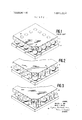
- FIG. 1 represents a prior art chip substrate module in which the connector joints are uniform;
- FIG. 2 is a planned view of a chip substrate module having larger volume outer connectors
- FIG. 3 is a planned view of a chip substrate module having larger volume inner connectors
- FIG. 4a is a planned view of a chip substrate module in which the solder wettable regions on the substrate are not of uniform size;
- FIG. 4b is a top view of the substrate of FIG. 4a.
- FIG. 5 is a planned view of a chip substrate module having solder and copper ball connector joints.
- FIG. 1 shows an example of a prior art flip chip connection using flexible solder balls.
- the chip l0 typically is a semiconductor material having passive and/or active circuit elements formed therein by known techniques.
- the surface 12 is typically covered by a passivating layer which is a good electrical insulator, and external electrical connections are made through the insulating layer to the active and passive devices by metallization areas 14 commonly referred to as ball limiting metallization or BLM.
- BLM ball limiting metallization
- the chip is mechanically and electrically connected to the substrate 16 by interconnecting means 20 which, in the case described herein, are solder joints.
- Electrically conductive fingers 22 on the substrate surface complete the electrical connection between chip and substrate.
- the method for forming the interconnection between chip and substrate is well known in the art and will not be discussed in detail herein, except to say that during the forming process, the module is heated sufficiently to cause the solder to melt and that the solder wettable area of the fingers 22 is limited to prevent the solder from flowing to an extent which will cause collapse of the chip on the substrate.
- the substrate itself is an insulator, usually a ceramic, and is not wettable with solder.
- Those portions of the fingers 22 which are to be closed off from the solder can be made of an electrically conductive metal which is not wettable with solder whereas the finger portion to be connected to the solder will be made of a material which is wettable with solder.
- the entire finger could be made from the same solder-wettable metal and the contact area confined by a glass dam which crosses the finger thereby preventing solder flow past the dam but not impairing the electrical conductivity between the solder contact area of the finger and the other area of the finger.
- the contact metallization on the substrate may come up through the substrate rather than extend to the edge as shown in FIG. 1. In such a case, the substrate itself will completely surround the contact area and the non-wettableness of the substrate will act as a complete barrier to the flow of the solder.
- the shape which the solder interconnections take on during the-heat-joining step is typically that of a partially squashed sphere such as that shown in FIG. I.
- the module In use, the module is subjected to temperature variations which cause expansion and contraction of the chip and substrate. The difference in expansion of the chip and substrate results in shear stress being placed on theinterconnector joints. The cyclic nature of the stress placed on the interconnector joints causes a fracture in the interconnector joints thereby impairing the electrical connection between chip and substrate.
- the present invention is concerned with the ability of the interconnectors to withstand the shear stress placed on them. Particularly, it has been found that there are significant advantages to be achieved, particularly the increased lifetime of the modules, if the interconnecting joints are designed so that they are not all alike, i.e., they-do not all have the same ability to resist shear stress.
- shear resistivity is used herein to designate the relative ability of an interconnecting joint to withstand shear stress, particularly cyclic shear stress, without fracturing.
- the volume of the four corner connectors is increased.
- the increased. volume of the solder tends to increase standoff, i.e., increase the distance between chip and substrate. This causes a stretching out or elongation of the other interconnection joints.
- the corner interconnection joints now have a different stress resistance than the intermediate joints.
- the increased volume of the corner pads will increase the stress resistance of the other pads, but the stress resistance of the corner pads will be decreased.
- the volume ratio of 2:1 will provide a module in which the fatter corner pads have a lower stress resistivity than the thinner inner pads. That means that given the identical stress conditions, the comer pads will fracture first.
- the module will have a neutral point which is determined by the positions of all the interconnecting joints.
- a module having all interconnecting joints on the periphery of a circle will have a neutral point at the center of the circle. Expansion takes place from the neutral point and consequently the greater the distance from the neutral point, the greater the stress placed on the joint.
- the corner pads would experience the greatest stress and would be the first to fracture if the stress resistivity of all joints is the same.
- the stress resistivity of the corner joints is less than that of the inner joints.
- the fatter corner joints could be dummyjoints, i.e., provide mechanical interconnection but not connected to any active or passive element in the chip.
- the thinner or more uniform shape of the interconnector pad means an increase in its ability to withstand stress. This is due to a more uniform strain distribution throughout the interconnection.
- the lower volume joints will have a more uniform shape and will have a greater stress resistance.
- the difference in volumes and the number ofjoints at the respective volumes could be such that the lower volume joints will be so stretched out that a more uniform strain distribution and consequently a greater stress resistivity will occur in the larger volume joints.
- the interconnecting joints 28 having the lower stress resistivity are the inner joints.
- the outer joints 30 have an increased stress resistivity.
- those joints which are subject to the greatest stress have the greatest ability to withstand stress at the expense of those joints which are subject to a lesser stress.
- there is no need for the fatter joints to be dummy joints all can be electrically active (i.e., connected to a passive or active element in the chip 10) with the consequence being an increased lifetime over the uniform stress resistivity module of FIG. 1.
- FIGS. 4a and 412 show the solder wettable area of the connector regions on the substrate, such as shown in FIGS. 4a and 412.
- FIG. 4a shows the module including chip 40, substrate 42 and interconnecting joints 76-84.
- FIG. 4b is a top view of the substrate 42 and illustrates the relative sizes of the connector regions.
- the difference in shape and therefore the difference in stress resistivity between the fat joints 82,84 and the thin joints 76,78,80 is not due to a difference in volume but due to a difference in size of the connector regions.
- a smaller connector region such as those shown at 62, 66, 70, and 74, causes the solder joint to bulge out and assume a fatter shape.
- the larger connector regions 60, 64, 68 and 72 result in a solder interconnection joint having a thinner shape.
- the difference in shape means a difference in stress resistivity.
- the outer joints, having the narrower cross section at the middle thereof, are subject to the greater amount of stress and are more able to withstand the stress than the inner fatter joints.
- the size of the connector regions may be limited by placing glass barriers across the fingers at appropriate spots or by using a non-wettable metal for the extended part of the fingers such as taught in the above mentioned patent to Miller. It will also be noted that the glass barrier or dams could be continuous for an entire side of the substrate or for all four sides thereof.
- the fatter interconnection joints may have a more uniform strain distribution than the thinner joints.
- variation in the stress resistance can be achieved by varying the material of the interconnectors, such as shown in FIG. 5.
- the joints 100, 102 and 104 are solder whereas the connectors 106 and 108 are copper ball connectors.
- Solder being a relatively ductile and flexible material, has a greater stress resistivity than the more rigid copper ball interconnectors.
- the copper ball being rigid, is better at providing standoff between chip and substrate.
- the rigid lower streess resistivity copper ball joints should be placed nearer the neutral point than the solder joints, or should be used as dummy joints.
- the ball In the upper ball joint, the ball itself is mechanically connected to the BLM and the conductive finger by small amounts of solder 105 and 107.
- each interconnecting joint there are two groups of interconnecting joints per module, each group having a different stress resistivity because of a difference in material (FIG. 5) or a difference in geometry (FIGS. 2-4), the latter difference being brought about by differences in volume, wettable finger size, or BLM size.
- FIG. 5 it is not necessary to limit the stress resistance variation for a module to two classes.
- An optimum design would be for each interconnection joint to have a stress resistance dependent upon the distance of the joint from the neutral point. In such a case, theoretically, all joints would fracture at the 'same time because the stress is also dependent on the distance from the neutral point.
- the optimum design would be for all joints to have stress resistance dependent on the position such that they all fail at the same time. While this is theoretically possible, it is difficult to achieve in practice. However, this condition can be approached and the fact that the stress resistance is dependent upon distance from the neutral point tends to equalize the failure time of the pads and improve the device overall.
- the staggering or gradation of the stress resistance of the joints can be achieved by staggering the volume, BLM or solder wettable areas.
- differences of the stress resistivity ofjoints in a single module need not be due to only one of the techniques outlined above, but can be due to any combination of techniques, i.e., varying volume, solder wettable finger size, BLM size and material.
- a semiconductor module formed of a chip mounted to a substrate each having first and second major surfaces the improvement comprising a plurality of solder wettable metal regions on the first major face of said chip,
- connection means have a first stress resistivity or a second stress resistivity different from the first dependent on whether connection is made to one of said first or second pluralities of wettable regions on said substrate.
- a semiconductor module comprising a first member having first and second major faces thereof, an electrically conductive material on portions of said first major face thereof, a second member having first and second major faces thereof, an electrically conductive pattern on said first major face of said second member including regions of wettable with solder conductive material differing in size and surrounded by nonwettable with solder material, and a plurality of stress resistant solder means for interconnecting and separating said electrically conductive material on said first member with respective ones of said surrounded solder wettable regions on said second member, whereby said solder means have differing stress resistivities dependent on which ones of said surrounded solder wettable regions connection is made to on said second member.
- solder means comprise the same volume of solder and wherein said solder means contacting said smaller surrounded solder wettable regions are fatter than said solder connectors contacting said larger surrounded solder wettable regions.
Abstract
The interconnecting joints between a semiconductor chip and a substrate are non-uniform in shape. The joints are solder and have varying shapes due to varying sizes of the solder wettable regions on the substrate. Smaller solder wettable regions cause the solder connectors to increase chip substrate standoff thereby relieving the stress on the remaining joints.
Description
United States Patent 1191 King eta1.
1 1 FLIP CHIP MODULE WITH NON-UNIFORM SOLDER WETTABLE AREAS ON THE SUBSTRATE [75] Inventors: William J. King, Poughkeepsie;
David L. Wilcox, Hopewell Junction, both of NY.
[73] Assignee: International Business Machines Corporation, Armonk, NY.
[22] Filed: Aug. 14, 1969 [21] Appl. No.: 850,093
[52] US. Cl 357/67, 357/65, 357/71, 29/588, 29/589 [51] Int. Cl. H011 3/00, H01] 5/00 8 Field of Search 317/234, 235, 5, 5.3, 5.2, 3l7/5.4; 29/587, 588, 589, 590, 578, 591, 626
[56] References Cited UNITED STATES PATENTS Burks 317/234 X Miller 317/234 X Merrin ct a1 317/234 X 3,458,925 8/1969 Napier ct a1. 317/234 X 3,470,611 10/1969 Mcivcr ct a1... 317/234 X 3,486,223 12/1969 Butera 317/234 X 3,488,840 1/1970 Hymes ct a1. 317/235 X OTHER PUBLICATIONS Bumps and Balls, Pillers and Beams, by G. Sideris;
Electronics June 28, 1965, pages 68 and 69.
Primary Examiner-Andrew .1. James Attorney, Agent, or Firm-John F. Osterndorf; Daniel E. [go
[57] ABSTRACT The interconnecting joints between a semiconductor chip and a substrate are non-uniform in shape. The joints are solder and have varying shapes due to varying sizes of the solder wettable regions on the substrate. Smaller solder wettable regions cause the solder connectors to increase chip substrate standoff thereby relieving the stress on the remaining joints.
8 Claims, 6 Drawing Figures PATENTEU MR1 H915 SHLEI 1 UP 2 1 PRIOR ART FLIP CHIP MODULE WITH NON-UNIFORM v SOLDER WETTABLE AREAS ON THE SUBSTRATE BACKGROUND OF THE INVENTION hundreds of elements, some means must be provided for connecting the elements on the chip to the outside world, e.g., other chips, power supply lines, etc. One well known techique comprises connecting the chip by interconnector joints to a substrate having a metallization pattern, e.g., conductive fingers, thereon. The conductive fingers extend to the edge of the substrate for connection to a larger connector board, e.g., mother board, which may accommodate many chips.
Electrical connection between the contact areas on the chip face, hereinafter sometimes referred to as BLM or ball limiting metallization, and corresponding contact areas on the substrate is provided by the connector joints. The joints also serve the mechanical function of supporting the chip and thereby separating the chip surface having the BLM areas from the substrate surface. In the absence of separation, the con ductive pattern on the substrate would shunt out some of the elements in the chip.
Rigid joints such as copper balls have been used, but their rigidity, while an advantage in maintaining standoff between chip and substrate, is a disadvantage from the standpoint of fatigue. A typical use of chip/substrate modules is in machines such as computers. The temperature changes between on and off states of the machine and the differences in thermal coefficients of expansion between the chip and substrate cause a shear stress to be placed on the connector joints. The thermal cycling causes fatigue and a fracture in the connector joint impairs the electrical connection and may disable an entire machine. The rigidity of the copper balls makes them more susceptible to fracture resulting from shear stresses than solder joints.
Ductile solder connectors provide greater resistance to stress because of their flexibility but were not originally thought to be satisfactory because of collapse during the heat-joining step.
A method of using ductile solder as connector joints wherein the solder joints do not collapse during the heat joining step is disclosed in US. Pat. No. 3,429,040 in the nameof Lewis F. Miller, issued Feb. 25, 1969 and assigned to the assignee of the present invention. As pointed out in the Miller patent, the wettable (with solder) area of the conductive fingers on the substrate is limited in size and surrounded by non-wettable material. The result is that the solder, when molten during the heat-joining step, is confined on the substrate to the wettable portion of the finger and due to surface tension maintains a shape which supports the chip above the substrate.
US. Pat. No. 3,436,818 issued Apr. 8, 1969 to Merrin, et al., and assigned to the assignee of the present application points out that collapse of the solder ball during heat-joining is also prevented if the conductive finger on the substrate is only partially wettable with solder. As described in the Merrin, et al., patent, the solder is placed on the BLM of the chip and heated, thereby assuming a hemispherical shape. The chip is placed face down on the substrate with the solder contacting the finger conductors at the proper designated position. The device is re-heated to cause joining of the solder pad to the fingers at the contact points. The flow of the solder is retarded by the partial wettability of the fingers, and because of this and surface tension the solder maintains a shape sufficient to support the chip.
Examples of solders and conductive materials for forming the ball limiting metallization on the chip and the fingers on the substrate are given in the abovementioned Miller and Merrin, et al., patents. Also, conductive materials which are wettable, partially wettable, and non-wettable with solder are mentioned.
The ability to prevent solder from collapsing during the heat joining step has provided the chip connector art with connectors that provide good electrical and mechanical connections, maintain standoff, and are relatively flexible and therefore able to withstand greater stress than rigid pads. Notwithstanding the usefulness of ductible solder balls or pads in the chip/substrate connector art, they are still subject to fracture caused by thermal cycling.
SUMMARY OF THE PRESENT INVENTION In accordance with the present invention, the life of a chip substrate module is increased by increasing the ability of at least some of the connector joints to withstand shear stress. The interconnection joints are designed so that not all are identical on the same chip. The differences, which can be differences in geometry or material, result in the connectors having different abilities to withstand stress. Those having the lesser ability to withstand stress are positioned at points of relatively low stress or serve as non-electrically active dummy points. In the latter case, they serve only a mechanical function and a fracture causing electrical conductivity impairment is of no consequence. Specifically, the chip-substrate module of the present invention is provided with different shaped solder connector joints. The difference in shape is brought about by a difference in size of the solder wettable areas on the substrate.
BRIEF DESCRIPTION OF THE DRAWINGS FIG. 1 represents a prior art chip substrate module in which the connector joints are uniform;
FIG. 2 is a planned view of a chip substrate module having larger volume outer connectors;
FIG. 3 is a planned view of a chip substrate module having larger volume inner connectors;
FIG. 4a is a planned view of a chip substrate module in which the solder wettable regions on the substrate are not of uniform size;
FIG. 4b is a top view of the substrate of FIG. 4a; and
FIG. 5 is a planned view of a chip substrate module having solder and copper ball connector joints.
FIG. 1 shows an example of a prior art flip chip connection using flexible solder balls. The chip l0 typically is a semiconductor material having passive and/or active circuit elements formed therein by known techniques. The surface 12 is typically covered by a passivating layer which is a good electrical insulator, and external electrical connections are made through the insulating layer to the active and passive devices by metallization areas 14 commonly referred to as ball limiting metallization or BLM.
The chip is mechanically and electrically connected to the substrate 16 by interconnecting means 20 which, in the case described herein, are solder joints. Electrically conductive fingers 22 on the substrate surface complete the electrical connection between chip and substrate. The method for forming the interconnection between chip and substrate is well known in the art and will not be discussed in detail herein, except to say that during the forming process, the module is heated sufficiently to cause the solder to melt and that the solder wettable area of the fingers 22 is limited to prevent the solder from flowing to an extent which will cause collapse of the chip on the substrate. The substrate itself is an insulator, usually a ceramic, and is not wettable with solder. Those portions of the fingers 22 which are to be closed off from the solder can be made of an electrically conductive metal which is not wettable with solder whereas the finger portion to be connected to the solder will be made of a material which is wettable with solder. Alternatively, the entire finger could be made from the same solder-wettable metal and the contact area confined by a glass dam which crosses the finger thereby preventing solder flow past the dam but not impairing the electrical conductivity between the solder contact area of the finger and the other area of the finger. Also, the contact metallization on the substrate may come up through the substrate rather than extend to the edge as shown in FIG. 1. In such a case, the substrate itself will completely surround the contact area and the non-wettableness of the substrate will act as a complete barrier to the flow of the solder.
The shape which the solder interconnections take on during the-heat-joining step is typically that of a partially squashed sphere such as that shown in FIG. I.
In use, the module is subjected to temperature variations which cause expansion and contraction of the chip and substrate. The difference in expansion of the chip and substrate results in shear stress being placed on theinterconnector joints. The cyclic nature of the stress placed on the interconnector joints causes a fracture in the interconnector joints thereby impairing the electrical connection between chip and substrate.
The present invention is concerned with the ability of the interconnectors to withstand the shear stress placed on them. Particularly, it has been found that there are significant advantages to be achieved, particularly the increased lifetime of the modules, if the interconnecting joints are designed so that they are not all alike, i.e., they-do not all have the same ability to resist shear stress. The term shear resistivity is used herein to designate the relative ability of an interconnecting joint to withstand shear stress, particularly cyclic shear stress, without fracturing.
In accordance with one embodiment of the present invention, shown in FIG. 2, the volume of the four corner connectors is increased. The increased. volume of the solder tends to increase standoff, i.e., increase the distance between chip and substrate. This causes a stretching out or elongation of the other interconnection joints. The corner interconnection joints now have a different stress resistance than the intermediate joints. The increased volume of the corner pads will increase the stress resistance of the other pads, but the stress resistance of the corner pads will be decreased. As an example, assuming uniform BLM size and finger size, the volume ratio of 2:1 will provide a module in which the fatter corner pads have a lower stress resistivity than the thinner inner pads. That means that given the identical stress conditions, the comer pads will fracture first.
The module will have a neutral point which is determined by the positions of all the interconnecting joints. As a simple example, a module having all interconnecting joints on the periphery of a circle will have a neutral point at the center of the circle. Expansion takes place from the neutral point and consequently the greater the distance from the neutral point, the greater the stress placed on the joint. For the arrangement shown in FIGS. 1 and 2, the corner pads would experience the greatest stress and would be the first to fracture if the stress resistivity of all joints is the same. In FIG. 2, the stress resistivity of the corner joints is less than that of the inner joints. However, the fatter corner joints could be dummyjoints, i.e., provide mechanical interconnection but not connected to any active or passive element in the chip. Under these circumstances, the advantages of increased stress resistance of the electrical interconnection joints (inner joints) is achieved. The fact that the corner joints will fracture sooner than in the case of FIG. 1 is not a detriment because the impairment of the electrical connection is of no consequence in a dummy joint.
It should be noted that the thinner or more uniform shape of the interconnector pad means an increase in its ability to withstand stress. This is due to a more uniform strain distribution throughout the interconnection. Typically, as pointed out above, the lower volume joints will have a more uniform shape and will have a greater stress resistance. However, it should be noted that in an extreme case, the difference in volumes and the number ofjoints at the respective volumes could be such that the lower volume joints will be so stretched out that a more uniform strain distribution and consequently a greater stress resistivity will occur in the larger volume joints. The important feature, however, that there is a difference in stress resistivity among interconnecting joints, is not impaired by this extreme case.
In the embodiment shown in FIG. 3, the interconnecting joints 28 having the lower stress resistivity are the inner joints. The outer joints 30 have an increased stress resistivity. Thus, those joints which are subject to the greatest stress have the greatest ability to withstand stress at the expense of those joints which are subject to a lesser stress. In this case, there is no need for the fatter joints to be dummy joints, all can be electrically active (i.e., connected to a passive or active element in the chip 10) with the consequence being an increased lifetime over the uniform stress resistivity module of FIG. 1.
One other method of varying the stress resistance of joints in a module is to vary the solder wettable area of the connector regions on the substrate, such as shown in FIGS. 4a and 412. FIG. 4a shows the module including chip 40, substrate 42 and interconnecting joints 76-84. FIG. 4b is a top view of the substrate 42 and illustrates the relative sizes of the connector regions.
In FIGS. 4a and 4b, the difference in shape and therefore the difference in stress resistivity between the fat joints 82,84 and the thin joints 76,78,80 is not due to a difference in volume but due to a difference in size of the connector regions. A smaller connector region, such as those shown at 62, 66, 70, and 74, causes the solder joint to bulge out and assume a fatter shape. The larger connector regions 60, 64, 68 and 72 result in a solder interconnection joint having a thinner shape. The difference in shape means a difference in stress resistivity. As shown in the drawing, the outer joints, having the narrower cross section at the middle thereof, are subject to the greater amount of stress and are more able to withstand the stress than the inner fatter joints.
The size of the connector regions may be limited by placing glass barriers across the fingers at appropriate spots or by using a non-wettable metal for the extended part of the fingers such as taught in the above mentioned patent to Miller. It will also be noted that the glass barrier or dams could be continuous for an entire side of the substrate or for all four sides thereof.
As in the case for volume variation, described above, it is not always the case that a smaller connector region on the substrate decreases the stress resistance of the solder interconnector. Because of the relative number of the large and small connector regions and the difference in size of these regions, along with the volume amount and the BLM size, the fatter interconnection joints may have a more uniform strain distribution than the thinner joints.
Another way in which variation of the joint geometry and concomitantly variation in the stress resistance can be achieved is by a variation in the size of the BLM on the chip.
Additionally, variation in the stress resistance can be achieved by varying the material of the interconnectors, such as shown in FIG. 5. There, the joints 100, 102 and 104 are solder whereas the connectors 106 and 108 are copper ball connectors. Solder, being a relatively ductile and flexible material, has a greater stress resistivity than the more rigid copper ball interconnectors. However, the copper ball, being rigid, is better at providing standoff between chip and substrate. With both types ofjoints used in the same module, the rigid lower streess resistivity copper ball joints should be placed nearer the neutral point than the solder joints, or should be used as dummy joints. In the upper ball joint, the ball itself is mechanically connected to the BLM and the conductive finger by small amounts of solder 105 and 107.
In each of the embodiments shown above, there are two groups of interconnecting joints per module, each group having a different stress resistivity because of a difference in material (FIG. 5) or a difference in geometry (FIGS. 2-4), the latter difference being brought about by differences in volume, wettable finger size, or BLM size. However, it is not necessary to limit the stress resistance variation for a module to two classes. An optimum design would be for each interconnection joint to have a stress resistance dependent upon the distance of the joint from the neutral point. In such a case, theoretically, all joints would fracture at the 'same time because the stress is also dependent on the distance from the neutral point.
It can be intuitively appreciated that, since the solder goes into a' molten state during the heat-joining step, and the surface tension holds the solder ball together,
an increase in volume of all of the solder balls would raise the height between chip and substrate. Conversely, a decrease in volume would lower the height. Furthermore, for a given volume of solder, the stress resistance is partially dependent on the height. Consequently, a mere lowering of the volume of the joints furthest from the neutral point (lowered from some optimum volume for a constant volume joint chip/substrate connection) would decrease the overall distance between chip and substrate thereby at least partially offsetting any increase in stress resistance due to the volume decrease.
Since the joints nearest the neutral point experience the least stress, their volume can. be increased without causing an earlier failure of the chip/substrate device. The increased volume of the inner joints offsets any standoff distance loss which would be caused by the decreased volume of the outer joints.
The optimum design would be for all joints to have stress resistance dependent on the position such that they all fail at the same time. While this is theoretically possible, it is difficult to achieve in practice. However, this condition can be approached and the fact that the stress resistance is dependent upon distance from the neutral point tends to equalize the failure time of the pads and improve the device overall. The staggering or gradation of the stress resistance of the joints can be achieved by staggering the volume, BLM or solder wettable areas.
It should be noted that differences of the stress resistivity ofjoints in a single module, need not be due to only one of the techniques outlined above, but can be due to any combination of techniques, i.e., varying volume, solder wettable finger size, BLM size and material.
What is claimed is:
1. In a semiconductor module formed of a chip mounted to a substrate each having first and second major surfaces the improvement comprising a plurality of solder wettable metal regions on the first major face of said chip,
a first plurality of solder wettable metal regions of a first size on the first major face of said substrate,
a second plurality of solder wettable metal regions of another size substantially different from the first size on said first major face of said substrate, and plural stress resistant solder means for connecting respective ones of the metal regions on said chip and substrate, whereby said connection means have a first stress resistivity or a second stress resistivity different from the first dependent on whether connection is made to one of said first or second pluralities of wettable regions on said substrate.
2. In the module as claimed in claim I wherein the first plurality of said solder wettable metal regions on said substrate are smaller in area than the second plurality of solder wettable metal regions on said substrate.
3. In the module as claimed in claim 2 wherein said second plurality of solder wettable metal regions are positioned near the corners of said module.
4. In the module as claimed in claim 2 wherein said first plurality of solder wettable metal regions are nearer the center of said chip than said second plurality of solder wettable metal regions.
5. In the module as claimed in claim 1 further comprising conductive metal fingers on said substrate in contact with said solder wettable regions and glass l dams overlying said conductive fingers to block solder on said solder wettable regions from flowing onto said conductive fingers.
6. A semiconductor module comprising a first member having first and second major faces thereof, an electrically conductive material on portions of said first major face thereof, a second member having first and second major faces thereof, an electrically conductive pattern on said first major face of said second member including regions of wettable with solder conductive material differing in size and surrounded by nonwettable with solder material, and a plurality of stress resistant solder means for interconnecting and separating said electrically conductive material on said first member with respective ones of said surrounded solder wettable regions on said second member, whereby said solder means have differing stress resistivities dependent on which ones of said surrounded solder wettable regions connection is made to on said second member.
7. The module as claimed in claim 6 wherein said surrounded solder wettable regions further from the center of said first member are larger than said other surrounded solder wettable regions.
8. The module as claimed in claim 6 wherein all of said solder means comprise the same volume of solder and wherein said solder means contacting said smaller surrounded solder wettable regions are fatter than said solder connectors contacting said larger surrounded solder wettable regions.
Claims (8)
1. In a semiconductor module formed of a chip mounted to a substrate each having first and second major surfaces the improvement comprising a plurality of solder wettable metal regions on the first major face of said chip, a first plurality of solder wettable metal regions of a first size on the first major face of said substrate, a second plurality of solder wettable metal regions of another size substantially different from the first size on said first major face of said substrate, and plural stress resistant solder means for connecting respective ones of the metal regions on said chip and substrate, whereby said connection means have a first stress resistivity or a second stress resistivity different from the first dependent on whether connection is made to one of said first or second pluralities of wettable regions on said substrate.
1. In a semiconductor module formed of a chip mounted to a substrate each having first and second major surfaces the improvement comprising a plurality of solder wettable metal regions on the first major face of said chip, a first plurality of solder wettable metal regions of a first size on the first major face of said substrate, a second plurality of solder wettable metal regions of another size substantially different from the first size on said first major face of said substrate, and plural stress resistant solder means for connecting respective ones of the metal regions on said chip and substrate, whereby said connection means have a first stress resistivity or a second stress resistivity different from the first dependent on whether connection is made to one of said first or second pluralities of wettable regions on said substrate.
2. In the module as claimed in claim 1 wherein the first plurality of said solder wettable metal regions on said substrate are smaller in area than the second plurality of solder wettable metal regions on said substrate.
3. In the module as claimed in claim 2 wherein said second plurality of solder wettable metal regions are positioned near the corners of said module.
4. In the module as claimed in claim 2 wherein said first plurality of solder wettable metal regions are nearer the center of said chip than said second plurality of solder wettable metal regions.
5. In the module as claimed in claim 1 further comprising conductive metal fingers on said substrate in contact with said solder wettable regions and glass dams overlying said conductive fingers to block solder on said solder wettable regions from flowing onto said conductive fingers.
6. A semiconductor module comprising a first member having first and second major faces thereof, an electrically conductive material on portions of said first major face thereof, a second member having first and second major faces thereof, an electrically conductive pattern on said first major face of said second member including regions of wettable with solder conductive material differing in size and surrounded by non-wettable with solder material, and a plurality of stress resistant solder means for interconnecting and separating said electrically conductive material on said first member with respective ones of said surrounded solder wettable regions on said second member, whereby said solder means have differing stress resistivities dependent on which ones of said surrounded solder wettable regions connection is made to on said second member.
7. The module as claimed in claim 6 wherein said surrounded solder wettable regions further from the center of said first member are larger than said other surrounded solder wettable regions.
Priority Applications (5)
| Application Number | Priority Date | Filing Date | Title |
|---|---|---|---|
| US850093A US3871014A (en) | 1969-08-14 | 1969-08-14 | Flip chip module with non-uniform solder wettable areas on the substrate |
| FR7022204A FR2057697A5 (en) | 1969-08-14 | 1970-06-17 | |
| DE19702031725 DE2031725C3 (en) | 1969-08-14 | 1970-06-26 | Device for connecting a semiconductor element to a carrier plate |
| GB35468/70A GB1298115A (en) | 1969-08-14 | 1970-07-22 | Electric circuit module |
| CA089,056A CA941980A (en) | 1969-08-14 | 1970-07-24 | Flip chip module with non-uniform solder wettable areas on the substrate |
Applications Claiming Priority (1)
| Application Number | Priority Date | Filing Date | Title |
|---|---|---|---|
| US850093A US3871014A (en) | 1969-08-14 | 1969-08-14 | Flip chip module with non-uniform solder wettable areas on the substrate |
Publications (1)
| Publication Number | Publication Date |
|---|---|
| US3871014A true US3871014A (en) | 1975-03-11 |
Family
ID=25307238
Family Applications (1)
| Application Number | Title | Priority Date | Filing Date |
|---|---|---|---|
| US850093A Expired - Lifetime US3871014A (en) | 1969-08-14 | 1969-08-14 | Flip chip module with non-uniform solder wettable areas on the substrate |
Country Status (2)
| Country | Link |
|---|---|
| US (1) | US3871014A (en) |
| CA (1) | CA941980A (en) |
Cited By (148)
| Publication number | Priority date | Publication date | Assignee | Title |
|---|---|---|---|---|
| DE2909370A1 (en) * | 1978-03-14 | 1979-09-20 | Citizen Watch Co Ltd | Semiconductor device with plastics, heat resistant substrate - has soldered integrated circuit chip and connecting solder beads, chip and substrate spacing being more than 60 microns |
| DE3042085A1 (en) * | 1979-11-12 | 1981-06-04 | Hitachi, Ltd., Tokyo | SEMICONDUCTOR BOARD ASSEMBLY AND METHOD FOR THE PRODUCTION THEREOF |
| WO1981001912A1 (en) * | 1979-12-26 | 1981-07-09 | Western Electric Co | Fabrication of circuit packages |
| DE3129568A1 (en) * | 1980-07-28 | 1982-04-22 | Hitachi, Ltd., Tokyo | Connection system of a semiconductor arrangement and method for manufacturing it |
| US4346396A (en) * | 1979-03-12 | 1982-08-24 | Western Electric Co., Inc. | Electronic device assembly and methods of making same |
| US4385310A (en) * | 1978-03-22 | 1983-05-24 | General Electric Company | Structured copper strain buffer |
| US4439918A (en) * | 1979-03-12 | 1984-04-03 | Western Electric Co., Inc. | Methods of packaging an electronic device |
| US4498096A (en) * | 1981-01-30 | 1985-02-05 | Motorola, Inc. | Button rectifier package for non-planar die |
| US4536786A (en) * | 1976-08-23 | 1985-08-20 | Sharp Kabushiki Kaisha | Lead electrode connection in a semiconductor device |
| US4673772A (en) * | 1984-10-05 | 1987-06-16 | Hitachi, Ltd. | Electronic circuit device and method of producing the same |
| US4774630A (en) * | 1985-09-30 | 1988-09-27 | Microelectronics Center Of North Carolina | Apparatus for mounting a semiconductor chip and making electrical connections thereto |
| US4892377A (en) * | 1987-08-19 | 1990-01-09 | Plessey Overseas Limited | Alignment of fibre arrays |
| US4942139A (en) * | 1988-02-01 | 1990-07-17 | General Instrument Corporation | Method of fabricating a brazed glass pre-passivated chip rectifier |
| US4951123A (en) * | 1988-09-30 | 1990-08-21 | Westinghouse Electric Corp. | Integrated circuit chip assembly utilizing selective backside deposition |
| US5007163A (en) * | 1990-04-18 | 1991-04-16 | International Business Machines Corporation | Non-destructure method of performing electrical burn-in testing of semiconductor chips |
| US5027189A (en) * | 1990-01-10 | 1991-06-25 | Hughes Aircraft Company | Integrated circuit solder die-attach design and method |
| US5111279A (en) * | 1989-08-28 | 1992-05-05 | Lsi Logic Corp. | Apparatus for isolation of flux materials in "flip-chip" manufacturing |
| US5160409A (en) * | 1991-08-05 | 1992-11-03 | Motorola, Inc. | Solder plate reflow method for forming a solder bump on a circuit trace intersection |
| US5166773A (en) * | 1989-07-03 | 1992-11-24 | General Electric Company | Hermetic package and packaged semiconductor chip having closely spaced leads extending through the package lid |
| US5168346A (en) * | 1989-08-28 | 1992-12-01 | Lsi Logic Corporation | Method and apparatus for isolation of flux materials in flip-chip manufacturing |
| US5186383A (en) * | 1991-10-02 | 1993-02-16 | Motorola, Inc. | Method for forming solder bump interconnections to a solder-plated circuit trace |
| US5194137A (en) * | 1991-08-05 | 1993-03-16 | Motorola Inc. | Solder plate reflow method for forming solder-bumped terminals |
| US5209390A (en) * | 1989-07-03 | 1993-05-11 | General Electric Company | Hermetic package and packaged semiconductor chip having closely spaced leads extending through the package lid |
| US5249098A (en) * | 1991-08-22 | 1993-09-28 | Lsi Logic Corporation | Semiconductor device package with solder bump electrical connections on an external surface of the package |
| US5269453A (en) * | 1992-04-02 | 1993-12-14 | Motorola, Inc. | Low temperature method for forming solder bump interconnections to a plated circuit trace |
| US5299730A (en) * | 1989-08-28 | 1994-04-05 | Lsi Logic Corporation | Method and apparatus for isolation of flux materials in flip-chip manufacturing |
| US5311060A (en) * | 1989-12-19 | 1994-05-10 | Lsi Logic Corporation | Heat sink for semiconductor device assembly |
| US5315485A (en) * | 1992-09-29 | 1994-05-24 | Mcnc | Variable size capture pads for multilayer ceramic substrates and connectors therefor |
| US5381307A (en) * | 1992-06-19 | 1995-01-10 | Motorola, Inc. | Self-aligning electrical contact array |
| US5384487A (en) * | 1993-05-05 | 1995-01-24 | Lsi Logic Corporation | Off-axis power branches for interior bond pad arrangements |
| US5388327A (en) * | 1993-09-15 | 1995-02-14 | Lsi Logic Corporation | Fabrication of a dissolvable film carrier containing conductive bump contacts for placement on a semiconductor device package |
| US5399903A (en) * | 1990-08-15 | 1995-03-21 | Lsi Logic Corporation | Semiconductor device having an universal die size inner lead layout |
| US5434750A (en) * | 1992-02-07 | 1995-07-18 | Lsi Logic Corporation | Partially-molded, PCB chip carrier package for certain non-square die shapes |
| US5438477A (en) * | 1993-08-12 | 1995-08-01 | Lsi Logic Corporation | Die-attach technique for flip-chip style mounting of semiconductor dies |
| US5453583A (en) * | 1993-05-05 | 1995-09-26 | Lsi Logic Corporation | Interior bond pad arrangements for alleviating thermal stresses |
| US5471090A (en) * | 1993-03-08 | 1995-11-28 | International Business Machines Corporation | Electronic structures having a joining geometry providing reduced capacitive loading |
| US5480834A (en) * | 1993-12-13 | 1996-01-02 | Micron Communications, Inc. | Process of manufacturing an electrical bonding interconnect having a metal bond pad portion and having a conductive epoxy portion comprising an oxide reducing agent |
| US5490040A (en) * | 1993-12-22 | 1996-02-06 | International Business Machines Corporation | Surface mount chip package having an array of solder ball contacts arranged in a circle and conductive pin contacts arranged outside the circular array |
| US5489804A (en) * | 1989-08-28 | 1996-02-06 | Lsi Logic Corporation | Flexible preformed planar structures for interposing between a chip and a substrate |
| US5504035A (en) * | 1989-08-28 | 1996-04-02 | Lsi Logic Corporation | Process for solder ball interconnecting a semiconductor device to a substrate using a noble metal foil embedded interposer substrate |
| US5567655A (en) * | 1993-05-05 | 1996-10-22 | Lsi Logic Corporation | Method for forming interior bond pads having zig-zag linear arrangement |
| US5637925A (en) * | 1988-02-05 | 1997-06-10 | Raychem Ltd | Uses of uniaxially electrically conductive articles |
| US5641946A (en) * | 1995-07-05 | 1997-06-24 | Anam Industrial Co., Ltd. | Method and circuit board structure for leveling solder balls in ball grid array semiconductor packages |
| US5770889A (en) * | 1995-12-29 | 1998-06-23 | Lsi Logic Corporation | Systems having advanced pre-formed planar structures |
| US5793116A (en) * | 1996-05-29 | 1998-08-11 | Mcnc | Microelectronic packaging using arched solder columns |
| US5812379A (en) * | 1996-08-13 | 1998-09-22 | Intel Corporation | Small diameter ball grid array pad size for improved motherboard routing |
| US5820014A (en) * | 1993-11-16 | 1998-10-13 | Form Factor, Inc. | Solder preforms |
| US5834799A (en) * | 1989-08-28 | 1998-11-10 | Lsi Logic | Optically transmissive preformed planar structures |
| US5849132A (en) * | 1992-09-15 | 1998-12-15 | Texas Instruments Incorporated | Ball contact for flip-chip devices |
| US5866951A (en) * | 1990-10-12 | 1999-02-02 | Robert Bosch Gmbh | Hybrid circuit with an electrically conductive adhesive |
| EP0899787A2 (en) * | 1997-07-25 | 1999-03-03 | Mcnc | Controlled-shaped solder reservoirs for increasing the volume of solder bumps, and structurs formed thereby |
| US5892179A (en) * | 1995-04-05 | 1999-04-06 | Mcnc | Solder bumps and structures for integrated redistribution routing conductors |
| US5914536A (en) * | 1995-07-07 | 1999-06-22 | Kabushiki Kaisha Toshiba | Semiconductor device and soldering portion inspecting method therefor |
| US5990472A (en) * | 1997-09-29 | 1999-11-23 | Mcnc | Microelectronic radiation detectors for detecting and emitting radiation signals |
| US5994152A (en) * | 1996-02-21 | 1999-11-30 | Formfactor, Inc. | Fabricating interconnects and tips using sacrificial substrates |
| US6096576A (en) * | 1997-09-02 | 2000-08-01 | Silicon Light Machines | Method of producing an electrical interface to an integrated circuit device having high density I/O count |
| US6133634A (en) * | 1998-08-05 | 2000-10-17 | Fairchild Semiconductor Corporation | High performance flip chip package |
| US6274474B1 (en) | 1999-10-25 | 2001-08-14 | International Business Machines Corporation | Method of forming BGA interconnections having mixed solder profiles |
| US6274823B1 (en) | 1993-11-16 | 2001-08-14 | Formfactor, Inc. | Interconnection substrates with resilient contact structures on both sides |
| US20010022382A1 (en) * | 1998-07-29 | 2001-09-20 | Shook James Gill | Method of and apparatus for sealing an hermetic lid to a semiconductor die |
| US6326696B1 (en) * | 1998-02-04 | 2001-12-04 | International Business Machines Corporation | Electronic package with interconnected chips |
| US6388203B1 (en) | 1995-04-04 | 2002-05-14 | Unitive International Limited | Controlled-shaped solder reservoirs for increasing the volume of solder bumps, and structures formed thereby |
| US6415974B2 (en) * | 2000-08-01 | 2002-07-09 | Siliconware Precision Industries Co., Ltd. | Structure of solder bumps with improved coplanarity and method of forming solder bumps with improved coplanarity |
| US6423623B1 (en) | 1998-06-09 | 2002-07-23 | Fairchild Semiconductor Corporation | Low Resistance package for semiconductor devices |
| US20020098610A1 (en) * | 2001-01-19 | 2002-07-25 | Alexander Payne | Reduced surface charging in silicon-based devices |
| US6443351B1 (en) * | 2000-05-15 | 2002-09-03 | Siliconware Precision Industries Co., Ltd. | Method of achieving solder ball coplanarity on ball grid array integrated circuit package |
| US20020186448A1 (en) * | 2001-04-10 | 2002-12-12 | Silicon Light Machines | Angled illumination for a single order GLV based projection system |
| US6498307B2 (en) * | 1998-03-11 | 2002-12-24 | Fujitsu Limited | Electronic component package, printing circuit board, and method of inspecting the printed circuit board |
| US20020196492A1 (en) * | 2001-06-25 | 2002-12-26 | Silicon Light Machines | Method and apparatus for dynamic equalization in wavelength division multiplexing |
| US20030001247A1 (en) * | 2001-06-18 | 2003-01-02 | International Rectifier Corporation | High voltage semiconductor device housing with increased clearance between housing can and die for improved flux flushing |
| US20030025984A1 (en) * | 2001-08-01 | 2003-02-06 | Chris Gudeman | Optical mem device with encapsulated dampening gas |
| US20030035189A1 (en) * | 2001-08-15 | 2003-02-20 | Amm David T. | Stress tuned blazed grating light valve |
| US20030035215A1 (en) * | 2001-08-15 | 2003-02-20 | Silicon Light Machines | Blazed grating light valve |
| US6541305B2 (en) | 2001-06-27 | 2003-04-01 | International Business Machines Corporation | Single-melt enhanced reliability solder element interconnect |
| US20030103194A1 (en) * | 2001-11-30 | 2003-06-05 | Gross Kenneth P. | Display apparatus including RGB color combiner and 1D light valve relay including schlieren filter |
| US20030132531A1 (en) * | 2001-03-28 | 2003-07-17 | Martin Standing | Surface mounted package with die bottom spaced from support board |
| US20030208753A1 (en) * | 2001-04-10 | 2003-11-06 | Silicon Light Machines | Method, system, and display apparatus for encrypted cinema |
| US20030214796A1 (en) * | 2002-05-20 | 2003-11-20 | Alps Electric Co., Ltd. | High frequency module mounting structure in which solder is prevented from peeling |
| US20030223675A1 (en) * | 2002-05-29 | 2003-12-04 | Silicon Light Machines | Optical switch |
| US20030235932A1 (en) * | 2002-05-28 | 2003-12-25 | Silicon Light Machines | Integrated driver process flow |
| US20040001264A1 (en) * | 2002-06-28 | 2004-01-01 | Christopher Gudeman | Micro-support structures |
| US20040001257A1 (en) * | 2001-03-08 | 2004-01-01 | Akira Tomita | High contrast grating light valve |
| US20040008399A1 (en) * | 2001-06-25 | 2004-01-15 | Trisnadi Jahja I. | Method, apparatus, and diffuser for reducing laser speckle |
| US20040057101A1 (en) * | 2002-06-28 | 2004-03-25 | James Hunter | Reduced formation of asperities in contact micro-structures |
| US6712480B1 (en) | 2002-09-27 | 2004-03-30 | Silicon Light Machines | Controlled curvature of stressed micro-structures |
| US6714337B1 (en) | 2002-06-28 | 2004-03-30 | Silicon Light Machines | Method and device for modulating a light beam and having an improved gamma response |
| US6728023B1 (en) | 2002-05-28 | 2004-04-27 | Silicon Light Machines | Optical device arrays with optimized image resolution |
| US20040099940A1 (en) * | 2002-11-22 | 2004-05-27 | International Rectifier Corporation | Semiconductor device having clips for connecting to external elements |
| US6800238B1 (en) | 2002-01-15 | 2004-10-05 | Silicon Light Machines, Inc. | Method for domain patterning in low coercive field ferroelectrics |
| US6801354B1 (en) | 2002-08-20 | 2004-10-05 | Silicon Light Machines, Inc. | 2-D diffraction grating for substantially eliminating polarization dependent losses |
| US6806997B1 (en) | 2003-02-28 | 2004-10-19 | Silicon Light Machines, Inc. | Patterned diffractive light modulator ribbon for PDL reduction |
| US6822797B1 (en) | 2002-05-31 | 2004-11-23 | Silicon Light Machines, Inc. | Light modulator structure for producing high-contrast operation using zero-order light |
| US6829077B1 (en) | 2003-02-28 | 2004-12-07 | Silicon Light Machines, Inc. | Diffractive light modulator with dynamically rotatable diffraction plane |
| US6829258B1 (en) | 2002-06-26 | 2004-12-07 | Silicon Light Machines, Inc. | Rapidly tunable external cavity laser |
| US6865346B1 (en) | 2001-06-05 | 2005-03-08 | Silicon Light Machines Corporation | Fiber optic transceiver |
| US6872984B1 (en) | 1998-07-29 | 2005-03-29 | Silicon Light Machines Corporation | Method of sealing a hermetic lid to a semiconductor die at an angle |
| DE10341206A1 (en) * | 2003-09-04 | 2005-04-14 | Infineon Technologies Ag | Appliance for improving reliability of BGA (ball grid array) solder connections between BGA component substrate, whose contact pads are fitted with solder balls or bumps |
| US20050136641A1 (en) * | 2003-10-14 | 2005-06-23 | Rinne Glenn A. | Solder structures for out of plane connections and related methods |
| US6922272B1 (en) | 2003-02-14 | 2005-07-26 | Silicon Light Machines Corporation | Method and apparatus for leveling thermal stress variations in multi-layer MEMS devices |
| US6922273B1 (en) | 2003-02-28 | 2005-07-26 | Silicon Light Machines Corporation | PDL mitigation structure for diffractive MEMS and gratings |
| US6927891B1 (en) | 2002-12-23 | 2005-08-09 | Silicon Light Machines Corporation | Tilt-able grating plane for improved crosstalk in 1×N blaze switches |
| US6928207B1 (en) | 2002-12-12 | 2005-08-09 | Silicon Light Machines Corporation | Apparatus for selectively blocking WDM channels |
| US6934070B1 (en) | 2002-12-18 | 2005-08-23 | Silicon Light Machines Corporation | Chirped optical MEM device |
| US20050186707A1 (en) * | 2000-04-04 | 2005-08-25 | International Rectifier Corp. | Chip scale surface mounted device and process of manufacture |
| US6947613B1 (en) | 2003-02-11 | 2005-09-20 | Silicon Light Machines Corporation | Wavelength selective switch and equalizer |
| US6956995B1 (en) | 2001-11-09 | 2005-10-18 | Silicon Light Machines Corporation | Optical communication arrangement |
| US6960828B2 (en) | 2002-06-25 | 2005-11-01 | Unitive International Limited | Electronic structures including conductive shunt layers |
| US6967412B2 (en) | 2001-08-24 | 2005-11-22 | International Rectifier Corporation | Wafer level underfill and interconnect process |
| US20050269677A1 (en) * | 2004-05-28 | 2005-12-08 | Martin Standing | Preparation of front contact for surface mounting |
| US20050279809A1 (en) * | 2000-11-10 | 2005-12-22 | Rinne Glenn A | Optical structures including liquid bumps and related methods |
| US6987600B1 (en) * | 2002-12-17 | 2006-01-17 | Silicon Light Machines Corporation | Arbitrary phase profile for better equalization in dynamic gain equalizer |
| US6991953B1 (en) | 2001-09-13 | 2006-01-31 | Silicon Light Machines Corporation | Microelectronic mechanical system and methods |
| US20060030139A1 (en) * | 2002-06-25 | 2006-02-09 | Mis J D | Methods of forming lead free solder bumps and related structures |
| US7027202B1 (en) | 2003-02-28 | 2006-04-11 | Silicon Light Machines Corp | Silicon substrate as a light modulator sacrificial layer |
| US20060076679A1 (en) * | 2002-06-25 | 2006-04-13 | Batchelor William E | Non-circular via holes for bumping pads and related structures |
| US7042611B1 (en) | 2003-03-03 | 2006-05-09 | Silicon Light Machines Corporation | Pre-deflected bias ribbons |
| US7054515B1 (en) | 2002-05-30 | 2006-05-30 | Silicon Light Machines Corporation | Diffractive light modulator-based dynamic equalizer with integrated spectral monitor |
| US7057795B2 (en) | 2002-08-20 | 2006-06-06 | Silicon Light Machines Corporation | Micro-structures with individually addressable ribbon pairs |
| US7057819B1 (en) | 2002-12-17 | 2006-06-06 | Silicon Light Machines Corporation | High contrast tilting ribbon blazed grating |
| US7068372B1 (en) | 2003-01-28 | 2006-06-27 | Silicon Light Machines Corporation | MEMS interferometer-based reconfigurable optical add-and-drop multiplexor |
| US20060205170A1 (en) * | 2005-03-09 | 2006-09-14 | Rinne Glenn A | Methods of forming self-healing metal-insulator-metal (MIM) structures and related devices |
| US7119447B2 (en) | 2001-03-28 | 2006-10-10 | International Rectifier Corporation | Direct fet device for high frequency application |
| US20060240598A1 (en) * | 2005-04-20 | 2006-10-26 | International Rectifier Corporation | Chip scale package |
| US20070012947A1 (en) * | 2002-07-15 | 2007-01-18 | International Rectifier Corporation | Direct FET device for high frequency application |
| US20070040282A1 (en) * | 2005-08-11 | 2007-02-22 | Samsung Electronics Co., Ltd. | Printed circuit board and method thereof and a solder ball land and method thereof |
| US20070182004A1 (en) * | 2006-02-08 | 2007-08-09 | Rinne Glenn A | Methods of Forming Electronic Interconnections Including Compliant Dielectric Layers and Related Devices |
| US7286764B1 (en) | 2003-02-03 | 2007-10-23 | Silicon Light Machines Corporation | Reconfigurable modulator-based optical add-and-drop multiplexer |
| US20080017797A1 (en) * | 2006-07-21 | 2008-01-24 | Zhaohui Cheng | Pattern inspection and measurement apparatus |
| US7358174B2 (en) | 2004-04-13 | 2008-04-15 | Amkor Technology, Inc. | Methods of forming solder bumps on exposed metal pads |
| US7368325B2 (en) | 2005-04-21 | 2008-05-06 | International Rectifier Corporation | Semiconductor package |
| US7391973B1 (en) | 2003-02-28 | 2008-06-24 | Silicon Light Machines Corporation | Two-stage gain equalizer |
| US7478741B1 (en) * | 2005-08-02 | 2009-01-20 | Sun Microsystems, Inc. | Solder interconnect integrity monitor |
| US7495326B2 (en) | 2002-10-22 | 2009-02-24 | Unitive International Limited | Stacked electronic structures including offset substrates |
| US20090057887A1 (en) * | 2007-08-29 | 2009-03-05 | Ati Technologies Ulc | Wafer level packaging of semiconductor chips |
| US7579697B2 (en) | 2002-07-15 | 2009-08-25 | International Rectifier Corporation | Arrangement for high frequency application |
| US20090236756A1 (en) * | 2008-03-19 | 2009-09-24 | Oh Han Kim | Flip chip interconnection system |
| US7601039B2 (en) | 1993-11-16 | 2009-10-13 | Formfactor, Inc. | Microelectronic contact structure and method of making same |
| US7674701B2 (en) | 2006-02-08 | 2010-03-09 | Amkor Technology, Inc. | Methods of forming metal layers using multi-layer lift-off patterns |
| USRE41559E1 (en) | 2001-10-10 | 2010-08-24 | International Rectifier Corporation | Semiconductor device package with improved cooling |
| US8033838B2 (en) | 1996-02-21 | 2011-10-11 | Formfactor, Inc. | Microelectronic contact structure |
| US20120286418A1 (en) * | 2011-05-13 | 2012-11-15 | Stats Chippac, Ltd. | Semiconductor Device and Method of Forming Dummy Pillars Between Semiconductor Die and Substrate for Maintaining Standoff Distance |
| US8373428B2 (en) | 1993-11-16 | 2013-02-12 | Formfactor, Inc. | Probe card assembly and kit, and methods of making same |
| US20130107484A1 (en) * | 2010-08-06 | 2013-05-02 | Panasonic Corporation | Circuit board and method for manufacturing same |
| US8466546B2 (en) | 2005-04-22 | 2013-06-18 | International Rectifier Corporation | Chip-scale package |
| US8674494B2 (en) | 2011-08-31 | 2014-03-18 | Samsung Electronics Co., Ltd. | Semiconductor package having supporting plate and method of forming the same |
| US20140322868A1 (en) * | 2012-11-14 | 2014-10-30 | Qualcomm Incorporated | Barrier layer on bump and non-wettable coating on trace |
| US9184144B2 (en) * | 2011-07-21 | 2015-11-10 | Qualcomm Incorporated | Interconnect pillars with directed compliance geometry |
| US20180019193A1 (en) * | 2016-07-18 | 2018-01-18 | Intel Corporation | Ball grid array (bga) with anchoring pins |
Citations (7)
| Publication number | Priority date | Publication date | Assignee | Title |
|---|---|---|---|---|
| US3380155A (en) * | 1965-05-12 | 1968-04-30 | Sprague Electric Co | Production of contact pads for semiconductors |
| US3429040A (en) * | 1965-06-18 | 1969-02-25 | Ibm | Method of joining a component to a substrate |
| US3436818A (en) * | 1965-12-13 | 1969-04-08 | Ibm | Method of fabricating a bonded joint |
| US3458925A (en) * | 1966-01-20 | 1969-08-05 | Ibm | Method of forming solder mounds on substrates |
| US3470611A (en) * | 1967-04-11 | 1969-10-07 | Corning Glass Works | Semiconductor device assembly method |
| US3486223A (en) * | 1967-04-27 | 1969-12-30 | Philco Ford Corp | Solder bonding |
| US3488840A (en) * | 1963-12-27 | 1970-01-13 | Ibm | Method of connecting microminiaturized devices to circuit panels |
-
1969
- 1969-08-14 US US850093A patent/US3871014A/en not_active Expired - Lifetime
-
1970
- 1970-07-24 CA CA089,056A patent/CA941980A/en not_active Expired
Patent Citations (7)
| Publication number | Priority date | Publication date | Assignee | Title |
|---|---|---|---|---|
| US3488840A (en) * | 1963-12-27 | 1970-01-13 | Ibm | Method of connecting microminiaturized devices to circuit panels |
| US3380155A (en) * | 1965-05-12 | 1968-04-30 | Sprague Electric Co | Production of contact pads for semiconductors |
| US3429040A (en) * | 1965-06-18 | 1969-02-25 | Ibm | Method of joining a component to a substrate |
| US3436818A (en) * | 1965-12-13 | 1969-04-08 | Ibm | Method of fabricating a bonded joint |
| US3458925A (en) * | 1966-01-20 | 1969-08-05 | Ibm | Method of forming solder mounds on substrates |
| US3470611A (en) * | 1967-04-11 | 1969-10-07 | Corning Glass Works | Semiconductor device assembly method |
| US3486223A (en) * | 1967-04-27 | 1969-12-30 | Philco Ford Corp | Solder bonding |
Cited By (225)
| Publication number | Priority date | Publication date | Assignee | Title |
|---|---|---|---|---|
| US4536786A (en) * | 1976-08-23 | 1985-08-20 | Sharp Kabushiki Kaisha | Lead electrode connection in a semiconductor device |
| DE2909370A1 (en) * | 1978-03-14 | 1979-09-20 | Citizen Watch Co Ltd | Semiconductor device with plastics, heat resistant substrate - has soldered integrated circuit chip and connecting solder beads, chip and substrate spacing being more than 60 microns |
| US4385310A (en) * | 1978-03-22 | 1983-05-24 | General Electric Company | Structured copper strain buffer |
| US4346396A (en) * | 1979-03-12 | 1982-08-24 | Western Electric Co., Inc. | Electronic device assembly and methods of making same |
| US4439918A (en) * | 1979-03-12 | 1984-04-03 | Western Electric Co., Inc. | Methods of packaging an electronic device |
| DE3042085A1 (en) * | 1979-11-12 | 1981-06-04 | Hitachi, Ltd., Tokyo | SEMICONDUCTOR BOARD ASSEMBLY AND METHOD FOR THE PRODUCTION THEREOF |
| WO1981001912A1 (en) * | 1979-12-26 | 1981-07-09 | Western Electric Co | Fabrication of circuit packages |
| US4352449A (en) * | 1979-12-26 | 1982-10-05 | Bell Telephone Laboratories, Incorporated | Fabrication of circuit packages |
| DE3129568A1 (en) * | 1980-07-28 | 1982-04-22 | Hitachi, Ltd., Tokyo | Connection system of a semiconductor arrangement and method for manufacturing it |
| US4498096A (en) * | 1981-01-30 | 1985-02-05 | Motorola, Inc. | Button rectifier package for non-planar die |
| US4673772A (en) * | 1984-10-05 | 1987-06-16 | Hitachi, Ltd. | Electronic circuit device and method of producing the same |
| US4774630A (en) * | 1985-09-30 | 1988-09-27 | Microelectronics Center Of North Carolina | Apparatus for mounting a semiconductor chip and making electrical connections thereto |
| US4892377A (en) * | 1987-08-19 | 1990-01-09 | Plessey Overseas Limited | Alignment of fibre arrays |
| US4942139A (en) * | 1988-02-01 | 1990-07-17 | General Instrument Corporation | Method of fabricating a brazed glass pre-passivated chip rectifier |
| US5637925A (en) * | 1988-02-05 | 1997-06-10 | Raychem Ltd | Uses of uniaxially electrically conductive articles |
| US4951123A (en) * | 1988-09-30 | 1990-08-21 | Westinghouse Electric Corp. | Integrated circuit chip assembly utilizing selective backside deposition |
| US5166773A (en) * | 1989-07-03 | 1992-11-24 | General Electric Company | Hermetic package and packaged semiconductor chip having closely spaced leads extending through the package lid |
| US5209390A (en) * | 1989-07-03 | 1993-05-11 | General Electric Company | Hermetic package and packaged semiconductor chip having closely spaced leads extending through the package lid |
| US5504035A (en) * | 1989-08-28 | 1996-04-02 | Lsi Logic Corporation | Process for solder ball interconnecting a semiconductor device to a substrate using a noble metal foil embedded interposer substrate |
| US5410805A (en) * | 1989-08-28 | 1995-05-02 | Lsi Logic Corporation | Method and apparatus for isolation of flux materials in "flip-chip" manufacturing |
| US5168346A (en) * | 1989-08-28 | 1992-12-01 | Lsi Logic Corporation | Method and apparatus for isolation of flux materials in flip-chip manufacturing |
| US5834799A (en) * | 1989-08-28 | 1998-11-10 | Lsi Logic | Optically transmissive preformed planar structures |
| US5489804A (en) * | 1989-08-28 | 1996-02-06 | Lsi Logic Corporation | Flexible preformed planar structures for interposing between a chip and a substrate |
| US5111279A (en) * | 1989-08-28 | 1992-05-05 | Lsi Logic Corp. | Apparatus for isolation of flux materials in "flip-chip" manufacturing |
| US5347162A (en) * | 1989-08-28 | 1994-09-13 | Lsi Logic Corporation | Preformed planar structures employing embedded conductors |
| US5299730A (en) * | 1989-08-28 | 1994-04-05 | Lsi Logic Corporation | Method and apparatus for isolation of flux materials in flip-chip manufacturing |
| US5311060A (en) * | 1989-12-19 | 1994-05-10 | Lsi Logic Corporation | Heat sink for semiconductor device assembly |
| US5027189A (en) * | 1990-01-10 | 1991-06-25 | Hughes Aircraft Company | Integrated circuit solder die-attach design and method |
| US5007163A (en) * | 1990-04-18 | 1991-04-16 | International Business Machines Corporation | Non-destructure method of performing electrical burn-in testing of semiconductor chips |
| US5399903A (en) * | 1990-08-15 | 1995-03-21 | Lsi Logic Corporation | Semiconductor device having an universal die size inner lead layout |
| US5866951A (en) * | 1990-10-12 | 1999-02-02 | Robert Bosch Gmbh | Hybrid circuit with an electrically conductive adhesive |
| US5194137A (en) * | 1991-08-05 | 1993-03-16 | Motorola Inc. | Solder plate reflow method for forming solder-bumped terminals |
| US5160409A (en) * | 1991-08-05 | 1992-11-03 | Motorola, Inc. | Solder plate reflow method for forming a solder bump on a circuit trace intersection |
| US5249098A (en) * | 1991-08-22 | 1993-09-28 | Lsi Logic Corporation | Semiconductor device package with solder bump electrical connections on an external surface of the package |
| US5186383A (en) * | 1991-10-02 | 1993-02-16 | Motorola, Inc. | Method for forming solder bump interconnections to a solder-plated circuit trace |
| US5434750A (en) * | 1992-02-07 | 1995-07-18 | Lsi Logic Corporation | Partially-molded, PCB chip carrier package for certain non-square die shapes |
| US5594626A (en) * | 1992-02-07 | 1997-01-14 | Lsi Logic Corporation | Partially-molded, PCB chip carrier package for certain non-square die shapes |
| US5269453A (en) * | 1992-04-02 | 1993-12-14 | Motorola, Inc. | Low temperature method for forming solder bump interconnections to a plated circuit trace |
| US5381307A (en) * | 1992-06-19 | 1995-01-10 | Motorola, Inc. | Self-aligning electrical contact array |
| US5849132A (en) * | 1992-09-15 | 1998-12-15 | Texas Instruments Incorporated | Ball contact for flip-chip devices |
| US5955784A (en) * | 1992-09-15 | 1999-09-21 | Texas Instruments Incorporated | Ball contact for flip-chip device |
| US5315485A (en) * | 1992-09-29 | 1994-05-24 | Mcnc | Variable size capture pads for multilayer ceramic substrates and connectors therefor |
| US5412537A (en) * | 1992-09-29 | 1995-05-02 | Mcnc | Electrical connector including variably spaced connector contacts |
| US5471090A (en) * | 1993-03-08 | 1995-11-28 | International Business Machines Corporation | Electronic structures having a joining geometry providing reduced capacitive loading |
| US5453583A (en) * | 1993-05-05 | 1995-09-26 | Lsi Logic Corporation | Interior bond pad arrangements for alleviating thermal stresses |
| US5384487A (en) * | 1993-05-05 | 1995-01-24 | Lsi Logic Corporation | Off-axis power branches for interior bond pad arrangements |
| US5567655A (en) * | 1993-05-05 | 1996-10-22 | Lsi Logic Corporation | Method for forming interior bond pads having zig-zag linear arrangement |
| US5438477A (en) * | 1993-08-12 | 1995-08-01 | Lsi Logic Corporation | Die-attach technique for flip-chip style mounting of semiconductor dies |
| US5388327A (en) * | 1993-09-15 | 1995-02-14 | Lsi Logic Corporation | Fabrication of a dissolvable film carrier containing conductive bump contacts for placement on a semiconductor device package |
| US5820014A (en) * | 1993-11-16 | 1998-10-13 | Form Factor, Inc. | Solder preforms |
| US7601039B2 (en) | 1993-11-16 | 2009-10-13 | Formfactor, Inc. | Microelectronic contact structure and method of making same |
| US8373428B2 (en) | 1993-11-16 | 2013-02-12 | Formfactor, Inc. | Probe card assembly and kit, and methods of making same |
| US6274823B1 (en) | 1993-11-16 | 2001-08-14 | Formfactor, Inc. | Interconnection substrates with resilient contact structures on both sides |
| US5804876A (en) * | 1993-12-13 | 1998-09-08 | Micron Communications Inc. | Electronic circuit bonding interconnect component and flip chip interconnect bond |
| US5480834A (en) * | 1993-12-13 | 1996-01-02 | Micron Communications, Inc. | Process of manufacturing an electrical bonding interconnect having a metal bond pad portion and having a conductive epoxy portion comprising an oxide reducing agent |
| US5663598A (en) * | 1993-12-13 | 1997-09-02 | Micron Communications, Inc. | Electrical circuit bonding interconnect component and flip chip interconnect bond |
| US6114239A (en) * | 1993-12-13 | 2000-09-05 | Micron Communications, Inc. | Electronic circuit bonding interconnect component and flip chip interconnect bond |
| US5490040A (en) * | 1993-12-22 | 1996-02-06 | International Business Machines Corporation | Surface mount chip package having an array of solder ball contacts arranged in a circle and conductive pin contacts arranged outside the circular array |
| US6392163B1 (en) | 1995-04-04 | 2002-05-21 | Unitive International Limited | Controlled-shaped solder reservoirs for increasing the volume of solder bumps |
| US6388203B1 (en) | 1995-04-04 | 2002-05-14 | Unitive International Limited | Controlled-shaped solder reservoirs for increasing the volume of solder bumps, and structures formed thereby |
| US6329608B1 (en) | 1995-04-05 | 2001-12-11 | Unitive International Limited | Key-shaped solder bumps and under bump metallurgy |
| US5892179A (en) * | 1995-04-05 | 1999-04-06 | Mcnc | Solder bumps and structures for integrated redistribution routing conductors |
| US6389691B1 (en) | 1995-04-05 | 2002-05-21 | Unitive International Limited | Methods for forming integrated redistribution routing conductors and solder bumps |
| US5641946A (en) * | 1995-07-05 | 1997-06-24 | Anam Industrial Co., Ltd. | Method and circuit board structure for leveling solder balls in ball grid array semiconductor packages |
| US5914536A (en) * | 1995-07-07 | 1999-06-22 | Kabushiki Kaisha Toshiba | Semiconductor device and soldering portion inspecting method therefor |
| US5770889A (en) * | 1995-12-29 | 1998-06-23 | Lsi Logic Corporation | Systems having advanced pre-formed planar structures |
| US5994152A (en) * | 1996-02-21 | 1999-11-30 | Formfactor, Inc. | Fabricating interconnects and tips using sacrificial substrates |
| US8033838B2 (en) | 1996-02-21 | 2011-10-11 | Formfactor, Inc. | Microelectronic contact structure |
| US5963793A (en) * | 1996-05-29 | 1999-10-05 | Mcnc | Microelectronic packaging using arched solder columns |
| US5793116A (en) * | 1996-05-29 | 1998-08-11 | Mcnc | Microelectronic packaging using arched solder columns |
| US5812379A (en) * | 1996-08-13 | 1998-09-22 | Intel Corporation | Small diameter ball grid array pad size for improved motherboard routing |
| SG99384A1 (en) * | 1997-07-25 | 2003-10-27 | Unitive Int Ltd | Controlled-shaped solder reservoirs for increasing the volume of solders bumps, and structures formed thereby |
| EP0899787A3 (en) * | 1997-07-25 | 2001-05-16 | Mcnc | Controlled-shaped solder reservoirs for increasing the volume of solder bumps, and structurs formed thereby |
| EP0899787A2 (en) * | 1997-07-25 | 1999-03-03 | Mcnc | Controlled-shaped solder reservoirs for increasing the volume of solder bumps, and structurs formed thereby |
| US6452260B1 (en) | 1997-09-02 | 2002-09-17 | Silicon Light Machines | Electrical interface to integrated circuit device having high density I/O count |
| US6096576A (en) * | 1997-09-02 | 2000-08-01 | Silicon Light Machines | Method of producing an electrical interface to an integrated circuit device having high density I/O count |
| US5990472A (en) * | 1997-09-29 | 1999-11-23 | Mcnc | Microelectronic radiation detectors for detecting and emitting radiation signals |
| US6326696B1 (en) * | 1998-02-04 | 2001-12-04 | International Business Machines Corporation | Electronic package with interconnected chips |
| US6727718B2 (en) | 1998-03-11 | 2004-04-27 | Fujistu Limited | Electronic component package, printed circuit board, and method of inspecting the printed circuit board |
| US6498307B2 (en) * | 1998-03-11 | 2002-12-24 | Fujitsu Limited | Electronic component package, printing circuit board, and method of inspecting the printed circuit board |
| US6423623B1 (en) | 1998-06-09 | 2002-07-23 | Fairchild Semiconductor Corporation | Low Resistance package for semiconductor devices |
| US20010022382A1 (en) * | 1998-07-29 | 2001-09-20 | Shook James Gill | Method of and apparatus for sealing an hermetic lid to a semiconductor die |
| US6872984B1 (en) | 1998-07-29 | 2005-03-29 | Silicon Light Machines Corporation | Method of sealing a hermetic lid to a semiconductor die at an angle |
| US6764875B2 (en) | 1998-07-29 | 2004-07-20 | Silicon Light Machines | Method of and apparatus for sealing an hermetic lid to a semiconductor die |
| US6294403B1 (en) | 1998-08-05 | 2001-09-25 | Rajeev Joshi | High performance flip chip package |
| US7892884B2 (en) | 1998-08-05 | 2011-02-22 | Fairchild Semiconductor Corporation | High performance multi-chip flip chip package |
| US6133634A (en) * | 1998-08-05 | 2000-10-17 | Fairchild Semiconductor Corporation | High performance flip chip package |
| US20090230540A1 (en) * | 1998-08-05 | 2009-09-17 | Rajeev Joshi | High performance multi-chip flip chip package |
| US7537958B1 (en) | 1998-08-05 | 2009-05-26 | Fairchild Semiconductor Corporation | High performance multi-chip flip chip package |
| US20040159939A1 (en) * | 1998-08-05 | 2004-08-19 | Fairchild Semiconductor Corporation | High performance multi-chip flip chip package |
| US6489678B1 (en) | 1998-08-05 | 2002-12-03 | Fairchild Semiconductor Corporation | High performance multi-chip flip chip package |
| US6992384B2 (en) | 1998-08-05 | 2006-01-31 | Fairchild Semiconductor Corporation | High performance multi-chip flip chip package |
| US6627991B1 (en) | 1998-08-05 | 2003-09-30 | Fairchild Semiconductor Corporation | High performance multi-chip flip package |
| US6541857B2 (en) * | 1999-10-25 | 2003-04-01 | International Business Machines Corporation | Method of forming BGA interconnections having mixed solder profiles |
| US6274474B1 (en) | 1999-10-25 | 2001-08-14 | International Business Machines Corporation | Method of forming BGA interconnections having mixed solder profiles |
| US20060220123A1 (en) * | 2000-04-04 | 2006-10-05 | International Rectifier Corporation | Chip scale surface mounted device and process of manufacture |
| US7122887B2 (en) | 2000-04-04 | 2006-10-17 | International Rectifier Corporation | Chip scale surface mounted device and process of manufacture |
| US20050186707A1 (en) * | 2000-04-04 | 2005-08-25 | International Rectifier Corp. | Chip scale surface mounted device and process of manufacture |
| US7253090B2 (en) | 2000-04-04 | 2007-08-07 | International Rectifier Corporation | Chip scale surface mounted device and process of manufacture |
| US7476979B2 (en) | 2000-04-04 | 2009-01-13 | International Rectifier Corporation | Chip scale surface mounted device and process of manufacture |
| US6443351B1 (en) * | 2000-05-15 | 2002-09-03 | Siliconware Precision Industries Co., Ltd. | Method of achieving solder ball coplanarity on ball grid array integrated circuit package |
| US6415974B2 (en) * | 2000-08-01 | 2002-07-09 | Siliconware Precision Industries Co., Ltd. | Structure of solder bumps with improved coplanarity and method of forming solder bumps with improved coplanarity |
| US7213740B2 (en) | 2000-11-10 | 2007-05-08 | Unitive International Limited | Optical structures including liquid bumps and related methods |
| US20050279809A1 (en) * | 2000-11-10 | 2005-12-22 | Rinne Glenn A | Optical structures including liquid bumps and related methods |
| US20070152020A1 (en) * | 2000-11-10 | 2007-07-05 | Unitive International Limited | Optical structures including liquid bumps |
| US20020098610A1 (en) * | 2001-01-19 | 2002-07-25 | Alexander Payne | Reduced surface charging in silicon-based devices |
| US20040001257A1 (en) * | 2001-03-08 | 2004-01-01 | Akira Tomita | High contrast grating light valve |
| US7177081B2 (en) | 2001-03-08 | 2007-02-13 | Silicon Light Machines Corporation | High contrast grating light valve type device |
| US7119447B2 (en) | 2001-03-28 | 2006-10-10 | International Rectifier Corporation | Direct fet device for high frequency application |
| US6930397B2 (en) | 2001-03-28 | 2005-08-16 | International Rectifier Corporation | Surface mounted package with die bottom spaced from support board |
| US7285866B2 (en) | 2001-03-28 | 2007-10-23 | International Rectifier Corporation | Surface mounted package with die bottom spaced from support board |
| US20030132531A1 (en) * | 2001-03-28 | 2003-07-17 | Martin Standing | Surface mounted package with die bottom spaced from support board |
| US20030208753A1 (en) * | 2001-04-10 | 2003-11-06 | Silicon Light Machines | Method, system, and display apparatus for encrypted cinema |
| US6707591B2 (en) | 2001-04-10 | 2004-03-16 | Silicon Light Machines | Angled illumination for a single order light modulator based projection system |
| US20020186448A1 (en) * | 2001-04-10 | 2002-12-12 | Silicon Light Machines | Angled illumination for a single order GLV based projection system |
| US6865346B1 (en) | 2001-06-05 | 2005-03-08 | Silicon Light Machines Corporation | Fiber optic transceiver |
| US7476964B2 (en) | 2001-06-18 | 2009-01-13 | International Rectifier Corporation | High voltage semiconductor device housing with increased clearance between housing can and die for improved flux flushing |
| US20030001247A1 (en) * | 2001-06-18 | 2003-01-02 | International Rectifier Corporation | High voltage semiconductor device housing with increased clearance between housing can and die for improved flux flushing |
| US6782205B2 (en) | 2001-06-25 | 2004-08-24 | Silicon Light Machines | Method and apparatus for dynamic equalization in wavelength division multiplexing |
| US20020196492A1 (en) * | 2001-06-25 | 2002-12-26 | Silicon Light Machines | Method and apparatus for dynamic equalization in wavelength division multiplexing |
| US6747781B2 (en) | 2001-06-25 | 2004-06-08 | Silicon Light Machines, Inc. | Method, apparatus, and diffuser for reducing laser speckle |
| US20040008399A1 (en) * | 2001-06-25 | 2004-01-15 | Trisnadi Jahja I. | Method, apparatus, and diffuser for reducing laser speckle |
| US6541305B2 (en) | 2001-06-27 | 2003-04-01 | International Business Machines Corporation | Single-melt enhanced reliability solder element interconnect |
| US20030025984A1 (en) * | 2001-08-01 | 2003-02-06 | Chris Gudeman | Optical mem device with encapsulated dampening gas |
| US20030035215A1 (en) * | 2001-08-15 | 2003-02-20 | Silicon Light Machines | Blazed grating light valve |
| US6829092B2 (en) * | 2001-08-15 | 2004-12-07 | Silicon Light Machines, Inc. | Blazed grating light valve |
| US20030035189A1 (en) * | 2001-08-15 | 2003-02-20 | Amm David T. | Stress tuned blazed grating light valve |
| US20030223116A1 (en) * | 2001-08-15 | 2003-12-04 | Amm David T. | Blazed grating light valve |
| US6967412B2 (en) | 2001-08-24 | 2005-11-22 | International Rectifier Corporation | Wafer level underfill and interconnect process |
| US6991953B1 (en) | 2001-09-13 | 2006-01-31 | Silicon Light Machines Corporation | Microelectronic mechanical system and methods |
| US7049164B2 (en) | 2001-09-13 | 2006-05-23 | Silicon Light Machines Corporation | Microelectronic mechanical system and methods |
| USRE41559E1 (en) | 2001-10-10 | 2010-08-24 | International Rectifier Corporation | Semiconductor device package with improved cooling |
| US6956995B1 (en) | 2001-11-09 | 2005-10-18 | Silicon Light Machines Corporation | Optical communication arrangement |
| US20030103194A1 (en) * | 2001-11-30 | 2003-06-05 | Gross Kenneth P. | Display apparatus including RGB color combiner and 1D light valve relay including schlieren filter |
| US6800238B1 (en) | 2002-01-15 | 2004-10-05 | Silicon Light Machines, Inc. | Method for domain patterning in low coercive field ferroelectrics |
| US6950315B2 (en) * | 2002-05-20 | 2005-09-27 | Alps Electric Co., Ltd. | High frequency module mounting structure in which solder is prevented from peeling |
| US20030214796A1 (en) * | 2002-05-20 | 2003-11-20 | Alps Electric Co., Ltd. | High frequency module mounting structure in which solder is prevented from peeling |
| US6728023B1 (en) | 2002-05-28 | 2004-04-27 | Silicon Light Machines | Optical device arrays with optimized image resolution |
| US6767751B2 (en) | 2002-05-28 | 2004-07-27 | Silicon Light Machines, Inc. | Integrated driver process flow |
| US20030235932A1 (en) * | 2002-05-28 | 2003-12-25 | Silicon Light Machines | Integrated driver process flow |
| US20030223675A1 (en) * | 2002-05-29 | 2003-12-04 | Silicon Light Machines | Optical switch |
| US7054515B1 (en) | 2002-05-30 | 2006-05-30 | Silicon Light Machines Corporation | Diffractive light modulator-based dynamic equalizer with integrated spectral monitor |
| US6822797B1 (en) | 2002-05-31 | 2004-11-23 | Silicon Light Machines, Inc. | Light modulator structure for producing high-contrast operation using zero-order light |
| US7879715B2 (en) | 2002-06-25 | 2011-02-01 | Unitive International Limited | Methods of forming electronic structures including conductive shunt layers and related structures |
| US7839000B2 (en) | 2002-06-25 | 2010-11-23 | Unitive International Limited | Solder structures including barrier layers with nickel and/or copper |
| US7297631B2 (en) | 2002-06-25 | 2007-11-20 | Unitive International Limited | Methods of forming electronic structures including conductive shunt layers and related structures |
| US7547623B2 (en) | 2002-06-25 | 2009-06-16 | Unitive International Limited | Methods of forming lead free solder bumps |
| US7531898B2 (en) | 2002-06-25 | 2009-05-12 | Unitive International Limited | Non-Circular via holes for bumping pads and related structures |
| US20060030139A1 (en) * | 2002-06-25 | 2006-02-09 | Mis J D | Methods of forming lead free solder bumps and related structures |
| US20080026560A1 (en) * | 2002-06-25 | 2008-01-31 | Unitive International Limited | Methods of forming electronic structures including conductive shunt layers and related structures |
| US20060076679A1 (en) * | 2002-06-25 | 2006-04-13 | Batchelor William E | Non-circular via holes for bumping pads and related structures |
| US20110084392A1 (en) * | 2002-06-25 | 2011-04-14 | Nair Krishna K | Electronic Structures Including Conductive Layers Comprising Copper and Having a Thickness of at Least 0.5 Micrometers |
| US20060009023A1 (en) * | 2002-06-25 | 2006-01-12 | Unitive International Limited | Methods of forming electronic structures including conductive shunt layers and related structures |
| US8294269B2 (en) | 2002-06-25 | 2012-10-23 | Unitive International | Electronic structures including conductive layers comprising copper and having a thickness of at least 0.5 micrometers |
| US20090212427A1 (en) * | 2002-06-25 | 2009-08-27 | Unitive International Limited | Solder Structures Including Barrier Layers with Nickel and/or Copper |
| US6960828B2 (en) | 2002-06-25 | 2005-11-01 | Unitive International Limited | Electronic structures including conductive shunt layers |
| US6829258B1 (en) | 2002-06-26 | 2004-12-07 | Silicon Light Machines, Inc. | Rapidly tunable external cavity laser |
| US20040057101A1 (en) * | 2002-06-28 | 2004-03-25 | James Hunter | Reduced formation of asperities in contact micro-structures |
| US6908201B2 (en) | 2002-06-28 | 2005-06-21 | Silicon Light Machines Corporation | Micro-support structures |
| US20040001264A1 (en) * | 2002-06-28 | 2004-01-01 | Christopher Gudeman | Micro-support structures |
| US6714337B1 (en) | 2002-06-28 | 2004-03-30 | Silicon Light Machines | Method and device for modulating a light beam and having an improved gamma response |
| US6813059B2 (en) | 2002-06-28 | 2004-11-02 | Silicon Light Machines, Inc. | Reduced formation of asperities in contact micro-structures |
| US20070012947A1 (en) * | 2002-07-15 | 2007-01-18 | International Rectifier Corporation | Direct FET device for high frequency application |
| US7397137B2 (en) | 2002-07-15 | 2008-07-08 | International Rectifier Corporation | Direct FET device for high frequency application |
| US7579697B2 (en) | 2002-07-15 | 2009-08-25 | International Rectifier Corporation | Arrangement for high frequency application |
| US7057795B2 (en) | 2002-08-20 | 2006-06-06 | Silicon Light Machines Corporation | Micro-structures with individually addressable ribbon pairs |
| US6801354B1 (en) | 2002-08-20 | 2004-10-05 | Silicon Light Machines, Inc. | 2-D diffraction grating for substantially eliminating polarization dependent losses |
| US6712480B1 (en) | 2002-09-27 | 2004-03-30 | Silicon Light Machines | Controlled curvature of stressed micro-structures |
| US7495326B2 (en) | 2002-10-22 | 2009-02-24 | Unitive International Limited | Stacked electronic structures including offset substrates |
| US6841865B2 (en) | 2002-11-22 | 2005-01-11 | International Rectifier Corporation | Semiconductor device having clips for connecting to external elements |
| US20040099940A1 (en) * | 2002-11-22 | 2004-05-27 | International Rectifier Corporation | Semiconductor device having clips for connecting to external elements |
| US6928207B1 (en) | 2002-12-12 | 2005-08-09 | Silicon Light Machines Corporation | Apparatus for selectively blocking WDM channels |
| US6987600B1 (en) * | 2002-12-17 | 2006-01-17 | Silicon Light Machines Corporation | Arbitrary phase profile for better equalization in dynamic gain equalizer |
| US7057819B1 (en) | 2002-12-17 | 2006-06-06 | Silicon Light Machines Corporation | High contrast tilting ribbon blazed grating |
| US6934070B1 (en) | 2002-12-18 | 2005-08-23 | Silicon Light Machines Corporation | Chirped optical MEM device |
| US6927891B1 (en) | 2002-12-23 | 2005-08-09 | Silicon Light Machines Corporation | Tilt-able grating plane for improved crosstalk in 1×N blaze switches |
| US7068372B1 (en) | 2003-01-28 | 2006-06-27 | Silicon Light Machines Corporation | MEMS interferometer-based reconfigurable optical add-and-drop multiplexor |
| US7286764B1 (en) | 2003-02-03 | 2007-10-23 | Silicon Light Machines Corporation | Reconfigurable modulator-based optical add-and-drop multiplexer |
| US6947613B1 (en) | 2003-02-11 | 2005-09-20 | Silicon Light Machines Corporation | Wavelength selective switch and equalizer |
| US6922272B1 (en) | 2003-02-14 | 2005-07-26 | Silicon Light Machines Corporation | Method and apparatus for leveling thermal stress variations in multi-layer MEMS devices |
| US6922273B1 (en) | 2003-02-28 | 2005-07-26 | Silicon Light Machines Corporation | PDL mitigation structure for diffractive MEMS and gratings |
| US7027202B1 (en) | 2003-02-28 | 2006-04-11 | Silicon Light Machines Corp | Silicon substrate as a light modulator sacrificial layer |
| US6806997B1 (en) | 2003-02-28 | 2004-10-19 | Silicon Light Machines, Inc. | Patterned diffractive light modulator ribbon for PDL reduction |
| US7391973B1 (en) | 2003-02-28 | 2008-06-24 | Silicon Light Machines Corporation | Two-stage gain equalizer |
| US6829077B1 (en) | 2003-02-28 | 2004-12-07 | Silicon Light Machines, Inc. | Diffractive light modulator with dynamically rotatable diffraction plane |
| US7042611B1 (en) | 2003-03-03 | 2006-05-09 | Silicon Light Machines Corporation | Pre-deflected bias ribbons |
| DE10341206A1 (en) * | 2003-09-04 | 2005-04-14 | Infineon Technologies Ag | Appliance for improving reliability of BGA (ball grid array) solder connections between BGA component substrate, whose contact pads are fitted with solder balls or bumps |
| US7049216B2 (en) | 2003-10-14 | 2006-05-23 | Unitive International Limited | Methods of providing solder structures for out plane connections |
| US20060138675A1 (en) * | 2003-10-14 | 2006-06-29 | Rinne Glenn A | Solder structures for out of plane connections |
| US20050136641A1 (en) * | 2003-10-14 | 2005-06-23 | Rinne Glenn A. | Solder structures for out of plane connections and related methods |
| US7659621B2 (en) | 2003-10-14 | 2010-02-09 | Unitive International Limited | Solder structures for out of plane connections |
| US7358174B2 (en) | 2004-04-13 | 2008-04-15 | Amkor Technology, Inc. | Methods of forming solder bumps on exposed metal pads |
| US20050269677A1 (en) * | 2004-05-28 | 2005-12-08 | Martin Standing | Preparation of front contact for surface mounting |
| US20060205170A1 (en) * | 2005-03-09 | 2006-09-14 | Rinne Glenn A | Methods of forming self-healing metal-insulator-metal (MIM) structures and related devices |
| US20060240598A1 (en) * | 2005-04-20 | 2006-10-26 | International Rectifier Corporation | Chip scale package |
| US20090174058A1 (en) * | 2005-04-20 | 2009-07-09 | International Rectifier Corporation | Chip scale package |
| US7524701B2 (en) | 2005-04-20 | 2009-04-28 | International Rectifier Corporation | Chip-scale package |
| US8097938B2 (en) | 2005-04-20 | 2012-01-17 | International Rectifier Corporation | Conductive chip-scale package |
| US8061023B2 (en) | 2005-04-21 | 2011-11-22 | International Rectifier Corporation | Process of fabricating a semiconductor package |
| US7368325B2 (en) | 2005-04-21 | 2008-05-06 | International Rectifier Corporation | Semiconductor package |
| US8466546B2 (en) | 2005-04-22 | 2013-06-18 | International Rectifier Corporation | Chip-scale package |
| US7478741B1 (en) * | 2005-08-02 | 2009-01-20 | Sun Microsystems, Inc. | Solder interconnect integrity monitor |
| US8039972B2 (en) * | 2005-08-11 | 2011-10-18 | Samsung Electronics Co., Ltd. | Printed circuit board and method thereof and a solder ball land and method thereof |
| US20090278249A1 (en) * | 2005-08-11 | 2009-11-12 | Ky-Hyun Jung | Printed circuit board and method thereof and a solder ball land and method thereof |
| US7576438B2 (en) * | 2005-08-11 | 2009-08-18 | Samsung Electronics Co., Ltd. | Printed circuit board and method thereof and a solder ball land and method thereof |
| US20070040282A1 (en) * | 2005-08-11 | 2007-02-22 | Samsung Electronics Co., Ltd. | Printed circuit board and method thereof and a solder ball land and method thereof |
| US20070182004A1 (en) * | 2006-02-08 | 2007-08-09 | Rinne Glenn A | Methods of Forming Electronic Interconnections Including Compliant Dielectric Layers and Related Devices |
| US7932615B2 (en) | 2006-02-08 | 2011-04-26 | Amkor Technology, Inc. | Electronic devices including solder bumps on compliant dielectric layers |
| US7674701B2 (en) | 2006-02-08 | 2010-03-09 | Amkor Technology, Inc. | Methods of forming metal layers using multi-layer lift-off patterns |
| US20080017797A1 (en) * | 2006-07-21 | 2008-01-24 | Zhaohui Cheng | Pattern inspection and measurement apparatus |
| US20090057887A1 (en) * | 2007-08-29 | 2009-03-05 | Ati Technologies Ulc | Wafer level packaging of semiconductor chips |
| US8344505B2 (en) * | 2007-08-29 | 2013-01-01 | Ati Technologies Ulc | Wafer level packaging of semiconductor chips |
| US8785317B2 (en) | 2007-08-29 | 2014-07-22 | Ati Technologies Ulc | Wafer level packaging of semiconductor chips |
| US20090236756A1 (en) * | 2008-03-19 | 2009-09-24 | Oh Han Kim | Flip chip interconnection system |
| US8604624B2 (en) | 2008-03-19 | 2013-12-10 | Stats Chippac Ltd. | Flip chip interconnection system having solder position control mechanism |
| US20130107484A1 (en) * | 2010-08-06 | 2013-05-02 | Panasonic Corporation | Circuit board and method for manufacturing same |
| US9198284B2 (en) * | 2010-08-06 | 2015-11-24 | Panasonic Intellectual Property Management Co., Ltd. | Circuit board and method for manufacturing same |
| US20120286418A1 (en) * | 2011-05-13 | 2012-11-15 | Stats Chippac, Ltd. | Semiconductor Device and Method of Forming Dummy Pillars Between Semiconductor Die and Substrate for Maintaining Standoff Distance |
| US10096540B2 (en) * | 2011-05-13 | 2018-10-09 | STATS ChipPAC Pte. Ltd. | Semiconductor device and method of forming dummy pillars between semiconductor die and substrate for maintaining standoff distance |
| US9184144B2 (en) * | 2011-07-21 | 2015-11-10 | Qualcomm Incorporated | Interconnect pillars with directed compliance geometry |
| US8674494B2 (en) | 2011-08-31 | 2014-03-18 | Samsung Electronics Co., Ltd. | Semiconductor package having supporting plate and method of forming the same |
| US9412720B2 (en) | 2011-08-31 | 2016-08-09 | Samsung Electronics Co., Ltd. | Semiconductor package having supporting plate and method of forming the same |
| US20140322868A1 (en) * | 2012-11-14 | 2014-10-30 | Qualcomm Incorporated | Barrier layer on bump and non-wettable coating on trace |
| US20180019193A1 (en) * | 2016-07-18 | 2018-01-18 | Intel Corporation | Ball grid array (bga) with anchoring pins |
| US9953909B2 (en) * | 2016-07-18 | 2018-04-24 | Intel Corporation | Ball grid array (BGA) with anchoring pins |
Also Published As
| Publication number | Publication date |
|---|---|
| CA941980A (en) | 1974-02-12 |
Similar Documents
| Publication | Publication Date | Title |
|---|---|---|
| US3871014A (en) | Flip chip module with non-uniform solder wettable areas on the substrate | |
| US3871015A (en) | Flip chip module with non-uniform connector joints | |
| KR100247716B1 (en) | Structurally reinforced ball grid array semiconductor package and systems | |
| US5706174A (en) | Compliant microelectrionic mounting device | |
| US5349495A (en) | System for securing and electrically connecting a semiconductor chip to a substrate | |
| US5477082A (en) | Bi-planar multi-chip module | |
| EP0197089B1 (en) | Wafer-scale-integrated assembly | |
| JP3084230B2 (en) | Ball grid array package | |
| KR100385766B1 (en) | Semiconductor device having resin members provided separately corresponding to externally connecting electrodes | |
| KR970024069A (en) | SEMICONDUCTOR DEVICE AND METHOD OF MANUFACTURING SEMICONDUCTOR DEVICE | |
| US7663248B2 (en) | Flip-chip component | |
| KR100834441B1 (en) | Semiconductor device and package comprising the same | |
| JP2001168131A (en) | Thin interconnection structure | |
| US5959348A (en) | Construction of PBGA substrate for flip chip packing | |
| US7227268B2 (en) | Placement of sacrificial solder balls underneath the PBGA substrate | |
| KR100499821B1 (en) | An integrated circuit carrier | |
| KR100538160B1 (en) | A multi-chip integrated circuit carrier | |
| US6943103B2 (en) | Methods for reducing flip chip stress | |
| KR100526330B1 (en) | Integrated circuit carrier with recesses | |
| US6255599B1 (en) | Relocating the neutral plane in a PBGA substrate to eliminate chip crack and interfacial delamination | |
| US7601612B1 (en) | Method for forming solder joints for a flip chip assembly | |
| EP1970962B1 (en) | Semiconductor device | |
| JPS6019658B2 (en) | Semiconductor device mounting structure | |
| US20230230889A1 (en) | Interconnection array device with support | |
| JP3016380B2 (en) | Semiconductor device |