US4170419A - Optical web inspection system - Google Patents
Optical web inspection system Download PDFInfo
- Publication number
- US4170419A US4170419A US05/771,103 US77110377A US4170419A US 4170419 A US4170419 A US 4170419A US 77110377 A US77110377 A US 77110377A US 4170419 A US4170419 A US 4170419A
- Authority
- US
- United States
- Prior art keywords
- web
- output
- memory
- fabric
- signal
- Prior art date
- Legal status (The legal status is an assumption and is not a legal conclusion. Google has not performed a legal analysis and makes no representation as to the accuracy of the status listed.)
- Expired - Lifetime
Links
Images


Classifications
-
- G—PHYSICS
- G01—MEASURING; TESTING
- G01N—INVESTIGATING OR ANALYSING MATERIALS BY DETERMINING THEIR CHEMICAL OR PHYSICAL PROPERTIES
- G01N21/00—Investigating or analysing materials by the use of optical means, i.e. using sub-millimetre waves, infrared, visible or ultraviolet light
- G01N21/84—Systems specially adapted for particular applications
- G01N21/88—Investigating the presence of flaws or contamination
- G01N21/89—Investigating the presence of flaws or contamination in moving material, e.g. running paper or textiles
- G01N21/8914—Investigating the presence of flaws or contamination in moving material, e.g. running paper or textiles characterised by the material examined
- G01N21/8915—Investigating the presence of flaws or contamination in moving material, e.g. running paper or textiles characterised by the material examined non-woven textile material
-
- G—PHYSICS
- G01—MEASURING; TESTING
- G01N—INVESTIGATING OR ANALYSING MATERIALS BY DETERMINING THEIR CHEMICAL OR PHYSICAL PROPERTIES
- G01N21/00—Investigating or analysing materials by the use of optical means, i.e. using sub-millimetre waves, infrared, visible or ultraviolet light
- G01N21/84—Systems specially adapted for particular applications
- G01N21/88—Investigating the presence of flaws or contamination
- G01N21/89—Investigating the presence of flaws or contamination in moving material, e.g. running paper or textiles
- G01N21/892—Investigating the presence of flaws or contamination in moving material, e.g. running paper or textiles characterised by the flaw, defect or object feature examined
- G01N21/898—Irregularities in textured or patterned surfaces, e.g. textiles, wood
- G01N21/8983—Irregularities in textured or patterned surfaces, e.g. textiles, wood for testing textile webs, i.e. woven material
Definitions
- This invention relates to optical inspection systems, and more particularly to an inspection system for detecting and locating imperfections in a moving fabric web.
- the fabric is typically inspected for defects or discontinuities in the fabric surface. After a texture fault is located, a determination is made as to whether the fault is considered serious enough, based upon possible customer acceptance or rejection, to warrant removal of the flawed area from the bolt of fabric.
- the textile industry has cataloged over 100 distinct types of flaws for textiles, and has graded these faults according to their weight in determining acceptability of yard goods by customers. For example, numerous fabric defects have been illustrated and defined in a Manual of Standard Fabric Defects in the Textile Industry, (Copyright 1975) compiled by the Graniteville Company of Graniteville, South Carolina. Typical fabric defects include broken picks, mispicks, knots, slubs, filling bands, thick and thin places, coarse threads, and contaminations.
- the present invention is directed to an optical inspection system and method for detecting defects in a moving web, which substantially eliminates of reduces the disadvantages associated with prior art inspection systems.
- the present optical inspection system electronically inspects the web to simulate inspection by a human operator. Further, the present optical inspection system accurately distinguishes between actual defects and the normal texture of the web surface.
- the radiation means directs radiant energy on the web at the inspection area.
- a plurality of sensor means are mounted transverse to the longitudinal axis of the web and above the inspection area for receiving reflected radiation from successive transverse portions of the web passing across the inspection area.
- the plurality of sensor means generate electrical output signals representing the intensity of the reflected radiation from the successive transverse portions of the web.
- the system further includes means for periodically summing the electrical output signals from selected ones of the sensor means to generate a summation signal representative of the sum of reflected radiation from selected discrete segments of a plurality of the transverse portions of the web.
- the optical inspection system further includes means for comparing at least one of the electrical output signals with the summation signal for determining whether an imperfection exists within the web.
- a radiation means is disposed in the housing above the plane of the web and transverse to the longitudinal axis of the web for directing radiant energy on the web at the inspection area.
- a plurality of sensor means are positioned within the housing and spaced from the radiation means and transverse to the longitudinal axis of the web for receiving reflected radiation from successive transverse portions of the web passing across the inspection area.
- Each of the sensor means is responsive to different discrete segments of a transverse portion of the web to generate electrical output signals representing the intensity of the reflected radiation from the plurality of discrete segments.
- the system further includes means for scanning the electrical output signals from the plurality of sensor means corresponding to successive transverse portions of the web. Circuitry is provided for storing selected ones of the scanned electrical output signals from the successive transverse portions of the web. The system further includes means for periodically summing the stored scanned electrical output signals to generate a summation signal representative of the sum of reflected radiation from selected ones of the discrete segments within the successive transverse portions of the web. Circuitry for extracting at least one of the electrical output signals corresponding to one of the discrete segments from the means for storing electrical output signals is also provided. The system further includes means for comparing the extracted electrical output signal with the summation signal for generating a defect signal indicative of whether an imperfection exists within a discrete segment within one of the successive transverse portions of the web.
- a first plurality of sensor means is mounted transverse to the longitudinal axis of the fabric web.
- At least a second plurality of sensor means is mounted contiguously with the first plurality of sensor means and transverse to the longitudinal axis of the fabric web.
- the first and second plurality of sensor means are disposed above the inspection area and together extend across the width of the fabric web for receiving reflected radiation from successive transverse portions of the fabric web passing across the inspection area.
- Each of the sensor means receives reflected radiation from a different discrete segment of the transverse portions of the fabric web.
- the first and second plurality of sensor means further includes means for generating electrical output signals representing the intensity of the reflected radiation from the plurality of discrete segments.
- Cicuitry is provided for individually scanning the electrical output signals of the first and second plurality of sensor means such that the individual scanning means simultaneously operate in synchronism.
- the system further includes means for storing the scanned electrical output signals of the first and second plurality of sensor means corresponding to successive transverse portions of the fabric web. The stored electrical output signals are stored serially representing the reflected radiation of the discrete segments extending across the width of the fabric web.
- Circuitry for periodically summing the stored scanned electrical output signals of transverse portions of the fabric web to generate a summation signal representative of the sum of reflected radiation from selected ones of the discrete segments stored within the means for storing.
- the system further includes means for extracting at least one of the stored electrical output signals corresponding to one of the discrete segments from the means for storing.
- the system further includes means for comparing the extracted electrical output signals with the summation signal for determining whether an imperfection exists within the discrete segment corresponding to the extracted electrical output signal.
- a method for detecting imperfections in a web of moving material having a longitudinal axis and moving across an inspection area includes subjecting the web to a source of radiation at the inspection area. Reflected radiation from successive transverse portions of the moving web is detected by a plurality of sensor means. The sensor means generate electrical output signals representing the intensity of the reflected riadation from contiguous segments of the successive transverse portions of the web. The electrical output signals representative of selected discrete segments within the transverse portions of the moving web are periodically summed to generate a summation signal. At least one of the electrical output signals generated by the plurality of sensor means is compared with the summation signal for determining whether an imperfection exists within the moving web.
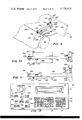
- FIG. 1 is a perspective view of the present optical web inspection system
- FIG. 2 is a block diagram of the basic components of the system shown in FIG. 1;
- FIG. 3 is an end-sectional view of the web inspection system head assembly of the present invention shown in FIG. 1;
- FIG. 4 is a front view, partially broken away, of the web inspection system head assembly shown in FIG. 1;
- FIG. 5 is a top plan view, partially broken away, of the web inspection system head assembly shown in FIG. 4;
- FIG. 6 is an enlarged perspective view of the web inspection system head assembly with the baffle in a raised position to view the inspection area;
- FIG. 7 is a side elevation view, in section, of a camera assembly of the web inspection system head
- FIG. 8 is a sectional view taken generally along sectional lines 8--8 of FIG. 7 of the camera assembly of the web inspection system head;
- FIG. 9 is an enlarged perspective view of the seam detector of the present invention shown in FIG. 6;
- FIG. 10 is a top plan view of the seam detector shown in FIG. 9;
- FIG. 11 is a side elevation view of the seam detector shown in FIG. 9;
- FIG. 12 is a top plan view of the yardage encoder assembly shown in FIG. 6;
- FIG. 13 is an end view of the yardage encoder assembly shown in FIG. 12;
- FIG. 14 is a side elevation view of the yardage encoder assembly shown in FIG. 12;
- FIG. 15 is a front view of the control panel of the web inspection system shown in FIG. 1;
- FIG. 16 is a block diagram of the basic electrical circuitry of the present web inspection system.
- FIG. 17 is a block diagram of the control and timing circuitry shown in block diagram of FIG. 16;
- FIG. 18 is a block diagram of the memory and arithmetic function circuitry shown in block diagram of FIG. 16;
- FIG. 19A is a detailed block diagram of the scan assembly memory of the memory circuitry shown in block diagram of FIG. 18;
- FIG. 19B is a block diagram of the sensor head circuitry shown in block diagram of FIG. 16;
- FIG. 20 is a detailed block diagram of the scan memory circuitry of the memory circuitry shown in block diagram of FIG. 18;
- FIG. 21 is a detailed block diagram of the area sum arithmetic function circuitry shown in block diagram of FIG. 18;
- FIG. 22 is an illustration of a transverse portion of a web, showing the scan of the web and the motion of the area sum matrix
- FIG. 23 is an illustration of the successive transverse portions of a web and the discrete segments within the transverse portions of the area sum matrix utilized to calculate the area sum;
- FIG. 24 is a detailed block diagram of the defect detection, data and width circuitry shown in block diagram of FIG. 18;
- FIG. 25 is an illustration of the defect cell configurations resulting in a defect determination
- FIG. 26 is a detailed block diagram of the velocity correction circuitry shown in block diagram of FIG. 17;
- FIG. 27 is a detailed schematic diagram of the scan assembly memory shown in block diagram in FIG. 18;
- FIG. 28 is a detailed schematic diagram of a portion of the scan memory circuitry shown in block diagram in FIG. 20;
- FIG. 29 is a detailed schematic diagram of a portion of the scan memory circuitry and the test cell delay memory circuitry shown in block diagram in FIG. 20;
- FIG. 30 is a detailed schematic diagram of the stack memory and a portion of the arithmetic function circuitry shown in block diagram in FIG. 18;
- FIG. 31 is a detailed schematic diagram of the offset selector circuitry of the scan memory circuitry shown in block diagram in FIG. 18;
- FIG. 32 is a detailed schematic diagram of a portion of the arithmetic function circuitry shown in block diagram in FIG. 18;
- FIG. 33 is a detailed schematic diagram of the data compaction circuitry of the scan memory circuitry shown in block diagram in FIG. 24;
- FIG. 34 is a detailed schematic diagram of the width circuitry shown in block diagram of FIG. 24;
- FIGS. 35A and 35B are detailed schematic diagrams of a portion of the computer interface circuitry shown in block diagram of FIG. 16;
- FIG. 36 is a detailed schematic diagram of a portion of the computer interface circuitry shown in block diagram of FIG. 16;
- FIG. 37 is a detailed schematic diagram of a portion of the control and timing circuitry shown in block diagram of FIG. 16;
- FIG. 38 is a detailed schematic diagram of the velocity correction circuitry shown in block diagram of FIG. 26;
- FIG. 39 is a detailed schematic diagram of a portion of the control panel display circuitry
- FIG. 40 is a detailed schematic diagram of the control panel keyboard circuitry.
- FIG. 41 is a detailed schematic diagram of a portion of the control panel display circuitry.
- the web inspection system includes an inspection head assembly identified generally by the numeral 50.
- the inspection head assembly 50 is mounted on an inspection housing 52 for an off-line inspection operation.
- the inspection head assembly 50 is interconnected to an electronic console unit 54 through interconnecting cables 56 and 58.
- the electronic console unit 54 includes a digital computer 60 and a preprocessor 62.
- a control panel 64 is provided to allow an operator to enter data into the computer 60.
- the control panel 64 includes an alphanumeric display 66, functionalized keyboards 68 and 69 and status lights identified generally by the numeral 70.
- Storage memory for the comuter 60 is provided by a magnetic disc assembly 72, which is also contained within the electronic console unit 54.
- a printer 74 is interconnected to the computer 60 to provide an output report of the defects detected during the inspection process.
- the fabric handler system for a stand-alone batch processor includes an A-frame support 76 positioned to the rear of the fbric inspection housing 52.
- Support 76 rotatably supports a roll of fabric 78 to be inspected.
- a motor 80 contained within the A-frame support 76 drives a fabric web 77 from the roll 78 upwardly over a roller 82 to a roller 84 mounted at the top of the inspection housing 52.
- a cylinder 85 is utilized to support the roller 82 on the inspection housing 52.
- a second drive motor 86, mounted within the inspection housing 52, ensures that the fabric web 77 moves uniformly across the inspection housing prior to the fabric web 77 being drawn through the inspection head assembly 50.
- a batcher 90 serves as a take-up device that actually re-rolls the fabric web once inspected.
- a drive motor 92 is mounted on the batcher 90 to re-roll the fabric on a roll 94.
- the batcher 90 also provides an automatic edge guide to re-roll the inspected fabric guided to one end of the batcher 90.
- the path of the fabric through the inspection head assembly 50 and inspection housing 52 conforms to the direction of arrows 96 from the uninspected roll of fabric 78, arrow 98 towards the top of the inspection table 52 and arrow 100 as the fabric web 77 leaves the inspection head assembly 50 to the batcher 90.
- the inspection head assembly 50 can be mounted on a frame located at the end of a production line prior to the batching operation. In this in-line mode of operation, the motivating force for pulling the fabric through the head is provided by the in-line batcher.
- FIG. 2 illustrates a block diagram of the interconnection of the basic components of the present system.
- the fabric handler 102 varies depending upon whether batch or in-line inspection is to be performed.
- the fabric take-up devices provide the force to drive the fabric web 77 through the inspection head 50.
- the inspection head 50 includes a plurality of self-scanning photosensitive detectors. These detectors electronically visually view the surface of the fabric to be inspected and convert the fabric surface into electrical information such that the fabric can be analyzed for flaws.
- the inspection head assembly 50 also includes an encoder assembly to produce electrical signals for measuring yardage and velocity information, the operation of which will subsequently be described.
- a mechanically actuated device for detecting seams in the fabric web 77 is also included within the inspection head assembly 50, which will also be subsequently described.
- the electrical data gathered by the optical detectors located within the inspection head assembly 50 is applied to the preprocessor 62, which accumulates the data and has an input into the computer 60.
- An important aspect of the present invention is the generation of a reference value corresponding to reflected radiation of a predetermined area or area matrix surrounding a discrete segment of the fabric web.
- the preprocessor 62 differentiates a detected defect from the normal background variations found in the fabric surface by comparing the reflected radiation of a discrete segment of the web with the reflected radiation from the area matrix.
- the preprocessor 62 also performs a data compaction function upon the defect data to reduce the work load of the computer 60.
- the preprocessor 62 also contains all timing generation circuitry for the inspection system and the logic circuitry for the yardage counter and velocity correction circuitry.
- the computer 60 provides the defect grading function according to any of the standard fabric grading rules adopted by the textile industry.
- the computer 60 receives the defect data from the preprocessor 62 and assigns the grading points to that defect based upon its length, in either the warp or the fill directions.
- the number of points assigned to the defect is under software control.
- the computer 60 then generates an output defect report detailing the type and location of a particular defect.
- the output report is printed by the printer 74.
- the input-output devices identified generally by the numeral 104 in FIG. 2 include the printer 74, the operator controls located on the control panel 64 and the disc assembly 72.
- the operator through the keyboards 68 and 69 can enter general information concerning the roll of fabric, such as style, loom number and bale number.
- the operator can also start or stop the inspection process through the control panel 64.
- the disc system 72 provides software initialization at the beginning of an inspection cycle as well as provides overflow capacity for defect reports if the printer 74 is over loaded.
- the disc system 72 may also be utilized to accumulate information used by another computer to analyze the defect data.
- the output device in addition to including a printer, could also include a computer to perform additional analysis on the data or a graphic display terminal to display a visual map of the fabric defects.
- the computer 60 comprises a general purpose digital computer such as a Hewlett Packard 2105MX series manufactured and sold by Hewlett Packard of Palo Alto, Calif.
- a Hewlett Packard 2105MX series manufactured and sold by Hewlett Packard of Palo Alto, Calif.
- the disc system 72 may comprise, for example, a Sykes Model 7250 system manufactured and sold by the Sykes Corporation.
- the printer 74 comprises a Centronics Model 588 system manufactured and sold by the Centronics Data Computer Corporation of Hudson, New Hampshire.
- the Centronics Model 588 Reference Manual which is incorporated herein by reference.
- the alphanumeric display 66 may comprise any suitable self-scan display.
- the Burroughs Corporation Gas Discharge Display Model SSD0132-0040 manufactured and sold by the Burroughs Corporation, Plainfield, N.J. may be utilized with the present system.
- the keyboard 68 may comprise, for example, the keyboard Model PX1-2 manufactured and sold by Micro Switch of Freeport, Ill.
- the inspection head assembly 50 includes a plenum or light box 110.
- the plenum 110 is defined by a beam 112 at its upper end, a front cover 114 and a rear cover 116. Front cover 114 has been removed from the illustration of the inspection head assembly 50 in FIG. 1.
- the lower end of the plenum 110 is defined by a light baffle 118, which includes an aperture 120.
- the plenum 110 is pressurized by fans 122, which are mounted to the rear cover 116 of the plenum 110. Outside air is drawn into the plenum 110 by the fans 122 through a filter 124 mounted to a housing cover 126. The pressurized air flows from the fans 122 through an aperture 128 into the plenum 110. The pressurization of plenum 110 serves to prevent dirt and lint from entering or accumulating within the inspection head assembly 50. Aperture 120 in the light baffle 118 provides a controlled orifice for the air inside the plenum 110 to escape.
- the plenum 110 can be positively pressurized to a pressure sufficient to keep dirt and lint from entering the plenum 110, while not distorting the fabric web 77 as it moves through the inspection head assembly 50.
- an imager assembly generally identified by the numeral 132, which will subsequently be described.
- the fabric web 77 is positioned within the inspection head assembly 50 using four fabric rollers 134, 136, 138 and 140.
- the fabric rollers 134, 136, 138 and 140 are not powered within the inspection head assembly 50 but are free running. Rollers 134, 136, 138 and 140 introduce sufficient friction to the flow of the fabric web 77 to ensure that the fabric web 77 lies flat and is maintained within the object space or inspection area identified by the numeral 142.
- Fabric rollers 136 and 138 maintain the surface of the fabric web 77 flat and uniform to prevent any wrinkles from occurring as the fabric web 77 moves through the object space 142.
- Fabric rollers 134 and 140 ensure that the fabric web 77 is maintained tightly against rollers 136 and 138.
- the fabric web 77 as it is pulled through the inspection head assembly 50 by an on-line or off-line batcher travels under fabric roller 140, above fabric rollers 138 and 136 and finally under fabric roller 134.
- Fabric roller 136 also functions as a planar reference surface for a yardage encoder assembly generally identified by the numeral 144.
- the yardage encoder 144 is an electrical encoder utilized to measure the length of the fabric web 77 as it passes through the inspection head assembly 50.
- the yardage encoder 144 also serves to generate an output signal that is used to derive the basic timing signals for the inspection system, which correct for velocity changes in the fabric web 77 as it passes through the inspection head assembly 50.
- the velocity correction signals generated by the yardage encoder 144 provide an input to the preprocessor 62 to correct for velocity changes in the fabric web 77 in the processing of the data produced by the imager assembly 132.
- Fabric roller 138 provides a planar reference surface for a mechanical seam detector identified generally by the numeral 146. Although a seam in the fabric web 77 will be detected optically by the imager assembly 132, it is also necessary to detect seams mechanically to distinguish between an actual seam and a defect which extends across the fabric web 77. The operation of the seam detector 146 will be subsequently described in connection with FIGS. 9, 10 and 11.
- the illumination source for the imager assembly 132 is provided by a fluorescent lamp 150 positioned below the light baffle 118 and transverse to the direction of the moving fabric web 77.
- the fluorescent lamp 150 is mounted within the inspection head assembly 50 using a bracket 152.
- the baffle 118 provides a light shield from the direct rays of the fluorescent lamp 150 from reflecting upwardly to the imager assembly 132.
- the fluorescent lamp 150 is 96 inches long to provide a uniform source of illumination within the inspection area 142 to incident on the fabric web 77.
- Other uniform light sources may be substituted for the fluorescent lamp 150.
- a tungsten light source employing filters to eliminate the infrared component of the light may be utilized.
- the fluorescent lamp 150 operates from a direct current source to eliminate the 60 Hz flicker present in fluorescent lamps.
- the imager assembly 132 includes an array of cameras or sensors, identified individually by the numeral 160.
- twelve such cameras 160 extend transversely across the inspection head assembly 50.
- a smaller number of cameras can be utilized having an enlarged field of view.
- Each camera 160 views a 6.4 inch section of the total field of view within the inspection area 142.
- the total field of view therefore, is 76.8 inches, which allows for a 4.8 inch over-scan on a typical fabric web having a width of 72 inches.
- Each camera 160 includes a photosensitive detector, which in the preferred embodiment, contains 64 elements. Therefore, utilizing a total of twelve cameras, each having a 64 element detector, there are present a total of 768 detector elements in the imager assembly 132. Each of the 768 detector elements thus views a 0.1 inch segment across the 76.8 inch inspection area transversing the fabric web 77.
- the fabric web 77 is viewed by the imager assembly as a 0.1 inch wide strip transversing the width of the fabric web 77. This strip or transverse portion of the fabric web 77 is segmented by the detector elements into 768 equally-spaced discrete segments.
- An alternative to the use of twelve cameras 160 each including a 64 element photosensitive detector would be to utilize three cameras 160 each employing a photosensitive detector having 256 elements.
- a short focal length lens of from 10-13 millimeters is utilized in each of the cameras 160.
- This focal length in combination with the 0.1 inch resolution per detector element provides a visual acuity similar to that of a human inspector viewing the inspection area from a distance of about 3.5 feet.
- the system therefore, is capable of detecting flaws in the fabric web 77 which a human operator would detect.
- the fabric inspection system utilizing these parameters is designed not to identify defects that a human operator would not or that are very difficult for the human operator to see.
- Each rack assembly 162 contains a printed circuit board containing the amplifiers and analog to digital converters associated with each of the cameras 160 in the four camera group. Also included in the circuitry contained by the rack 162 is a 4 to 1 multiplexer which sequences through the four cameras within each group.
- fans 122 serve to pressurize the plenum 110.
- Fans 122 also serve to circulate air within the imager assembly 132 to cool the electronic components housed within the rack assemblies 162.
- the inspection head assembly 50 is illustrated.
- the front plenum cover 114 has been removed and the light baffle 118 has been raised from its normal position as shown in FIGS. 1 and 3.
- the direction of the movement of fabric web 77 through the inspection head assembly 50 is indicated by the arrow 170.
- Cameras 160 are enclosed by the housing cover 126 at the top of the inspection head assembly 50. The cameras 160 are mounted to the beam 112 and receive the reflected radiation from the surface of fabric web 77 in the object space 142 through aperture 120 and lens apertures 172 contained within the beam 112.
- Each camera 160 includes a self-scanning photosensitive detector 180, such as a solid state line scanner Model RL-64P manufactured and sold by Reticon Corporation of Mountainview, Calif. Alternatively, charge couples, charge injection, or bucket brigade devices may be utilized as detectors.
- the detector 180 is glued to a positioning plate 182.
- Positioning plate 182 is adjustable within a guide plate 183 in the direction indicated by the arrows labeled "Y" by setting screws 184.
- a second positioning plate 186 adjustable within a guide plate 187 permits the detector 180 to be positioned in the direction of arrows labeled "X" through the adjustment of screws 188.
- a third positioning plate 190 allows the detector 180 to be rotated in the direction indicated by the arrows labeled " ⁇ " by adjusting screws 192. Through the adjustment of plates 182, 186 and 190, the detector 180 can be properly positioned within each camera 160.
- Focus of the camera lens 196 is accomplished by turning the focus ring 198.
- a number of lenses may be utilized in conjunction with the present camera. However, in the preferred embodiment of the invention, the lens utilized has a focalling of 12.5 millimeters and is lens Model 87022 manufactured and sold by Cosmicar Optical Company of Tokyo, Japan.
- the 16 pins 200 of detector 180 are plugged into a socket 202, which is interconnected to an extender cable 204 having plugs 206 and 208 at its ends.
- Plug 206 mates with socket 202
- plug 208 mates with a socket 210.
- Socket 210 is mounted to an amplifier printed circuit board 212, which is mounted by spacers 214 to a mounting plate 216.
- Mounting plate 216 is utilized to mount the camera 160 to the beam 112 (FIG. 6).
- the entire amplifier card 212, detector 180 and positioning plates 182, 186 and 190 are enclosed by a cover 218, which is positioned in a slot 220 within the mounting plate 216.
- a rubber O-ring 222 is positioned in the slot 220 to provide a gasket-type seal between the cover 218 and mounting plate 216.
- the cover 218 is mechanically attached to the mounting plate 216 using brackets 224 and screws 226.
- Positioning and alignment of the sensor 180 is accomplished using an alignment fixture. Alignment of each camera is accomplished on an optical bench using reference pin holes which are identical to the pin holes located on the beam 112 (FIG. 6). Each camera 160 can therefore be independently aligned prior to being installed within the inspection head assembly 50 without the field of views of each camera overlapping.
- the mechanical seam detector assembly 146 is illustrated.
- the seam detector 146 is mounted within the inspection head assembly 50 to wall 250 (FIG. 3) using a mounting block 252.
- a clevis 254 is pivotally mounted to the block 252, and receives a first arm member 256.
- Mounted to the end of arm 256 is a bearing 258.
- the bearing 258 is constantly in contact with the fabric web 77 as the fabric web 77 moves across fabric roller 138 in the direction indicated by the arrow 260.
- Arm 256 is mounted to the clevis 254 using a pin 262 and a torsion spring 264.
- a second arm member 266 is pivotally mounted using a pin 268 to arm member 256.
- a rod 270 mounted to the end of arm 266 is a rod 270, which includes bearing 272.
- Bearings 272 are smaller in diameter than the bearing 258. Due to the relative position of arms 256 and 266, bearings 272 contact a portion of the fabric web 77 prior to the contact of the same portion of fabric web 77 with the bearing 258. Bearings 272 are always in contact with the fabric web 77 as the web 77 moves across the fabric roller 138.
- a micro switch 274 is mounted on the arm member 256 and has a normally open contact 276. Because arm member 266 is free to move independently of arm member 256, the arms 256 and 266 act as a fabric thickness differentiator. As a fabric seam 280 (FIG. 9) approaches the mechanical seam detector 146, the seam will contact the bearing 272 mounted on arm 266 and cause arm 266 to be pivoted upwardly. This upward motion towards arm member 256 will cause a contact 282 mounted on arm member 266 to engage contact 276 of the micro switch 274, which will then generate an electrical signal indicating that a change in thickness of the fabric web 77 has been detected. This change in thickness is caused by the passage of the fabric seam 280 under bearings 272.
- Arm members 256 and 266 measure the relative difference between the thickness of the fabric web 77 as the web 77 contacts the bearing 258 as compared to the thickness of the web 77 where it contacts the bearings 272.
- the detection of a seam is, therefore, accomplished by measuring the relative differences in the fabric web thickness as a point on the fabric moves across the bearings 272 and 258. This measurement avoids the necessity of making a precise thickness determination and comparisons to that initial measurement.
- a shaft 284 mounted through the clevis 254 and mounting block 252 is a shaft 284 on which a block 286 is mounted.
- Block 286 includes an aperture 287, which permits the shaft 284 to move vertically up and down through the block 286.
- a compression spring 288 is mounted around shaft 284 between the clevis 254 and the block 286. The rod 284, block 286 and compression spring 288 permit the mechanical seam detector 146 to be rotated to a position parallel to the wall 250 of the inspection head assembly 50 such that the seam detector assembly 146 will be disengaged from the fabric roller 138. This disengagement permits easy threading of the fabric web 77 through the inspection head assembly 50 prior to beginning the inspection process.
- the positioning process is accomplished by raising arm member 256 such that the clevis 254 contacts the block 286 thereby compressing the spring 288.
- the arm member 256 is then rotated to a position parallel to wall 250 to cause a pin 290 mounted to the shaft 284 to engage the upper surface of the block 286, thereby maintaining the spring 288 in its compressed state.
- the encoder assembly 144 includes an optical encoder 300.
- a number of encoders may be utilized in conjunction with the present system.
- the encoder 300 may comprise, for example, a Model 30-HDE-600 encoder manufactured and sold by Renco Corporation of Golet, Calif.
- Power is supplied to the encoder 300 through a plug 302.
- An arm 304 is rigidly attached to the encoder 300, and is mounted through a shaft 306 to a mounting bracket 308.
- Mounting bracket 308 is mounted to a rail 310 (FIG. 3) which extends across the length of the fabric inspection head assembly 50.
- An encoder wheel 312 is mounted on an encoder shaft 314.
- the encoder wheel 312 contacts the fabric web 77 as the fabric web 77 moves across the fabric roller 136 (FIG. 3).
- the encoder wheel 312 constantly engages the fabric web 77 as it passes over the roller 136 through the use of a torsion spring 316.
- Torsion spring 316 causes the arm 304 to apply sufficient pressure to the encoder wheel 312 to maintain contact with the fabric web 77.
- the output of the encoder 300 generates 600 pulses per revolution of the encoder shaft.
- the circumference of the encoder wheel 312 is one foot, such that the encoder generates 600 pulses per revolution or 600 pulses per one foot of fabric passing under the encoder wheel 312.
- the output of the encoder 300 is then applied to the control and timing circuitry of the preprocessor 62 to be subsequently described.
- the control panel 64 of the fabric inspection system of the present invention includes a self-scan panel display 66, alpha key set 68 and a numeric key set 69.
- the operator first depresses the key 320 labeled "ENTER.”
- the display 66 will then request the operator to supply a fabric bale identification number.
- the operator will then enter through the key set 69 a bale number, which can have a maximum of 10 digits.
- the operator will then depress key 322 labeled "NEXT,” which will cause the display 66 to request the operator to supply a fabric loom number.
- the loom number can be any number up to 32,000.
- the operator will then depress key 322, which will cause the display 66 to display a message inquiring as to the width of the fabric to be inspected.
- the operator then using key set 69 will enter the width of the fabric to be inspected and again depress the key 322.
- the display 66 will then display a message inquiring as to the style number of the fabric to be inspected.
- the operator will then enter through the key sets 68 and 69 an alpha/numeric designation to indicate the style.
- the operator will then depress key 322, and display 66 will indicate that the fabric bale number previously entered is being inspected.
- the printer 74 (FIG. 1) will begin to print the data entered by the operator, bale number, loom number, width and style on the defect output report.
- the inspection process will begin after the fabric web 77 has achieved the desired inspection velocity through the inspection head assembly 50.
- the diagnostic indicators and switches 70 include a "VELOCITY ERROR” indicator 324, which is illuminated if the velocity of the fabric web 77 is either too high or too low for proper inspection to take place.
- the "NO FABRIC” indicator 326 is illuminated if there is an absence of fabric within the inspection head assembly 50 during an inspection process.
- the "READY” indicator 328 is illuminated to indicate that the necessary information has been entered into the computer 60 and that the system is ready to begin the inspection process.
- a "FAULT” indicator 330 is illuminated to indicate that a problem exists in the system's hardware. A diagnostic error message will then be output from the computer 60 to the printer 74.
- a push button switch 322 identified as “SENSOR ON” is depressed to supply power for all of the electronics within the inspection head assembly 50.
- a push button switch 334 is depressed to supply power to the fluorescent lamp 150 and is labeled “LMP PWR.”
- a "LAMP START” push button switch 336 is depressed for approximately 10 seconds to energize the lamp 150.
- the "LPM ON" indicator 338 will be illuminated to indicate to the operator that the lamp 150 is actually on. Since the lamp 150 is totally enclosed within the inspection head assembly 50 the only indication the operator has as to whether the lamp is properly functioning is the indicator 338.
- Push button switches labeled "MAN RUN” 340 and “MAN STOP” 342 permit the operator to manually run or stop the inspection process.
- An indicator labeled "AUTO RUN” 344 will be illuminated when the operator has depressed key 322 after entering the style information through the key set 69. The illumination of indicator 344 will indicate that the system is inspecting fabric.
- An indicator labeled "AUTO STOP” 346 is illuminated when the system has detected a hardware fault and will automatically discontinue fabric inspection.
- An emergency stop switch 348 when depressed will disconnect all power from the inspection head assembly 50 and the electronics console 54 (FIG. 1).
- the operator can enter through the control panel key sets 68 and 69 updated fabric information relative to a new piece or style of fabric which will subsequently be inspected.
- the computer 60 will cause the printer 74 to print out this new fabric identification information.
- the control and timing circuitry 360 includes a basic oscillator to generate all of the clock and strobe timing signals for the inspection head detectors and their associated circuitry 362, the preprocessor memory circuitry 364, the preprocessor arithmetic function circuitry 366 and the interface circuitry 368 to the computer 60 (FIG. 1).
- the fabric inspection head assembly 50 consisting of the twelve cameras 160 (FIGS. 4 and 5), for purposes of further discussion these twelve cameras are considered to be associated in three groups. Each camera group, therefore, consists of four cameras. An associated amplifier and analog to digital converter is associated with each of the twelve cameras.
- the control and timing circuitry 360 causes the three camera groups to be simultaneously scanned while at the same time successively scanning the four cameras within each group.
- each camera includes a 64 element detector such that a total of 768 detectors span across the width of the fabric web 77.
- Each of the 768 detectors view a one-tenth inch square segment of the fabric web during one complete scan of the 768 detectors.
- the term "cell” or "discrete segment” will represent one of the one-tenth inch square segments viewed by one of the elements of the 64 element camera detector.
- the first four cameras, group 1, located on the left side of the inspection head assembly 50 will scan detectors 1-256, the middle four cameras, group 2, will scan detectors 257-512 and the third group of four cameras located on the right side of the inspection head assembly 50 will scan detectors 513-768.
- the control and timing circuitry 360 will cause the inspection head detectors and associated circuitry 362 to output data to the memory circuitry 364 in the form of three parallel sets of data, one set from each of the camera groups. These three sets of parallel data comprise the outputs of the cameras of group 1 representing cells 1-256, the output of the cameras of group 2 representing cells 257-512, and the output of the cameras of group 3 representing cells 513-768.
- the memory circuitry 364 also receives clock and strobe timing signals from the control and timing circuitry 360.
- the memory circuitry 364 reconstructs the three sets of parallel input data from the inspection head detectors 362 to a serial representation of the data. This serial reconstruction of the data to represent the output of the three groups of cameras in sequential order from cell 1 to cell 768 is accomplished in a scan assembly memory portion of the memory circuitry 364.
- the output of the scan assembly memory represents the output data of the cameras 160 in serial form representing a complete scan of the 768 cells across the width of the fabric web 77.
- Each scan represents the output of the detectors measuring the reflected radiation from a transverse portion of the fabric web 77 measuring one-tenth inch in length across the width of the web 77.
- the output of the scan assembly memory is applied to a scan memory portion of the memory circuitry 364, which stores a total of eight scans of data representing the output of the twelve cameras during eight transversals of the fabric web 77.
- the data from the eight sequential scans of the fabric web 77 is stored in the scan memory portion of memory circuitry 364 with access to that data at 1536 cell intervals. New data is continually shifted into the scan memory, pushing out previously stored data to create a rolling memory, which is continuously changing as new scans of data are added to the memory circuitry 364.
- the storage of eight sequential scans of the fabric web 77 create parallel access to five cells corresponding to the same cell location in each of the eight sequential scans.
- the combination of the same cell location for sequential scans for purposes of discussion will be termed a "row" of cells.
- the output values of the five cells constituting a row are parallel input into a stack memory of the memory circuitry 364 for input into the arithmetic function circuitry 366.
- the output data of three contiguous cells located in a single scan are tapped off and input parallel into the stack memory for storage.
- the three contiguous cells are termed "test" cells.
- the five cells from a row and the three test cells stored in the stack memory is then output serially to the arithmetic function circuitry 366.
- the arithmetic function circuitry 366 includes circuitry to generate the area of matrix sum which represents the sum of the value of the five cells stored in the stack memory plus four additional row sums to constitute the data from 25 different cells. This calculation of an area sum for the value of 25 cells is calculated each time a complete scan of the 768 elements across the fabric web 77 is made by the twelve cameras 160. The sum of the 25 cells creates a moving low resolution field representing the normal background variations of the fabric web 77 over the particular rows and scans which constitute the area from which the 25 cells are selected.
- the output values of the three test cells selected from within the area utilized to calculate the area sum are each compared to the area sum. Through this comparison of a single test cell to the area sum of 25 cells, the determination of whether the test cell represents a defect present within the fabric web 77 is made. If the test cell value is greater or less than the area sum value by more than a predetermined amount for the particular fabric being inspected a defect signal is generated and applied to the data compaction circuitry within the arithmetic function circuitry 366.
- the defect data is applied to the computer interface 368, which correlates the particular defect with the yard at which the defect occurred along the fabric web 77.
- the computer interface 368 compensates for any changes in velocity of the fabric web as it moves through the fabric inspection head assembly 50 utilizing the clock and strobe timing signals generated by the control and timing circuitry 360.
- the location and defect information is then output from the computer interface 368 to the computer 60 for the assignment of grading points to the particular defect and for preparation of the output report analysis.
- FIG. 17 a block diagram of the control and timing circuitry 360 (FIG. 16) is illustrated.
- An oscillator 380 having a frequency of 6.912 MHz supplies an output to a counter 382.
- Counter 382 performs a divide by 30 function to generate a timing signal for each cell time.
- the output of counter 382 is applied to a read only memory 384 to generate clock timing signals CLK1, CLK2, CLK7 and CLK14.
- Clocking signal CLK7 is utilized to clock the cameras 160.
- Clocking signal CLK14 is utilized to clock the analog to digital converters associated with each camera 160 and the clocking signals CLK1 and CLK2 are utilized to clock various functions within the scan assembly memory of the memory circuitry 364.
- the output of counter 382 is also applied to a counter 386.
- Counter 386 performs a divide by 256 function to generate timing pulses for each of the 256 cells within each of the three camera groups.
- the output of counter 386 is applied to read only memories 388 and 390.
- the output of read only memory 388 generates the S10 and S11 timing signals, which are applied to the multiplexer associated with each group of cameras 160.
- Read only memory 390 generates the S1, S2, S3 and S4 timing signals, which provide the start pulses for each camera 160.
- the outputs of read only memories 384, 388 and 390 provide all of the timing pulses for the cameras 160 and imager assembly 132 circuitry contained within the fabric inspection head assembly 50.
- the scan rate of the number of pulses generated or needed to transverse the full 768 cells across the fabric web 77 is maintained constant regardless of changes in the velocity of the fabric web as it moves through the inspection head assembly 50.
- the scan rate is approximately 1.1 milliseconds. This rate would equate to approximately 10 scans per linear inch of fabric having a velocity of 150 yards per minute. Compensation for changes in velocity of the fabric web is controlled by the timing pulses supplied to the memory circuitry 364, arithmetic function circuitry 366 and computer interface circuitry 368 (FIG. 16).
- an adjustment in the number of scans of data supplied to the memory circuitry is made. If the velocity increases above a predetermined amount, certain ones of the scans are accumulated to compensate for lost data. Should the velocity of the fabric web decrease below a specified value, the number of scans per linear inch of fabric will increase and it will be necessary to disregard or skip scans before the data is entered into the memory circuitry 364. Correction for velocity of the fabric web by ignoring some scans or adding scans is utilized as an alternative to changing the exposure time the cameras 160 view a portion of the fabric web.
- the exposure time is maintained constant, there is a constant scan interval maintained by the cameras, there is a constant iris opening on the lens of each camera and there is a constant light output from the radiation source.
- the velocity correction circuitry includes the yardage encoder assembly 144, which generates an output of 600 pulses per foot for application to a counter 392 (FIG. 17).
- Counter 392 performs a divide by five function and has its output applied to a counter 394.
- Counter 394 provides a divide by ten function to generate an output pulse representing one pulse per inch.
- the one pulse per inch output of counter 394 is applied to a counter 396 which counts the number of inches of the fabric web passing through the inspection head assembly 50.
- the output of counter 396 is applied to the computer interface 368 (FIG. 16) and to a counter 398.
- Counter 398 counts the number of yards of fabric which have passed through the fabric inspection head assembly 50 and provides an output to the computer interface 368 indicating yardage information.
- the output of counter 394 representing one pulse per inch is applied to a counter 400, which also receives the output of counter 386.
- the output of counter 386 represents the number of scans, while the output of counter 394 represents pulses per inch.
- Counter 400 therefore counts actual scans per inch.
- the output of counter 400 is applied to read only memories 402 and 404.
- Read only memories 402 and 404 generate a velocity correction code, which is dependent upon the output of counter 400.
- the velocity correction code is a number having a value from one to seven, in which one indicates no correction is necessary and seven indicates a maximum correction is required.
- the velocity correction code is then held in a latch 406 and applied to a counter 408.
- Counter 408 Applied to counter 408 is the basic oscillator frequency from the oscillator 380.
- Counter 408 performs a division of the basic oscillator frequency, dividing by the number, one through seven, generated by the read only memories 402 and 404 representing the velocity correction code.
- the output of counter 408 is applied to a counter 410, which performs a divide by thirty function to generate an output which represents corrected cell time.
- the output of counter 410 is an output equivalent to that of the counter 382 but corrected by the velocity correction code to compensate for changes in the velocity of the fabric web 77.
- the output of counter 410 is applied to read only memories 412 and 414, which generate all of the timing pulses for the memory circuitry 364, arithmetic function circuitry 366 and computer interface circuitry 368 (FIG. 16).
- Read only memory 412 generates the CLK3, 4, 5, 9, 10, 11 and 12 timing signals.
- Read only memory 414 generates the S5, 6, 7 and 8 timing signals.
- the output of counter 410 is also applied to a counter 416.
- Counter 416 provides a divide by 256 function to provide an output that represents cell time per scan similar to the function of counter 386 but which has been corrected by the velocity correction code.
- the output of counter 416 is applied to a counter 418 together with the velocity correction code generated by read only memories 402 and 404.
- the output of counter 418, the S15 timing signal is applied to the data compaction circuitry, whose function will be subsequently described.
- the output of counter 416 is also applied to a counter 420, whose output, the S16 timing signal, is applied to the width circuitry.
- the memory circuitry 364 and arithmetic function circuitry 366 are illustrated in block diagram.
- the outputs of the four cameras within camera group 1 representing the outputs of the camera detectors corresponding to cells 1-256 are applied to a multiplexer 422.
- the outputs of the four cameras comprising the camera group 2 are applied to a multiplexer 424.
- the outputs of the four cameras comprising camera group 3 are applied to a multiplexer 426.
- the output of the inspection head detector circuitry 362 (FIG. 16) is in the form of three parallel inputs of eight bits each to the three multiplexers 422, 424, and 426.
- the multiplexers 422, 424 and 426 are 2 to 1 multiplexers that determine whether the scan data is applied to a scan assembly memory 428 or a scan assembly memory 430.
- the input data to either scan assembly memory 428 or 430 is in the form of three input parallel while the output of the scan assembly memories 428 and 430 is one output serial.
- the scan assembly memories 428 and 430 assemble the scans from the three parallel inputs representing cells 1-256, 257-512, and 513-768 into a continuous scan of cells 1-768. Because the scan assembly memories 428 and 430 are assembling the three input parallel data to a single serial output, the data must be shifted out of scan assembly memories 428 and 430 at a rate of three times the parallel input rate.
- the mulitplexers 422, 424, and 426 alternately supply inputs to either scan assembly memory 428 or scan assembly memory 430.
- scan assembly memory 428 or 430 When either scan assembly memory 428 or 430 is receiving data, the other is serially unloading data to a multiplexer 432.
- Scan assembly memories 428 and 430 therefore, alternate functions; as one is receiving data, the other scan assembly memory is transferring a serial output to the scan memory circuitry of the memory circuitry 364 (FIG. 16).
- the operation of the scan assembly memories 428 and 430 will be further described in conjunction with FIG. 19A.
- the output of multiplexer 432 (FIG. 18) is applied to a scan memory identified generally by the numeral 434.
- the scan memory 434 comprises forty-eight 1024, bit shift registers 435-482. Each of the shift registers 435-482 store 256 words by 4 bits per word. Data from eight sequential scans of the fabric web 77 is stored in the scan memory 434, such that the data from 6144 cells (eight scans times 768 cells per scan) are stored within the scan memory 434. Access to the data stored within scan memory 434 is accessed at 1536 cell intervals. For example, the interval between the cell data stored in shift register 435 and that stored in shift register 441 is 1536 cells. New data is continually shifted into the scan memory 434, which shifts out one scan of data during each scan of the twelve cameras 160.
- the same cell within five scans or a row of cells is tapped off from the scan memory 434 to a stack memory 484.
- the stack memory 484 comprises eight, 8 bit parallel in/serial out shift registers.
- one cell located within the fifth scan is tapped off from shift register 446 of the scan memory 434 and stored in shift registers 486-493.
- Shift registers 486-493 are 8 bit serial in/parallel out shift registers and comprise the test cell delay memory.
- the outputs of shift registers 491, 492 and 493 are applied to three inputs of each of the eight shift registers within stack memory 484.
- the cell data contained in shift registers 491, 492 and 493 comprises the data from three cells, which represent the test cells to be compared with the area sum or reference value.
- the reference value is calculated from summing the detector outputs corresponding to twenty-five cells located in a matrix having the center of the matrix as the test cell. The test cell selected and those cells selected for the calculation of the area sum value will be subsequently described in connection with the illustrations of FIGS. 22 and 23, and the block diagram of FIG. 20.
- the output of the stack memory 484 is applied to the arithmetic function circuitry 366 (FIG. 16).
- the five cell values stored in the stack memory 484 representing the same cell location in five scans of data stored in scan memory 434 are applied individually to an adder 496.
- the output of adder 496 is applied to an accumulator 498.
- Adder 496 and accumulator 498 are initially cleared to have a content of zero.
- the output of the accumulator 498 is also applied to the adder 496, which generates a sum of the contents of the accumulator 498 and each of the five cell values applied from stack memory 484.
- the adder 496 and accumulator 498 operate to generate a sum of the five cells stored in the stack memory 484. These five cells represent a row in the area sum matrix. Briefly, the summation operation is performed as follows:
- Step 1 Adder 496 and accumulator 498 are cleared.
- Step 2 Cell value 1 is shifted to adder 496 and summed with the contents of accumulator 498, zero, and shifted into accumulator 498.
- Step 3 Cell value 2 is shifted into adder 496 and summed with the contents of accumulator 498 (cell 1) and the summation value of cell 1 plus cell 2 is shifted into the accumulator 498.
- Step 4 Cell value 3 is shifted into adder 496 and summed with the contents of accumulator 498 (cell 1 plus cell 2) and the resultant sum is shifted to accumulator 498, which now contains the summation of cells 1, 2 and 3.
- Step 5 Cell value 4 is shifted into adder 496, and summed with the contents of accumulator 498 and shifted into accumulator 498. Accumulator 498 now contains the sum of cells 1, 2, 3 and 4.
- Column sum memory circuitry 500 includes eleven, 8 bit serial in/parallel out shift registers.
- the five values of the cells tapped off from the scan memory 434 and stored in stack memory 484 also continuously change.
- the summation operation formed by the adder 496 and accumulator 498 is performed six times to accumulate within the column sum memory circuitry 500 six individual sums. Each of these six individual sums represent the sum of a row of cells outputted from stack memory 484.
- the output of the column sum memory 500 is applied to an adder 502 and is applied through an inverter 504 to an adder 506.
- the output of adder 506 is applied to an accumulator 508, whose output is applied to adder 502.
- the function of adders 502 and 506, together with accumulator 508, is to create a sum of five of the row sum values stored within the column sum memory 500, which represents a sum of 25 cells. Since the contents of the column sum memory 500 is continuously changing, after each scan the oldest value stored within the memory 500 is subtracted through the inverter 504 by adder 506. The matrix sum of 25 cells is therefore continuously changing as new data is inputted into the column sum memory 500. The effect of this change in the cells which make up the 25 cells within the area sum matrix is illustrated in FIG. 22. The apparent motion of the area sum matrix is to progress from one edge of the fabric web 77 to the opposite edge of the fabric web.
- the area sum matrix is illustrated and identified by the numeral 510.
- the dimensions of the area sum matrix 510 is thirteen cells or rows long and nine cells wide.
- the total number of cells, 768, is also illustrated in FIG. 22 as transversing across the fabric web 77.
- the direction of the fabric web motion is indicated by the arrow 512, and the direction of the scan of the twelve cameras 160 is indicated by the arrow 514.
- the three test cell values stored in the stack memory 484 are applied individually to read only memories (ROMs) 520, 522 and 524.
- Read only memories 520, 522 and 524 are programmable ROMs and function to multiply by 25 each of the test cell values.
- the test cell value can then be compared to the value of the area sum matrix to determine whether the test cell value is either greater or less than the value of the area sum matrix for the determination of whether a defect exists in the test cell.
- the read only memories 520, 522 and 524 each has an address location which is a binary value equivalent to 25 times the address to generate a value which is 25 times the test cell value applied to the read only memory. This output value is then applied to an adder 526.
- Adder 526 also receives a predetermined value supplied by the computer 60 through the computer interface 368 (FIG. 16) to latches 528 and 530 through a multiplexer 532.
- This predetermined value supplied by the computer software is referred to as "offset" and is dependent upon the style of the fabric being inspected.
- the library of the computer 60 stores both a positive value and a negative value for each type of value to be inspected. The purpose of the offset value is to in effect reduce the sensitivity of the detectors within the cameras 160 to ensure that the value of the test cell is not merely noise when compared with the value of the area sum matrix.
- the adder 526 performs an addition function to add the output value from the read only memories 520, 522 and 524 to the offset value selected through multiplexer 532.
- the output of adder 526 is then applied to a comparator 536, which also receives the output of accumulator 508 representing the sum of the 25 cells within the area sum matrix.
- the output of the comparator 536 indicates that the test cell value is either greater than or less than the value of the area sum matrix.
- the output of comparator 536 is applied through a multiplexer 537 and a flip-flop 537a to a defect buffer 538.
- the defect buffer 538 stores the output of comparator 536 for comparisons between each of the three test cell values with the value of the area sum matrix for both positive and negative offset values.
- the output of the defect buffer 538 is applied to a defect configuration circuit 540.
- the defect configuration circuit 540 contains logic circuitry to determine whether the defects identified through the comparison made by comparator 536 and stored within the defect buffer 538 conform to one of the four defect configurations illustrated in FIG. 25.
- Configuration 1 represents defect cells 541 and 542 being contiguous cells from the same scan across the fabric web 77.
- Configuration 2 represents defect cells 543 and 544 being contiguous defect cells from different scans but of the same row.
- Defect configuration 3 represents defect cells 545 and 546 being contiguous cells of different scans and different rows.
- defect configuration 4 represents defect cells 547 and 548 being from different scans and different cells. If either of these four defect cells configurations is detected by the defect configuration circuit 540 (FIG. 18), the defect configuration circuit 540 applies an output to a defect latch 550.
- the defect latch 550 applies an output to the data compaction circuitry to be subsequently described.
- FIG. 19A a more detailed block diagram of the scan assembly memory circuitry 428 and 430 of FIG. 18 is illustrated.
- the outputs of the detectors comprising the four cameras of camera group 3 are alternately applied to multiplexer 426a of the scan assembly memory 428 and to multiplexer 426b of the scan assembly memory 430.
- the output of multiplexer 426a is applied to shift register 428a, which comprises two 4 ⁇ 256 bit shift registers.
- shift register 430a which comprises two 4 ⁇ 256 bit shift registers.
- the value of cells 513-768 are stored alternately within shift registers 428a and 430a.
- the output of the detectors of the cameras comprising camera group 2 are similarly applied to multiplexers 424a and 424b depending upon whether the scan assembly memory 428 is reading in or shifting out data.
- Multiplexers 424a and 424b are interconnected to shift registers 428b and 430b, which store the value of cells 257-512.
- the output of the detectors comprising the four cameras of camera group 1 are similarly applied to multiplexers 422a and 422b.
- Multiplexers 422a and 422b are interconnected to shift registers 428c and 430c.
- Shift registers 428c and 430c each comprise two, 4 ⁇ 256 bit shift registers, which store the values of cells 1-256.
- the outputs of shift registers 428c and 430c are alternately applied through the multiplexer 432 (FIG. 18) to the scan memory.
- FIG. 19B a more detailed block diagram of the inspection head detectors and circuitry 362 and its interconnection to the memory circuitry 364 (FIG. 16) is illustrated.
- the camera group 1 has been illustrated in FIG. 19B.
- the four cameras 160 of camera group 1 are individually interconnected to an associated amplifier 562, which is interconnected to an analog to digital converter 564.
- Amplifier 562a receives the S4 timing signal
- amplifier 562b receives the S3 timing signal
- amplifier 562c receives the S2 timing signal
- amplifier 562d receives the S1 amplifier signal.
- the CLK7 timing signal is applied to each of the amplifiers 562a-d and the analog to digital converters 564a-d.
- the output of the analog to digital converters 564a-d are applied to a multiplexer 566.
- Multiplexer 566 is a 4 to 1 multiplexer and receives the S10 and S11 timing signals.
- the amplifiers 562a-d, analog to digital converters 564a-d and multiplexer 566 are all contained on a printed circuit board housed within the rack assemblies 162 (FIG. 5) mounted within the inspection head assembly 50.
- multiplexer 566 The output of multiplexer 566 is applied to multiplexer 422 (FIG. 18) which receives the S9 timing signal.
- the output of multiplexer 422 is alternately applied to either of the scan assembly memories 428 or 430 (FIG. 19A).
- the selection of the proper timing signals for the scan assembly memories 428 and 430 are controlled by multiplexers 568 and 570 through inverters 572 and 574.
- Multiplexer 568 receives the CLK2, CLK4 and S2 timing signals.
- Multiplexer 570 receives the CLK1, CLK3 and S2 timing signals.
- Multiplexers 568 and 570 select the proper clock rate for loading and unloading the shift registers comprising the scan assembly memories 428 and 430.
- the output of the scan assembly memories 428 and 430 is applied through a multiplexer 432 to the scan memory 434.
- Each of the blocks 580-603 represents a 256 ⁇ 8 bit shift register which receives parallel data, outputs parallel data and stores 256 words by 8 bits per word. Each block 580-603 therefore, corresponds to two of the shift registers 435-482 of the scan memory 434 (FIG. 18).
- the scan memory 434 stores eight sequential scans of data of the fabric web 77 with access to that data at 1536 element intervals, correponding to cells 0, 1536, 3072, 4608 and 6144.
- the cell data from the output of multiplexer 432 (FIG. 18) is applied to the shift register block 580.
- the timing signals CLK3 and CLK4 are applied through inverters 604 and 605 to each of the shift register blocks 580-603.
- FIG. 23 illustrates an enlarged representation of a matrix 510 (FIG. 22) showing the individual cells of the matrix 510.
- the matrix 510 includes 13 horizontal rows, which are parallel to the fabric web motion indicated by arrow 512, and nine vertical columns which lie in the scan direction indicated by arrow 514.
- Row 1 of matrix 510 corresponds to the cell values in nine successive scans of the fabric web 77 and represents the first row of cells located at the fabric web edge 77a (FIG. 22).
- the cell values contained in columns 1, 3, 5, 7 and 9 of row 1 are tapped off from the scan memory 434 and stored in the stack memory 484 (FIG. 20).
- the three test cell values are also tapped from the scan memory 434 and stored within the stack memory 484.
- the values of the eight cells within column 5 of the matrix 510 are tapped off and stored in a test cell delay memory 610, which comprises the shift registers 486-493.
- the eight cell values of rows 1-8 of column 5 are serially input into shift registers 486-493.
- the three test cell values are then tapped from shift registers 491-493 and stored in the "TC" 1-3 shift register locations within the stack memory 484.
- Stack memory 484 comprises parallel in/serial out shift registers, such that on each scan of the fabric web 77 the value of the five cells from a row and the three test cell values are output serially from the stack memory 484 to the adder 496.
- the pattern of cells utilized in the calculation of the value of the area sum matrix illustrated in FIG. 23 is repeatedon alternate odd scans of the fabric web 77.
- the cells tapped off from the scan memory 434 are selected from the even columns of the matrix 510.
- the test cells selected are located centrally within the matrix 510. As the cell selection changes, to in effect cause the matrix 510 to move across the fabric web 77 from edge 77a to edge 77b in the direction of scan, the three test cell values also move across the width of the fabric web 77.
- every cell across the fabric web 77 will be selected as a test cell value and compared to the value of the 25 surrounding cells composing the area sum matrix. Not every cell is utilized in the calculation to form the area sum reference value.
- the area sum calculation cells illustrated in FIG. 23 in the 9 column by 13 row matrix 510 are utilized.
- various other patterns in the selection of the 25 area sum calculation cells can be utilized. The skipping of rows within the matrix from which the five column values are selected serves to improve the average value for the area sum matrix. Because the effective motion of the matrix 510 is across the fabric width, and because the fabric motion is normal to the motion of the matrix 510, a dynamic two dimensional matrix is formed from which the area sum value is calculated.
- the effective motion of the matrix 510 across the fabric web 77 from edge 77a to edge 77b is created through the operation of the column sum memory 500 (FIG. 18).
- the first value of the area sum matrix 510 as the matrix 510 moves across the fabric web 77 is a sum of the five cell values of rows 1, 4, 7, 10 and 13.
- the cells utilized to calculate the value of the area sum matrix 510 are composed of the five cells in rows 4, 7, 10, 13 and 16 (FIG. 23).
- the motion of the matrix 510 across the width of the fabric 77 is therefore, caused by the subtraction of the value of the oldest sum of five values of a row stored in the column sum memory and the addition of a new sum of five values of a row on each subsequent scan of the fabric web 77.
- FIG. 21 a more detailed block diagram of the column sum memory circuitry 500 of FIG. 18 is illustrated.
- the output of the stack memory 484 representing the value of five cells within a row are applied to an adder 496 and accumulator 498 which forms a sum to be referred to as the "row sum.”
- the value of the first row sum represents the sum of the values of column cells 1, 3, 5, 7 and 9 of row 1. This first row sum value is applied to the Location 1 shift registers 612 of the column sum memory 500 and to the adder 502.
- Adder 502 performs an addition function to add the value of the first row sum from Location 1 of the column sum memory 500 to the contents of accumulator 508, which during the first scan has a value of zero stored therein.
- Adder 506 performs an addition of the sum from adder 502 with the inverse of the sum from location 6 of the column sum memory 500.
- Inverter 504 generates the inverse of the value stored within Location 6, which during the first scan is zero, therefore adder 506 contains the value of the row sum value stored in Location 1.
- the five cell values comprising columns 1, 3, 5, 7 and 9 of row 4 are output from the stack memory 484 to the adder 496 and accumulator 498. These five cell values are summed and applied to Location 1 of the column sum memory 500.
- the previous value stored at Location 1, representing the first row sum value, is shifted to Location 2.
- the new Location 1 value is then applied to adder 502, which sums the new Location 1 value with the Location 2 value previously stored in accumulator 508.
- the output of adder 502 is then applied to adder 506, which because no value was stored in Location 6 of the column sum memory 500 adds a zero to the sum of adder 502 and stores this value in accumulator 508.
- the value then stored in accumulator 508 represents the sum of ten cells, being those cells in rows 1 and 4 of the matrix 510 (FIG. 23).
- the values of columns 1, 3, 5, 7 and 9 of row 7 are tapped off from the scan memory 434 and stored within the stack memory 484.
- the output of the stack memory 484 is then applied to adder 496 and accumulator 498 to generate a third row sum value which is applied to Location 1 of the column sum memory 500.
- This third input to the column sum memory 500 causes a shift of the row sum values previously calculated, such that the second row sum value is shifted to Location 2 and the first row sum value is shifted from Location 2 to Location 3.
- the third row sum value representing the sum of the cell values of columns 1, 3, 5, 7 and 9 of row 7 is also applied to adder 502, which performs an addition with the value stored in accumulator 508.
- the five cell values of columns 1, 3, 5, 7 and 9 of row 10 are summed in adder 496 and accumulator 498 and applied to the first Location of column sum memory 500.
- the previous value stored in Location 1, 2 and 3 are shifted, such that these values are now stored in Locations 2, 3 and 4.
- the fourth row sum value is also applied to adder 502 which adds the fourth row sum value to the value stored in accumulator 508 and outputs this value to adder 506.
- Adder 506 adds this sum with the value stored in Location 6, zero, and the resultant sum is stored in accumulator 508.
- Accumulator 508 now contains the sum of twenty cell values.
- the value stored in accumulator 508 now represents the sum of 25 cells comprising those cells within the matrix 510 which are utilized to form the area sum calculation.
- the output of accumulator 508 representing the area sum is then applied to the comparator 536, which compares the value of the area sum, to the value of a test cell, multiplied by 25 and summed with the offset value to determine whether a defect exists within the test cell as previously described in connection with FIG. 18.
- the cell values of columns 1, 3, 5, 7 and 9 of row 16 are tapped from the scan memory 434 and applied through the stack memory 484 to the adder 496 and accumulator 498.
- Adder 496 and accumulator 498 create a sum of these five cell values of row 16 and apply this sixth row sum value to Location 1 of the column sum memory 500.
- the previously stored values in Location 1-5 are shifted to be stored in Locations 2-6.
- the sixth row sum value is also applied to adder 502 which performs an addition with the value stored in accumulator 508.
- the output of adder 502 now represents the sum of 30 test cells and is applied to adder 506.
- Location 6 for the first time during the last five scans now contains a value, representing the first row sum value of the five cells of row 1.
- the inverse of this first row sum value is applied through inverter 504 to adder 506.
- Adder 506 therefore, subtracts the value of the first row sum and applies this value to accumulator 508.
- Accumulator 508 now represents the sum of 25 cells. These 25 cells represent the values of columns 1, 3, 5, 7 and 9 of rows 4, 7, 10, 13 and 16.
- the output of accumulator 508 is then applied to the comparator 536 for comparison with the three test cells centered within the matrix 510 extending from row 4 to row 16.
- the matrix 510 previously extending from row 1 to row 13, has in effect moved to extend between rows 4 and 16 in a direction across the fabric web from edge 77a towards edge 77b.
- the operation of the column sum memory 500, adders 502 and 506 and the accumulator 508 continue to generate the area sum, which is applied to the comparator 536.
- the new row sum value inputted to the column sum memory 500 is always added by adder 502 to the accumulated sum stored in accumulator 508.
- the oldest most column sum value stored in Location 6 of the column sum memory 500 is always subtracted by adder 506 from the sum output from adder 502.
- FIG. 24 a more detailed block diagram of the defect buffer 538, defect configuration circuit 540, defect latch 550 and width circuitry of FIG. 18 is illustrated.
- the output from the comparator circuitry 536 (FIG. 18) is applied to the multiplexer 537.
- the output of the comparator circuitry 536 represents a decision that either the test cell value is greater than the area sum value representing a positive decision, or a negative decision in which case the value of the test cell is less than the area sum matrix value.
- the outputs of the multiplexer 537 are applied through the flip-flop 537a to the shift registers of the defect buffer 538.
- Defect buffer 538 includes three, 256 word by 4 bit shift registers 636a-636d, 638a-638d, and 640a-640d.
- the output of flip-flop 537a is applied to shift register 636a, flip-flop 642, NAND gate 646 and NAND gate 648.
- the output of flip-flop 642 is applied to a flip-flop 650 whose output is applied to NAND gate 644 and to a NAND gate 651.
- the decision data from the output of flip-flop 537a is circulated through the registers 636a, 638a, 640a, 636b, 638b and 640b and is applied to a flip-flop 652.
- the output of shift register 640b is also applied to NAND gates 646 and 651.
- the output of flip-flop 652 is applied to a flip-flop 654, whose output is applied to NAND gate 648.
- the operation of flip-flops 642, 650, 652 and 654 sets the NAND gates 644, 646, 648 and 651.
- An output of either of NAND gates 644, 646, 648 or 651 represents that a pair of decisions from the comparator 536 (FIG. 18) has been found corresponding to one of the defect cell configurations illustrated in FIG. 25.
- the outputs of NAND gates 644, 646, 648 and 651 indicate that a pair of bits outputted from NAND gates 634 match or do not match one of the configurations shown in FIG. 25.
- NAND gates 644, 646, 648 and 651 are applied to a four input NAND gate 656, whose output is applied through inverter 658 to an NAND gate 660.
- the defect data is allowed to recirculate in shift registers 636c, 638c, 640c, 636d, 638d, and 640d through a NAND gate 662 for the number of scans which represents an inch of fabric travel as determined by the velocity correction logic.
- the recirculation NAND gate 662 is disabled by the timing signal S15 generated by the counter 418 (FIG. 17).
- the disabling of NAND gate 662 causes the data from the shift register 640d to be output to a flip-flop 550a.
- the timing signals CLK11 and CLK12 are applied through inverters 664 and 666 to each of the shift registers 636, 638 and 640.
- Timing signals CLK11 and CLK12 are also applied through NAND gate 668 to flip-flops 642, 650, 652, 654, 550a and 550b.
- the output of flip-flop 550 a to the computer interface 368 indicates that a positive defect has been detected.
- Flip-flop 550a is interconnected to flip-flop 550b, whose output is applied to the computer interface 368 representing the detection of a negative defect.
- the output of inverter 658 is also applied to a flip-flop 670.
- the first defect detected by the defect configuration circuit 540 (FIG. 18) at the output of inverter 658 represents the edge 77a of the fabric web 77 (FIG. 22).
- the first output of inverter 658 therefore sets a flip-flop 670 to enable a counter 672.
- Counter 672 then counts the number of cells detected in each of ten scans across the fabric web 77.
- the total number of cells counted for ten scans are then stored in latches 674a, 674b, 676a and 676b.
- Counter 672 is then reset and counts the number of cells detected in each of the next three groups of ten scans each.
- the latches 674 and 676 therefore, accumulate the total number of cells detected in forty scans or approximately the number of scans required in four inches of fabric motion.
- Counters 678, 680 and 682 perform a divide by four function to divide the accumulated number of cells for the forty scans counted by counter 672 to represent the average fabric width for 40 scans or the average fabric width per inch over the last four inches of fabric motion.
- the timing signal S16 generated by counter 420 (FIG. 17) is applied to counters 672, 678, 680 and 682.
- the timing signal CLK11 is applied to counters 678, 680 and 682.
- the output of inverter 658 is also applied through an inverter 684 to the latches 674 and 676.
- the output of the fabric width detection circuitry is applied to the computer interface 368 (FIG. 16).
- FIG. 26 a more detailed block diagram of the velocity correction circuitry, yardage encoder assembly 144, counters 392, 394, 396 and 398 of FIG. 17 is illustrated.
- the yardage encoder assembly 144 generates 600 pulses per foot of fabric motion moving through the inspection head assembly 50.
- the output of the yardage encoder assembly 144 is applied to counters 392 and 394.
- the output of counter 392 is applied to counter 394.
- Counter 392 performs a divide by five function, while counter 394 provides for a divide by ten function.
- the output of the yardage encoder assembly is divided by 50 to output a one pulse per inch signal to counters 706 and 708.
- Counters 392 and 394 are also interconnected through inverters 690, 692 and 694.
- the output of counter 394 represents one pulse per inch of fabric motion and is applied through NAND gate 696 to counters 698 and 700.
- Counters 698 and 700 correspond to counter 400 (FIG. 17) and count the number of real scans per inch of fabric motion.
- the output of counter 386 (FIG. 17) representing two pulses per scan is also applied to counters 698 and 700.
- the output of counters 698 and 700 are applied to a programmable read only memory 702, which comprises the read only memories 402 and 404 of FIG. 17.
- the output of the programmable read only memory 702 is applied to a latch 703 which generates the timing signals S18, S19, S20 and S21.
- the output of NAND gate 696 is also applied to latch 703 through an inverter 704.
- counter 394 The output of counter 394 is also applied to counters 706 and 708, which correspond to the counter 396 (FIG. 17).
- Counters 706 and 708 together with NAND gate 710 perform a divide by 36 function to provide an input to the computer interface 368 (FIG. 16) along signal lines g-v representing inches of fabric motion.
- the output of counters 392 and 394 are also applied to counters 712, 714, 716 and 718.
- Counters 712, 714, 716 and 718 correspond to counter 398 (FIG. 17) and function to provide an input to the computer interface 368 along signal lines a-p representing the number of yards of fabric moving through the inspection head assembly 50.
- FIG. 27 the schematic circuitry 428 and 430 of FIG. 18 is illustrated.
- the data from camera group 3 is applied along signal lines D20-D27 to multiplexers 750 and 752 associated with the scan assembly memory 428.
- the data from camera group 3 is being loaded into the scan assembly memory 430 through multiplexers 754 and 756.
- Multiplexers 750, 752, 754 and 756 correspond to the multiplexer block 426 of FIG. 18.
- the four data bits from multiplexers 750 and 752 are applied to shift registers 758 and 760.
- the four data bits from multiplexers 754 and 756 are applied to shift registers 762 and 764.
- the data from camera group 2 is applied along signal lines D10-D17 to multiplexers 766 and 768, associated with the scan assembly memory 428.
- the data from camera group 2 is applied to multiplexers 770 and 772, associated with the scan assembly memory 430.
- Multiplexers 766, 768, 770 and 772 correspond to the multiplexer 424 illustrated in the block diagram of FIG. 18.
- the four bits of data applied to each of multiplexers 766 and 768 are applied to shift registers 774 and 776 within the scan assembly memory 428.
- the four bits of data applied to multiplexers 770 and 772 are applied to shift registers 778 and 780 associated with the scan assembly memory 430 (FIG. 18).
- the data from camera group 1 is applied along signal lines D0-D7 to multiplexers 782 and 784, associated with scan assembly memory 428, and is applied to multiplexers 786 and 788 associated with the scan assembly memory 430.
- Multiplexers 782, 784, 786 and 788 correspond to the multiplexer block 422 of FIG. 18.
- the four bits of data from multiplexers 782 and 784 are applied to shift register 790 and 792, associated with the the scan assembly memory 428.
- the four bits of data from the multiplexers 786 and 788 are applied to shift registers 794 and 796, associated with the scan assembly memory 430.
- shift registers 790 and 794 are applied to a multiplexer 798, which applies a serial output of the assembled scan 1-768 cells to the scan memory 434 (FIG. 18).
- shift registers 792 and 796 is applied to a multiplexer 800, which applies a serial output of the cell data 1-768 to the scan memory 434 (FIG. 18).
- Multiplexers 798 and 800 comprise the mutliplexer block 432 of FIG. 18.
- Flip-flop 802 is interconnected to multiplexers 750, 752, 766, 768, 782 and 784 associated with the scan assembly memory 428, and to the multiplexers 754, 756, 770, 772, 786 and 788 associated with the scan assembly memory 430.
- Flip-flop 802 may comprise, for example, a 7474 I/C and receives the S9 timing signal.
- the Q output of flip-flop 802 clocks the multiplexers for receiving data from the three camera groups in either the scan assembly memories 428 or 430.
- the Q output of flip-flop 802 sets up the condition to unload the scan assembly memory 428 or 430, which is not receiving data from the camera groups 1-3.
- the functions of the scan assembly memories 428 and 430 alternate.
- the other memory section is shifting data out through multiplexers 798 and 800 to the scan memory 434 (FIG. 18).
- the output function is performed at a clock rate that is three times the frequency of the clock rate utilized to load the memory sections 428 and 430.
- the selection of the clock rate is performed by a multiplexer 804 which receives the timing signals CLK1-CLK4.
- the output of multiplexer 804 is applied to a dual peripheral driver 806 having positive NAND gates.
- Driver 806 may comprise, for example, a 75452 I/C.
- the output of multiplexer 804 is also applied to a dual peripheral driver 808 having positive AND gates.
- Driver 808 may comprise, for example, a 75451 I/C.
- the output of driver 806 is applied through clock drivers 810 and 812 to the shift registers 758, 760, 774, 776, 790 and 792 of the scan assembly memory 428.
- the output of the driver 808 is applied through clock drivers 814 and 816 to the shift registers 762, 764, 778, 780, 794 and 798 of the scan assembly memory 430.
- Resistor networks 820, 822, 824, and 826 are pull up and pull down resistors interconnected between stages of the shift registers as indicated in FIG. 27.
- the multiplexers shown in FIG. 27 are quad 2-line to 1-line multiplexers and may comprise, for example, 74157 I/Cs.
- the shift registers shown in FIG. 27 are 1024 bit shift registers parallel in/parallel out and may comprise, for example, 2502B I/Cs.
- the shift registers 435-458 correspond to the shift register blocks 435-458 of the scan memory 434 shown in block diagram of FIG. 18.
- the shift registers 435-458 are 1024 bit shift registers, arranged 264 ⁇ 4 and may comprise, for example, 2502B I/Cs.
- the output from multiplexer 798 (FIG. 27) is applied to the shift register 435 and to the stack memory 484 (FIG. 18).
- the data applied to shift register 435 is shifted through the shift registers 436-440 and is applied to the stack memory 484.
- This same data is then shifted through shift registers 441-446 and is applied to the stack memory 484, the test cell delay memory 610 (FIG. 20) and to the shift register 447.
- the data from shift register 446 is then circulated through shift registers 447-452 and is applied to the stack memory 484 and to shift register 453.
- the data from shift register 453 is then shifted through shift registers 454 through 458 and is applied to the stack memory 484.
- the data applied from the scan assembly memory multiplexer 432 (FIG. 18) to the scan memory 434 is tapped off at five taps for application to the stack memory 484. These five taps include shift registers 435, 440, 446, 452, and 458.
- the data is clocked through the shift registers 435 through 458 by application of the timing signals CLK3 and CLK4 to a dual peripheral driver 830 having positive NAND gates.
- the driver 830 may comprise, for example, a 75452 I/C.
- the output of driver 830 is applied via signal line 831 to a clock driver 832, which is interconnected to shift registers 435-446.
- the output of driver 830 is also applied via signal line 831 to a clock driver 833, which is interconnected to shift registers 447-458.
- a second output of driver 830 is applied via signal line 834 to a clock driver 835, which is interconnected to shift registers 435-446.
- the output of driver 830 is also applied via signal line 834 to a clock driver 836, which is interconnected to shift registers 447-458.
- FIG. 29 the schematic circuitry which corresponds to the most significant bit shift registers of the scan memory 434 (FIG. 18) and the test cell delay memory of the block diagram of FIG. 20 is illustrated.
- the output of multiplexer 800 (FIG. 27) is applied to the shift register 495.
- the output of shift register 459 is applied to shift register 460.
- the data is subsequently shifted through the shift registers 461-482.
- the five points at which the data is tapped off from the scan memory 434 are from shift registers 459, 464, 470, 476 and 482.
- the data applied to the test cell delay memory 610 (FIG. 20) is tapped off from the scan memory 434 from shift register 470.
- the timing signals to clock the data through shift registers 459-482 are supplied from the driver 830 (FIG. 28) along signal lines 831 and 834 applied to clock drivers 840, 842, 844 and 846.
- the shift registers 459-482 are 1024 bit 256 ⁇ 4 shift registers and may comprise, for example, 2502B I/Cs.
- the resister networks 850-864 are interconnected between shift registers 435-482 as indicated.
- the resister network 850 is interconnected between shift registers 443 and 442 on its input and shift registers 436, 435 and 442 on its output.
- the shift registers 486-493 correspond to the shift register blocks 486-493 of the block diagrams of FIGS. 18 and 20.
- Shift registers 486-493 are 8 bit serial in/parallel out shift registers and may comprise, for example, 74164 I/Cs.
- the output of shift register 470 is applied to shift registers 486-489.
- the output of shift register 446 (FIG. 28) is applied to shift registers 490-493.
- the outputs of the shift registers 486-493 are applied to the stack memory 484 (FIG. 18).
- the timing signal CLK15 is applied to each of the shift registers 486-493.
- the stack memory 434 includes shift registers 870-877.
- Shift registers 870-877 are 8 bit parallel in/serial out shift registers and may comprise, for example, 74165 I/Cs.
- Shift register 870 receives the output of the shift register 486 of the test cell delay memory 610.
- Shift register 871 receives the output of shift register 487 of the test cell delay memory 610.
- Shift register 872 receives the output of shift register 488 of the test cell delay memory 610.
- Shift register 873 receives the output of shift register 489 of the test cell delay memory 610.
- Each of the shift registers 870, 871, 872 and 873 further receives the output of the shift registers 482, 476, 470, 464 and 459 of the scan memory 434 (FIG. 29).
- Shift register 874 receives the output of shift register 490 of the test cell delay memory 610.
- Shift register 875 receives the output of shift register 491 of the test cell delay memory 610.
- Shift register 876 receives the output of shift register 492 of the test cell delay memory 610.
- Shift register 877 receives the output of shift register 493 of the test cell delay memory 610 (FIG. 29).
- Each of the shift registers 874, 875, 876 and 877 further receives the outputs of the shift registers 458, 452, 446, 440 and 435 of the scan memory 434 (FIG. 28).
- Each of the shift registers 870-877 receives the S8 timing signal, which is a clock inhibit signal, the S5 timing signal, which is a shift load signal and the CLK5 signal, which is the clocking signal.
- the outputs of shift registers 870, 871, 872 and 873 are each applied to the read only memories 520, 522 and 524 (FIG. 18) and an adder 880.
- the outputs of shift registers 874, 875, 876 and 877 are each applied to the read only memories 520, 522, and 524 (FIG. 18) and an adder 882.
- Adder 880 is interconnected to an adder 884.
- Adders 880, 882 and 884 are 4 bit binary adders and may comprise, for example, 7483 I/Cs. Adders 880, 882 and 884 comprise the adder block 496 of the block diagram of FIG. 18. The data applied from the shift registers 870-877 is serially outputted to the adders 880 and 882. The outputs of adders 880, 882 and 884 are applied to shift registers 886, 888 and 890.
- Shift registers 886, 888 and 890 are 4 bit parallel access shift registers and may comprise, for example, 74195 I/Cs. Shift registers 886, 888 and 890 correspond to the accumulator block 498 of block diagram of the FIG. 18.
- the timing signals CLK5 and S5 are applied to shift registers 886, 888 and 890.
- the S5 timing signal is the timing signal utilized to load the stack memory 434 and at the same time to clear the shift registers 886, 888 and 890.
- the five cell values tapped off from the scan memory 434 (FIG. 18) are added through the operation of adder 496 and accumulator 498 (FIG. 18) as previously described. The sum of the five cell values on a row are accumulated in the shift registers 886, 888 and 890.
- shift register 890 is applied to shift registers 892, 893 and 894.
- shift register 886 is applied to shift registers 895, 896, 897 and 898.
- shift register 888 is applied to shift registers 899, 900, 901 and 902.
- Shift registers 892-902 are 8 bit serial in/parallel out shift registers and may comprise, for example, 74164 I/Cs. Shift registers 892-902 comprise the column sum memory block 500 of the block diagram of FIG. 18.
- the timing signal CLK9 is applied to shift registers 892-902 to load the data from shift registers 886, 888 and 890 into the shift registers 892-902.
- the S7 timing signal is also applied to shift registers 892-902.
- shift registers 892-902 are applied to the adder 502 and through an associated inverter 904-914 to the adder 506 (FIG. 18).
- the inverters 904-914 correspond to the inverter block 504 of the block diagram of FIG. 18.
- the schematic circuitry corresponding to the read only memories 520, 522 and 524, the multiplexer block 532 and adder block 526 of the block diagram of FIG. 18 is illustrated.
- the test cell values from the shift registers 870-877 of the stack memory 434 are applied to read only memories 520, 522 and 524.
- the test cell values function as the address for read only memories 520, 522 and 524, which generate an output of 25 times the address.
- Read only memories 520, 522 and 524 may comprise, for example, 1024 I/Cs.
- the output of read only memory 520 is applied to adders 920 and 922.
- the output of read only memory 522 is applied to the adder 922 and an adder 924.
- the output of read only memory 524 is applied to the adder 924 and an adder 926.
- Adders 920, 922, 924 and 926 are 4 bit binary adders and may comprise, for example, 7483 I/Cs.
- the adders 920, 922, 924 and 926 correspond to the adder block 526 of the block diagram of FIG. 18.
- the positive and negative offset values are applied from the latches 528 and 530 (FIG. 18) to multiplexers 928 and 930.
- Multiplexer 932 is interconnected to multiplexers 928 and 930 and functions to multiplex the data out of multiplexers 928 and 930 and apply this data to the adders 922 and 924.
- Multiplexers 928, 930 and 932 are quad 2-line to 1-line multiplexers and may comprise, for example, 74157 I/Cs.
- the multiplexers 928, 930 and 932 comprise the multiplexer block 532 of the block diagram of FIG. 18.
- the adders 920, 922, 924 and 926 perform an addition or subtraction of the offset value with the test cell value.
- the output of adders 920, 922, 924 and 926 are then applied to the comparator 536 (FIG. 18).
- FIG. 32 illustrates the schematic circuitry corresponding to the adder blocks 502 and 506, the accumulator block 508 and the comparator block 536 of the block diagram of FIG. 18.
- the adder block 502 includes adders 950, 951, 952 and 953.
- Adders 950-953 are 4 bit binary adders and may comprise, for example, 7483 I/Cs.
- Adder 951 receives as its input the output of shift registers 892, 893 and 894 of the column sum memory 500 (FIG. 30).
- Adder 952 receives the output of shift registers 895-898 of the column sum memory 500 (FIG. 30).
- the adder 953 receives as its input the outputs of shift registers 899-902 of the column sum memory 500.
- Adder 506 includes adders 954, 955, 956 and 957.
- Adders 954-957 are 4 bit binary adders and may comprise, for example, 7483 I/Cs.
- the adder 955 receives as its input the inverted output of shift registers 892, 893 and 894 through the inverters 904, 905 and 906 (FIG. 30).
- the adder 956 receives as an input the outputs from shift registers 895-898 through inverters 907-910.
- the adder 957 receives as an input the output of shift registers 899-902 through inverters 911-914.
- Adder 506 performs the subtraction function of subtracting the oldest value stored in the column sum memory 500, which is that value stored in Location 6 of the column sum memory 500 (FIG. 21), from the sum formed in adder 502 of the values stored in Locations 1-5 of the column sum memory 500.
- the output of adders 954-957 is applied to the accumulator 508.
- Accumulator 508 includes shift registers 959, 960, 961 and 962.
- Shift registers 959, 960, 961 and 962 are 4 bit parallel access shift registers and may comprise, for example, 74195 I/Cs.
- the output of shift registers 959-962 is applied to the adders 950-953 of the adder 502 to perform the summing operation of the row sum values stored within the six locations of the column sum memory 500 (FIG. 21).
- Comparators 963-966 are 4 bit magnitude comparators and may comprise, for example, 7485 I/Cs. Comparator 966 receives the S6 and S6 timing signals. Comparator 963 receives the output of the adder 920 (FIG. 31) of the adder 526 (FIG. 18). Comparator 964 receives the output of adder 922 (FIG. 31). Comparator 965 receives the output of adder 924 (FIG. 31). Comparator 966 receives the output from adder 926 (FIG. 31) of the adder 526.
- comparators 963-966 represent the value of the test cell multiplied by 25, plus or minus the value of the offset. This test value is compared in comparators 963-966 with the reference value from the area sum matrix of 25 cell values output from the shift registers 959-962. The output of comparator 963 is applied to the multiplexer 932 (FIG. 31) for application to the defect buffer 538 (FIG. 18). The results of the comparison performed by the comparators 963-966 are stored in the shift registers 636, 638 and 640 (FIG. 24) of the defect buffer 538.
- the timing signals CLK11 and CLK12 are applied to a dual peripheral driver 970 having positive NAND gates.
- the dual peripheral driver 970 may comprise, for example, a 75452 I/C.
- the outputs of the driver 970 are applied to clock drivers 664 and 666.
- the outputs of clock drivers 664 and 666 apply clocking pulses to the shift registers 636, 638 and 640.
- the S17 and CLK9 timing signals are applied to a shift register 633, whose output is applied to the flip-flop 634.
- Flip-flop 634 also receives as inputs, the outputs from the multiplexer 932, the width circuitry and the output of NAND gate 668. Flip-flop 634 provides an output to shift register 636, flip-flop 642, NAND gate 646 and NAND gate 648. The output of flip-flop 642 is applied to the flip-flop 650, whose output is applied to NAND gate 644 and to the NAND gate 651.
- the output of the shift register 640 is applied to the flip-flop 652 and to the NAND gates 646 and 651.
- the output of the flip-flop 652 is applied to the flip-flop 654, whose output is applied to NAND gate 648.
- the operation of flip-flops 642, 650, 652 and 654 sets the NAND gates 644, 646, 648 and 651.
- an output of either of the NAND gates 644, 646, 648 or 651 represents that a pair of decisions from the comparator 536 (FIG. 32) has been found, which corresponds to one of the four defect cell configurations illustrated in FIG. 25.
- NAND gates 644, 646, 648 and 651 are applied to the four input NAND gate 656, whose output is applied through inverter 658 to NAND gate 660.
- the output of inverter 658 is also applied to the width circuitry (FIG. 34) to indicate that the edge of the fabric web 77 has been detected.
- the defect data is allowed to recirculate in shift registers 636, 638 and 640 through the recirculation NAND gate 662 for the number of scans which represents an inch of fabric travel as determined by the velocity correction logic circuitry.
- the recirculation NAND gate 662 is disabled by the timing signal S15 to cause the data to be shifted out of shift register 640 to the flip-flop 550a.
- flip-flop 550a indicates that a positive defect has been detected and is applied to the computer interface 368.
- Flip-flop 550a is interconnected to flip-flop 550b whose output indicates that a negative defect has been detected and is applied to the computer interface 368.
- the timing signals CLK11 and CLK12 are applied through NAND gate 668 to flip-flops 634, 642, 650, 652, 654, 550a and 550b.
- a resistor network 972 is interconnected between shift registers 636, 638 and 640 as indicated in FIG. 33.
- Comparators 980 and 982 are 4 bit magnitude comparators and may comprise, for example, 7485 I/Cs. Comparators 980 and 982 also receive an input of a reference value from the computer interface 368. The output of comparator 982 is applied to a flip-flop 984, which also receives an input signal from the inverter 658 of the width circuitry illustrated in FIG. 33.
- the operation of the comparators 980 and 982 and flip-flop 984 generates an output signal from flip-flop 984 to indicate that the edge of the fabric web 77 has been detected.
- the output of flip-flop 984 is applied to a shift register 986, whose output is applied to the flip-flop 634 (FIG. 33).
- the shift register 986 is an 8 bit serial in/parallel out shift register and may comprise, for example, a 74164 I/C.
- shift register 986 The output of shift register 986 is also applied to counters 672, 678, 680 and 682.
- Counters 680 and 682 also receive the timing signal S16 through inverters 988, 989 and 990.
- Counters 672, 678, 680 and 682 also receive the CLK11 timing signal.
- the outputs of counters 678 and 680 are applied to a latch 674.
- the output of counter 682 is applied to the latch 676.
- the operation of counters 672, 678, 680 and 682 together with latches 674 and 676 calculate the average width of the fabric web for 40 scans of the fabric web 77. This fabric width data is output from latches 674 and 676 along signal lines aa-jj to the computer interface 368 (FIG. 16).
- FIGS. 35A and 35B the schematic circuitry which corresponds to a portion of the computer interface block 368 of FIG. 16 is illustrated.
- FIGS. 35A and 35B are drawn to be matched in a side-by-side relationship to illustrate this portion of the computer interface circuitry.
- the output of the flip-flop 550a (FIG. 33) representing a positive defect is applied to a flip-flop 1000.
- a positive defect indicates that the test cell value is more positive than the value of the area sum matrix.
- the output of flip-flop 550b (FIG. 33) is applied to a flip-flop 1002 representing a negative defect.
- a negative defect indicates that the test cell value is less than the value of the area sum matrix.
- the timing signal CLK11 is also applied as an input to flip-flops 1000 and 1002.
- the output of flip-flop 1000 is applied to a NAND gate 1004, whose output is applied to a NAND gate 1006.
- the output of NAND gate 1006 is also applied as an input to NAND gate 1004.
- the output of flip-flop 1002 is applied to a NAND gate 1008, whose output is applied to a NAND gate 1010.
- the output of NAND gate 1010 is also applied as an input to NAND gate 1008.
- the timing signal CLK12 is applied to a NAND gate 1012, whose output is applied to a NAND gate 1014.
- NAND gate 1014 also receives the S17 timing signal.
- the output of NAND gate 1014 is applied through an inverter 1016 to provide an input to NAND gates 1006 and 1010 and to the flip-flops 1000 and 1002.
- the output of NAND gate 1004 is applied through an inverter 1018 to NAND gate 1020.
- the output of NAND gate 1008 is applied through an inverter 1022 to NAND gate 1020.
- the output of NAND gate 1020 is applied to NAND gate 1024 whose output is applied through inverter 1026 to a flip-flop 1028.
- the S15 timing signal is applied to a counter 1030 which is a 4 bit counter.
- Counter 1030 may comprise, for example, a 74160 I/C.
- Counter 1030 is interconnected to a counter 1032, which is interconnected to a counter 1034.
- Counters 1032 and 1034 are 4 bit counters and may comprise, for example, 74161 I/Cs.
- the timing signals S26 and S17 are applied to counters 1030, 1032 and 1034.
- Counter 1030 counts for a total of ten cell values in the direction of scan across the fabric web 77. During this count of ten cells, if either of the flip-flops 1000 or 1002 is rendered low due to an output from flip-flops 550a and 550b (FIG.. 13) then either NAND gate 1004 or NAND gate 1008 is latched. Any one of the ten cells counted by the counter 1030 may possess a defect, such that the NAND gates 1004 and/or 1008 will be set. After counter 1030 has counted for ten values, an output is provided to enable NAND gates 1024 and 1012. Enabling of gate 1012 will enable NAND gates 1004 and 1008 to output data if these NAND gates have been previously set by receipt of defect data.
- NAND gates 1004 and 1008 have been set, their outputs are applied along signal lines 15 and 14 to a multiplexer 1036.
- the input along signal lines 14 and 15 to multiplexer 1036 represents two data bits, which indicate to the computer 60 that a defect is present in the last inch of fabric inspected.
- Counters 1030, 1032 and 1034 in effect compact the data by a factor of ten to input data to the computer in inch increments.
- the outputs of counters 1032 and 1034 along signal lines 0-6 represent the address of the defect across the fabric width. This address represents the horizontal position of the defect from the edge of the fabric web 77.
- the outputs of counters 1032 and 1034 are applied to multiplexers 1038 and 1039.
- Counter 1030 is reset each time the edge of the fabric is detected through the timing signal S15 to clear counter 1030. Each time an inch of fabric is countered by counter 1030, a determination of whether the NAND gates 1004 and 1008 are set is made to create a word that contains the address bit of a defect, along signal lines 0-6 and the value of the defect. Counters 1032 and 1034 supply the location of the defect measured from the edge of the fabric web 77 for application to the computer 60. Data is sent to the computer for every inch of fabric motion regardless of whether any defects have been detected.
- Multiplexers 1036, 1038, 1039 and 1040 are Quad 2-line to 1-line multiplexers and may comprise, for example, 74157 I/Cs.
- the output of multiplexers 1038, 1039, 1040 and 1036 are applied to first in/first out registers 1042, 1044, 1046 and 1048.
- the first in/first out registers 1042, 1044, 1046 and 1048 may comprise, for example, AM3341 FIFOs.
- the output of FIFO 1042 is applied to multiplexers 1050 and 1052.
- the output of FIFO 1044 is applied to multiplexers 1054 and 1056.
- the output of FIFO 1046 is applied to multiplexers 1058 and 1060.
- the output of FIFO 1048 is applied to multiplexers 1062 and 1064.
- Multiplexers 1050, 1052, 1054, 1056, 1058, 1060, 1062 and 1064 are dual 4-line to 1-line multiplexers and may comprise, for example, 74153 I/Cs. Each of the multiplexers 1050-1064 receives yardage and inch data from the yardage encoder assembly and related circuitry (FIG. 26) along signal lines a-v. In addition, multiplexers 1050-1064 receive width data from the width circuitry (FIG. 34) along signal lines aa-jj.
- the output of multiplexers 1050 and 1052 are applied to a first in/first out register 1066.
- the output of multiplexers 1054 and 1056 are applied to a first in/first out (FIFO) register 1068.
- the output of multiplexers 1058 and 1060 are applied to a first in/first out register 1070.
- the output of multiplexers 1062 and 1064 are applied to a first in/first out register 1072.
- First in/first out register 1066, 1068, 1070 and 1072 may comprise, for example, AM3341 FIFOs.
- the outputs of FIFOs 1066, 1068, 1070 and 1072 are applied through hex drivers 1073-1088 to the computer 60 (FIG. 16).
- the first word contains the yardage information relating to the yard of the fabric web being inspected.
- the second word contains the inches within the yard that is being inspected, zero to 35 inches. Also contained within the second data word are bits indicating the type of defect detected.
- the third data word contains the width calculation.
- the fourth data word contains the defect information including the address of the defect. The number of defect words depends upon the number of defects.
- a trailer word is included. The trailer word is in all ones code, which indicates to the computer the end of the four word grouping. Each time a trailer word is input to the computer 60, the computer is alerted that the proceeding four words have pertinent information to be analyzed.
- the computer will initially just search for trailer words.
- the first three words, yardage, inches and width are referred to as header words.
- the fourth word is referred to as the defect word.
- the FIFOs 1066, 1068, 1070 and 1072 are completely loaded with the four data words before a signal is sent to the computer 60, identifying to the computer that all data is loaded and that the computer 60 should therefore be prepared to receive data.
- the multiplexers 1036, 1038 and 1039 multiplex in either the defect data or strobe the all ones code for the trailer word.
- the multiplexers switch to the trailer word and create the all ones code for loading into the FIFOs 1042, 1044, 1046 and 1048.
- the multiplexers 1050-1064 strobe the three header words, yardage, inches and width, input along signal lines a-v and aa-jj and strobe in the defect and trailer words to the FIFOs 1066, 1068, 1070 and 1072.
- the control circuitry for the FIFOs 1042, 1044, 1046, 1048, 1066, 1068, 1070 and 1072 is also illustrated in FIGS. 35A and 35B.
- the S15 timing signal and CLK11 timing signal are applied to a flip-flop 1090 at the beginning of each scan pulse.
- the output of flip-flop 1090 is applied to a NAND gate 1092, flip-flop 1094 and NOR gate 1096.
- the inverted output of flip-flop 1090 is applied to NAND gate 1098, which also receives an input from NAND gate 1100.
- NAND gate 1100 also provides an input to NAND gate 1102, whose output is applied to NOR gate 1096.
- the output of NOR gate 1096 is applied to a counter 1104.
- Counter 1104 is a four bit counter and may comprise, for example, a 74161 I/C.
- Counter 1104 also receives an input from a flip-flop 1106, which is interconnected to a flip-flop 1108.
- Flip-flop 1108 receives the S17 timing signal through inverter 1110.
- the output of counter 1104 is applied to the multiplexers 1050, 1052, 1054, 1056, 1058, 1060, 1062 and 1064 and generates the shift in signal to load the three header words into FIFOs 1066, 1068, 1070 and 1072.
- the output of flip-flop 1094 is applied to a NOR gate 1112.
- the inverted output of flip-flop 1094 is applied to a NOR gate 1114.
- NOR gates 1112 and 1114 also receive an input from NAND gate 1116, which is interconnected to FIFOs 1042, 1044, 1046 and 1048.
- NAND gate 1116 through an inverter 1117 (FIG. 35A) provides an input to flip-flop 1028.
- NAND gate 1116 functions to test the input ready of the four FIFOs 1042, 1044, 1046 and 1048. If all four FIFOs are ready, NAND gate 1116 will enable NOR gates 1112 and 1114 to output to a dual 2-wide, 2-input AND/OR inverter gate 1118.
- the gate 1118 may comprise, for example a 7451 I/C.
- the output of gate 1118 is applied through an inverter 1120 to the shift input terminals of the FIFOs 1042, 1044, 1046 and 1048.
- FIFOs 1042, 1044, 1046 and 1048 are interconnected to a NAND gate 1122, which functions to indicate that the data stored in FIFOs 1042, 1044, 1046 and 1048 is ready to be output.
- NAND gate 1122 is interconnected through an inverter 1124 to a dual 2-wide, 2-input AND/OR inverter gate 1126.
- Inverter gate 1126 may comprise, for example, a 7451 I/C.
- the output of NAND gate 1122 is also applied to NOR gate 1128, which receives an input from NOR gate 1130 through inverter 1132.
- NOR gate 1130 also receives an input from NAND gate 1098 (FIG. 35A) through an inverter 1134.
- NOR gate 1128 is applied to the shift out terminals of FIFOs 1042, 1044, 1046 and 1048 to shift the data into multiplexers 1050, 1052, 1054, 1056, 1058, 1060, 1062 and 1064.
- FIFOs 1066, 1068, 1070 and 1072 are interconnected to NAND gate 1136.
- NAND gate 1136 functions to test the input ready on the FIFOs 1066, 1068, 1070 and 1072 similar to that of NAND gate 1116.
- the output of NAND gate 1136 is applied to NOR gate 1138 and NOR gate 1130.
- the output of NOR gate 1138 is applied to the gate 1126, which together with the application of the output of inverter 1124, NOR gate 1130 and the timing signal CLK11 generates an output signal applied to the shift in terminals of FIFOs 1066, 1068, 1070 and 1072 through an inverter 1140.
- FIFOs 1066, 1068, 1070 and 1072 are interconnected to a NAND gate 1142, whose output is applied to the computer 60.
- the function of NAND gate 1142 is to generate a signal to the computer 60 indicating that the FIFOs 1066, 1068, 1070 and 1072 are loaded and the data is ready to be shifted out.
- the computer 60 then sends a shift out command, SO, which is applied to the shift out terminals of the FIFOs 1066, 1068, 1070 and 1072.
- SO shift out command
- the output of the FIFOs 1066, 1068, 1070 and 1072 is in the form of a 16 bit parallel word to the computer 60 applied through the hex drivers 1073-1088.
- a 16 bit parallel word is inputted from the computer 60 to the computer interface circuitry 368 (FIG. 16) through hex inverters 1160-1175.
- the STC strobe signal is applied from the computer 60 to NOR gates 1176, 1178 and 1180.
- the upper 4 bits of the 16 bit word from the computer 60 are applied to a decoder 1182.
- Decoder 1182 is a BCD decimal decoder and may comprise, for example, a 7442 I/C.
- the output of decoder 1182 is applied to NOR gates 1176, 1178 and 1180.
- the output of NOR gate 1176 generates the shift out, SO, signal, which is applied to the FIFOs 1066, 1068, 1070 and 1072 of the computer interface circuitry shown in FIG. 35B.
- Latches 1184 and 1186 comprise the latch block 528 identified in the block diagram of FIG. 18 and referred to in FIG. 31.
- Latches 1188 and 1190 correspond to the latch lock 530 identified in FIG. 18 and referred to in FIG. 31.
- Latches 1184, 1186, 1188 and 1190 may comprise, for example, 74175 I/Cs.
- the data input from the computer 60 to the latches 1184, 1186, 1188 and 1190 represent the positive and negative offset values supplied from the computer software depending upon the type of fabric being inspected.
- NOR gate 1178 The output of NOR gate 1178 is applied to latches 1188 and 1190 to clock the positive offset values to the multiplexers 928 and 930 (FIG. 31).
- NOR gate 1180 The output of NOR gate 1180 is applied to latches 1184 and 1186 to clock the negative offset values to the multiplexers 928 and 930 (FIG. 31).
- FIG. 36 also illustrates the circuitry for setting the various flag bits for input into the multiplexers 1058, 1060, 1062 and 1064 for strobing into the three header words.
- the timing signals S18-S21 are applied through NAND gate 1192 which applies its output to a latch 1194.
- the output of latch 1194 indicates a velocity error and is applied to the multiplexer 1064 (FIG. 35B). Once the system has reached the proper velocity, the error flag for velocity will no longer be input into the multiplexer 1064.
- latches 674 and 676 (FIG. 34) along signal lines cc-jj are applied to NAND gate 1196, whose output is applied to a latch 1198.
- the output of latch 1198 applies the flag indicating that no fabric is passing through the inspection head assembly 50 to the multiplexer 1064 (FIG. 35B).
- the clear signal generated by flip-flop 1094 (FIG. 35A) is applied to each of the latches 1200, 1202, 1204 and 1206.
- the output of latch 1200 indicates a tag flag and is applied to the multiplexer 1058.
- the output of latch 1202 indicates a seam flag and is applied to the multiplexer 1062.
- the output of latch 1204 is applied to the multiplexer 1060 of FIG. 35B, and indicates that a shade flaw has been detected.
- the output of latch 1206 is applied to the multiplexer 1060 and indicates that a barre flaw has been detected.
- the input to latches 1200, 1202, 1204 and 1206 is supplied at terminals 1200a, 1202a, 1204a and 1206a from hardware switch closures.
- the output of the microswitch 274 of the seam detector assembly 146 (FIG. 9) is applied to terminal 1202a to set the latch 1200.
- the clear signal from the flip-flop 1094 is applied to the latches 1194, 1198, 1200, 1202, 1204 and 1206 to clear the latch.
- the clock oscillator 380 operates at a frequency of 6.912 MHz and supplies an output through inverter 1220 to counters 1222, 1224, 1226 and 1228.
- Counters 1222, 1224, 1226 and 1228 are 4 bit counters and may comprise, for example, 74163 I/Cs.
- the counters 1222 and 1224 correspond to the counter block 382 (FIG. 17) and perform a divide by 30 function of the basic clock oscillator frequency.
- Counters 1226 and 1228 correspond to the counter block 386 (FIG. 17) and perform the divide by 256 function to provide the timing signals for each of the 256 cells within a three camera group.
- NOR gates 1230 and 1232 and an inverter 1234 Associated with the counters 1222, 1224, 1226 and 1228.
- Read only memory 384 may comprise, for example, an HM 7603 I/C. Th output of read only memory 384 generates the CLK7 and CLK14 timing signals. The output of read only memory 384 is also applied to NAND gates 1236 and 1238, which generate the CLK2 and CLK1 timing signals.
- the output of counters 1226 and 1228 are applied to a read only memory 390.
- Read only memory 390 may comprise, for example, a 1024 I/C.
- the output of read only memory 390 is applied to a hex type D flip-flop 1240, whose output generates the S1, S2, S3 and S4 timing signals.
- Flip-flop 1240 may comprise, for example, a 74174 I/C.
- the output of flip-flop 1240 is also applied to NAND gates 1236 and 1238.
- the output of counters 1226 and 1228 are also applied to a read only memory 388.
- Read only memory 388 may comprise, for example, a 1024 I/C.
- the output of read only memory 388 generates the S10 and S11 timing signals, and is also applied to the flip-flop 1240.
- Counter 1228 also generates an output to the counter 698 (FIG. 26).
- the latch 406 receives the S18, S19 and S20 timing signals generated by the velocity correction circuitry and also receives the S17 timing signal through an inverter 1242.
- the output of latch 406 is applied to a counter 408, which performs a divide by "N" function depending upon the velocity correction code supplied to the latch 406. The division may be by a factor from 1 to 7 depending upon the velocity correction code.
- the output of counter 408 is applied to a counter 1244, which is interconnected to a counter 1246.
- Counters 1244 and 1246 comprise the counter block 410 (FIG. 17).
- Counters 1244 and 1246 perform a divide by 30 function, having their outputs applied to read only memories 412 and 414.
- Associated with counters 408, 1244 and 1246 are inverters 1248 and 1250.
- Counters 408, 1244 and 1246 are 4 bit counters and may comprise, for example, 74163 I/Cs.
- the output of counters 1244 and 1246 represents the corrected cell time and is applied to read only memories 412 and 414.
- Read only memories 412 and 414 may comprise, for example, HM7603 I/Cs.
- the output of read only memory 412 generates the clock 5, 9, 10, 11, 12 and 15 timing signals.
- the output of read only memory 412 is also applied to a flip-flop 1252, whose output is applied to NAND gates 1254 and 1256.
- NAND gates 1254 and 1256 also receive the CLK15 timing signal and generate the CLK3 and CLK4 timing signals.
- the output of read only memory 414 generates the S5, S6, S7 and S8 timing signals.
- the output of read only memory 414 through inverters 1258 and 1260 generates the S6 and S5 timing signals.
- Counter 1246 is also applied to a counter 1262, whose output is applied to a counter 1264.
- Counters 1262 and 1264 are 4 bit counters and may comprise, for example, 74163 I/Cs.
- Counters 1262 and 1264 comprise the counter block 416 (FIG. 17) and form a divide by 256 function.
- the output of counter 1264 is applied to a flip-flop 1266, which also receives the CLK15 timing signal to generate the S9 timing signal.
- Counters 1268 and 1270 comprise the counter block 420 (FIG. 17).
- Counters 1268 and 1270 are 4 bit counters and may comprise, for example, 74163 I/Cs.
- Counters 1268 and 1270 receive the output from the oscillator 380 through an inverter 1272.
- the output of counter 1270 is applied to a NAND gate 1274 and through an inverter 1271 to counter 1268.
- NAND gate 1274 generates the S16 timing signal and through inverter 1276 generates the S16 timing signal.
- the output of counter 1268 is applied through an inverter 1278 to the counter 408 and to a NAND gate 1280 which generates the S17 timing signal.
- the S17 timing signal is applied to an inverter 1282, whose output is applied to a flip-flop 1284.
- the output of flip-flop 1284 is applied to a flip-flop 1286 and a NAND gate 1288.
- the output of flip-flop 1286 is also applied to NAND gate 1288 to generate the S15 timing signal and through inverter 1290 to generate the S15 timing signal.
- FIG. 38 is a schematic diagram corresponding to the velocity correction circuitry shown in the block diagram of FIG. 26.
- the velocity correction circuitry corresponds to the yardage encoder assembly 144, counter blocks 392, 394, 396, 398 and 400 and the read only memories 402 and 404 of the block diagram of FIG. 17.
- the output of the yardage encoder assembly 144 is applied to counters 392 and 394.
- Counter 392 performs a divide by 5 function and counter 394 provides a divide by 10 function to divide the 600 pulse per foot output of the yardage encoder assembly 144 by a factor of 50.
- counters 706 and 708 correspond to the counter block 396 (FIG. 17) and perform a divide by 36 function.
- the output of counters 706 and 708 represent the number of inches of the fabric who passing through the inspection head assembly 50 and is applied to the multiplexers 1050, 1052 and 1054 (FIG. 35B) along signal lines q-v.
- Counters 712, 714, 716 and 718 correspond to the counter block 398 (FIG. 17) and provide an output indicating yardage data to the multiplexers 1050, 1052, 1054, 1056, 1058, 1060, 1062 and 1064 (FIG. 35B) along signal lines a-p.
- Counters 698 and 700 correspond to the counter block 400 (FIG. 17).
- Counters 698 and 700 count the actual scans per inch of fabric motion through the inspection head assembly 50 and provide an output to the programmable read only memory 702.
- Read only memory 702 corresponds to the read only memory blocks 402 and 404 (FIG. 17) and generates the velocity correction code, which is applied to the latch 703.
- Latch 703 generates the S18, S19, S20 and S21 timing signals. The S18, S19 and S20 timing signals are applied to the latch 406 (FIG. 37).
- NAND gate 1302 receives an output from flip-flop 1304 and an output from counter 700 through an inverter 1308.
- the output of NAND gate 1306 is applied to the latch 703.
- Each of the counters in the velocity correction circuitry of FIG. 38 is a 4 bit counter and may comprise, for example, 74161 I/Cs.
- the read only memory 702 may comprise, for example, an 1024 I/C.
- the latch 703 is a 4 bit latch and may comprise, for example, a 74175 I/C.
- FIG. 39 illustrates a portion of the schematic diagram corresponding to the circuitry control panel 64 (FIG. 1).
- the data entered into the control panel through the key sets 68 and 69 is applied from the computer 60 through hex inverters 1320-1325 to the display 66.
- the computer 60 also applies an input through hex inverters 1326-1331 to a latch 1338.
- Latch 1338 may comprise, for example, a 74174 I/C.
- Latch 1338 generates the lamp relay output signal which is applied to a driver 1342 for application to the lamp relay.
- Latch 1338 also generates the auto run/stop signal.
- the auto run/stop signal is applied to a driver 1344, which illuminates the "AUTO RUN" indicator 344 (FIG. 15).
- the auto run/stop signal is also applied through an inverter 1346 to a driver 1348, which illuminates the "AUTO STOP" indicator 346 (FIG. 15).
- the auto run/stop signal is also applied to a NAND gate 1350, which is interconnected to a driver 1352.
- Driver 1352 is interconnected to an auto run/stop relay 1353.
- the emergency stop switch 348 is also interconnected to the relay 1353.
- Interconnected to NAND gate 1350 are the lamp indicators 342a for the manual stop push button switch 342 and lamp indicator 340a for the manual run push button switch 340.
- the output of latch 1338 also generates the velocity error signal, which is applied to a driver 1354 to illuminate the "VELOCITY ERROR” indicator 324 (FIG. 15).
- Latch 1338 also generates the no fabric signal, which is applied to a driver 1356 to illuminate the "NO FABRIC” indicator 326 (FIG. 15).
- the fault signal is also generated by latch 1338 and is applied to a driver 1358 to illuminate the "FAULT" indicator lamp 330 (FIG. 15).
- the ready signal generated by latch 1338 is applied through a NAND gate 1360 to a driver 1362, whose output is applied to a driver 1364 to illuminate the "READY" indicator lamp 328.
- Data from the computer 60 is also applied through hex inverters 1332-1335 to a decoder 1340.
- the decoder 1340 is a BCD decimal decoder and may comprise, for example, a 7422 I/C.
- the outputs of decoder 1340 are applied to NOR gates 1366, 1368, 1370, 1372 and 1374.
- Also applied to NOR gates 1366-1374 is a command signal generated by the computer 60.
- the output of NOR gate 1366 representing the clear display signal is applied to a driver 1376, whose output is applied to the clear terminal of the display 66.
- Driver 1376 functions to clear the display 66.
- the output of NOR gate 1368 generates the clear keyboard signal which is applied to the keyboard circuitry of the control panel 64.
- NOR gate 1370 The output of NOR gate 1370 generates the data present signal, which is applied to a driver 1378.
- Driver 1378 indicates to the display 66 that new character data is available and that this new data is desired to be displayed.
- the display 66 After receipt of the new character data, the display 66 generates a write cycle signal, which through inverter 1380 is applied to NAND gate 1382.
- NAND gate 1382 also receives the clear signal and is applied to the computer 60 through inverter 1384. This clear signal applied to the computer 60 indicates that the display 66 has written the new character and is ready to accept new character data.
- the NOR gate 1372 generates the lamp latch signal, which is used to clock the latch 1338.
- the ready strobe signal is generated by the NOR gate 1374 and is applied to the NAND gate 1360.
- the lamp drivers of the control panel display are dual peripheral drivers and may comprise, for example, 75452 BV drivers.
- the drivers 1362, 1376 and 1378 are dual retriggerable one shots with clear and may comprise, for example, 74123 I/Cs.
- the keyboard 1390 includes the key sets 68 and 69 (FIG. 15) and the associated diode matrix switches associated with the push button switches comprising the key sets 68 and 69.
- Driver 1396 is a dual retriggerable one shot and may comprise, for example, a 74123 I/C.
- the output of driver 1396 is applied to a NOR gate 1398 whose output is applied to NOR gates 1400 and 1402.
- NOR gate 1402 The output of NOR gate 1402 is applied through a NOR gate 1404 and inverter 1406 to latches 1408 and 1410.
- Driver 1396, NOR gates 1398, 1400, 1402 and 1404 function as a timing generator to generate a pulse to strobe the data in from the keyboard once a key has been depressed into the latches 1408 and 1410.
- the timing signal is applied to latches 1408 and 1410 to prevent the latches 1408 and 1410 from receiving multiple entries from the keyboard 1390.
- Latches 1408 and 1410 may comprise, for example, 74175 I/Cs.
- the clear keyboard signal generated by the NOR gate 1368 (FIG. 39) is applied to a NOR gate 1412.
- the data taken signal generated by the display 66 is applied through an inverter 1414 to NOR gate 1412.
- the output of NOR gate 1412 is applied to latches 1408 and 1410 to clear the data from the latches 1408 and 1410.
- An output from the latch 1410 is applied through an inverter 1422 to apply a device flag signal to the computer 60.
- the lamp power switch 334 is interconnected to a driver 1424, whose output illuminates the "LMP PWR" indicator 334a.
- a signal from the lamp monitor which monitors the condition of the lamp is applied through an inverter 1426 to a driver 1428, whose output illuminates the "LMP ON” indicator 338.
- the output of inverter 1426 is also applied to a NAND gate 1430 to the driver 1424.
- the output of NAND gate 1430 is also applied through inverters 1432 and 1434 to the computer 60 to indicate the lamp status.
- the start lamp switch 336 is interconnected to driver 1428 and the "LAMP START" indicator lamps 336a.
- the "SENSOR ON" push button switch 332 is interconnected to an associated indicator lamp 332a, which is illuminated when the "SENSOR ON” push button 332 is depressed.
- the defect output report generated by the fabric inspection system of the present invention is output through the printer 74 under the control of the computer 60.
- a warp defect is a defect running along the length of the fabric web. In the preferred embodiment, a warp defect is catagorized as being narrow if it is less than three inches wide, and is catagorized as being wide if it is greater than three inches wide.
- a second type of defect is a fill defect, which is a defect running across the width of the fabric web.
- a narrow fill defect is one that is less than three inches across the fabric web and a wide fill defect is one that is greater than three inches long across the fabric web.
- Isolated defects are also identified such as knots, oil spots and those defects having no definite warp or fill orientation.
- the sixth type of defect is a special defect which includes tags, barre and shade defects.
- a typical output report is illustrated at Table 1 below.
- the operator information input through the central panel 64 representing the bale number, loom number, fabric web width and style are printed at the top of the report.
- the defect map is divided into six columns corresponding to the six types of defects.
- the six defects are: narrow warp (NAR-WARP), narrow fill (NAR-FILL), wide warp (WID-WARP), wide fill (WID-FILL), isolated defect (ISOLATED) and special defect (SPECIAL).
- the report indicates the yardage at which a defect was detected and the grade points assigned by the computer software to each of the defects detected. For example, under the category of narrow fill defects, at yard 30 a defect was detected and assigned four grade points. Similarly, at yard 45 a narrow fill defect was detected and assigned two grade points. In the isolated defect catagory, at yard 43 a defect was detected and assigned two grade points.
- a summary quality report of the fabric inspected prior to the detection of the seam is printed.
- the report indicates that a seam was detected at yard 96.
- the total number of grade points are summed and a quality rating is given to the fabric.
- the total number of grade points for the narrow fill defects during the first 96 yards of the fabric inspected was 43 which was assigned a quality factor of 13.
- the total number of grade points for the isolated defects was 20 and the fabric was assigned a quality factor of 8.
- Also printed in the output report is the minimum and maximum width of the fabric over the 96 yards inspected.
- the report below indicates that the minimum width was 45 inches and the maximum width was 45.25 inches.
- An overall quality determination of the fabric is then printed.
- the table below indicates that the fabric was rated second quality having 21 total defects and a total of 63 grade points.
- the average number of grade points per yard inspected was 0.66 points.
- Table 2 is a source file to generate the disk for the fabric inspection system.
- Table 3 is the source file for the fabric inspection control monitor.
- Table 4 is the source file for the keyboard and control panel of the fabric inspection system.
- Table 5 is the source file for the fabric inspection preprocessor driver.
- Table 6 is the source file for defect grading.
- Table 7 is the source file for the fabric inspection printer driver.
- Table 8 is the source file for the fabric inspection message formater.
Abstract
The specification discloses an optical web inspection system for detecting imperfections in a web having a longitudinal axis and moving in a plane across an inspection area. Radiation means is disposed above the plane of the web and transverse to the longitudinal axis of the web for directing radiant energy on the web at the inspection area. A plurality of sensors are mounted transverse to the longitudinal axis of the web and above the inspection area for receiving reflected radiation from successive transverse portions of the web passing across the inspection area. The plurality of sensors generate electrical output signals representing the intensity of the reflected radiation from the successive transverse portions of the web. Circuitry for periodically summing the electrical output signals from selected ones of the sensors is provided to generate a summation signal representative of the sum of reflected radiation from selected discrete segments of a plurality of the transverse portions of the web. The system further includes circuitry for comparing at least one of the electrical output signals with the summation signal for determining whether an imperfection exists within the web.
Description
This invention relates to optical inspection systems, and more particularly to an inspection system for detecting and locating imperfections in a moving fabric web.
In the textile industry, after a bolt of fabric is manufactured, the fabric is typically inspected for defects or discontinuities in the fabric surface. After a texture fault is located, a determination is made as to whether the fault is considered serious enough, based upon possible customer acceptance or rejection, to warrant removal of the flawed area from the bolt of fabric. The textile industry has cataloged over 100 distinct types of flaws for textiles, and has graded these faults according to their weight in determining acceptability of yard goods by customers. For example, numerous fabric defects have been illustrated and defined in a Manual of Standard Fabric Defects in the Textile Industry, (Copyright 1975) compiled by the Graniteville Company of Graniteville, South Carolina. Typical fabric defects include broken picks, mispicks, knots, slubs, filling bands, thick and thin places, coarse threads, and contaminations.
With the increased productivity of textile manufacturing equipment, it has become increasingly difficult for human inspectors to perform their fabric inspection tasks consistently and accurately. The inspection for fabric defects in a moving fabric web is an extremely tedious type of task. Therefore, the fatigue factor of the inspector is quite significant in the ability of the inspector to accurately inspect fabric. An inspector may grade 100 yards of fabric very accurately during the early morning, but as the day progresses and as the inspector becomes tired and fatigued, the same 100 yards of fabric may be graded differently later that same day. An additional limitation in the quality of inspection performed by a human operator is the limitation of the human eye itself. Although the human eye is very accurate when focused on an isolated area, its accuracy is poor peripherally.
Prior systems heretofore developed to optically inspect fabric and a traveling web include those systems described in U.S. Pat. No. 3,474,254 by W. Piepenbrink et al, issued Oct. 21, 1969, U.S. Pat. No. 3,824,021 by N. Axelrod et al, issued July 16, 1974, U.S. Pat. No. 3,841,761 by P. Selgin, issued Oct. 15, 1974 and U.S. Pat. No. 3,917,414 by J. Geis et al, issued Nov. 4, 1975.
Although existing optical inspection systems have eliminated many of the problems associated with human inspection for defects in fabrics, these systems are not efficient for determining the exact location of a defect or discontinuity, nor the size and nature thereof. Generally, existing systems only indicate the existence of a defect, and the longitudinal location thereof on the fabric web. Moreover, such previously developed inspection systems have generally not enabled the differentiation between a fabric defect and the actual fabric surface. Although prior inspection systems have been utilized to inspect steel, paper and wood webs, these systems are inadequate to inspect textile where the signal to noise ratio is lower due to the texture of the fabric.
A need has thus arisen for a fabric inspection system which accurately distinguishes between fabric defects and the actual fabric texture. Such a system must not only detect the existence of surface flaws or discontinuities, but also must chart the location and sizes thereof while disregarding noise inherent in the inspection system. Moreover, a need has arisen for a fabric web inspection system which will uniformly grade a moving fabric web with the accuracy of the human eye from one edge of the web to the other edge of the web. A need further exists for an optical inspection system for detection of flaws in a moving fabric web which will simulate the inspection capabilities of a human operator.
The present invention is directed to an optical inspection system and method for detecting defects in a moving web, which substantially eliminates of reduces the disadvantages associated with prior art inspection systems. The present optical inspection system electronically inspects the web to simulate inspection by a human operator. Further, the present optical inspection system accurately distinguishes between actual defects and the normal texture of the web surface.
In accordance with the present invention, an optical inspection system for detecting imperfections in a web having a longitudinal axis and moving in a plane across an inspection area includes a radiation means disposed above the plane of the web and transverse to the longitudinal axis of the web. The radiation means directs radiant energy on the web at the inspection area. A plurality of sensor means are mounted transverse to the longitudinal axis of the web and above the inspection area for receiving reflected radiation from successive transverse portions of the web passing across the inspection area. The plurality of sensor means generate electrical output signals representing the intensity of the reflected radiation from the successive transverse portions of the web. The system further includes means for periodically summing the electrical output signals from selected ones of the sensor means to generate a summation signal representative of the sum of reflected radiation from selected discrete segments of a plurality of the transverse portions of the web. The optical inspection system further includes means for comparing at least one of the electrical output signals with the summation signal for determining whether an imperfection exists within the web.
In accordance with another aspect of the invention, an optical inspection system for detecting imperfections in a web having a longitudinal axis and moving in a plane across an inspection area includes a housing disposed above the plane of the web. A radiation means is disposed in the housing above the plane of the web and transverse to the longitudinal axis of the web for directing radiant energy on the web at the inspection area. A plurality of sensor means are positioned within the housing and spaced from the radiation means and transverse to the longitudinal axis of the web for receiving reflected radiation from successive transverse portions of the web passing across the inspection area. Each of the sensor means is responsive to different discrete segments of a transverse portion of the web to generate electrical output signals representing the intensity of the reflected radiation from the plurality of discrete segments. The system further includes means for scanning the electrical output signals from the plurality of sensor means corresponding to successive transverse portions of the web. Circuitry is provided for storing selected ones of the scanned electrical output signals from the successive transverse portions of the web. The system further includes means for periodically summing the stored scanned electrical output signals to generate a summation signal representative of the sum of reflected radiation from selected ones of the discrete segments within the successive transverse portions of the web. Circuitry for extracting at least one of the electrical output signals corresponding to one of the discrete segments from the means for storing electrical output signals is also provided. The system further includes means for comparing the extracted electrical output signal with the summation signal for generating a defect signal indicative of whether an imperfection exists within a discrete segment within one of the successive transverse portions of the web.
In accordance with another aspect of the invention, an optical inspection system for detecting imperfections in a fabric web having a longitudinal axis and moving across an inspection area includes a radiation means disposed above the plane of the web and transverse to the longitudinal axis of the fabric web for directing radiant energy on the fabric web at the inspection area. A first plurality of sensor means is mounted transverse to the longitudinal axis of the fabric web. At least a second plurality of sensor means is mounted contiguously with the first plurality of sensor means and transverse to the longitudinal axis of the fabric web. The first and second plurality of sensor means are disposed above the inspection area and together extend across the width of the fabric web for receiving reflected radiation from successive transverse portions of the fabric web passing across the inspection area. Each of the sensor means receives reflected radiation from a different discrete segment of the transverse portions of the fabric web. The first and second plurality of sensor means further includes means for generating electrical output signals representing the intensity of the reflected radiation from the plurality of discrete segments. Cicuitry is provided for individually scanning the electrical output signals of the first and second plurality of sensor means such that the individual scanning means simultaneously operate in synchronism. The system further includes means for storing the scanned electrical output signals of the first and second plurality of sensor means corresponding to successive transverse portions of the fabric web. The stored electrical output signals are stored serially representing the reflected radiation of the discrete segments extending across the width of the fabric web. Circuitry is provided for periodically summing the stored scanned electrical output signals of transverse portions of the fabric web to generate a summation signal representative of the sum of reflected radiation from selected ones of the discrete segments stored within the means for storing. The system further includes means for extracting at least one of the stored electrical output signals corresponding to one of the discrete segments from the means for storing. The system further includes means for comparing the extracted electrical output signals with the summation signal for determining whether an imperfection exists within the discrete segment corresponding to the extracted electrical output signal.
In accordance with yet another aspect of the invention, a method for detecting imperfections in a web of moving material having a longitudinal axis and moving across an inspection area includes subjecting the web to a source of radiation at the inspection area. Reflected radiation from successive transverse portions of the moving web is detected by a plurality of sensor means. The sensor means generate electrical output signals representing the intensity of the reflected riadation from contiguous segments of the successive transverse portions of the web. The electrical output signals representative of selected discrete segments within the transverse portions of the moving web are periodically summed to generate a summation signal. At least one of the electrical output signals generated by the plurality of sensor means is compared with the summation signal for determining whether an imperfection exists within the moving web.
For a more complete understanding of the present invention and for further objects and advantages thereof, reference is now made to the following description taken in conjunction with the accompanying Drawings, in which:
FIG. 1 is a perspective view of the present optical web inspection system;
FIG. 2 is a block diagram of the basic components of the system shown in FIG. 1;
FIG. 3 is an end-sectional view of the web inspection system head assembly of the present invention shown in FIG. 1;
FIG. 4 is a front view, partially broken away, of the web inspection system head assembly shown in FIG. 1;
FIG. 5 is a top plan view, partially broken away, of the web inspection system head assembly shown in FIG. 4;
FIG. 6 is an enlarged perspective view of the web inspection system head assembly with the baffle in a raised position to view the inspection area;
FIG. 7 is a side elevation view, in section, of a camera assembly of the web inspection system head;
FIG. 8 is a sectional view taken generally along sectional lines 8--8 of FIG. 7 of the camera assembly of the web inspection system head;
FIG. 9 is an enlarged perspective view of the seam detector of the present invention shown in FIG. 6;
FIG. 10 is a top plan view of the seam detector shown in FIG. 9;
FIG. 11 is a side elevation view of the seam detector shown in FIG. 9;
FIG. 12 is a top plan view of the yardage encoder assembly shown in FIG. 6;
FIG. 13 is an end view of the yardage encoder assembly shown in FIG. 12;
FIG. 14 is a side elevation view of the yardage encoder assembly shown in FIG. 12;
FIG. 15 is a front view of the control panel of the web inspection system shown in FIG. 1;
FIG. 16 is a block diagram of the basic electrical circuitry of the present web inspection system;
FIG. 17 is a block diagram of the control and timing circuitry shown in block diagram of FIG. 16;
FIG. 18 is a block diagram of the memory and arithmetic function circuitry shown in block diagram of FIG. 16;
FIG. 19A is a detailed block diagram of the scan assembly memory of the memory circuitry shown in block diagram of FIG. 18;
FIG. 19B is a block diagram of the sensor head circuitry shown in block diagram of FIG. 16;
FIG. 20 is a detailed block diagram of the scan memory circuitry of the memory circuitry shown in block diagram of FIG. 18;
FIG. 21 is a detailed block diagram of the area sum arithmetic function circuitry shown in block diagram of FIG. 18;
FIG. 22 is an illustration of a transverse portion of a web, showing the scan of the web and the motion of the area sum matrix;
FIG. 23 is an illustration of the successive transverse portions of a web and the discrete segments within the transverse portions of the area sum matrix utilized to calculate the area sum;
FIG. 24 is a detailed block diagram of the defect detection, data and width circuitry shown in block diagram of FIG. 18;
FIG. 25 is an illustration of the defect cell configurations resulting in a defect determination;
FIG. 26 is a detailed block diagram of the velocity correction circuitry shown in block diagram of FIG. 17;
FIG. 27 is a detailed schematic diagram of the scan assembly memory shown in block diagram in FIG. 18;
FIG. 28 is a detailed schematic diagram of a portion of the scan memory circuitry shown in block diagram in FIG. 20;
FIG. 29 is a detailed schematic diagram of a portion of the scan memory circuitry and the test cell delay memory circuitry shown in block diagram in FIG. 20;
FIG. 30 is a detailed schematic diagram of the stack memory and a portion of the arithmetic function circuitry shown in block diagram in FIG. 18;
FIG. 31 is a detailed schematic diagram of the offset selector circuitry of the scan memory circuitry shown in block diagram in FIG. 18;
FIG. 32 is a detailed schematic diagram of a portion of the arithmetic function circuitry shown in block diagram in FIG. 18;
FIG. 33 is a detailed schematic diagram of the data compaction circuitry of the scan memory circuitry shown in block diagram in FIG. 24;
FIG. 34 is a detailed schematic diagram of the width circuitry shown in block diagram of FIG. 24;
FIGS. 35A and 35B are detailed schematic diagrams of a portion of the computer interface circuitry shown in block diagram of FIG. 16;
FIG. 36 is a detailed schematic diagram of a portion of the computer interface circuitry shown in block diagram of FIG. 16;
FIG. 37 is a detailed schematic diagram of a portion of the control and timing circuitry shown in block diagram of FIG. 16;
FIG. 38 is a detailed schematic diagram of the velocity correction circuitry shown in block diagram of FIG. 26;
FIG. 39 is a detailed schematic diagram of a portion of the control panel display circuitry;
FIG. 40 is a detailed schematic diagram of the control panel keyboard circuitry; and
FIG. 41 is a detailed schematic diagram of a portion of the control panel display circuitry.
Referring to FIG. 1, the optical web inspection system of the present invention is illustrated. The web inspection system includes an inspection head assembly identified generally by the numeral 50. The inspection head assembly 50 is mounted on an inspection housing 52 for an off-line inspection operation. The inspection head assembly 50 is interconnected to an electronic console unit 54 through interconnecting cables 56 and 58. The electronic console unit 54 includes a digital computer 60 and a preprocessor 62. A control panel 64 is provided to allow an operator to enter data into the computer 60. The control panel 64 includes an alphanumeric display 66, functionalized keyboards 68 and 69 and status lights identified generally by the numeral 70. Storage memory for the comuter 60 is provided by a magnetic disc assembly 72, which is also contained within the electronic console unit 54. A printer 74 is interconnected to the computer 60 to provide an output report of the defects detected during the inspection process.
The fabric handler system for a stand-alone batch processor, as illustrated in FIG. 1, includes an A-frame support 76 positioned to the rear of the fbric inspection housing 52. Support 76 rotatably supports a roll of fabric 78 to be inspected. A motor 80 contained within the A-frame support 76 drives a fabric web 77 from the roll 78 upwardly over a roller 82 to a roller 84 mounted at the top of the inspection housing 52. A cylinder 85 is utilized to support the roller 82 on the inspection housing 52. A second drive motor 86, mounted within the inspection housing 52, ensures that the fabric web 77 moves uniformly across the inspection housing prior to the fabric web 77 being drawn through the inspection head assembly 50. A batcher 90 serves as a take-up device that actually re-rolls the fabric web once inspected. A drive motor 92 is mounted on the batcher 90 to re-roll the fabric on a roll 94. The batcher 90 also provides an automatic edge guide to re-roll the inspected fabric guided to one end of the batcher 90.
It therefore can be seen that the path of the fabric through the inspection head assembly 50 and inspection housing 52 conforms to the direction of arrows 96 from the uninspected roll of fabric 78, arrow 98 towards the top of the inspection table 52 and arrow 100 as the fabric web 77 leaves the inspection head assembly 50 to the batcher 90. If it is desired to have an in-line system, as opposed to off-line or stand alone batch operation, the inspection head assembly 50 can be mounted on a frame located at the end of a production line prior to the batching operation. In this in-line mode of operation, the motivating force for pulling the fabric through the head is provided by the in-line batcher.
FIG. 2 illustrates a block diagram of the interconnection of the basic components of the present system. The fabric handler 102 varies depending upon whether batch or in-line inspection is to be performed. The fabric take-up devices provide the force to drive the fabric web 77 through the inspection head 50. The inspection head 50 includes a plurality of self-scanning photosensitive detectors. These detectors electronically visually view the surface of the fabric to be inspected and convert the fabric surface into electrical information such that the fabric can be analyzed for flaws. The inspection head assembly 50 also includes an encoder assembly to produce electrical signals for measuring yardage and velocity information, the operation of which will subsequently be described. A mechanically actuated device for detecting seams in the fabric web 77 is also included within the inspection head assembly 50, which will also be subsequently described.
Still referring to FIG. 2, the electrical data gathered by the optical detectors located within the inspection head assembly 50 is applied to the preprocessor 62, which accumulates the data and has an input into the computer 60.
An important aspect of the present invention is the generation of a reference value corresponding to reflected radiation of a predetermined area or area matrix surrounding a discrete segment of the fabric web. The preprocessor 62 differentiates a detected defect from the normal background variations found in the fabric surface by comparing the reflected radiation of a discrete segment of the web with the reflected radiation from the area matrix. The preprocessor 62 also performs a data compaction function upon the defect data to reduce the work load of the computer 60. The preprocessor 62 also contains all timing generation circuitry for the inspection system and the logic circuitry for the yardage counter and velocity correction circuitry.
The computer 60 provides the defect grading function according to any of the standard fabric grading rules adopted by the textile industry. The computer 60 receives the defect data from the preprocessor 62 and assigns the grading points to that defect based upon its length, in either the warp or the fill directions. The number of points assigned to the defect is under software control. The computer 60 then generates an output defect report detailing the type and location of a particular defect. The output report is printed by the printer 74.
The input-output devices identified generally by the numeral 104 in FIG. 2 include the printer 74, the operator controls located on the control panel 64 and the disc assembly 72. The operator through the keyboards 68 and 69 can enter general information concerning the roll of fabric, such as style, loom number and bale number. The operator can also start or stop the inspection process through the control panel 64. The disc system 72 provides software initialization at the beginning of an inspection cycle as well as provides overflow capacity for defect reports if the printer 74 is over loaded. The disc system 72 may also be utilized to accumulate information used by another computer to analyze the defect data. The output device, in addition to including a printer, could also include a computer to perform additional analysis on the data or a graphic display terminal to display a visual map of the fabric defects.
A number of digital computers may be utilized in conjunction with the present system. However, in the preferred embodiment of the invention, the computer 60 comprises a general purpose digital computer such as a Hewlett Packard 2105MX series manufactured and sold by Hewlett Packard of Palo Alto, Calif. For further description of the construction and operation of the Model HP 2105MX computer, reference is made to the Hewlett Packard Reference Manual which is incorporated herein by reference. The disc system 72 may comprise, for example, a Sykes Model 7250 system manufactured and sold by the Sykes Corporation.
In the preferred embodiment, the printer 74 comprises a Centronics Model 588 system manufactured and sold by the Centronics Data Computer Corporation of Hudson, New Hampshire. For a further description of the construction and operation of the printer, reference is made to the Centronics Model 588 Reference Manual which is incorporated herein by reference.
The alphanumeric display 66 may comprise any suitable self-scan display. For example, the Burroughs Corporation Gas Discharge Display Model SSD0132-0040 manufactured and sold by the Burroughs Corporation, Plainfield, N.J., may be utilized with the present system. The keyboard 68 may comprise, for example, the keyboard Model PX1-2 manufactured and sold by Micro Switch of Freeport, Ill.
Referring simultaneously to FIGS. 1 and 3, the inspection head assembly 50 includes a plenum or light box 110. The plenum 110 is defined by a beam 112 at its upper end, a front cover 114 and a rear cover 116. Front cover 114 has been removed from the illustration of the inspection head assembly 50 in FIG. 1. The lower end of the plenum 110 is defined by a light baffle 118, which includes an aperture 120.
The plenum 110 is pressurized by fans 122, which are mounted to the rear cover 116 of the plenum 110. Outside air is drawn into the plenum 110 by the fans 122 through a filter 124 mounted to a housing cover 126. The pressurized air flows from the fans 122 through an aperture 128 into the plenum 110. The pressurization of plenum 110 serves to prevent dirt and lint from entering or accumulating within the inspection head assembly 50. Aperture 120 in the light baffle 118 provides a controlled orifice for the air inside the plenum 110 to escape. In this manner, the plenum 110 can be positively pressurized to a pressure sufficient to keep dirt and lint from entering the plenum 110, while not distorting the fabric web 77 as it moves through the inspection head assembly 50. Also contained within the rear housing cover 126 is an imager assembly generally identified by the numeral 132, which will subsequently be described.
Referring simultaneously to FIGS. 3, 4, 5 and 6, the fabric web 77 is positioned within the inspection head assembly 50 using four fabric rollers 134, 136, 138 and 140. The fabric rollers 134, 136, 138 and 140 are not powered within the inspection head assembly 50 but are free running. Rollers 134, 136, 138 and 140 introduce sufficient friction to the flow of the fabric web 77 to ensure that the fabric web 77 lies flat and is maintained within the object space or inspection area identified by the numeral 142. Fabric rollers 136 and 138 maintain the surface of the fabric web 77 flat and uniform to prevent any wrinkles from occurring as the fabric web 77 moves through the object space 142. Fabric rollers 134 and 140 ensure that the fabric web 77 is maintained tightly against rollers 136 and 138. The fabric web 77 as it is pulled through the inspection head assembly 50 by an on-line or off-line batcher travels under fabric roller 140, above fabric rollers 138 and 136 and finally under fabric roller 134.
The illumination source for the imager assembly 132 is provided by a fluorescent lamp 150 positioned below the light baffle 118 and transverse to the direction of the moving fabric web 77. The fluorescent lamp 150 is mounted within the inspection head assembly 50 using a bracket 152. The baffle 118 provides a light shield from the direct rays of the fluorescent lamp 150 from reflecting upwardly to the imager assembly 132. In the preferred embodiment, the fluorescent lamp 150 is 96 inches long to provide a uniform source of illumination within the inspection area 142 to incident on the fabric web 77. Other uniform light sources may be substituted for the fluorescent lamp 150. For example, a tungsten light source employing filters to eliminate the infrared component of the light may be utilized. The fluorescent lamp 150 operates from a direct current source to eliminate the 60 Hz flicker present in fluorescent lamps.
Referring to FIGS. 4 and 5, the imager assembly 132 includes an array of cameras or sensors, identified individually by the numeral 160. In the preferred embodiment, twelve such cameras 160 extend transversely across the inspection head assembly 50. In the alternative, a smaller number of cameras can be utilized having an enlarged field of view. Each camera 160 views a 6.4 inch section of the total field of view within the inspection area 142. The total field of view, therefore, is 76.8 inches, which allows for a 4.8 inch over-scan on a typical fabric web having a width of 72 inches.
Each camera 160 includes a photosensitive detector, which in the preferred embodiment, contains 64 elements. Therefore, utilizing a total of twelve cameras, each having a 64 element detector, there are present a total of 768 detector elements in the imager assembly 132. Each of the 768 detector elements thus views a 0.1 inch segment across the 76.8 inch inspection area transversing the fabric web 77. The fabric web 77 is viewed by the imager assembly as a 0.1 inch wide strip transversing the width of the fabric web 77. This strip or transverse portion of the fabric web 77 is segmented by the detector elements into 768 equally-spaced discrete segments. An alternative to the use of twelve cameras 160 each including a 64 element photosensitive detector would be to utilize three cameras 160 each employing a photosensitive detector having 256 elements. A short focal length lens of from 10-13 millimeters is utilized in each of the cameras 160. This focal length in combination with the 0.1 inch resolution per detector element provides a visual acuity similar to that of a human inspector viewing the inspection area from a distance of about 3.5 feet. The system therefore, is capable of detecting flaws in the fabric web 77 which a human operator would detect. The fabric inspection system utilizing these parameters is designed not to identify defects that a human operator would not or that are very difficult for the human operator to see.
Referring to FIG. 5, associated with each group of four cameras 160 is a printed circuit board rack assembly 162. Each rack assembly 162 contains a printed circuit board containing the amplifiers and analog to digital converters associated with each of the cameras 160 in the four camera group. Also included in the circuitry contained by the rack 162 is a 4 to 1 multiplexer which sequences through the four cameras within each group.
As previously discussed, the fans 122 serve to pressurize the plenum 110. Fans 122 also serve to circulate air within the imager assembly 132 to cool the electronic components housed within the rack assemblies 162.
Referring to FIG. 6, the inspection head assembly 50 is illustrated. The front plenum cover 114 has been removed and the light baffle 118 has been raised from its normal position as shown in FIGS. 1 and 3. The direction of the movement of fabric web 77 through the inspection head assembly 50 is indicated by the arrow 170. Cameras 160 are enclosed by the housing cover 126 at the top of the inspection head assembly 50. The cameras 160 are mounted to the beam 112 and receive the reflected radiation from the surface of fabric web 77 in the object space 142 through aperture 120 and lens apertures 172 contained within the beam 112.
Referring simultaneously to FIGS. 7 and 8, a camera 160 is illustrated. Each camera 160 includes a self-scanning photosensitive detector 180, such as a solid state line scanner Model RL-64P manufactured and sold by Reticon Corporation of Mountainview, Calif. Alternatively, charge couples, charge injection, or bucket brigade devices may be utilized as detectors. The detector 180 is glued to a positioning plate 182. Positioning plate 182 is adjustable within a guide plate 183 in the direction indicated by the arrows labeled "Y" by setting screws 184. A second positioning plate 186 adjustable within a guide plate 187 permits the detector 180 to be positioned in the direction of arrows labeled "X" through the adjustment of screws 188. A third positioning plate 190 allows the detector 180 to be rotated in the direction indicated by the arrows labeled "Φ" by adjusting screws 192. Through the adjustment of plates 182, 186 and 190, the detector 180 can be properly positioned within each camera 160.
Reflected light from the fabric web 77 within the inspection area 142 impinges upon the detector window 194 through the camera lens 196. Focus of the camera lens 196 is accomplished by turning the focus ring 198. A number of lenses may be utilized in conjunction with the present camera. However, in the preferred embodiment of the invention, the lens utilized has a focalling of 12.5 millimeters and is lens Model 87022 manufactured and sold by Cosmicar Optical Company of Tokyo, Japan.
The 16 pins 200 of detector 180 are plugged into a socket 202, which is interconnected to an extender cable 204 having plugs 206 and 208 at its ends. Plug 206 mates with socket 202, and plug 208 mates with a socket 210. Socket 210 is mounted to an amplifier printed circuit board 212, which is mounted by spacers 214 to a mounting plate 216. Mounting plate 216 is utilized to mount the camera 160 to the beam 112 (FIG. 6). The entire amplifier card 212, detector 180 and positioning plates 182, 186 and 190 are enclosed by a cover 218, which is positioned in a slot 220 within the mounting plate 216. A rubber O-ring 222 is positioned in the slot 220 to provide a gasket-type seal between the cover 218 and mounting plate 216. The cover 218 is mechanically attached to the mounting plate 216 using brackets 224 and screws 226.
Positioning and alignment of the sensor 180 is accomplished using an alignment fixture. Alignment of each camera is accomplished on an optical bench using reference pin holes which are identical to the pin holes located on the beam 112 (FIG. 6). Each camera 160 can therefore be independently aligned prior to being installed within the inspection head assembly 50 without the field of views of each camera overlapping.
Referring simultaneously to FIGS. 9, 10 and 11, the mechanical seam detector assembly 146 is illustrated. The seam detector 146 is mounted within the inspection head assembly 50 to wall 250 (FIG. 3) using a mounting block 252. A clevis 254 is pivotally mounted to the block 252, and receives a first arm member 256. Mounted to the end of arm 256 is a bearing 258. The bearing 258 is constantly in contact with the fabric web 77 as the fabric web 77 moves across fabric roller 138 in the direction indicated by the arrow 260. Arm 256 is mounted to the clevis 254 using a pin 262 and a torsion spring 264.
A second arm member 266 is pivotally mounted using a pin 268 to arm member 256. Mounted to the end of arm 266 is a rod 270, which includes bearing 272. Bearings 272 are smaller in diameter than the bearing 258. Due to the relative position of arms 256 and 266, bearings 272 contact a portion of the fabric web 77 prior to the contact of the same portion of fabric web 77 with the bearing 258. Bearings 272 are always in contact with the fabric web 77 as the web 77 moves across the fabric roller 138.
A micro switch 274 is mounted on the arm member 256 and has a normally open contact 276. Because arm member 266 is free to move independently of arm member 256, the arms 256 and 266 act as a fabric thickness differentiator. As a fabric seam 280 (FIG. 9) approaches the mechanical seam detector 146, the seam will contact the bearing 272 mounted on arm 266 and cause arm 266 to be pivoted upwardly. This upward motion towards arm member 256 will cause a contact 282 mounted on arm member 266 to engage contact 276 of the micro switch 274, which will then generate an electrical signal indicating that a change in thickness of the fabric web 77 has been detected. This change in thickness is caused by the passage of the fabric seam 280 under bearings 272.
Mounted through the clevis 254 and mounting block 252 is a shaft 284 on which a block 286 is mounted. Block 286 includes an aperture 287, which permits the shaft 284 to move vertically up and down through the block 286. A compression spring 288 is mounted around shaft 284 between the clevis 254 and the block 286. The rod 284, block 286 and compression spring 288 permit the mechanical seam detector 146 to be rotated to a position parallel to the wall 250 of the inspection head assembly 50 such that the seam detector assembly 146 will be disengaged from the fabric roller 138. This disengagement permits easy threading of the fabric web 77 through the inspection head assembly 50 prior to beginning the inspection process. The positioning process is accomplished by raising arm member 256 such that the clevis 254 contacts the block 286 thereby compressing the spring 288. The arm member 256 is then rotated to a position parallel to wall 250 to cause a pin 290 mounted to the shaft 284 to engage the upper surface of the block 286, thereby maintaining the spring 288 in its compressed state.
Referring simultaneously to FIGS. 12, 13 and 14, the yardage encoder assembly 144 is illustrated. The encoder assembly 144 includes an optical encoder 300. A number of encoders may be utilized in conjunction with the present system. However, in the preferred embodiment of the invention, the encoder 300 may comprise, for example, a Model 30-HDE-600 encoder manufactured and sold by Renco Corporation of Golet, Calif. Power is supplied to the encoder 300 through a plug 302. An arm 304 is rigidly attached to the encoder 300, and is mounted through a shaft 306 to a mounting bracket 308. Mounting bracket 308 is mounted to a rail 310 (FIG. 3) which extends across the length of the fabric inspection head assembly 50.
An encoder wheel 312 is mounted on an encoder shaft 314. The encoder wheel 312 contacts the fabric web 77 as the fabric web 77 moves across the fabric roller 136 (FIG. 3). The encoder wheel 312 constantly engages the fabric web 77 as it passes over the roller 136 through the use of a torsion spring 316. Torsion spring 316 causes the arm 304 to apply sufficient pressure to the encoder wheel 312 to maintain contact with the fabric web 77. The output of the encoder 300 generates 600 pulses per revolution of the encoder shaft. In the preferred embodiment, the circumference of the encoder wheel 312 is one foot, such that the encoder generates 600 pulses per revolution or 600 pulses per one foot of fabric passing under the encoder wheel 312. The output of the encoder 300 is then applied to the control and timing circuitry of the preprocessor 62 to be subsequently described.
Referring to FIG. 15, the control panel 64 of the fabric inspection system of the present invention is illustrated. The control panel 64 includes a self-scan panel display 66, alpha key set 68 and a numeric key set 69. To enter initialization data through key sets 68 and 69 the operator first depresses the key 320 labeled "ENTER." The display 66 will then request the operator to supply a fabric bale identification number. The operator will then enter through the key set 69 a bale number, which can have a maximum of 10 digits. The operator will then depress key 322 labeled "NEXT," which will cause the display 66 to request the operator to supply a fabric loom number. The loom number can be any number up to 32,000. The operator will then depress key 322, which will cause the display 66 to display a message inquiring as to the width of the fabric to be inspected. The operator then using key set 69 will enter the width of the fabric to be inspected and again depress the key 322. The display 66 will then display a message inquiring as to the style number of the fabric to be inspected. The operator will then enter through the key sets 68 and 69 an alpha/numeric designation to indicate the style. The operator will then depress key 322, and display 66 will indicate that the fabric bale number previously entered is being inspected. The printer 74 (FIG. 1) will begin to print the data entered by the operator, bale number, loom number, width and style on the defect output report. The inspection process will begin after the fabric web 77 has achieved the desired inspection velocity through the inspection head assembly 50.
The diagnostic indicators and switches 70 include a "VELOCITY ERROR" indicator 324, which is illuminated if the velocity of the fabric web 77 is either too high or too low for proper inspection to take place. The "NO FABRIC" indicator 326 is illuminated if there is an absence of fabric within the inspection head assembly 50 during an inspection process. The "READY" indicator 328 is illuminated to indicate that the necessary information has been entered into the computer 60 and that the system is ready to begin the inspection process. A "FAULT" indicator 330 is illuminated to indicate that a problem exists in the system's hardware. A diagnostic error message will then be output from the computer 60 to the printer 74.
A push button switch 322 identified as "SENSOR ON" is depressed to supply power for all of the electronics within the inspection head assembly 50. A push button switch 334 is depressed to supply power to the fluorescent lamp 150 and is labeled "LMP PWR." A "LAMP START" push button switch 336 is depressed for approximately 10 seconds to energize the lamp 150. Upon release of the push button switch 336 the "LPM ON" indicator 338 will be illuminated to indicate to the operator that the lamp 150 is actually on. Since the lamp 150 is totally enclosed within the inspection head assembly 50 the only indication the operator has as to whether the lamp is properly functioning is the indicator 338.
Push button switches labeled "MAN RUN" 340 and "MAN STOP" 342 permit the operator to manually run or stop the inspection process. An indicator labeled "AUTO RUN" 344 will be illuminated when the operator has depressed key 322 after entering the style information through the key set 69. The illumination of indicator 344 will indicate that the system is inspecting fabric. An indicator labeled "AUTO STOP" 346 is illuminated when the system has detected a hardware fault and will automatically discontinue fabric inspection. An emergency stop switch 348 when depressed will disconnect all power from the inspection head assembly 50 and the electronics console 54 (FIG. 1).
As the system is performing an inspection of the fabric web 77, the operator can enter through the control panel key sets 68 and 69 updated fabric information relative to a new piece or style of fabric which will subsequently be inspected. When the seam joining the different fabric webs is detected, the computer 60 will cause the printer 74 to print out this new fabric identification information.
Referring to FIG. 16, a block diagram of the basic electronic circuitry for the fabric inspection system of the present invention is illustrated. The control and timing circuitry 360 includes a basic oscillator to generate all of the clock and strobe timing signals for the inspection head detectors and their associated circuitry 362, the preprocessor memory circuitry 364, the preprocessor arithmetic function circuitry 366 and the interface circuitry 368 to the computer 60 (FIG. 1). The fabric inspection head assembly 50 consisting of the twelve cameras 160 (FIGS. 4 and 5), for purposes of further discussion these twelve cameras are considered to be associated in three groups. Each camera group, therefore, consists of four cameras. An associated amplifier and analog to digital converter is associated with each of the twelve cameras.
The control and timing circuitry 360 causes the three camera groups to be simultaneously scanned while at the same time successively scanning the four cameras within each group. As previously stated, each camera includes a 64 element detector such that a total of 768 detectors span across the width of the fabric web 77. Each of the 768 detectors view a one-tenth inch square segment of the fabric web during one complete scan of the 768 detectors. For purposes of discussion, the term "cell" or "discrete segment" will represent one of the one-tenth inch square segments viewed by one of the elements of the 64 element camera detector. Assuming that the cameras 160 are arranged and scanned under the control of the control and timing circuitry 360 from left to right, the first four cameras, group 1, located on the left side of the inspection head assembly 50 will scan detectors 1-256, the middle four cameras, group 2, will scan detectors 257-512 and the third group of four cameras located on the right side of the inspection head assembly 50 will scan detectors 513-768. The control and timing circuitry 360 will cause the inspection head detectors and associated circuitry 362 to output data to the memory circuitry 364 in the form of three parallel sets of data, one set from each of the camera groups. These three sets of parallel data comprise the outputs of the cameras of group 1 representing cells 1-256, the output of the cameras of group 2 representing cells 257-512, and the output of the cameras of group 3 representing cells 513-768.
The memory circuitry 364 also receives clock and strobe timing signals from the control and timing circuitry 360. The memory circuitry 364 reconstructs the three sets of parallel input data from the inspection head detectors 362 to a serial representation of the data. This serial reconstruction of the data to represent the output of the three groups of cameras in sequential order from cell 1 to cell 768 is accomplished in a scan assembly memory portion of the memory circuitry 364. The output of the scan assembly memory represents the output data of the cameras 160 in serial form representing a complete scan of the 768 cells across the width of the fabric web 77. Each scan represents the output of the detectors measuring the reflected radiation from a transverse portion of the fabric web 77 measuring one-tenth inch in length across the width of the web 77.
The output of the scan assembly memory is applied to a scan memory portion of the memory circuitry 364, which stores a total of eight scans of data representing the output of the twelve cameras during eight transversals of the fabric web 77. The data from the eight sequential scans of the fabric web 77 is stored in the scan memory portion of memory circuitry 364 with access to that data at 1536 cell intervals. New data is continually shifted into the scan memory, pushing out previously stored data to create a rolling memory, which is continuously changing as new scans of data are added to the memory circuitry 364.
The storage of eight sequential scans of the fabric web 77 create parallel access to five cells corresponding to the same cell location in each of the eight sequential scans. The combination of the same cell location for sequential scans for purposes of discussion will be termed a "row" of cells. The output values of the five cells constituting a row are parallel input into a stack memory of the memory circuitry 364 for input into the arithmetic function circuitry 366. In addition to the row data being tapped from the scan memory, the output data of three contiguous cells located in a single scan are tapped off and input parallel into the stack memory for storage. The three contiguous cells are termed "test" cells. The five cells from a row and the three test cells stored in the stack memory is then output serially to the arithmetic function circuitry 366.
The arithmetic function circuitry 366 includes circuitry to generate the area of matrix sum which represents the sum of the value of the five cells stored in the stack memory plus four additional row sums to constitute the data from 25 different cells. This calculation of an area sum for the value of 25 cells is calculated each time a complete scan of the 768 elements across the fabric web 77 is made by the twelve cameras 160. The sum of the 25 cells creates a moving low resolution field representing the normal background variations of the fabric web 77 over the particular rows and scans which constitute the area from which the 25 cells are selected.
The output values of the three test cells selected from within the area utilized to calculate the area sum are each compared to the area sum. Through this comparison of a single test cell to the area sum of 25 cells, the determination of whether the test cell represents a defect present within the fabric web 77 is made. If the test cell value is greater or less than the area sum value by more than a predetermined amount for the particular fabric being inspected a defect signal is generated and applied to the data compaction circuitry within the arithmetic function circuitry 366.
The defect data is applied to the computer interface 368, which correlates the particular defect with the yard at which the defect occurred along the fabric web 77. The computer interface 368 compensates for any changes in velocity of the fabric web as it moves through the fabric inspection head assembly 50 utilizing the clock and strobe timing signals generated by the control and timing circuitry 360. The location and defect information is then output from the computer interface 368 to the computer 60 for the assignment of grading points to the particular defect and for preparation of the output report analysis.
Referring to FIG. 17, a block diagram of the control and timing circuitry 360 (FIG. 16) is illustrated. An oscillator 380 having a frequency of 6.912 MHz supplies an output to a counter 382. Counter 382 performs a divide by 30 function to generate a timing signal for each cell time. The output of counter 382 is applied to a read only memory 384 to generate clock timing signals CLK1, CLK2, CLK7 and CLK14. Clocking signal CLK7 is utilized to clock the cameras 160. Clocking signal CLK14 is utilized to clock the analog to digital converters associated with each camera 160 and the clocking signals CLK1 and CLK2 are utilized to clock various functions within the scan assembly memory of the memory circuitry 364.
The output of counter 382 is also applied to a counter 386. Counter 386 performs a divide by 256 function to generate timing pulses for each of the 256 cells within each of the three camera groups. The output of counter 386 is applied to read only memories 388 and 390. The output of read only memory 388 generates the S10 and S11 timing signals, which are applied to the multiplexer associated with each group of cameras 160. Read only memory 390 generates the S1, S2, S3 and S4 timing signals, which provide the start pulses for each camera 160. The outputs of read only memories 384, 388 and 390 provide all of the timing pulses for the cameras 160 and imager assembly 132 circuitry contained within the fabric inspection head assembly 50. The scan rate of the number of pulses generated or needed to transverse the full 768 cells across the fabric web 77 is maintained constant regardless of changes in the velocity of the fabric web as it moves through the inspection head assembly 50. In the preferred embodiment, the scan rate is approximately 1.1 milliseconds. This rate would equate to approximately 10 scans per linear inch of fabric having a velocity of 150 yards per minute. Compensation for changes in velocity of the fabric web is controlled by the timing pulses supplied to the memory circuitry 364, arithmetic function circuitry 366 and computer interface circuitry 368 (FIG. 16).
To correct for changes in velocity of the fabric web 77 as it moves through the inspection head assembly 50, an adjustment in the number of scans of data supplied to the memory circuitry is made. If the velocity increases above a predetermined amount, certain ones of the scans are accumulated to compensate for lost data. Should the velocity of the fabric web decrease below a specified value, the number of scans per linear inch of fabric will increase and it will be necessary to disregard or skip scans before the data is entered into the memory circuitry 364. Correction for velocity of the fabric web by ignoring some scans or adding scans is utilized as an alternative to changing the exposure time the cameras 160 view a portion of the fabric web. It has been found that to either alter the amount of radiation impinging upon the fabric web or altering the amount of reflected radiation impinging upon the camera lens is difficult to perform in a real time mode. Therefore, in the present invention the exposure time is maintained constant, there is a constant scan interval maintained by the cameras, there is a constant iris opening on the lens of each camera and there is a constant light output from the radiation source.
Compensation for changes in the velocity of the fabric web 77 is performed by the velocity correction circuit, which is contained within the control and timing circuitry 360 (FIG. 16). The velocity correction circuitry includes the yardage encoder assembly 144, which generates an output of 600 pulses per foot for application to a counter 392 (FIG. 17). Counter 392 performs a divide by five function and has its output applied to a counter 394. Counter 394 provides a divide by ten function to generate an output pulse representing one pulse per inch. The one pulse per inch output of counter 394 is applied to a counter 396 which counts the number of inches of the fabric web passing through the inspection head assembly 50. The output of counter 396 is applied to the computer interface 368 (FIG. 16) and to a counter 398. Counter 398 counts the number of yards of fabric which have passed through the fabric inspection head assembly 50 and provides an output to the computer interface 368 indicating yardage information.
The output of counter 394 representing one pulse per inch is applied to a counter 400, which also receives the output of counter 386. The output of counter 386 represents the number of scans, while the output of counter 394 represents pulses per inch. Counter 400 therefore counts actual scans per inch. The output of counter 400 is applied to read only memories 402 and 404. Read only memories 402 and 404 generate a velocity correction code, which is dependent upon the output of counter 400. The velocity correction code is a number having a value from one to seven, in which one indicates no correction is necessary and seven indicates a maximum correction is required. The velocity correction code is then held in a latch 406 and applied to a counter 408.
Applied to counter 408 is the basic oscillator frequency from the oscillator 380. Counter 408 performs a division of the basic oscillator frequency, dividing by the number, one through seven, generated by the read only memories 402 and 404 representing the velocity correction code. The output of counter 408 is applied to a counter 410, which performs a divide by thirty function to generate an output which represents corrected cell time. The output of counter 410 is an output equivalent to that of the counter 382 but corrected by the velocity correction code to compensate for changes in the velocity of the fabric web 77. The output of counter 410 is applied to read only memories 412 and 414, which generate all of the timing pulses for the memory circuitry 364, arithmetic function circuitry 366 and computer interface circuitry 368 (FIG. 16). Read only memory 412 generates the CLK3, 4, 5, 9, 10, 11 and 12 timing signals. Read only memory 414 generates the S5, 6, 7 and 8 timing signals.
The output of counter 410 is also applied to a counter 416. Counter 416 provides a divide by 256 function to provide an output that represents cell time per scan similar to the function of counter 386 but which has been corrected by the velocity correction code. The output of counter 416 is applied to a counter 418 together with the velocity correction code generated by read only memories 402 and 404. The output of counter 418, the S15 timing signal, is applied to the data compaction circuitry, whose function will be subsequently described. The output of counter 416 is also applied to a counter 420, whose output, the S16 timing signal, is applied to the width circuitry.
Referring to FIG. 18, the memory circuitry 364 and arithmetic function circuitry 366 (FIG. 16) are illustrated in block diagram. The outputs of the four cameras within camera group 1 representing the outputs of the camera detectors corresponding to cells 1-256 are applied to a multiplexer 422. Similarly, the outputs of the four cameras comprising the camera group 2 are applied to a multiplexer 424. The outputs of the four cameras comprising camera group 3 are applied to a multiplexer 426. The output of the inspection head detector circuitry 362 (FIG. 16) is in the form of three parallel inputs of eight bits each to the three multiplexers 422, 424, and 426.
The multiplexers 422, 424 and 426 are 2 to 1 multiplexers that determine whether the scan data is applied to a scan assembly memory 428 or a scan assembly memory 430. The input data to either scan assembly memory 428 or 430 is in the form of three input parallel while the output of the scan assembly memories 428 and 430 is one output serial. The scan assembly memories 428 and 430 assemble the scans from the three parallel inputs representing cells 1-256, 257-512, and 513-768 into a continuous scan of cells 1-768. Because the scan assembly memories 428 and 430 are assembling the three input parallel data to a single serial output, the data must be shifted out of scan assembly memories 428 and 430 at a rate of three times the parallel input rate. The mulitplexers 422, 424, and 426 alternately supply inputs to either scan assembly memory 428 or scan assembly memory 430. When either scan assembly memory 428 or 430 is receiving data, the other is serially unloading data to a multiplexer 432. Scan assembly memories 428 and 430, therefore, alternate functions; as one is receiving data, the other scan assembly memory is transferring a serial output to the scan memory circuitry of the memory circuitry 364 (FIG. 16). The operation of the scan assembly memories 428 and 430 will be further described in conjunction with FIG. 19A.
The output of multiplexer 432 (FIG. 18) is applied to a scan memory identified generally by the numeral 434. The scan memory 434 comprises forty-eight 1024, bit shift registers 435-482. Each of the shift registers 435-482 store 256 words by 4 bits per word. Data from eight sequential scans of the fabric web 77 is stored in the scan memory 434, such that the data from 6144 cells (eight scans times 768 cells per scan) are stored within the scan memory 434. Access to the data stored within scan memory 434 is accessed at 1536 cell intervals. For example, the interval between the cell data stored in shift register 435 and that stored in shift register 441 is 1536 cells. New data is continually shifted into the scan memory 434, which shifts out one scan of data during each scan of the twelve cameras 160.
The same cell within five scans or a row of cells is tapped off from the scan memory 434 to a stack memory 484. The stack memory 484 comprises eight, 8 bit parallel in/serial out shift registers. In addition to tapping off five cells located in the same position within five scans, one cell located within the fifth scan is tapped off from shift register 446 of the scan memory 434 and stored in shift registers 486-493. Shift registers 486-493 are 8 bit serial in/parallel out shift registers and comprise the test cell delay memory. The outputs of shift registers 491, 492 and 493 are applied to three inputs of each of the eight shift registers within stack memory 484. The cell data contained in shift registers 491, 492 and 493 comprises the data from three cells, which represent the test cells to be compared with the area sum or reference value. The reference value is calculated from summing the detector outputs corresponding to twenty-five cells located in a matrix having the center of the matrix as the test cell. The test cell selected and those cells selected for the calculation of the area sum value will be subsequently described in connection with the illustrations of FIGS. 22 and 23, and the block diagram of FIG. 20.
The output of the stack memory 484 is applied to the arithmetic function circuitry 366 (FIG. 16). The five cell values stored in the stack memory 484 representing the same cell location in five scans of data stored in scan memory 434 are applied individually to an adder 496. The output of adder 496 is applied to an accumulator 498. Adder 496 and accumulator 498 are initially cleared to have a content of zero. The output of the accumulator 498 is also applied to the adder 496, which generates a sum of the contents of the accumulator 498 and each of the five cell values applied from stack memory 484. The adder 496 and accumulator 498 operate to generate a sum of the five cells stored in the stack memory 484. These five cells represent a row in the area sum matrix. Briefly, the summation operation is performed as follows:
Having totalled the value of a row of five cells, the output of accumulator 498 is applied to a column sum memory circuitry 500, which stores the value of accumulator 498. Column sum memory circuitry 500 includes eleven, 8 bit serial in/parallel out shift registers.
Since the contents of the scan memory 434 is continuously changing with each scan of the 768 cells across the fabric web 77, the five values of the cells tapped off from the scan memory 434 and stored in stack memory 484 also continuously change. The summation operation formed by the adder 496 and accumulator 498 is performed six times to accumulate within the column sum memory circuitry 500 six individual sums. Each of these six individual sums represent the sum of a row of cells outputted from stack memory 484.
The output of the column sum memory 500 is applied to an adder 502 and is applied through an inverter 504 to an adder 506. The output of adder 506 is applied to an accumulator 508, whose output is applied to adder 502. The function of adders 502 and 506, together with accumulator 508, is to create a sum of five of the row sum values stored within the column sum memory 500, which represents a sum of 25 cells. Since the contents of the column sum memory 500 is continuously changing, after each scan the oldest value stored within the memory 500 is subtracted through the inverter 504 by adder 506. The matrix sum of 25 cells is therefore continuously changing as new data is inputted into the column sum memory 500. The effect of this change in the cells which make up the 25 cells within the area sum matrix is illustrated in FIG. 22. The apparent motion of the area sum matrix is to progress from one edge of the fabric web 77 to the opposite edge of the fabric web.
Referring to FIG. 22, the area sum matrix is illustrated and identified by the numeral 510. In the preferred embodiment, the dimensions of the area sum matrix 510 is thirteen cells or rows long and nine cells wide. The total number of cells, 768, is also illustrated in FIG. 22 as transversing across the fabric web 77. The direction of the fabric web motion is indicated by the arrow 512, and the direction of the scan of the twelve cameras 160 is indicated by the arrow 514.
Referring to FIG. 18, the three test cell values stored in the stack memory 484 are applied individually to read only memories (ROMs) 520, 522 and 524. Read only memories 520, 522 and 524 are programmable ROMs and function to multiply by 25 each of the test cell values. The test cell value can then be compared to the value of the area sum matrix to determine whether the test cell value is either greater or less than the value of the area sum matrix for the determination of whether a defect exists in the test cell. The read only memories 520, 522 and 524 each has an address location which is a binary value equivalent to 25 times the address to generate a value which is 25 times the test cell value applied to the read only memory. This output value is then applied to an adder 526. Adder 526 also receives a predetermined value supplied by the computer 60 through the computer interface 368 (FIG. 16) to latches 528 and 530 through a multiplexer 532. This predetermined value supplied by the computer software is referred to as "offset" and is dependent upon the style of the fabric being inspected. The library of the computer 60 stores both a positive value and a negative value for each type of value to be inspected. The purpose of the offset value is to in effect reduce the sensitivity of the detectors within the cameras 160 to ensure that the value of the test cell is not merely noise when compared with the value of the area sum matrix.
The adder 526 performs an addition function to add the output value from the read only memories 520, 522 and 524 to the offset value selected through multiplexer 532. The output of adder 526 is then applied to a comparator 536, which also receives the output of accumulator 508 representing the sum of the 25 cells within the area sum matrix. The output of the comparator 536 indicates that the test cell value is either greater than or less than the value of the area sum matrix. The output of comparator 536 is applied through a multiplexer 537 and a flip-flop 537a to a defect buffer 538. The defect buffer 538 stores the output of comparator 536 for comparisons between each of the three test cell values with the value of the area sum matrix for both positive and negative offset values. The output of the defect buffer 538 is applied to a defect configuration circuit 540. The defect configuration circuit 540 contains logic circuitry to determine whether the defects identified through the comparison made by comparator 536 and stored within the defect buffer 538 conform to one of the four defect configurations illustrated in FIG. 25.
Referring to FIG. 25, the four defect cell configurations are illustrated. Configuration 1 represents defect cells 541 and 542 being contiguous cells from the same scan across the fabric web 77. Configuration 2 represents defect cells 543 and 544 being contiguous defect cells from different scans but of the same row. Defect configuration 3 represents defect cells 545 and 546 being contiguous cells of different scans and different rows. Similarly, defect configuration 4 represents defect cells 547 and 548 being from different scans and different cells. If either of these four defect cells configurations is detected by the defect configuration circuit 540 (FIG. 18), the defect configuration circuit 540 applies an output to a defect latch 550. The defect latch 550 applies an output to the data compaction circuitry to be subsequently described.
Referring to FIG. 19A, a more detailed block diagram of the scan assembly memory circuitry 428 and 430 of FIG. 18 is illustrated. The outputs of the detectors comprising the four cameras of camera group 3 are alternately applied to multiplexer 426a of the scan assembly memory 428 and to multiplexer 426b of the scan assembly memory 430. The output of multiplexer 426a is applied to shift register 428a, which comprises two 4×256 bit shift registers. Similarly, the output of multiplexer 426b is applied to shift register 430a, which comprises two 4×256 bit shift registers. The value of cells 513-768 are stored alternately within shift registers 428a and 430a.
The output of the detectors of the cameras comprising camera group 2 are similarly applied to multiplexers 424a and 424b depending upon whether the scan assembly memory 428 is reading in or shifting out data. Multiplexers 424a and 424b are interconnected to shift registers 428b and 430b, which store the value of cells 257-512. The output of the detectors comprising the four cameras of camera group 1 are similarly applied to multiplexers 422a and 422b. Multiplexers 422a and 422b are interconnected to shift registers 428c and 430c. Shift registers 428c and 430c each comprise two, 4×256 bit shift registers, which store the values of cells 1-256. The outputs of shift registers 428c and 430c are alternately applied through the multiplexer 432 (FIG. 18) to the scan memory.
Referring to FIG. 19B, a more detailed block diagram of the inspection head detectors and circuitry 362 and its interconnection to the memory circuitry 364 (FIG. 16) is illustrated. For purposes of illustration, the camera group 1 has been illustrated in FIG. 19B. The four cameras 160 of camera group 1 are individually interconnected to an associated amplifier 562, which is interconnected to an analog to digital converter 564. Amplifier 562a receives the S4 timing signal, amplifier 562b receives the S3 timing signal, amplifier 562c receives the S2 timing signal and amplifier 562d receives the S1 amplifier signal. The CLK7 timing signal is applied to each of the amplifiers 562a-d and the analog to digital converters 564a-d. The output of the analog to digital converters 564a-d are applied to a multiplexer 566. Multiplexer 566 is a 4 to 1 multiplexer and receives the S10 and S11 timing signals. The amplifiers 562a-d, analog to digital converters 564a-d and multiplexer 566 are all contained on a printed circuit board housed within the rack assemblies 162 (FIG. 5) mounted within the inspection head assembly 50.
The output of multiplexer 566 is applied to multiplexer 422 (FIG. 18) which receives the S9 timing signal. The output of multiplexer 422 is alternately applied to either of the scan assembly memories 428 or 430 (FIG. 19A). The selection of the proper timing signals for the scan assembly memories 428 and 430 are controlled by multiplexers 568 and 570 through inverters 572 and 574. Multiplexer 568 receives the CLK2, CLK4 and S2 timing signals. Multiplexer 570 receives the CLK1, CLK3 and S2 timing signals. Multiplexers 568 and 570 select the proper clock rate for loading and unloading the shift registers comprising the scan assembly memories 428 and 430. The output of the scan assembly memories 428 and 430 is applied through a multiplexer 432 to the scan memory 434.
Referring to FIG. 20, a more detailed block diagram of the scan memory 434 (FIG. 18) is illustrated. Each of the blocks 580-603 represents a 256×8 bit shift register which receives parallel data, outputs parallel data and stores 256 words by 8 bits per word. Each block 580-603 therefore, corresponds to two of the shift registers 435-482 of the scan memory 434 (FIG. 18). The scan memory 434 stores eight sequential scans of data of the fabric web 77 with access to that data at 1536 element intervals, correponding to cells 0, 1536, 3072, 4608 and 6144. The cell data from the output of multiplexer 432 (FIG. 18) is applied to the shift register block 580. The timing signals CLK3 and CLK4 are applied through inverters 604 and 605 to each of the shift register blocks 580-603.
Referring simultaneously to FIGS. 20, 22, and 23 the selection of the 25 cells whose values are summed to form the area sum matrix is illustrated. FIG. 23 illustrates an enlarged representation of a matrix 510 (FIG. 22) showing the individual cells of the matrix 510. The matrix 510 includes 13 horizontal rows, which are parallel to the fabric web motion indicated by arrow 512, and nine vertical columns which lie in the scan direction indicated by arrow 514. Row 1 of matrix 510 corresponds to the cell values in nine successive scans of the fabric web 77 and represents the first row of cells located at the fabric web edge 77a (FIG. 22). The cell values contained in columns 1, 3, 5, 7 and 9 of row 1 are tapped off from the scan memory 434 and stored in the stack memory 484 (FIG. 20). As the cell data is clocked through the scan memory 434, certain rows of cell data are skipped, such that the cell values of rows 4, 7, 10 and 13 are subsequently tapped from the scan memory 434 and stored within the stack memory 484 during each of the preceding four scans across the fabric web 77. During each scan, the five cell values from each row are serially output from the stack memory 484 to the adder 496 (FIG. 18).
The three test cell values are also tapped from the scan memory 434 and stored within the stack memory 484. The values of the eight cells within column 5 of the matrix 510 are tapped off and stored in a test cell delay memory 610, which comprises the shift registers 486-493. The eight cell values of rows 1-8 of column 5 are serially input into shift registers 486-493. The three test cell values are then tapped from shift registers 491-493 and stored in the "TC" 1-3 shift register locations within the stack memory 484. Stack memory 484 comprises parallel in/serial out shift registers, such that on each scan of the fabric web 77 the value of the five cells from a row and the three test cell values are output serially from the stack memory 484 to the adder 496.
The pattern of cells utilized in the calculation of the value of the area sum matrix illustrated in FIG. 23 is repeatedon alternate odd scans of the fabric web 77. On the even scans of the fabric web 77 the cells tapped off from the scan memory 434 are selected from the even columns of the matrix 510. On each successive scan, the test cells selected are located centrally within the matrix 510. As the cell selection changes, to in effect cause the matrix 510 to move across the fabric web 77 from edge 77a to edge 77b in the direction of scan, the three test cell values also move across the width of the fabric web 77. Due to the combined effect of the fabric motion and the direction of scan, every cell across the fabric web 77 will be selected as a test cell value and compared to the value of the 25 surrounding cells composing the area sum matrix. Not every cell is utilized in the calculation to form the area sum reference value. In the preferred embodiment, the area sum calculation cells illustrated in FIG. 23 in the 9 column by 13 row matrix 510 are utilized. In the alternative, various other patterns in the selection of the 25 area sum calculation cells can be utilized. The skipping of rows within the matrix from which the five column values are selected serves to improve the average value for the area sum matrix. Because the effective motion of the matrix 510 is across the fabric width, and because the fabric motion is normal to the motion of the matrix 510, a dynamic two dimensional matrix is formed from which the area sum value is calculated.
The effective motion of the matrix 510 across the fabric web 77 from edge 77a to edge 77b is created through the operation of the column sum memory 500 (FIG. 18). For example, the first value of the area sum matrix 510 as the matrix 510 moves across the fabric web 77 is a sum of the five cell values of rows 1, 4, 7, 10 and 13. On the next scan of the fabric web 77, the cells utilized to calculate the value of the area sum matrix 510 are composed of the five cells in rows 4, 7, 10, 13 and 16 (FIG. 23). The motion of the matrix 510 across the width of the fabric 77 is therefore, caused by the subtraction of the value of the oldest sum of five values of a row stored in the column sum memory and the addition of a new sum of five values of a row on each subsequent scan of the fabric web 77.
Referring to FIG. 21, a more detailed block diagram of the column sum memory circuitry 500 of FIG. 18 is illustrated. The output of the stack memory 484 representing the value of five cells within a row are applied to an adder 496 and accumulator 498 which forms a sum to be referred to as the "row sum." Referring to FIG. 23, the value of the first row sum represents the sum of the values of column cells 1, 3, 5, 7 and 9 of row 1. This first row sum value is applied to the Location 1 shift registers 612 of the column sum memory 500 and to the adder 502. Adder 502 performs an addition function to add the value of the first row sum from Location 1 of the column sum memory 500 to the contents of accumulator 508, which during the first scan has a value of zero stored therein. The resultant sum is output from adder 502 to adder 506. Adder 506 performs an addition of the sum from adder 502 with the inverse of the sum from location 6 of the column sum memory 500. Inverter 504 generates the inverse of the value stored within Location 6, which during the first scan is zero, therefore adder 506 contains the value of the row sum value stored in Location 1.
On the next scan, the five cell values comprising columns 1, 3, 5, 7 and 9 of row 4 are output from the stack memory 484 to the adder 496 and accumulator 498. These five cell values are summed and applied to Location 1 of the column sum memory 500. The previous value stored at Location 1, representing the first row sum value, is shifted to Location 2. The new Location 1 value is then applied to adder 502, which sums the new Location 1 value with the Location 2 value previously stored in accumulator 508. The output of adder 502 is then applied to adder 506, which because no value was stored in Location 6 of the column sum memory 500 adds a zero to the sum of adder 502 and stores this value in accumulator 508. The value then stored in accumulator 508 represents the sum of ten cells, being those cells in rows 1 and 4 of the matrix 510 (FIG. 23).
On the next scan the values of columns 1, 3, 5, 7 and 9 of row 7 are tapped off from the scan memory 434 and stored within the stack memory 484. The output of the stack memory 484 is then applied to adder 496 and accumulator 498 to generate a third row sum value which is applied to Location 1 of the column sum memory 500. This third input to the column sum memory 500 causes a shift of the row sum values previously calculated, such that the second row sum value is shifted to Location 2 and the first row sum value is shifted from Location 2 to Location 3. The third row sum value representing the sum of the cell values of columns 1, 3, 5, 7 and 9 of row 7 is also applied to adder 502, which performs an addition with the value stored in accumulator 508. This sum is then applied to adder 506, which because Location 6 contains a zero value, adds a zero to the sum, and the resultant is stored in accumulator 508. After this third scan and input to the column sum memory 500, accumulator 508 stores the value of fifteen cells representing the five row values for each of rows 1, 4 and 7.
On the fourth scan, the five cell values of columns 1, 3, 5, 7 and 9 of row 10 are summed in adder 496 and accumulator 498 and applied to the first Location of column sum memory 500. The previous value stored in Location 1, 2 and 3 are shifted, such that these values are now stored in Locations 2, 3 and 4. The fourth row sum value is also applied to adder 502 which adds the fourth row sum value to the value stored in accumulator 508 and outputs this value to adder 506. Adder 506 adds this sum with the value stored in Location 6, zero, and the resultant sum is stored in accumulator 508. Accumulator 508 now contains the sum of twenty cell values.
On the next or fifth scan, cell values from columns 1, 3, 5, 7 and 9 of row 13 are tapped from the scan memory 434 and applied through the stack memory 484 to the adder 496 and accumulator 498. The resultant sum is applied to Location 1 of the column sum memory 500 causing the previously stored values to shift one location within the column sum memory 500. The fifth row sum value is also applied to adder 502 which performs an addition to the sum stored in accumulator 508. This resultant sum is applied to adder 506, which again because the Location 6 value of column sum memory 500 contains a value of zero, adds a zero to the sum of adder 502 for storage in accumulator 508. The value stored in accumulator 508 now represents the sum of 25 cells comprising those cells within the matrix 510 which are utilized to form the area sum calculation. The output of accumulator 508 representing the area sum is then applied to the comparator 536, which compares the value of the area sum, to the value of a test cell, multiplied by 25 and summed with the offset value to determine whether a defect exists within the test cell as previously described in connection with FIG. 18.
On the sixth scan, the cell values of columns 1, 3, 5, 7 and 9 of row 16 (FIG. 23) are tapped from the scan memory 434 and applied through the stack memory 484 to the adder 496 and accumulator 498. Adder 496 and accumulator 498 create a sum of these five cell values of row 16 and apply this sixth row sum value to Location 1 of the column sum memory 500. The previously stored values in Location 1-5 are shifted to be stored in Locations 2-6. The sixth row sum value is also applied to adder 502 which performs an addition with the value stored in accumulator 508. The output of adder 502 now represents the sum of 30 test cells and is applied to adder 506. Location 6 for the first time during the last five scans, now contains a value, representing the first row sum value of the five cells of row 1. The inverse of this first row sum value is applied through inverter 504 to adder 506. Adder 506 therefore, subtracts the value of the first row sum and applies this value to accumulator 508. Accumulator 508 now represents the sum of 25 cells. These 25 cells represent the values of columns 1, 3, 5, 7 and 9 of rows 4, 7, 10, 13 and 16. The output of accumulator 508 is then applied to the comparator 536 for comparison with the three test cells centered within the matrix 510 extending from row 4 to row 16.
Therefore, it can be seen that the matrix 510 previously extending from row 1 to row 13, has in effect moved to extend between rows 4 and 16 in a direction across the fabric web from edge 77a towards edge 77b. The operation of the column sum memory 500, adders 502 and 506 and the accumulator 508 continue to generate the area sum, which is applied to the comparator 536. The new row sum value inputted to the column sum memory 500 is always added by adder 502 to the accumulated sum stored in accumulator 508. The oldest most column sum value stored in Location 6 of the column sum memory 500 is always subtracted by adder 506 from the sum output from adder 502.
Referring to FIG. 24, a more detailed block diagram of the defect buffer 538, defect configuration circuit 540, defect latch 550 and width circuitry of FIG. 18 is illustrated. The output from the comparator circuitry 536 (FIG. 18) is applied to the multiplexer 537. The output of the comparator circuitry 536 represents a decision that either the test cell value is greater than the area sum value representing a positive decision, or a negative decision in which case the value of the test cell is less than the area sum matrix value. The outputs of the multiplexer 537 are applied through the flip-flop 537a to the shift registers of the defect buffer 538. Defect buffer 538 includes three, 256 word by 4 bit shift registers 636a-636d, 638a-638d, and 640a-640d. The output of flip-flop 537a is applied to shift register 636a, flip-flop 642, NAND gate 646 and NAND gate 648. The output of flip-flop 642 is applied to a flip-flop 650 whose output is applied to NAND gate 644 and to a NAND gate 651.
The decision data from the output of flip-flop 537a is circulated through the registers 636a, 638a, 640a, 636b, 638b and 640b and is applied to a flip-flop 652. The output of shift register 640b is also applied to NAND gates 646 and 651. The output of flip-flop 652 is applied to a flip-flop 654, whose output is applied to NAND gate 648. The operation of flip- flops 642, 650, 652 and 654 sets the NAND gates 644, 646, 648 and 651. An output of either of NAND gates 644, 646, 648 or 651 represents that a pair of decisions from the comparator 536 (FIG. 18) has been found corresponding to one of the defect cell configurations illustrated in FIG. 25. The outputs of NAND gates 644, 646, 648 and 651 indicate that a pair of bits outputted from NAND gates 634 match or do not match one of the configurations shown in FIG. 25.
The outputs of NAND gates 644, 646, 648 and 651 are applied to a four input NAND gate 656, whose output is applied through inverter 658 to an NAND gate 660. The defect data is allowed to recirculate in shift registers 636c, 638c, 640c, 636d, 638d, and 640d through a NAND gate 662 for the number of scans which represents an inch of fabric travel as determined by the velocity correction logic. When compacting for one inch of fabric motion is completed in the direction of the fabric motion, the recirculation NAND gate 662 is disabled by the timing signal S15 generated by the counter 418 (FIG. 17). The disabling of NAND gate 662 causes the data from the shift register 640d to be output to a flip-flop 550a. The timing signals CLK11 and CLK12 are applied through inverters 664 and 666 to each of the shift registers 636, 638 and 640. Timing signals CLK11 and CLK12 are also applied through NAND gate 668 to flip- flops 642, 650, 652, 654, 550a and 550b. The output of flip-flop 550 a to the computer interface 368 indicates that a positive defect has been detected. Flip-flop 550a is interconnected to flip-flop 550b, whose output is applied to the computer interface 368 representing the detection of a negative defect.
The output of inverter 658 is also applied to a flip-flop 670. The first defect detected by the defect configuration circuit 540 (FIG. 18) at the output of inverter 658 represents the edge 77a of the fabric web 77 (FIG. 22). The first output of inverter 658, therefore sets a flip-flop 670 to enable a counter 672. Counter 672 then counts the number of cells detected in each of ten scans across the fabric web 77. The total number of cells counted for ten scans are then stored in latches 674a, 674b, 676a and 676b. Counter 672 is then reset and counts the number of cells detected in each of the next three groups of ten scans each. The latches 674 and 676 therefore, accumulate the total number of cells detected in forty scans or approximately the number of scans required in four inches of fabric motion. Counters 678, 680 and 682 perform a divide by four function to divide the accumulated number of cells for the forty scans counted by counter 672 to represent the average fabric width for 40 scans or the average fabric width per inch over the last four inches of fabric motion.
The timing signal S16 generated by counter 420 (FIG. 17) is applied to counters 672, 678, 680 and 682. The timing signal CLK11 is applied to counters 678, 680 and 682. The output of inverter 658 is also applied through an inverter 684 to the latches 674 and 676. The output of the fabric width detection circuitry is applied to the computer interface 368 (FIG. 16).
Referring to FIG. 26, a more detailed block diagram of the velocity correction circuitry, yardage encoder assembly 144, counters 392, 394, 396 and 398 of FIG. 17 is illustrated. The yardage encoder assembly 144 generates 600 pulses per foot of fabric motion moving through the inspection head assembly 50. The output of the yardage encoder assembly 144 is applied to counters 392 and 394. The output of counter 392 is applied to counter 394. Counter 392 performs a divide by five function, while counter 394 provides for a divide by ten function. Through operation of counters 392 and 394 the output of the yardage encoder assembly is divided by 50 to output a one pulse per inch signal to counters 706 and 708. Counters 392 and 394 are also interconnected through inverters 690, 692 and 694. The output of counter 394 represents one pulse per inch of fabric motion and is applied through NAND gate 696 to counters 698 and 700. Counters 698 and 700 correspond to counter 400 (FIG. 17) and count the number of real scans per inch of fabric motion. The output of counter 386 (FIG. 17) representing two pulses per scan is also applied to counters 698 and 700.
The output of counters 698 and 700 are applied to a programmable read only memory 702, which comprises the read only memories 402 and 404 of FIG. 17. The output of the programmable read only memory 702 is applied to a latch 703 which generates the timing signals S18, S19, S20 and S21. The output of NAND gate 696 is also applied to latch 703 through an inverter 704.
The output of counter 394 is also applied to counters 706 and 708, which correspond to the counter 396 (FIG. 17). Counters 706 and 708 together with NAND gate 710 perform a divide by 36 function to provide an input to the computer interface 368 (FIG. 16) along signal lines g-v representing inches of fabric motion. The output of counters 392 and 394 are also applied to counters 712, 714, 716 and 718. Counters 712, 714, 716 and 718 correspond to counter 398 (FIG. 17) and function to provide an input to the computer interface 368 along signal lines a-p representing the number of yards of fabric moving through the inspection head assembly 50.
Referring to FIG. 27, the schematic circuitry 428 and 430 of FIG. 18 is illustrated. The data from camera group 3 is applied along signal lines D20-D27 to multiplexers 750 and 752 associated with the scan assembly memory 428. When the scan assembly memory 428 is unloading, the data from camera group 3 is being loaded into the scan assembly memory 430 through multiplexers 754 and 756. Multiplexers 750, 752, 754 and 756 correspond to the multiplexer block 426 of FIG. 18. The four data bits from multiplexers 750 and 752 are applied to shift registers 758 and 760. Similarly, in the scan assembly memory 430, the four data bits from multiplexers 754 and 756 are applied to shift registers 762 and 764.
The data from camera group 2 is applied along signal lines D10-D17 to multiplexers 766 and 768, associated with the scan assembly memory 428. When the scan assembly memory 428 is being unloaded, the data from camera group 2 is applied to multiplexers 770 and 772, associated with the scan assembly memory 430. Multiplexers 766, 768, 770 and 772 correspond to the multiplexer 424 illustrated in the block diagram of FIG. 18. The four bits of data applied to each of multiplexers 766 and 768 are applied to shift registers 774 and 776 within the scan assembly memory 428. Similarly, the four bits of data applied to multiplexers 770 and 772 are applied to shift registers 778 and 780 associated with the scan assembly memory 430 (FIG. 18).
The data from camera group 1 is applied along signal lines D0-D7 to multiplexers 782 and 784, associated with scan assembly memory 428, and is applied to multiplexers 786 and 788 associated with the scan assembly memory 430. Multiplexers 782, 784, 786 and 788 correspond to the multiplexer block 422 of FIG. 18. The four bits of data from multiplexers 782 and 784 are applied to shift register 790 and 792, associated with the the scan assembly memory 428. The four bits of data from the multiplexers 786 and 788 are applied to shift registers 794 and 796, associated with the scan assembly memory 430. The output of shift registers 790 and 794 is applied to a multiplexer 798, which applies a serial output of the assembled scan 1-768 cells to the scan memory 434 (FIG. 18). Similarly, the output of shift registers 792 and 796 is applied to a multiplexer 800, which applies a serial output of the cell data 1-768 to the scan memory 434 (FIG. 18). Multiplexers 798 and 800 comprise the mutliplexer block 432 of FIG. 18.
Flip-flop 802 is interconnected to multiplexers 750, 752, 766, 768, 782 and 784 associated with the scan assembly memory 428, and to the multiplexers 754, 756, 770, 772, 786 and 788 associated with the scan assembly memory 430. Flip-flop 802 may comprise, for example, a 7474 I/C and receives the S9 timing signal. The Q output of flip-flop 802 clocks the multiplexers for receiving data from the three camera groups in either the scan assembly memories 428 or 430. The Q output of flip-flop 802 sets up the condition to unload the scan assembly memory 428 or 430, which is not receiving data from the camera groups 1-3. The functions of the scan assembly memories 428 and 430 alternate. As one memory section is receiving data, the other memory section is shifting data out through multiplexers 798 and 800 to the scan memory 434 (FIG. 18). The output function is performed at a clock rate that is three times the frequency of the clock rate utilized to load the memory sections 428 and 430.
The selection of the clock rate is performed by a multiplexer 804 which receives the timing signals CLK1-CLK4. The output of multiplexer 804 is applied to a dual peripheral driver 806 having positive NAND gates. Driver 806 may comprise, for example, a 75452 I/C. The output of multiplexer 804 is also applied to a dual peripheral driver 808 having positive AND gates. Driver 808 may comprise, for example, a 75451 I/C. The output of driver 806 is applied through clock drivers 810 and 812 to the shift registers 758, 760, 774, 776, 790 and 792 of the scan assembly memory 428. The output of the driver 808 is applied through clock drivers 814 and 816 to the shift registers 762, 764, 778, 780, 794 and 798 of the scan assembly memory 430.
Referring to FIG. 28, the schematic circuitry which corresponds to the least significant bit shift registers of the scan memory 434 shown in block diagram of FIG. 18 is illustrated. The shift registers 435-458 correspond to the shift register blocks 435-458 of the scan memory 434 shown in block diagram of FIG. 18. The shift registers 435-458 are 1024 bit shift registers, arranged 264×4 and may comprise, for example, 2502B I/Cs. The output from multiplexer 798 (FIG. 27) is applied to the shift register 435 and to the stack memory 484 (FIG. 18). The data applied to shift register 435 is shifted through the shift registers 436-440 and is applied to the stack memory 484. This same data is then shifted through shift registers 441-446 and is applied to the stack memory 484, the test cell delay memory 610 (FIG. 20) and to the shift register 447. The data from shift register 446 is then circulated through shift registers 447-452 and is applied to the stack memory 484 and to shift register 453. The data from shift register 453 is then shifted through shift registers 454 through 458 and is applied to the stack memory 484. In this manner the data applied from the scan assembly memory multiplexer 432 (FIG. 18) to the scan memory 434 is tapped off at five taps for application to the stack memory 484. These five taps include shift registers 435, 440, 446, 452, and 458.
The data is clocked through the shift registers 435 through 458 by application of the timing signals CLK3 and CLK4 to a dual peripheral driver 830 having positive NAND gates. The driver 830 may comprise, for example, a 75452 I/C. The output of driver 830 is applied via signal line 831 to a clock driver 832, which is interconnected to shift registers 435-446. The output of driver 830 is also applied via signal line 831 to a clock driver 833, which is interconnected to shift registers 447-458. A second output of driver 830 is applied via signal line 834 to a clock driver 835, which is interconnected to shift registers 435-446. The output of driver 830 is also applied via signal line 834 to a clock driver 836, which is interconnected to shift registers 447-458.
Referring to FIG. 29, the schematic circuitry which corresponds to the most significant bit shift registers of the scan memory 434 (FIG. 18) and the test cell delay memory of the block diagram of FIG. 20 is illustrated. The output of multiplexer 800 (FIG. 27) is applied to the shift register 495. The output of shift register 459 is applied to shift register 460. The data is subsequently shifted through the shift registers 461-482. The five points at which the data is tapped off from the scan memory 434 are from shift registers 459, 464, 470, 476 and 482. The data applied to the test cell delay memory 610 (FIG. 20) is tapped off from the scan memory 434 from shift register 470.
The timing signals to clock the data through shift registers 459-482 are supplied from the driver 830 (FIG. 28) along signal lines 831 and 834 applied to clock drivers 840, 842, 844 and 846. The shift registers 459-482 are 1024 bit 256×4 shift registers and may comprise, for example, 2502B I/Cs.
Referring simultaneously to FIGS. 28 and 29, the resister networks 850-864 are interconnected between shift registers 435-482 as indicated. For example, the resister network 850 is interconnected between shift registers 443 and 442 on its input and shift registers 436, 435 and 442 on its output.
Referring to FIG. 29, the shift registers comprising the test cell delay memory 610 (FIG. 18) are illustrated. The shift registers 486-493 correspond to the shift register blocks 486-493 of the block diagrams of FIGS. 18 and 20. Shift registers 486-493 are 8 bit serial in/parallel out shift registers and may comprise, for example, 74164 I/Cs. The output of shift register 470 is applied to shift registers 486-489. The output of shift register 446 (FIG. 28) is applied to shift registers 490-493. The outputs of the shift registers 486-493 are applied to the stack memory 484 (FIG. 18). The timing signal CLK15 is applied to each of the shift registers 486-493.
Referring to FIG. 30, the schematic circuitry corresponding to the stack memory block 484, adder block 496, accumulator block 498 and column sum memory block 500 of FIG. 18 is illustrated. The stack memory 434 includes shift registers 870-877. Shift registers 870-877 are 8 bit parallel in/serial out shift registers and may comprise, for example, 74165 I/Cs. Shift register 870 receives the output of the shift register 486 of the test cell delay memory 610. Shift register 871 receives the output of shift register 487 of the test cell delay memory 610. Shift register 872 receives the output of shift register 488 of the test cell delay memory 610. Shift register 873 receives the output of shift register 489 of the test cell delay memory 610. Each of the shift registers 870, 871, 872 and 873 further receives the output of the shift registers 482, 476, 470, 464 and 459 of the scan memory 434 (FIG. 29).
Each of the shift registers 870-877 receives the S8 timing signal, which is a clock inhibit signal, the S5 timing signal, which is a shift load signal and the CLK5 signal, which is the clocking signal. The outputs of shift registers 870, 871, 872 and 873 are each applied to the read only memories 520, 522 and 524 (FIG. 18) and an adder 880. The outputs of shift registers 874, 875, 876 and 877 are each applied to the read only memories 520, 522, and 524 (FIG. 18) and an adder 882. Adder 880 is interconnected to an adder 884. Adders 880, 882 and 884 are 4 bit binary adders and may comprise, for example, 7483 I/Cs. Adders 880, 882 and 884 comprise the adder block 496 of the block diagram of FIG. 18. The data applied from the shift registers 870-877 is serially outputted to the adders 880 and 882. The outputs of adders 880, 882 and 884 are applied to shift registers 886, 888 and 890.
Shift registers 886, 888 and 890 are 4 bit parallel access shift registers and may comprise, for example, 74195 I/Cs. Shift registers 886, 888 and 890 correspond to the accumulator block 498 of block diagram of the FIG. 18. The timing signals CLK5 and S5 are applied to shift registers 886, 888 and 890. The S5 timing signal is the timing signal utilized to load the stack memory 434 and at the same time to clear the shift registers 886, 888 and 890. The five cell values tapped off from the scan memory 434 (FIG. 18) are added through the operation of adder 496 and accumulator 498 (FIG. 18) as previously described. The sum of the five cell values on a row are accumulated in the shift registers 886, 888 and 890.
The output of shift register 890 is applied to shift registers 892, 893 and 894. The output of shift register 886 is applied to shift registers 895, 896, 897 and 898. The output of shift register 888 is applied to shift registers 899, 900, 901 and 902. Shift registers 892-902 are 8 bit serial in/parallel out shift registers and may comprise, for example, 74164 I/Cs. Shift registers 892-902 comprise the column sum memory block 500 of the block diagram of FIG. 18. The timing signal CLK9 is applied to shift registers 892-902 to load the data from shift registers 886, 888 and 890 into the shift registers 892-902. The S7 timing signal is also applied to shift registers 892-902. The outputs of shift registers 892-902 are applied to the adder 502 and through an associated inverter 904-914 to the adder 506 (FIG. 18). The inverters 904-914 correspond to the inverter block 504 of the block diagram of FIG. 18.
Referring to FIG. 31, the schematic circuitry corresponding to the read only memories 520, 522 and 524, the multiplexer block 532 and adder block 526 of the block diagram of FIG. 18 is illustrated. The test cell values from the shift registers 870-877 of the stack memory 434 are applied to read only memories 520, 522 and 524. The test cell values function as the address for read only memories 520, 522 and 524, which generate an output of 25 times the address. Read only memories 520, 522 and 524 may comprise, for example, 1024 I/Cs.
The output of read only memory 520 is applied to adders 920 and 922. The output of read only memory 522 is applied to the adder 922 and an adder 924. The output of read only memory 524 is applied to the adder 924 and an adder 926. Adders 920, 922, 924 and 926 are 4 bit binary adders and may comprise, for example, 7483 I/Cs. The adders 920, 922, 924 and 926 correspond to the adder block 526 of the block diagram of FIG. 18.
The positive and negative offset values are applied from the latches 528 and 530 (FIG. 18) to multiplexers 928 and 930. Multiplexer 932 is interconnected to multiplexers 928 and 930 and functions to multiplex the data out of multiplexers 928 and 930 and apply this data to the adders 922 and 924. Multiplexers 928, 930 and 932 are quad 2-line to 1-line multiplexers and may comprise, for example, 74157 I/Cs. The multiplexers 928, 930 and 932 comprise the multiplexer block 532 of the block diagram of FIG. 18. The adders 920, 922, 924 and 926 perform an addition or subtraction of the offset value with the test cell value. The output of adders 920, 922, 924 and 926 are then applied to the comparator 536 (FIG. 18).
FIG. 32 illustrates the schematic circuitry corresponding to the adder blocks 502 and 506, the accumulator block 508 and the comparator block 536 of the block diagram of FIG. 18. The adder block 502 includes adders 950, 951, 952 and 953. Adders 950-953 are 4 bit binary adders and may comprise, for example, 7483 I/Cs. Adder 951 receives as its input the output of shift registers 892, 893 and 894 of the column sum memory 500 (FIG. 30). Adder 952 receives the output of shift registers 895-898 of the column sum memory 500 (FIG. 30). The adder 953 receives as its input the outputs of shift registers 899-902 of the column sum memory 500.
The outputs of adders 950-953 are applied to the adder 506 (FIG. 18). Adder 506 includes adders 954, 955, 956 and 957. Adders 954-957 are 4 bit binary adders and may comprise, for example, 7483 I/Cs. The adder 955 receives as its input the inverted output of shift registers 892, 893 and 894 through the inverters 904, 905 and 906 (FIG. 30). The adder 956 receives as an input the outputs from shift registers 895-898 through inverters 907-910. The adder 957 receives as an input the output of shift registers 899-902 through inverters 911-914. Adder 506 performs the subtraction function of subtracting the oldest value stored in the column sum memory 500, which is that value stored in Location 6 of the column sum memory 500 (FIG. 21), from the sum formed in adder 502 of the values stored in Locations 1-5 of the column sum memory 500.
The output of adders 954-957 is applied to the accumulator 508. Accumulator 508 includes shift registers 959, 960, 961 and 962. Shift registers 959, 960, 961 and 962 are 4 bit parallel access shift registers and may comprise, for example, 74195 I/Cs. The output of shift registers 959-962 is applied to the adders 950-953 of the adder 502 to perform the summing operation of the row sum values stored within the six locations of the column sum memory 500 (FIG. 21).
The outputs of the shift registers 959-962 of the accumulator 508 are applied to comparators 963, 964, 965 and 966. Comparators 963-966 are 4 bit magnitude comparators and may comprise, for example, 7485 I/Cs. Comparator 966 receives the S6 and S6 timing signals. Comparator 963 receives the output of the adder 920 (FIG. 31) of the adder 526 (FIG. 18). Comparator 964 receives the output of adder 922 (FIG. 31). Comparator 965 receives the output of adder 924 (FIG. 31). Comparator 966 receives the output from adder 926 (FIG. 31) of the adder 526. The inputs to comparators 963-966 from the adder 526 represent the value of the test cell multiplied by 25, plus or minus the value of the offset. This test value is compared in comparators 963-966 with the reference value from the area sum matrix of 25 cell values output from the shift registers 959-962. The output of comparator 963 is applied to the multiplexer 932 (FIG. 31) for application to the defect buffer 538 (FIG. 18). The results of the comparison performed by the comparators 963-966 are stored in the shift registers 636, 638 and 640 (FIG. 24) of the defect buffer 538.
Referring to FIG. 33, the schematic circuitry which corresponds to the block diagram of the defect buffer 538 of FIG. 24 is illustrated wherein like numerals are utilized for like and corresponding components. The timing signals CLK11 and CLK12 are applied to a dual peripheral driver 970 having positive NAND gates. The dual peripheral driver 970 may comprise, for example, a 75452 I/C. The outputs of the driver 970 are applied to clock drivers 664 and 666. The outputs of clock drivers 664 and 666 apply clocking pulses to the shift registers 636, 638 and 640. The S17 and CLK9 timing signals are applied to a shift register 633, whose output is applied to the flip-flop 634. Flip-flop 634 also receives as inputs, the outputs from the multiplexer 932, the width circuitry and the output of NAND gate 668. Flip-flop 634 provides an output to shift register 636, flip-flop 642, NAND gate 646 and NAND gate 648. The output of flip-flop 642 is applied to the flip-flop 650, whose output is applied to NAND gate 644 and to the NAND gate 651.
The output of the shift register 640 is applied to the flip-flop 652 and to the NAND gates 646 and 651. The output of the flip-flop 652 is applied to the flip-flop 654, whose output is applied to NAND gate 648. The operation of flip- flops 642, 650, 652 and 654 sets the NAND gates 644, 646, 648 and 651. As previously discussed in conjunction with FIG. 24, an output of either of the NAND gates 644, 646, 648 or 651 represents that a pair of decisions from the comparator 536 (FIG. 32) has been found, which corresponds to one of the four defect cell configurations illustrated in FIG. 25.
The outputs of NAND gates 644, 646, 648 and 651 are applied to the four input NAND gate 656, whose output is applied through inverter 658 to NAND gate 660. The output of inverter 658 is also applied to the width circuitry (FIG. 34) to indicate that the edge of the fabric web 77 has been detected. The defect data is allowed to recirculate in shift registers 636, 638 and 640 through the recirculation NAND gate 662 for the number of scans which represents an inch of fabric travel as determined by the velocity correction logic circuitry. When compacting for one inch of fabric motion is completed in the direction of the fabric motion, the recirculation NAND gate 662 is disabled by the timing signal S15 to cause the data to be shifted out of shift register 640 to the flip-flop 550a.
The output of flip-flop 550a indicates that a positive defect has been detected and is applied to the computer interface 368. Flip-flop 550a is interconnected to flip-flop 550b whose output indicates that a negative defect has been detected and is applied to the computer interface 368. The timing signals CLK11 and CLK12 are applied through NAND gate 668 to flip- flops 634, 642, 650, 652, 654, 550a and 550b. A resistor network 972 is interconnected between shift registers 636, 638 and 640 as indicated in FIG. 33.
Referring to FIG. 34, the schematic circuitry corresponding to the width circuitry shown in the block diagram of FIG. 24 is illustrated. An output from each of the shift registers 486-493 of the test cell delay memory 610 (FIG. 20) is applied to comparators 980 and 982. Comparators 980 and 982 are 4 bit magnitude comparators and may comprise, for example, 7485 I/Cs. Comparators 980 and 982 also receive an input of a reference value from the computer interface 368. The output of comparator 982 is applied to a flip-flop 984, which also receives an input signal from the inverter 658 of the width circuitry illustrated in FIG. 33. The operation of the comparators 980 and 982 and flip-flop 984 generates an output signal from flip-flop 984 to indicate that the edge of the fabric web 77 has been detected. The output of flip-flop 984 is applied to a shift register 986, whose output is applied to the flip-flop 634 (FIG. 33). The shift register 986 is an 8 bit serial in/parallel out shift register and may comprise, for example, a 74164 I/C.
The output of shift register 986 is also applied to counters 672, 678, 680 and 682. Counters 680 and 682 also receive the timing signal S16 through inverters 988, 989 and 990. Counters 672, 678, 680 and 682 also receive the CLK11 timing signal.
The outputs of counters 678 and 680 are applied to a latch 674. The output of counter 682 is applied to the latch 676. The operation of counters 672, 678, 680 and 682 together with latches 674 and 676 calculate the average width of the fabric web for 40 scans of the fabric web 77. This fabric width data is output from latches 674 and 676 along signal lines aa-jj to the computer interface 368 (FIG. 16).
Referring to FIGS. 35A and 35B, the schematic circuitry which corresponds to a portion of the computer interface block 368 of FIG. 16 is illustrated. FIGS. 35A and 35B are drawn to be matched in a side-by-side relationship to illustrate this portion of the computer interface circuitry. The output of the flip-flop 550a (FIG. 33) representing a positive defect is applied to a flip-flop 1000. A positive defect indicates that the test cell value is more positive than the value of the area sum matrix. The output of flip-flop 550b (FIG. 33) is applied to a flip-flop 1002 representing a negative defect. A negative defect indicates that the test cell value is less than the value of the area sum matrix. The timing signal CLK11 is also applied as an input to flip- flops 1000 and 1002. The output of flip-flop 1000 is applied to a NAND gate 1004, whose output is applied to a NAND gate 1006. The output of NAND gate 1006 is also applied as an input to NAND gate 1004. The output of flip-flop 1002 is applied to a NAND gate 1008, whose output is applied to a NAND gate 1010. The output of NAND gate 1010 is also applied as an input to NAND gate 1008.
The timing signal CLK12 is applied to a NAND gate 1012, whose output is applied to a NAND gate 1014. NAND gate 1014 also receives the S17 timing signal. The output of NAND gate 1014 is applied through an inverter 1016 to provide an input to NAND gates 1006 and 1010 and to the flip- flops 1000 and 1002. The output of NAND gate 1004 is applied through an inverter 1018 to NAND gate 1020. The output of NAND gate 1008 is applied through an inverter 1022 to NAND gate 1020. The output of NAND gate 1020 is applied to NAND gate 1024 whose output is applied through inverter 1026 to a flip-flop 1028.
The S15 timing signal is applied to a counter 1030 which is a 4 bit counter. Counter 1030 may comprise, for example, a 74160 I/C. Counter 1030 is interconnected to a counter 1032, which is interconnected to a counter 1034. Counters 1032 and 1034 are 4 bit counters and may comprise, for example, 74161 I/Cs. The timing signals S26 and S17 are applied to counters 1030, 1032 and 1034.
If NAND gates 1004 and 1008 have been set, their outputs are applied along signal lines 15 and 14 to a multiplexer 1036. The input along signal lines 14 and 15 to multiplexer 1036 represents two data bits, which indicate to the computer 60 that a defect is present in the last inch of fabric inspected. Counters 1030, 1032 and 1034, in effect compact the data by a factor of ten to input data to the computer in inch increments. The outputs of counters 1032 and 1034 along signal lines 0-6 represent the address of the defect across the fabric width. This address represents the horizontal position of the defect from the edge of the fabric web 77. The outputs of counters 1032 and 1034 are applied to multiplexers 1038 and 1039.
Multiplexers 1036, 1038, 1039 and 1040 are Quad 2-line to 1-line multiplexers and may comprise, for example, 74157 I/Cs. The output of multiplexers 1038, 1039, 1040 and 1036 are applied to first in/ first out registers 1042, 1044, 1046 and 1048. The first in/ first out registers 1042, 1044, 1046 and 1048 may comprise, for example, AM3341 FIFOs. The output of FIFO 1042 is applied to multiplexers 1050 and 1052. The output of FIFO 1044 is applied to multiplexers 1054 and 1056. The output of FIFO 1046 is applied to multiplexers 1058 and 1060. The output of FIFO 1048 is applied to multiplexers 1062 and 1064. Multiplexers 1050, 1052, 1054, 1056, 1058, 1060, 1062 and 1064 are dual 4-line to 1-line multiplexers and may comprise, for example, 74153 I/Cs. Each of the multiplexers 1050-1064 receives yardage and inch data from the yardage encoder assembly and related circuitry (FIG. 26) along signal lines a-v. In addition, multiplexers 1050-1064 receive width data from the width circuitry (FIG. 34) along signal lines aa-jj.
The output of multiplexers 1050 and 1052 are applied to a first in/first out register 1066. The output of multiplexers 1054 and 1056 are applied to a first in/first out (FIFO) register 1068. The output of multiplexers 1058 and 1060 are applied to a first in/first out register 1070. The output of multiplexers 1062 and 1064 are applied to a first in/first out register 1072. First in/ first out register 1066, 1068, 1070 and 1072 may comprise, for example, AM3341 FIFOs. The outputs of FIFOs 1066, 1068, 1070 and 1072 are applied through hex drivers 1073-1088 to the computer 60 (FIG. 16).
There are at least four data words sent to the computer 60. The first word contains the yardage information relating to the yard of the fabric web being inspected. The second word contains the inches within the yard that is being inspected, zero to 35 inches. Also contained within the second data word are bits indicating the type of defect detected. The third data word contains the width calculation. The fourth data word contains the defect information including the address of the defect. The number of defect words depends upon the number of defects. To identify the end of a sequence of four data words, a trailer word is included. The trailer word is in all ones code, which indicates to the computer the end of the four word grouping. Each time a trailer word is input to the computer 60, the computer is alerted that the proceeding four words have pertinent information to be analyzed. In effect, the computer will initially just search for trailer words. The first three words, yardage, inches and width are referred to as header words. The fourth word is referred to as the defect word. The FIFOs 1066, 1068, 1070 and 1072 are completely loaded with the four data words before a signal is sent to the computer 60, identifying to the computer that all data is loaded and that the computer 60 should therefore be prepared to receive data.
The multiplexers 1036, 1038 and 1039 multiplex in either the defect data or strobe the all ones code for the trailer word. At the completion of loading defect words, the multiplexers switch to the trailer word and create the all ones code for loading into the FIFOs 1042, 1044, 1046 and 1048. The multiplexers 1050-1064 strobe the three header words, yardage, inches and width, input along signal lines a-v and aa-jj and strobe in the defect and trailer words to the FIFOs 1066, 1068, 1070 and 1072.
The control circuitry for the FIFOs 1042, 1044, 1046, 1048, 1066, 1068, 1070 and 1072 is also illustrated in FIGS. 35A and 35B. The S15 timing signal and CLK11 timing signal are applied to a flip-flop 1090 at the beginning of each scan pulse. The output of flip-flop 1090 is applied to a NAND gate 1092, flip-flop 1094 and NOR gate 1096. The inverted output of flip-flop 1090 is applied to NAND gate 1098, which also receives an input from NAND gate 1100. NAND gate 1100 also provides an input to NAND gate 1102, whose output is applied to NOR gate 1096. The output of NOR gate 1096 is applied to a counter 1104. Counter 1104 is a four bit counter and may comprise, for example, a 74161 I/C. Counter 1104 also receives an input from a flip-flop 1106, which is interconnected to a flip-flop 1108. Flip-flop 1108 receives the S17 timing signal through inverter 1110. The output of counter 1104 is applied to the multiplexers 1050, 1052, 1054, 1056, 1058, 1060, 1062 and 1064 and generates the shift in signal to load the three header words into FIFOs 1066, 1068, 1070 and 1072.
The output of flip-flop 1094 is applied to a NOR gate 1112. The inverted output of flip-flop 1094 is applied to a NOR gate 1114. NOR gates 1112 and 1114 also receive an input from NAND gate 1116, which is interconnected to FIFOs 1042, 1044, 1046 and 1048. NAND gate 1116 through an inverter 1117 (FIG. 35A) provides an input to flip-flop 1028. NAND gate 1116 functions to test the input ready of the four FIFOs 1042, 1044, 1046 and 1048. If all four FIFOs are ready, NAND gate 1116 will enable NOR gates 1112 and 1114 to output to a dual 2-wide, 2-input AND/OR inverter gate 1118. The gate 1118 may comprise, for example a 7451 I/C. The output of gate 1118 is applied through an inverter 1120 to the shift input terminals of the FIFOs 1042, 1044, 1046 and 1048.
Referring to FIG. 36, the remaining portion of the schematic circuitry comprising the computer interface 368 (FIG. 16) is illustrated. A 16 bit parallel word is inputted from the computer 60 to the computer interface circuitry 368 (FIG. 16) through hex inverters 1160-1175. The STC strobe signal is applied from the computer 60 to NOR gates 1176, 1178 and 1180. The upper 4 bits of the 16 bit word from the computer 60 are applied to a decoder 1182. Decoder 1182 is a BCD decimal decoder and may comprise, for example, a 7442 I/C. The output of decoder 1182 is applied to NOR gates 1176, 1178 and 1180. The output of NOR gate 1176 generates the shift out, SO, signal, which is applied to the FIFOs 1066, 1068, 1070 and 1072 of the computer interface circuitry shown in FIG. 35B.
The lower 8 bits of the 16 bit word from the computer 60 are applied through inverters 1168-1175 to latches 1184, 1186, 1188 and 1190. Latches 1184 and 1186 comprise the latch block 528 identified in the block diagram of FIG. 18 and referred to in FIG. 31. Latches 1188 and 1190 correspond to the latch lock 530 identified in FIG. 18 and referred to in FIG. 31. Latches 1184, 1186, 1188 and 1190 may comprise, for example, 74175 I/Cs. The data input from the computer 60 to the latches 1184, 1186, 1188 and 1190 represent the positive and negative offset values supplied from the computer software depending upon the type of fabric being inspected. The output of NOR gate 1178 is applied to latches 1188 and 1190 to clock the positive offset values to the multiplexers 928 and 930 (FIG. 31). The output of NOR gate 1180 is applied to latches 1184 and 1186 to clock the negative offset values to the multiplexers 928 and 930 (FIG. 31).
FIG. 36 also illustrates the circuitry for setting the various flag bits for input into the multiplexers 1058, 1060, 1062 and 1064 for strobing into the three header words. The timing signals S18-S21 are applied through NAND gate 1192 which applies its output to a latch 1194. The output of latch 1194 indicates a velocity error and is applied to the multiplexer 1064 (FIG. 35B). Once the system has reached the proper velocity, the error flag for velocity will no longer be input into the multiplexer 1064.
The output from latches 674 and 676 (FIG. 34) along signal lines cc-jj are applied to NAND gate 1196, whose output is applied to a latch 1198. The output of latch 1198 applies the flag indicating that no fabric is passing through the inspection head assembly 50 to the multiplexer 1064 (FIG. 35B).
The clear signal generated by flip-flop 1094 (FIG. 35A) is applied to each of the latches 1200, 1202, 1204 and 1206. The output of latch 1200 indicates a tag flag and is applied to the multiplexer 1058. The output of latch 1202 indicates a seam flag and is applied to the multiplexer 1062. The output of latch 1204 is applied to the multiplexer 1060 of FIG. 35B, and indicates that a shade flaw has been detected. The output of latch 1206 is applied to the multiplexer 1060 and indicates that a barre flaw has been detected. The input to latches 1200, 1202, 1204 and 1206 is supplied at terminals 1200a, 1202a, 1204a and 1206a from hardware switch closures. For example, the output of the microswitch 274 of the seam detector assembly 146 (FIG. 9) is applied to terminal 1202a to set the latch 1200. Each time data is sent to the computer 60, the clear signal from the flip-flop 1094 is applied to the latches 1194, 1198, 1200, 1202, 1204 and 1206 to clear the latch.
Referring to FIG. 37, a schematic diagram of the control and timing circuitry of the block diagram of FIG. 17 is illustrated. Like numerals are utilized for like and corresponding components identified in the block diagram of FIG. 17. The clock oscillator 380 operates at a frequency of 6.912 MHz and supplies an output through inverter 1220 to counters 1222, 1224, 1226 and 1228. Counters 1222, 1224, 1226 and 1228 are 4 bit counters and may comprise, for example, 74163 I/Cs. The counters 1222 and 1224 correspond to the counter block 382 (FIG. 17) and perform a divide by 30 function of the basic clock oscillator frequency. Counters 1226 and 1228 correspond to the counter block 386 (FIG. 17) and perform the divide by 256 function to provide the timing signals for each of the 256 cells within a three camera group. Associated with the counters 1222, 1224, 1226 and 1228 are NOR gates 1230 and 1232 and an inverter 1234.
The output of counters 1222 and 1224 are applied to a read only memory 384. Read only memory 384 may comprise, for example, an HM 7603 I/C. Th output of read only memory 384 generates the CLK7 and CLK14 timing signals. The output of read only memory 384 is also applied to NAND gates 1236 and 1238, which generate the CLK2 and CLK1 timing signals.
The output of counters 1226 and 1228 are applied to a read only memory 390. Read only memory 390 may comprise, for example, a 1024 I/C. The output of read only memory 390 is applied to a hex type D flip-flop 1240, whose output generates the S1, S2, S3 and S4 timing signals. Flip-flop 1240 may comprise, for example, a 74174 I/C. The output of flip-flop 1240 is also applied to NAND gates 1236 and 1238.
The output of counters 1226 and 1228 are also applied to a read only memory 388. Read only memory 388 may comprise, for example, a 1024 I/C. The output of read only memory 388 generates the S10 and S11 timing signals, and is also applied to the flip-flop 1240. Counter 1228 also generates an output to the counter 698 (FIG. 26).
The latch 406 receives the S18, S19 and S20 timing signals generated by the velocity correction circuitry and also receives the S17 timing signal through an inverter 1242. The output of latch 406 is applied to a counter 408, which performs a divide by "N" function depending upon the velocity correction code supplied to the latch 406. The division may be by a factor from 1 to 7 depending upon the velocity correction code. The output of counter 408 is applied to a counter 1244, which is interconnected to a counter 1246. Counters 1244 and 1246 comprise the counter block 410 (FIG. 17). Counters 1244 and 1246 perform a divide by 30 function, having their outputs applied to read only memories 412 and 414. Associated with counters 408, 1244 and 1246 are inverters 1248 and 1250. Counters 408, 1244 and 1246 are 4 bit counters and may comprise, for example, 74163 I/Cs.
The output of counters 1244 and 1246 represents the corrected cell time and is applied to read only memories 412 and 414. Read only memories 412 and 414 may comprise, for example, HM7603 I/Cs. The output of read only memory 412 generates the clock 5, 9, 10, 11, 12 and 15 timing signals. The output of read only memory 412 is also applied to a flip-flop 1252, whose output is applied to NAND gates 1254 and 1256. NAND gates 1254 and 1256 also receive the CLK15 timing signal and generate the CLK3 and CLK4 timing signals. The output of read only memory 414 generates the S5, S6, S7 and S8 timing signals. The output of read only memory 414 through inverters 1258 and 1260 generates the S6 and S5 timing signals.
The output of counter 1246 is also applied to a counter 1262, whose output is applied to a counter 1264. Counters 1262 and 1264 are 4 bit counters and may comprise, for example, 74163 I/Cs. Counters 1262 and 1264 comprise the counter block 416 (FIG. 17) and form a divide by 256 function. The output of counter 1264 is applied to a flip-flop 1266, which also receives the CLK15 timing signal to generate the S9 timing signal.
The output of counter 1264 is also applied to a counter 1268, which is interconnected to a counter 1270. Counters 1268 and 1270 comprise the counter block 420 (FIG. 17). Counters 1268 and 1270 are 4 bit counters and may comprise, for example, 74163 I/Cs. Counters 1268 and 1270 receive the output from the oscillator 380 through an inverter 1272. The output of counter 1270 is applied to a NAND gate 1274 and through an inverter 1271 to counter 1268. NAND gate 1274 generates the S16 timing signal and through inverter 1276 generates the S16 timing signal. The output of counter 1268 is applied through an inverter 1278 to the counter 408 and to a NAND gate 1280 which generates the S17 timing signal.
The S17 timing signal is applied to an inverter 1282, whose output is applied to a flip-flop 1284. The output of flip-flop 1284 is applied to a flip-flop 1286 and a NAND gate 1288. The output of flip-flop 1286 is also applied to NAND gate 1288 to generate the S15 timing signal and through inverter 1290 to generate the S15 timing signal.
Referring to FIG. 38, the remaining circuitry comprising the control and timing circuitry 360 (FIG. 16) is illustrated. FIG. 38 is a schematic diagram corresponding to the velocity correction circuitry shown in the block diagram of FIG. 26. The velocity correction circuitry corresponds to the yardage encoder assembly 144, counter blocks 392, 394, 396, 398 and 400 and the read only memories 402 and 404 of the block diagram of FIG. 17. The output of the yardage encoder assembly 144 is applied to counters 392 and 394. Counter 392 performs a divide by 5 function and counter 394 provides a divide by 10 function to divide the 600 pulse per foot output of the yardage encoder assembly 144 by a factor of 50. The output of counters 392 and 394 representing a signal of one pulse per inch is applied to counters 706 and 708. Counters 706 and 708 correspond to the counter block 396 (FIG. 17) and perform a divide by 36 function. The output of counters 706 and 708 represent the number of inches of the fabric who passing through the inspection head assembly 50 and is applied to the multiplexers 1050, 1052 and 1054 (FIG. 35B) along signal lines q-v.
The output of counter 708 is also applied to counters 712, 714, 716 and 718. Counters 712, 714, 716 and 718 correspond to the counter block 398 (FIG. 17) and provide an output indicating yardage data to the multiplexers 1050, 1052, 1054, 1056, 1058, 1060, 1062 and 1064 (FIG. 35B) along signal lines a-p.
The output of counter 392 is also applied through an inverter 1300 and NAND gate 1302 to counters 698 and 700. Counters 698 and 700 correspond to the counter block 400 (FIG. 17). Counters 698 and 700 count the actual scans per inch of fabric motion through the inspection head assembly 50 and provide an output to the programmable read only memory 702. Read only memory 702 corresponds to the read only memory blocks 402 and 404 (FIG. 17) and generates the velocity correction code, which is applied to the latch 703. Latch 703 generates the S18, S19, S20 and S21 timing signals. The S18, S19 and S20 timing signals are applied to the latch 406 (FIG. 37).
The output of NAND gate 1302 is also applied to a flip-flop 1304 and a NAND gate 1306. NAND gate 1306 receives an output from flip-flop 1304 and an output from counter 700 through an inverter 1308. The output of NAND gate 1306 is applied to the latch 703. Each of the counters in the velocity correction circuitry of FIG. 38 is a 4 bit counter and may comprise, for example, 74161 I/Cs. The read only memory 702 may comprise, for example, an 1024 I/C. The latch 703 is a 4 bit latch and may comprise, for example, a 74175 I/C.
FIG. 39 illustrates a portion of the schematic diagram corresponding to the circuitry control panel 64 (FIG. 1). The data entered into the control panel through the key sets 68 and 69 is applied from the computer 60 through hex inverters 1320-1325 to the display 66. The computer 60 also applies an input through hex inverters 1326-1331 to a latch 1338. Latch 1338 may comprise, for example, a 74174 I/C. Latch 1338 generates the lamp relay output signal which is applied to a driver 1342 for application to the lamp relay. Latch 1338 also generates the auto run/stop signal. The auto run/stop signal is applied to a driver 1344, which illuminates the "AUTO RUN" indicator 344 (FIG. 15). The auto run/stop signal is also applied through an inverter 1346 to a driver 1348, which illuminates the "AUTO STOP" indicator 346 (FIG. 15). The auto run/stop signal is also applied to a NAND gate 1350, which is interconnected to a driver 1352. Driver 1352 is interconnected to an auto run/stop relay 1353. The emergency stop switch 348 is also interconnected to the relay 1353. Interconnected to NAND gate 1350 are the lamp indicators 342a for the manual stop push button switch 342 and lamp indicator 340a for the manual run push button switch 340.
The output of latch 1338 also generates the velocity error signal, which is applied to a driver 1354 to illuminate the "VELOCITY ERROR" indicator 324 (FIG. 15). Latch 1338 also generates the no fabric signal, which is applied to a driver 1356 to illuminate the "NO FABRIC" indicator 326 (FIG. 15). The fault signal is also generated by latch 1338 and is applied to a driver 1358 to illuminate the "FAULT" indicator lamp 330 (FIG. 15). The ready signal generated by latch 1338 is applied through a NAND gate 1360 to a driver 1362, whose output is applied to a driver 1364 to illuminate the "READY" indicator lamp 328.
Data from the computer 60 is also applied through hex inverters 1332-1335 to a decoder 1340. The decoder 1340 is a BCD decimal decoder and may comprise, for example, a 7422 I/C. The outputs of decoder 1340 are applied to NOR gates 1366, 1368, 1370, 1372 and 1374. Also applied to NOR gates 1366-1374 is a command signal generated by the computer 60. The output of NOR gate 1366 representing the clear display signal is applied to a driver 1376, whose output is applied to the clear terminal of the display 66. Driver 1376 functions to clear the display 66. The output of NOR gate 1368 generates the clear keyboard signal which is applied to the keyboard circuitry of the control panel 64. The output of NOR gate 1370 generates the data present signal, which is applied to a driver 1378. Driver 1378 indicates to the display 66 that new character data is available and that this new data is desired to be displayed. After receipt of the new character data, the display 66 generates a write cycle signal, which through inverter 1380 is applied to NAND gate 1382. NAND gate 1382 also receives the clear signal and is applied to the computer 60 through inverter 1384. This clear signal applied to the computer 60 indicates that the display 66 has written the new character and is ready to accept new character data.
The NOR gate 1372 generates the lamp latch signal, which is used to clock the latch 1338. The ready strobe signal is generated by the NOR gate 1374 and is applied to the NAND gate 1360. The lamp drivers of the control panel display are dual peripheral drivers and may comprise, for example, 75452 BV drivers. The drivers 1362, 1376 and 1378 are dual retriggerable one shots with clear and may comprise, for example, 74123 I/Cs.
Referring to FIG. 40, the keyboard and related circuitry of the control panel 64 (FIG. 1) is illustrated. The keyboard 1390 includes the key sets 68 and 69 (FIG. 15) and the associated diode matrix switches associated with the push button switches comprising the key sets 68 and 69. Each time a push button switch is depressed on the keyboard 1390, an output signal is applied along signal line 1392 through inverter 1394 to a driver 1396. Driver 1396 is a dual retriggerable one shot and may comprise, for example, a 74123 I/C. The output of driver 1396 is applied to a NOR gate 1398 whose output is applied to NOR gates 1400 and 1402. The output of NOR gate 1402 is applied through a NOR gate 1404 and inverter 1406 to latches 1408 and 1410. Driver 1396, NOR gates 1398, 1400, 1402 and 1404 function as a timing generator to generate a pulse to strobe the data in from the keyboard once a key has been depressed into the latches 1408 and 1410. The timing signal is applied to latches 1408 and 1410 to prevent the latches 1408 and 1410 from receiving multiple entries from the keyboard 1390. Latches 1408 and 1410 may comprise, for example, 74175 I/Cs.
The clear keyboard signal generated by the NOR gate 1368 (FIG. 39) is applied to a NOR gate 1412. The data taken signal generated by the display 66 is applied through an inverter 1414 to NOR gate 1412. The output of NOR gate 1412 is applied to latches 1408 and 1410 to clear the data from the latches 1408 and 1410. An output from the latch 1410 is applied through an inverter 1422 to apply a device flag signal to the computer 60.
Referring to FIG. 41, the circuitry corresponding with the lamp power push button switch 334 and lamp start push button switch 336, their associated indicators and the lamp on indicator 338 is illustrated. The lamp power switch 334 is interconnected to a driver 1424, whose output illuminates the "LMP PWR" indicator 334a. A signal from the lamp monitor which monitors the condition of the lamp is applied through an inverter 1426 to a driver 1428, whose output illuminates the "LMP ON" indicator 338. The output of inverter 1426 is also applied to a NAND gate 1430 to the driver 1424. The output of NAND gate 1430 is also applied through inverters 1432 and 1434 to the computer 60 to indicate the lamp status. The start lamp switch 336 is interconnected to driver 1428 and the "LAMP START" indicator lamps 336a. The "SENSOR ON" push button switch 332 is interconnected to an associated indicator lamp 332a, which is illuminated when the "SENSOR ON" push button 332 is depressed.
The defect output report generated by the fabric inspection system of the present invention is output through the printer 74 under the control of the computer 60. There are typically six types of defects which are identified by the system. A warp defect is a defect running along the length of the fabric web. In the preferred embodiment, a warp defect is catagorized as being narrow if it is less than three inches wide, and is catagorized as being wide if it is greater than three inches wide. A second type of defect is a fill defect, which is a defect running across the width of the fabric web. A narrow fill defect is one that is less than three inches across the fabric web and a wide fill defect is one that is greater than three inches long across the fabric web. Isolated defects are also identified such as knots, oil spots and those defects having no definite warp or fill orientation. The sixth type of defect is a special defect which includes tags, barre and shade defects.
A typical output report is illustrated at Table 1 below. The operator information input through the central panel 64 representing the bale number, loom number, fabric web width and style are printed at the top of the report. The defect map is divided into six columns corresponding to the six types of defects. The six defects are: narrow warp (NAR-WARP), narrow fill (NAR-FILL), wide warp (WID-WARP), wide fill (WID-FILL), isolated defect (ISOLATED) and special defect (SPECIAL). Below each of the six types of defects, the report indicates the yardage at which a defect was detected and the grade points assigned by the computer software to each of the defects detected. For example, under the category of narrow fill defects, at yard 30 a defect was detected and assigned four grade points. Similarly, at yard 45 a narrow fill defect was detected and assigned two grade points. In the isolated defect catagory, at yard 43 a defect was detected and assigned two grade points.
When a seam is detected, a summary quality report of the fabric inspected prior to the detection of the seam is printed. In the table below the report indicates that a seam was detected at yard 96. For each of the six defect catagories the total number of grade points are summed and a quality rating is given to the fabric. For example, the total number of grade points for the narrow fill defects during the first 96 yards of the fabric inspected was 43 which was assigned a quality factor of 13. The total number of grade points for the isolated defects was 20 and the fabric was assigned a quality factor of 8. Also printed in the output report is the minimum and maximum width of the fabric over the 96 yards inspected. The report below indicates that the minimum width was 45 inches and the maximum width was 45.25 inches. An overall quality determination of the fabric is then printed. The table below indicates that the fabric was rated second quality having 21 total defects and a total of 63 grade points. The average number of grade points per yard inspected was 0.66 points.
TABLE 1 __________________________________________________________________________BALE 1 LOOM 32767 WIDTH 45.00 STYLE 5436 DEFECT NAR-WARP NAR-FILL WID-WARP WID-FILL ISOLATED SPECIAL MAP YRD-PTS YRD-PTS YRD-PTS YRD-PTS YRD-PTS YRD-TYPE __________________________________________________________________________ 0-2 2-2 2-2 6-1 20-4 25-4 30-4 32-4 37-2 39-4 40-4 43-2 45-2 48-4 57-4 61-4 68-2 70-4 82-2 89-3 93-4 95-1 SEAM QTY-PTS QTY-PTS QTY-PTS QTY-PTS QTY-PTS QTY 96 0-0 13-43 0-0 0-0 8-20 0 WIDTH MINIMUM 45.00 MAXIMUM 45.252ND QUALITY DEFECTS 21 POINTS 63 AVE PTS .66 __________________________________________________________________________
The source files for accomplishment of operation of the present system 2105 MX Hewlett Packard computer is set forth below in Hewlett-Packard assembly language. Table 2 is a source file to generate the disk for the fabric inspection system. Table 3 is the source file for the fabric inspection control monitor. Table 4 is the source file for the keyboard and control panel of the fabric inspection system. Table 5 is the source file for the fabric inspection preprocessor driver. Table 6 is the source file for defect grading. Table 7 is the source file for the fabric inspection printer driver. Table 8 is the source file for the fabric inspection message formater. ##SPC1## ##SPC2## ##SPC3## ##SPC4## ##SPC5## ##SPC6## ##SPC7## ##SPC8## ##SPC9##
Whereas, the present invention has been described with respect to specific embodiments thereof, it will be understood that various changes and modifications will be suggested to one skilled in the art, and it is intended to encompass such changes and modifications as fall within the scope of the appended claims.
Claims (9)
1. An optical inspection system for detecting imperfections in a web of fabric having a longitudinal axis perpendicular to the width of the web and moving in a plane across an inspection area comprising:
a housing disposed above the plane of the web;
radiation means disposed in said housing above the plane of the web and transverse to the longitudinal axis of the web for directing radiant energy in the form of visible light to impinge on and across the entire width of the web at the inspection area to simulate visual inspection by a human operator;
a plurality of sensor means positioned within said housing and spaced from said radiation means and transverse to the longitudinal axis of the web for receiving reflected radiation from successive transverse portions of the entire width of the web passing across the inspection area, each of said sensor means being responsive to different discrete segments of a successive transverse portion of the web, said plurality of sensor means generating electrical output signals representing the intensity of the reflected radiation from said plurality of discrete segments;
means for scanning said electrical output signals from said plurality of sensor means corresponding to successive transverse portions of the entire width of the web;
means for storing selected ones of said scanned electrical output signals from selected ones of a plurality of said successive transverse portions of the web, such that said plurality of scanned successive transverse portions of the web defines a scanned area of a predetermined length in the direction parallel to the longitudinal axis of the web and having a length in the direction of the width of the web;
means for periodically summing said stored scanned electrical output signals from said scanned area to generate a summation signal representative of the sum of reflected radiation from said selected ones of said discrete segments within said selected ones of said plurality of successive transverse portions of the web contained within said scanned area;
means for extracting at least one of said electrical output signals corresponding to one of said discrete segments contained within said scanned area of the web from said means for storing electrical output signals; and
means for comparing said extracted electrical output signal with said summation signal for generating a defect signal indicative of whether an imperfection exists within a discrete segment contained within said scanned area of the web and within one of said selected ones of said plurality of successive transverse portions of the web contained within said scanned area.
2. The inspection system of claim 1 wherein said means for generating a defect signal is operative in response to said means for comparing when the value of said electrical output signal is less than the value of said summation signal.
3. The inspection system of claim 1 wherein said means for generating a defect signal is operative in response to said means for comparing when the value of said electrical output signal is greater than the value of said summation signal.
4. The inspection system of claim 1 and further including:
means for adding a predetermined value to said extracted electrical output signal for generating a test signal; and
means for comparing said test signal with said summation signal for generating a defect signal for determining whether an inperfection exists within a discrete segment of one of said successive transverse portions of the web.
5. A method of detecting imperfections in a web of moving fabric having a longitudinal axis perpendicular to the width of the web and moving across an inspection area, wherein a selected discrete portion contained within a scanned area of the web is tested for the presence of a defect by comparing reflection from the selected discrete portion to reflection from a matrix of discrete portions surrounding the selected discrete portion within the scanned area of the web comprising:
subjecting a plurality of successive transverse portions of the entire width of the web to a source of visible light to impinge on and across the entire width of the web within the scanned area to simulate visual inspection by a human operator;
detecting reflected radiation from selected ones of said plurality of successive transverse portions of the entire width of the scanned area within the moving web passing across the inspection area;
generating electrical output signals representing the intensity of the reflected radiation from said selected discrete portion and from said matrix of discrete portions contained within the scanned area;
summing said electrical output signals representative of reflection from said matrix to generate a summation signal representative of the sum of reflected radiation from selected ones of said discrete segments within selected ones of a plurality of said successive transverse portions of the web within the scanned area of the web defined by a length in the direction of the width of the web and a length in the direction parallel to the longitudinal axis of the web;
comparing said electrical output signal corresponding to said selected discrete portion with the summation signal; and
generating a defect signal indicative of whether an imperfection exists within the selected discrete portion of the scanned area of the web.
6. The method of claim 5 and further including:
generating a defect signal if the value of the electrical output signal of the selected discrete portion within the matrix is greater than the value of said summation signal.
7. The method of claim 5 and further including:
generating a defect signal if the value of the electrical output signal of the selected discrete portion within the matrix is less than the value of the summation signal.
8. The method of claim 5 and further including:
moving the location of the matrix parallel to the longitudinal axis of the web.
9. The method of claim 5 and further including:
moving the location of the matrix transverse to the longitudinal axis of the web.
Priority Applications (1)
| Application Number | Priority Date | Filing Date | Title |
|---|---|---|---|
| US05/771,103 US4170419A (en) | 1977-02-23 | 1977-02-23 | Optical web inspection system |
Applications Claiming Priority (1)
| Application Number | Priority Date | Filing Date | Title |
|---|---|---|---|
| US05/771,103 US4170419A (en) | 1977-02-23 | 1977-02-23 | Optical web inspection system |
Publications (1)
| Publication Number | Publication Date |
|---|---|
| US4170419A true US4170419A (en) | 1979-10-09 |
Family
ID=25090734
Family Applications (1)
| Application Number | Title | Priority Date | Filing Date |
|---|---|---|---|
| US05/771,103 Expired - Lifetime US4170419A (en) | 1977-02-23 | 1977-02-23 | Optical web inspection system |
Country Status (1)
| Country | Link |
|---|---|
| US (1) | US4170419A (en) |
Cited By (22)
| Publication number | Priority date | Publication date | Assignee | Title |
|---|---|---|---|---|
| US4266220A (en) * | 1979-07-27 | 1981-05-05 | Malinowski William J | Self-calibrating smoke detector and method |
| EP0350680A2 (en) * | 1988-07-11 | 1990-01-17 | Abb Process Automation Inc. | Light source module for sheet inspection system |
| EP0604875A2 (en) * | 1992-12-31 | 1994-07-06 | Zellweger Uster, Inc. | Continious two dimensional monitoring of thin webs of textile materials |
| GB2282444A (en) * | 1993-09-29 | 1995-04-05 | Circuit Foil Sa | Optical inspection system for moving sheet material |
| US5847834A (en) * | 1997-09-11 | 1998-12-08 | Webview, Inc. | Expandable, continuous illumination source for a web inspection assembly and method |
| US6236429B1 (en) | 1998-01-23 | 2001-05-22 | Webview, Inc. | Visualization system and method for a web inspection assembly |
| US20030169433A1 (en) * | 2002-03-09 | 2003-09-11 | Kimberly-Clark Worldwide, Inc. | Process for the detection of marked components of a composite article using infrared blockers |
| US20030169424A1 (en) * | 2002-03-09 | 2003-09-11 | Kimberly-Clark Worldwide, Inc. | Infrared detection of composite article components |
| US20030168614A1 (en) * | 2002-03-09 | 2003-09-11 | Kimberly-Clark Worldwide, Inc. | Apparatus and method for inspecting pre-fastened articles |
| US20040022426A1 (en) * | 2002-07-31 | 2004-02-05 | Kimberly-Clark Worldwide, Inc. | Apparatus and method for inspecting articles |
| US20040170301A1 (en) * | 2003-02-28 | 2004-09-02 | Carles Flotats | Image recognition |
| US20050021280A1 (en) * | 1998-04-17 | 2005-01-27 | Woods Steve C. | Method and apparatus for improved inspection classification of attributes of a workpiece |
| US6900450B2 (en) | 2002-03-09 | 2005-05-31 | Kimberly-Clark Worldwide, Inc. | Method and apparatus for inferring item position based on multiple data |
| US6919965B2 (en) | 2002-03-09 | 2005-07-19 | Kimberly-Clark Worldwide, Inc. | Apparatus and method for making and inspecting pre-fastened articles |
| US6934028B2 (en) * | 2000-01-20 | 2005-08-23 | Webview, Inc. | Certification and verification management system and method for a web inspection apparatus |
| US7113627B1 (en) * | 2000-08-09 | 2006-09-26 | Eastman Kodak Company | Location of extended linear defects |
| US20060232702A1 (en) * | 2003-11-12 | 2006-10-19 | Joskin Yves R | Method and apparatus for resampling line scan data |
| JP2013076646A (en) * | 2011-09-30 | 2013-04-25 | Kurabo Ind Ltd | Inspection apparatus and inspection method of sheet material |
| KR20180081574A (en) * | 2015-11-11 | 2018-07-16 | 프로테크나 허브스트 게엠베하 앤 코 카게 | DEVICE AND METHOD FOR MONITORING MOVING MATERIAL WEB |
| CN109142641A (en) * | 2018-09-30 | 2019-01-04 | 马鞍山沐及信息科技有限公司 | A kind of checking machine |
| RU2683971C2 (en) * | 2014-07-14 | 2019-04-03 | С.А. Джузеппе Кристини С.П.А. | Monitoring system for monitoring conditions of band circulating in paper making machine and paper making machine comprising said system |
| CN111537519A (en) * | 2020-04-11 | 2020-08-14 | 嘉兴市昊鸣纺织有限公司 | Automatic detection and supervision system for cloth |
Citations (15)
| Publication number | Priority date | Publication date | Assignee | Title |
|---|---|---|---|---|
| US3388261A (en) * | 1965-09-24 | 1968-06-11 | Monsanto Co | Method and apparatus for determining fabric streakiness |
| US3474254A (en) * | 1968-02-26 | 1969-10-21 | Sick Erwin | Photoelectronic apparatus for scanning textile material |
| US3518441A (en) * | 1968-01-24 | 1970-06-30 | Neotec Corp | Optical gage for measuring the thickness of a continuous web |
| US3588513A (en) * | 1968-04-08 | 1971-06-28 | Omron Tateisi Electronics Co | Method and apparatus for photoelectric inspection of sheet materials |
| US3693021A (en) * | 1970-06-29 | 1972-09-19 | Eastman Kodak Co | Web inspection system using interlaced photocells |
| US3729634A (en) * | 1971-09-20 | 1973-04-24 | Recognition Systems | Automatic beam ratio control system for holography |
| US3774041A (en) * | 1971-08-25 | 1973-11-20 | Hitachi Electr Co Ltd | Automatic inspector of the surface of running object |
| US3781117A (en) * | 1972-03-31 | 1973-12-25 | United States Steel Corp | Apparatus for surface inspection of moving material |
| US3824021A (en) * | 1973-06-14 | 1974-07-16 | N Axelrod | Redundant imperfection detection system for materials |
| US3841761A (en) * | 1973-10-24 | 1974-10-15 | Neotec Corp | Method and apparatus for detecting faults in fabric |
| US3873970A (en) * | 1973-07-25 | 1975-03-25 | Sperry Rand Corp | Fingerprint identification apparatus |
| US3890049A (en) * | 1973-09-17 | 1975-06-17 | Howell Lab Inc | Glossmeter for providing a linear response corresponding to true gloss readings |
| US3900265A (en) * | 1974-03-08 | 1975-08-19 | Intec Corp | Laser scanner flaw detection system |
| US3917414A (en) * | 1973-10-11 | 1975-11-04 | Geisco Associates | Optical inspection system |
| US3972624A (en) * | 1973-12-20 | 1976-08-03 | Agfa-Gevaert, A.G. | Process and apparatus for detecting longitudinal faults on moving webs of material |
-
1977
- 1977-02-23 US US05/771,103 patent/US4170419A/en not_active Expired - Lifetime
Patent Citations (15)
| Publication number | Priority date | Publication date | Assignee | Title |
|---|---|---|---|---|
| US3388261A (en) * | 1965-09-24 | 1968-06-11 | Monsanto Co | Method and apparatus for determining fabric streakiness |
| US3518441A (en) * | 1968-01-24 | 1970-06-30 | Neotec Corp | Optical gage for measuring the thickness of a continuous web |
| US3474254A (en) * | 1968-02-26 | 1969-10-21 | Sick Erwin | Photoelectronic apparatus for scanning textile material |
| US3588513A (en) * | 1968-04-08 | 1971-06-28 | Omron Tateisi Electronics Co | Method and apparatus for photoelectric inspection of sheet materials |
| US3693021A (en) * | 1970-06-29 | 1972-09-19 | Eastman Kodak Co | Web inspection system using interlaced photocells |
| US3774041A (en) * | 1971-08-25 | 1973-11-20 | Hitachi Electr Co Ltd | Automatic inspector of the surface of running object |
| US3729634A (en) * | 1971-09-20 | 1973-04-24 | Recognition Systems | Automatic beam ratio control system for holography |
| US3781117A (en) * | 1972-03-31 | 1973-12-25 | United States Steel Corp | Apparatus for surface inspection of moving material |
| US3824021A (en) * | 1973-06-14 | 1974-07-16 | N Axelrod | Redundant imperfection detection system for materials |
| US3873970A (en) * | 1973-07-25 | 1975-03-25 | Sperry Rand Corp | Fingerprint identification apparatus |
| US3890049A (en) * | 1973-09-17 | 1975-06-17 | Howell Lab Inc | Glossmeter for providing a linear response corresponding to true gloss readings |
| US3917414A (en) * | 1973-10-11 | 1975-11-04 | Geisco Associates | Optical inspection system |
| US3841761A (en) * | 1973-10-24 | 1974-10-15 | Neotec Corp | Method and apparatus for detecting faults in fabric |
| US3972624A (en) * | 1973-12-20 | 1976-08-03 | Agfa-Gevaert, A.G. | Process and apparatus for detecting longitudinal faults on moving webs of material |
| US3900265A (en) * | 1974-03-08 | 1975-08-19 | Intec Corp | Laser scanner flaw detection system |
Cited By (38)
| Publication number | Priority date | Publication date | Assignee | Title |
|---|---|---|---|---|
| US4266220A (en) * | 1979-07-27 | 1981-05-05 | Malinowski William J | Self-calibrating smoke detector and method |
| EP0350680A2 (en) * | 1988-07-11 | 1990-01-17 | Abb Process Automation Inc. | Light source module for sheet inspection system |
| EP0350680A3 (en) * | 1988-07-11 | 1991-07-31 | Abb Process Automation Inc. | Light source module for sheet inspection system |
| EP0604875A2 (en) * | 1992-12-31 | 1994-07-06 | Zellweger Uster, Inc. | Continious two dimensional monitoring of thin webs of textile materials |
| EP0604875A3 (en) * | 1992-12-31 | 1995-01-18 | Zellweger Uster Inc | Continious two dimensional monitoring of thin webs of textile materials. |
| GB2282444B (en) * | 1993-09-29 | 1997-06-25 | Circuit Foil Sa | Visual inspection system |
| GB2282444A (en) * | 1993-09-29 | 1995-04-05 | Circuit Foil Sa | Optical inspection system for moving sheet material |
| US5847834A (en) * | 1997-09-11 | 1998-12-08 | Webview, Inc. | Expandable, continuous illumination source for a web inspection assembly and method |
| US6236429B1 (en) | 1998-01-23 | 2001-05-22 | Webview, Inc. | Visualization system and method for a web inspection assembly |
| US20050021280A1 (en) * | 1998-04-17 | 2005-01-27 | Woods Steve C. | Method and apparatus for improved inspection classification of attributes of a workpiece |
| US7047153B2 (en) * | 1998-04-17 | 2006-05-16 | Coe Newnes/Mcgehee Inc. | Method and apparatus for improved inspection classification of attributes of a workpiece |
| US6934028B2 (en) * | 2000-01-20 | 2005-08-23 | Webview, Inc. | Certification and verification management system and method for a web inspection apparatus |
| US7113627B1 (en) * | 2000-08-09 | 2006-09-26 | Eastman Kodak Company | Location of extended linear defects |
| US20050122531A1 (en) * | 2002-03-09 | 2005-06-09 | Kimberly-Clark Worldwide, Inc. | Process for the detection of marked components of a composite article using infrared blockers |
| US7935296B2 (en) | 2002-03-09 | 2011-05-03 | Kimberly-Clark Worldwide, Inc. | Process for the detection of marked components of a composite article using infrared blockers |
| US6885451B2 (en) | 2002-03-09 | 2005-04-26 | Kimberly-Clark Worldwide, Inc. | Infrared detection of composite article components |
| US6888143B2 (en) | 2002-03-09 | 2005-05-03 | Kimberly-Clark Worldwide, Inc. | Apparatus and method for inspecting pre-fastened articles |
| US6900450B2 (en) | 2002-03-09 | 2005-05-31 | Kimberly-Clark Worldwide, Inc. | Method and apparatus for inferring item position based on multiple data |
| US6919965B2 (en) | 2002-03-09 | 2005-07-19 | Kimberly-Clark Worldwide, Inc. | Apparatus and method for making and inspecting pre-fastened articles |
| US6927857B2 (en) | 2002-03-09 | 2005-08-09 | Kimberly-Clark Worldwide, Inc. | Process for the detection of marked components of a composite article using infrared blockers |
| US20030168614A1 (en) * | 2002-03-09 | 2003-09-11 | Kimberly-Clark Worldwide, Inc. | Apparatus and method for inspecting pre-fastened articles |
| US20030169424A1 (en) * | 2002-03-09 | 2003-09-11 | Kimberly-Clark Worldwide, Inc. | Infrared detection of composite article components |
| US20030169433A1 (en) * | 2002-03-09 | 2003-09-11 | Kimberly-Clark Worldwide, Inc. | Process for the detection of marked components of a composite article using infrared blockers |
| US20040022426A1 (en) * | 2002-07-31 | 2004-02-05 | Kimberly-Clark Worldwide, Inc. | Apparatus and method for inspecting articles |
| US7123765B2 (en) | 2002-07-31 | 2006-10-17 | Kimberly-Clark Worldwide, Inc. | Apparatus and method for inspecting articles |
| US7146049B2 (en) * | 2003-02-28 | 2006-12-05 | Hewlett-Packard Development Company, L.P. | Making the apparent speed of elements imaged at different speeds approximately the same for image recognition |
| US20040170301A1 (en) * | 2003-02-28 | 2004-09-02 | Carles Flotats | Image recognition |
| US7425982B2 (en) * | 2003-11-12 | 2008-09-16 | Euresys Sa | Method and apparatus for resampling line scan data |
| US20060232702A1 (en) * | 2003-11-12 | 2006-10-19 | Joskin Yves R | Method and apparatus for resampling line scan data |
| JP2013076646A (en) * | 2011-09-30 | 2013-04-25 | Kurabo Ind Ltd | Inspection apparatus and inspection method of sheet material |
| RU2683971C2 (en) * | 2014-07-14 | 2019-04-03 | С.А. Джузеппе Кристини С.П.А. | Monitoring system for monitoring conditions of band circulating in paper making machine and paper making machine comprising said system |
| KR20180081574A (en) * | 2015-11-11 | 2018-07-16 | 프로테크나 허브스트 게엠베하 앤 코 카게 | DEVICE AND METHOD FOR MONITORING MOVING MATERIAL WEB |
| CN108351308A (en) * | 2015-11-11 | 2018-07-31 | 普罗泰克纳赫伯斯特有限两合公司 | Device and method for monitoring continuous fabric web |
| JP2019502901A (en) * | 2015-11-11 | 2019-01-31 | プロテクナ ヘルプスト ゲゼルシャフト ミット ベシュレンクテル ハフツング ウント コンパニー コマンディートゲゼルシャフトProtechna Herbst GmbH & Co. KG | Apparatus and method for monitoring a running product web |
| US20190049391A1 (en) * | 2015-11-11 | 2019-02-14 | Markus Kleindorp | Method and apparatus for monitoring a moving web |
| CN109142641A (en) * | 2018-09-30 | 2019-01-04 | 马鞍山沐及信息科技有限公司 | A kind of checking machine |
| CN111537519A (en) * | 2020-04-11 | 2020-08-14 | 嘉兴市昊鸣纺织有限公司 | Automatic detection and supervision system for cloth |
| CN111537519B (en) * | 2020-04-11 | 2023-02-28 | 嘉兴市昊鸣纺织有限公司 | Automatic detection and supervision system for cloth |
Similar Documents
| Publication | Publication Date | Title |
|---|---|---|
| US4170419A (en) | Optical web inspection system | |
| US5068799A (en) | System and method for detecting flaws in continuous web materials | |
| EP0105452B1 (en) | Apparatus for sorting items such as fruit and the like | |
| US4555798A (en) | Automatic system and method for inspecting hole quality | |
| US4534470A (en) | Apparatus and method for processing fruit and the like | |
| US3841761A (en) | Method and apparatus for detecting faults in fabric | |
| US6130746A (en) | System and method for electronically evaluating predicted fabric qualities | |
| CA1213373A (en) | Universal document validator | |
| CA1071732A (en) | Method for automatic fabric inspection | |
| EP1061332B1 (en) | Shearographic imaging machine | |
| PT742431E (en) | METHOD AND APPARATUS FOR DETECTING DEFECTS IN MOVING TABLES OR SIMILAR MATERIALS | |
| EP0160781A1 (en) | Measuring and detecting printed circuit wiring defects | |
| GB2064106A (en) | Determining the diameter or cross section of threads | |
| EP0728295B1 (en) | System for electronically displaying yarn qualities | |
| US4952062A (en) | Method and apparatus for detecting flaws in fabric | |
| US6741726B1 (en) | System and method for electronically evaluating predicted fabric qualities | |
| US5606410A (en) | Method for controlling the surface state of one face of a solid and the associated device | |
| JPH07209209A (en) | Inspection apparatus for egg | |
| US20040008870A1 (en) | Electro-optical method and apparatus for evaluating protrusions of fibers from a fabric surface | |
| CN107607537A (en) | A kind of online vision detection system of ice cream stick quality | |
| US3975644A (en) | Flaw detecting method and apparatus | |
| JP3579182B2 (en) | Visual inspection aid for printed matter | |
| JPH0827181B2 (en) | Automatic coating skin inspection device | |
| CN218412304U (en) | Automatic fabric inspection device | |
| JP3026902B2 (en) | Colony counting device |
Legal Events
| Date | Code | Title | Description |
|---|---|---|---|
| AS | Assignment |
Owner name: GERBER CAMSCO, INC., A DE. CORP. Free format text: MERGER;ASSIGNOR:GERBER GARMENT TECHNOLOGY, INC.,;REEL/FRAME:004716/0384 Effective date: 19870421 |