US4228570A - Electroding preparation apparatus - Google Patents
Electroding preparation apparatus Download PDFInfo
- Publication number
- US4228570A US4228570A US06/084,571 US8457179A US4228570A US 4228570 A US4228570 A US 4228570A US 8457179 A US8457179 A US 8457179A US 4228570 A US4228570 A US 4228570A
- Authority
- US
- United States
- Prior art keywords
- base member
- pen
- removal means
- track
- tin oxide
- Prior art date
- Legal status (The legal status is an assumption and is not a legal conclusion. Google has not performed a legal analysis and makes no representation as to the accuracy of the status listed.)
- Expired - Lifetime
Links
- 239000000463 material Substances 0.000 claims abstract description 33
- 239000000758 substrate Substances 0.000 claims abstract description 28
- 239000011810 insulating material Substances 0.000 claims description 5
- 230000008016 vaporization Effects 0.000 claims description 4
- 238000000151 deposition Methods 0.000 claims description 3
- XOLBLPGZBRYERU-UHFFFAOYSA-N tin dioxide Chemical compound O=[Sn]=O XOLBLPGZBRYERU-UHFFFAOYSA-N 0.000 abstract description 34
- 229910001887 tin oxide Inorganic materials 0.000 abstract description 34
- 239000004020 conductor Substances 0.000 abstract description 12
- 230000007246 mechanism Effects 0.000 abstract description 8
- 239000011521 glass Substances 0.000 abstract description 4
- 229910052751 metal Inorganic materials 0.000 abstract description 2
- 239000002184 metal Substances 0.000 abstract description 2
- 239000013078 crystal Substances 0.000 abstract 1
- 238000005520 cutting process Methods 0.000 description 17
- WUPHOULIZUERAE-UHFFFAOYSA-N 3-(oxolan-2-yl)propanoic acid Chemical compound OC(=O)CCC1CCCO1 WUPHOULIZUERAE-UHFFFAOYSA-N 0.000 description 13
- 229910052980 cadmium sulfide Inorganic materials 0.000 description 13
- 239000004065 semiconductor Substances 0.000 description 13
- 238000009413 insulation Methods 0.000 description 11
- 238000000034 method Methods 0.000 description 11
- 239000000853 adhesive Substances 0.000 description 10
- 230000001070 adhesive effect Effects 0.000 description 10
- AQMRBJNRFUQADD-UHFFFAOYSA-N copper(I) sulfide Chemical compound [S-2].[Cu+].[Cu+] AQMRBJNRFUQADD-UHFFFAOYSA-N 0.000 description 7
- 239000007921 spray Substances 0.000 description 5
- 230000008901 benefit Effects 0.000 description 4
- 238000000926 separation method Methods 0.000 description 4
- 238000003491 array Methods 0.000 description 3
- 239000011159 matrix material Substances 0.000 description 3
- 230000008569 process Effects 0.000 description 3
- 230000003134 recirculating effect Effects 0.000 description 3
- 229910001369 Brass Inorganic materials 0.000 description 2
- HCHKCACWOHOZIP-UHFFFAOYSA-N Zinc Chemical compound [Zn] HCHKCACWOHOZIP-UHFFFAOYSA-N 0.000 description 2
- 239000003082 abrasive agent Substances 0.000 description 2
- 239000010951 brass Substances 0.000 description 2
- 229910052738 indium Inorganic materials 0.000 description 2
- APFVFJFRJDLVQX-UHFFFAOYSA-N indium atom Chemical compound [In] APFVFJFRJDLVQX-UHFFFAOYSA-N 0.000 description 2
- 238000002955 isolation Methods 0.000 description 2
- 230000013011 mating Effects 0.000 description 2
- 230000002441 reversible effect Effects 0.000 description 2
- 239000002002 slurry Substances 0.000 description 2
- WFKWXMTUELFFGS-UHFFFAOYSA-N tungsten Chemical compound [W] WFKWXMTUELFFGS-UHFFFAOYSA-N 0.000 description 2
- 229910052725 zinc Inorganic materials 0.000 description 2
- 239000011701 zinc Substances 0.000 description 2
- 238000009825 accumulation Methods 0.000 description 1
- NIXOWILDQLNWCW-UHFFFAOYSA-N acrylic acid group Chemical group C(C=C)(=O)O NIXOWILDQLNWCW-UHFFFAOYSA-N 0.000 description 1
- 230000009471 action Effects 0.000 description 1
- 230000003213 activating effect Effects 0.000 description 1
- 239000011149 active material Substances 0.000 description 1
- 238000013459 approach Methods 0.000 description 1
- 230000004888 barrier function Effects 0.000 description 1
- 230000015572 biosynthetic process Effects 0.000 description 1
- 229920002678 cellulose Polymers 0.000 description 1
- 239000001913 cellulose Substances 0.000 description 1
- 239000011248 coating agent Substances 0.000 description 1
- 238000000576 coating method Methods 0.000 description 1
- 230000008021 deposition Effects 0.000 description 1
- 238000005516 engineering process Methods 0.000 description 1
- 239000003365 glass fiber Substances 0.000 description 1
- 230000020169 heat generation Effects 0.000 description 1
- 238000001990 intravenous administration Methods 0.000 description 1
- 238000004519 manufacturing process Methods 0.000 description 1
- 230000004048 modification Effects 0.000 description 1
- 238000012986 modification Methods 0.000 description 1
- 239000003973 paint Substances 0.000 description 1
- 229920000915 polyvinyl chloride Polymers 0.000 description 1
- 239000004800 polyvinyl chloride Substances 0.000 description 1
- 238000010248 power generation Methods 0.000 description 1
- 229920005989 resin Polymers 0.000 description 1
- 239000011347 resin Substances 0.000 description 1
- 230000004044 response Effects 0.000 description 1
- 230000000284 resting effect Effects 0.000 description 1
- 239000007787 solid Substances 0.000 description 1
- 239000002904 solvent Substances 0.000 description 1
- 238000003860 storage Methods 0.000 description 1
- 238000005382 thermal cycling Methods 0.000 description 1
- 150000003657 tungsten Chemical class 0.000 description 1
- 229910052721 tungsten Inorganic materials 0.000 description 1
- 239000010937 tungsten Substances 0.000 description 1
- UONOETXJSWQNOL-UHFFFAOYSA-N tungsten carbide Chemical compound [W+]#[C-] UONOETXJSWQNOL-UHFFFAOYSA-N 0.000 description 1
Images

Classifications
-
- H—ELECTRICITY
- H01—ELECTRIC ELEMENTS
- H01L—SEMICONDUCTOR DEVICES NOT COVERED BY CLASS H10
- H01L31/00—Semiconductor devices sensitive to infrared radiation, light, electromagnetic radiation of shorter wavelength or corpuscular radiation and specially adapted either for the conversion of the energy of such radiation into electrical energy or for the control of electrical energy by such radiation; Processes or apparatus specially adapted for the manufacture or treatment thereof or of parts thereof; Details thereof
- H01L31/18—Processes or apparatus specially adapted for the manufacture or treatment of these devices or of parts thereof
- H01L31/1876—Particular processes or apparatus for batch treatment of the devices
-
- H—ELECTRICITY
- H01—ELECTRIC ELEMENTS
- H01L—SEMICONDUCTOR DEVICES NOT COVERED BY CLASS H10
- H01L31/00—Semiconductor devices sensitive to infrared radiation, light, electromagnetic radiation of shorter wavelength or corpuscular radiation and specially adapted either for the conversion of the energy of such radiation into electrical energy or for the control of electrical energy by such radiation; Processes or apparatus specially adapted for the manufacture or treatment thereof or of parts thereof; Details thereof
- H01L31/18—Processes or apparatus specially adapted for the manufacture or treatment of these devices or of parts thereof
-
- Y—GENERAL TAGGING OF NEW TECHNOLOGICAL DEVELOPMENTS; GENERAL TAGGING OF CROSS-SECTIONAL TECHNOLOGIES SPANNING OVER SEVERAL SECTIONS OF THE IPC; TECHNICAL SUBJECTS COVERED BY FORMER USPC CROSS-REFERENCE ART COLLECTIONS [XRACs] AND DIGESTS
- Y02—TECHNOLOGIES OR APPLICATIONS FOR MITIGATION OR ADAPTATION AGAINST CLIMATE CHANGE
- Y02E—REDUCTION OF GREENHOUSE GAS [GHG] EMISSIONS, RELATED TO ENERGY GENERATION, TRANSMISSION OR DISTRIBUTION
- Y02E10/00—Energy generation through renewable energy sources
- Y02E10/50—Photovoltaic [PV] energy
-
- Y—GENERAL TAGGING OF NEW TECHNOLOGICAL DEVELOPMENTS; GENERAL TAGGING OF CROSS-SECTIONAL TECHNOLOGIES SPANNING OVER SEVERAL SECTIONS OF THE IPC; TECHNICAL SUBJECTS COVERED BY FORMER USPC CROSS-REFERENCE ART COLLECTIONS [XRACs] AND DIGESTS
- Y02—TECHNOLOGIES OR APPLICATIONS FOR MITIGATION OR ADAPTATION AGAINST CLIMATE CHANGE
- Y02P—CLIMATE CHANGE MITIGATION TECHNOLOGIES IN THE PRODUCTION OR PROCESSING OF GOODS
- Y02P70/00—Climate change mitigation technologies in the production process for final industrial or consumer products
- Y02P70/50—Manufacturing or production processes characterised by the final manufactured product
-
- Y—GENERAL TAGGING OF NEW TECHNOLOGICAL DEVELOPMENTS; GENERAL TAGGING OF CROSS-SECTIONAL TECHNOLOGIES SPANNING OVER SEVERAL SECTIONS OF THE IPC; TECHNICAL SUBJECTS COVERED BY FORMER USPC CROSS-REFERENCE ART COLLECTIONS [XRACs] AND DIGESTS
- Y10—TECHNICAL SUBJECTS COVERED BY FORMER USPC
- Y10T—TECHNICAL SUBJECTS COVERED BY FORMER US CLASSIFICATION
- Y10T29/00—Metal working
- Y10T29/51—Plural diverse manufacturing apparatus including means for metal shaping or assembling
Definitions
- This invention relates generally to apparatus for fabricating large area photovoltaic cells, and more particularly, to apparatus for forming a photovoltaic panel into a plurality of cells and preparing the panel for a subsequent conductive coating to form an array of series connected solar cells.
- a completed photovoltaic cell which is well known in the art includes a layer of cadmium sulfide (CdS) disposed on a suitable substrate, and a second material which forms a heterojunction or "barrier layer", in cooperation with the CdS.
- the material typically used to form a heterojunction with CdS is cuprous sulfide, Cu x S, x being less than 2 where non-stoichometric cuprous sulfide is formed over the CdS.
- the technology to mass produce photovoltaic cells which incorporate the Cds--Cu x S heterojunction is rapidly developing and is not, per se, a subject of the instant invention.
- the individual photovoltaic cells must be formed into an interconnected array covering large areas.
- CdS-Cu x S heterojunctions produce a voltage of 0.4-0.5 volts.
- the individual cells may be connected in a series arrangement to produce output voltages of 12-24 volts, i.e., output voltages which are equivalent to voltages produced by present day storage batteries.
- a new mask is required for each patterned layer which is to be deposited and an alternating sequence of mask application and layer deposition occurs until the completed photovoltaic array has been formed. It may be appreciated that this method is time consuming and is not well adapted to mass production of large scale panel arrays where the cells are series connected.
- Yet another technique for producing photovoltaic cells with polycrystalline CdS is to spray suitable solutions onto a substrate where the solution reacts to form a film of the desired material.
- U.S. Pat. Nos. 3,880,633 and 3,902,920 to Jordan et al disclose suitable techniques for forming large area photovoltaic cells by the spray method. A glass substrate is moved through a series of spray booths to form layered films of tin oxide, cadmium sulfide, and perhaps cuprous sulfide. It is a feature of these spray processes that each film is formed at a temperature lower than that at which the preceding film is formed.
- Apparatus for separating a large area photovoltaic panel into a plurality of smaller photovoltaic cells.
- apparatus is provided to remove an overlying semiconductor material to expose a preselected pattern of an electrically conductive material on a transparent substrate and form a plurality of smaller photovoltaic area on the substrate.
- a vaporizing tool is provided to remove a portion of the exposed electrically conductive film to electrically isolate the smaller photovoltaic areas, forming individual photovoltaic cells.
- Insulation applicator pens apply strips of insulation to exposed semiconductor edges and material may be abraded onto the surface of the electrically conductive material, if needed, to improve adhesion and/or electrical contact of an overlying electrical conductor.
- an electrically conducting film on the substrate and an overlying CdS layer can be formed by means of a spray technique covering the entire panel and portions of the films thereafter removed to form individual photovoltaic cells.
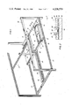
- FIG. 1 is an isometric view of one embodiment of the electroding machine according to the present invention.
- FIG. 2 is a cross-sectional view showing the separation between photovoltaic cells and films formed by operation of the electroding machine.
- FIG. 3 is a cross-sectional view taken across Section 3--3 shown in FIG. 1.
- FIG. 4 is a cross-sectional view of Section 4--4 shown in FIG. 3.
- FIG. 5 is an elevation of the tool head assembly.
- FIG. 1 there may be seen a perspective view of an apparatus depicting one embodiment of the present invention for forming a photovoltaic panel 90 into a plurality of electrically isolated photovoltaic cells and preparing each of the photovoltaic cells for receiving an overlying conducting layer which interconnects the individual photovoltaic cells into a series photovoltaic array.
- Photovoltaic panel 90 is a large area panel having a rigid substrate, which may conveniently be glass, a conducting layer on that substrate, which may conveniently be a non-stoichiometric tin oxide, and one or more layers of semi-conductor materials, such as cadmium sulfide and a nonstoichiometric cuprous sulfide, where each of the layers is formed over the entire substrate surface.
- a rigid substrate which may conveniently be glass
- a conducting layer on that substrate which may conveniently be a non-stoichiometric tin oxide
- semi-conductor materials such as cadmium sulfide and a nonstoichiometric cuprous sulfide
- Photovoltaic panel 90 is placed on substrate indexing plate 10 with one edge bearing against edge strip 13 of base plate 11. There may be a separate material disposed between the edge of panel 90 and strip 13 in order to prevent damage to the edge of photovoltaic panel 90.
- Clamping strip 15, which is resiliently mounted adjacent base plate 11 is urged against an opposing edge of photovoltaic panel 90 by clamping means 16 to secure photovoltaic panel 90 upon indexing plate 10.
- Indexing plate 10 is mounted on traversing carriage 20 and moves along indexing support tracks 19. Indexing plate 10 is movble to a plurality of predetermined positions along traversing carriage 20, and indexing means 31 is used to precisely position indexing plate 10 at each predetermined location.
- drive means 42 is actuated to move traversing carriage 20 along support rails 23, which are conveniently mounted on support frame 40.
- Traversing carriage 20 is driven by the movement of drive wire 29 in the desired direction and moves substantially from one end of frame 40 to the other end of frame 40.
- Drive wire 29 may be conveniently wound about a capstan (not shown) having spiral grooves in order to minimize any slippage.
- the capstan (not shown) is driven by a reversible electric motor (not shown).
- the electric motor (not shown) is controlled by a plurality of switches (not shown) which may conveniently be an operator controlled switch for activating the drive motor (not shown) and a plurality of limit switches (not shown) located at the travel extremes desired for traversing carriage 20 for deactivating the drive motor (not shown). Alignment of traversing carriage 20 is maintained by "V"-rail 26 as traversing carriage 20 moves within frame 40.
- tool head 50 which is vertically movable within support channel 52 and actuated vertically by operating cylinder 54 which is connected to support channel 52.
- operating cylinder 54 which is connected to support channel 52.
- tool head 50 is lowered into operating position, as hereinafter explained.
- tool head 50 is raised by operating cylinder 54 and traversing carriage 20 is returned beneath the raised tool head 50 into position for another cutting pass.
- FIG. 1 there is depicted only one tool head 50. It will be apparent, however, that a plurality of tool heads could be provided to minimize the number of times the traversing carriage 20 must be actuated to complete the separation of photovoltaic panel 90 into a plurality of photovoltaic cells.
- Such additional tool heads could be arranged in a variety of ways, e.g., one beside another or staggered along the path of traversing carriage 20, such arrangement being a matter of choice and determined by the size of tool head 50 and support frame 40. In the extreme, sufficient tool heads are provided for making all of the cuts in one traverse of carriage 20.
- FIG. 2 there may be seen a cross-sectional view through photovoltaic panel 90 illustrating the configuration of the separated photovoltaic cells produced by one pass of photovoltaic panel 90 beneath tool head 50.
- a portion of cadmium sulfide layer 94 and cuprous sulfide layer 95 have been removed to provide a first groove 91 and expose the surface of the tin oxide conducting layer within groove 91.
- a portion of the exposed tin oxide layer 93 is removed, forming the base electrode gap 96 and serving to electrically isolate the individual photovoltaic cells formed by the cadmium sulfide 94 and cuprous sulfide 95 layers overlying each of the isolated tin oxide areas 93.
- Insulating films 97 and 98 may be formed from a variety of materials to which the semi-conductor layers 94 and 95 do not react to reduce cell performance. Materials which have been successfully used include a photo-resist marketed under the trademark KMER by Kodak, polyvinyl chloride films, acrylic paint and cellulose film formers. The insulating materials are generally applied as a high solid content slurry with just enough solvent to enable the slurry to flow through the pen. Insulating materials 97 and 98 are selected based on the particular method chosen to actually separate the overlying conductor layers and form the completed series interconnection. A variety of techniques and the corresponding insulating film requirements are contained in U.S.
- FIG. 2 depicts "adhesive strip" 99 which has been applied to the remaining exposed area of the tin oxide layer 93. It has been found that certain overlying conductor materials do not make a low resistance contact and/or metallurgical bond with the tin oxide when deposited directly on the tin oxide. Thus, an adhesive strip 99 may be provided for the purpose of insuring better electrical contact and/or metallurgical bond between the subsequent conducting layers and the underlying tin oxide layer 93.
- Adhesive strip 99 may be brass, zinc, indium, or some other metal, the selected material being a function of the material forming the overlying conductor. In one embodiment, a rotating wheel contacts the surface of tin oxide layer 93 and a small amount the desired material is abraded onto the surface.
- each of the individual photovoltaic cells consists of a strip of semi-conductor materials extending the entire width of substrate panel 92, each strip having a width in the order of ten millimeters. It has been found that a groove 91 width of about one millimeter is required to accommodate insulation films 97 and 98 and adhesive strip 99. Isolation gap 96 has a width of only about 0.1 millimeter. Thus, approximately ten percent (10%) of the surface area of photovoltaic panel 90 may be required to form the electrical interconnections to produce the series connected solar cell array.
- FIG. 3 there may be seen a cross-sectional view taken along view 3--3 as shown in FIG. 1.
- Photovoltaic panel 90 is resting on base plate 11 with one edge against resilient member 14 and urged against the edge strip 13.
- Resilient member 14 is interposed to minimize damage to substrate materials, some of which are fragile and may be mounted on clamping strip 15 rather than edge strip 13, if desired, to provide a rigid clamp edge for reproducible positioning.
- Photovoltaic panel 90 is urged against strip 13 by a clamping strip 15.
- Clamping strip 15 may be resiliently mounted adjacent base plate 11 with sufficient movement to accommodate slight variations in the size of photovoltaic panel 90.
- a clamp means 16 is provided for urging clamping strip 15 against photovoltaic panel 90 and thereby secure photovoltaic panel 90 on base plate 11.
- Clamp means 16 may be conveniently provided by an eccentric cam rotatably mounted on base plate 11 and which urges clamping strip 15 toward photovoltaic panel 90 as the eccentric cam is rotated about its axis.
- a variety of clamping means are available for securing photovoltaic panel 90 on base plate 11 and only a preferred embodiment is hereinabove discussed.
- the requirements for any such clamping mechanism include maintaining alignment of photovoltaic panel 90 within the clamping mechanism as clamping force is applied and providing sufficient clamping force to resist movement of photovoltaic panel 90 as the assembly is moved beneath the various cutting mechanisms but not enough force to damage photovoltaic panel 90.
- another acceptable clamp might be formed from one or more threaded members engaging strips 13 and 15 for moving strips 13 and 15 with respect to one another and engaging a photovoltaic panel 90 placed therebetween.
- the entire substrate indexing plate 10 is sequentially indexed to a plurality of predetermined locations along traversing carriage 20. At each such location carriage 20 is traversed beneath cutting head 50 (see FIG. 1) within frame 40 to form one or more photovoltaic cell separations.
- An indexing means 30 must be provided to precisely locate photovoltaic panel 90 beneath the cutting head to make each cut.
- an indexing strip 12 is located beneath base plate 11 and may conveniently take the form of a notched bar or strip. Each notch may be "V"-shaped to receive a correspondingly shaped index pin 33 mounted on index lever 31. Index lever 31 pivots about fulcrum 32 and extends beyond the edge of base plate 11 for convenient access.
- Index lever 31 is pulled upwardly to release index pin 33 from indexing means 12 and base plate 11 is moved to position the next index notch above index pin 33 and the lever released, whereby index pin 33 is pivoted about fulcrum 32 to engage the desired index notch in indexing means 12.
- the "V"-shaped engagements insure a high degree of accuracy and repeatability.
- indexing base plate 11 there are many mechanisms available for indexing base plate 11 to a plurality of predetermined positions and only a preferred embodiment is shown in FIG. 3.
- the primary requirement for any such indexing mechanism is to precisely locate photovoltaic panel 90 in order to insure uniform width of the photovoltaic strips produced on photovoltaic panel 90.
- An acceptable alternate mechanism might utilize a lead screw engaging a traveling nut connected to base plate 11 whereby the base plate 11 would be positioned in response to rotation of the lead screw. The lead screw could then be rotated either by hand or by a step motor to produce precise incremental travel. It is within the scope of the present invention to cover any indexing system which obtains the required accuracy, whether manually or mechanically driven or whether manually or automatically actuated.
- Carriage base 22 is supported by wheels 24 which are rotatably mounted on carriage base 22.
- Support wheels 24 ride on support rails 23 which extend the total distance along which the carriage 20 is to traverse.
- the purpose of support wheels 24 and support rails 23 are to carry the weight of photovoltaic panel 90, indexing plate 10 and traversing carriage 20.
- Carriage base 22 must maintain a precise alignment while traversing the tool head in order to insure that the grooves 91 (see FIG. 1) remain parallel. This alignment is obtained by means of a "V"-shaped roller 27 engaging an inverted “V”-shaped track 26 mounted on frame 40. Guide track 26 is precisely positioned in fabricating support frame 40. The mating "V"-shapes minimize any lateral movement of carriage base 20 during traverse of carriage base 22 along support rails 23. Thus, each groove 91 will be formed in a parallel relationship with each adjacent groove.
- Carriage base 22 is depicted supported by support wheels 24 on rail 23.
- Substrate indexing plate 10 is likewise supported on indexing support tracks 19 for movement above carriage base 22.
- Base plate 11 is carried above support tracks 19 on slidable mounting 18 which may conveniently take the form of recirculating ball bushings which are slotted to mate with a bar-shaped portion of indexing support track 19.
- two recirculating ball bushings are mounted on one side of base plate 11 and are rigidly fixed to base plate 11.
- a third recirculating ball bushing is mounted on the other side of base plate 11 and is mounted for self-alignment with its mating indexing support track 19. The self-alignment feature compensates for any deviation from precise parallelism between the two indexing support tracks 19.
- Tool block 58 is provided for housing the various tool components and is affixed to attachment bracket 56 by attachment means which may conveniently take the form of threaded members such as screws or bolts. Attachment bracket 56 is further attached to connecting rod 55 by any acceptable attachment means such as a threaded engagement. Connecting rod 55 is further attached to an operating cylinder 54 (see FIG. 1) which serves to move tool block 58 vertically within channel member 52.
- Tool block 58 houses a variety of tool elements, each of which is hereinbelow discussed. Each element may conveniently have a number of features which provide the same functional relationship for each element and these common features will be discussed for a typical tool member.
- a cam track 59 is provided above the surface of photovoltaic panel 90 and may be conveniently attached to carriage base 22. Cam track 59 engages cam follower 60 on each tool member whereby each tool member is raised against urging means 61 just prior to the tool member engaging the edge of photovoltaic panel 90 and is lowered onto the surface a short distance, typically 1/8 inch or less, after the edge portion passes beneath the tool element. Urging means 61 then maintains vertical stop 62 in engagement with tool block 58 during traverse of the tool element across the surface of photovoltaic panel 90. Urging means 61 may conveniently take the form of a leaf spring which urges vertical stop 62 toward tool block 58 as a cam follower 60 is activated by cam member 59 to cam the tool element over the edge of photovoltaic panel 90.
- a further common feature is lateral adjusting means 64, which may conveniently take the form of a threaded member engaging each tool element housing for lateral adjustment of the tool member within tool block 58.
- lateral adjusting means 64 may conveniently take the form of a threaded member engaging each tool element housing for lateral adjustment of the tool member within tool block 58.
- each of the tool elements must maintain a particular and precise lateral alignment with respect to the lead cutting element which forms groove 91 in order to provide the required configuration for the completed cell separation. This is accomplished by adjusting each element by adjustment means 64 to obtain the correct position within tool block 58.
- Cutting head assembly 68 consists basically of a cutting means 70 which may conveniently take the form of a tungsten carbide-tipped lathe tool bit sharpened to produce a groove about one millimeter wide.
- Tool bit 70 is urged against the surface of photovoltaic panel 90 by a spring means (not shown) which may be contained internally of cutting head 68. It has been found that a spring force of 4-8 pounds provides sufficient pressure at the tool bit 70 tip to fracture the polycrystalline films whereby defined opposing edges are produced as the tool moves along photovoltaic panel 90.
- the polycrystalline layers of cadmium sulfide and cuprous sulfide are relatively easy to remove using the lathe tool bit.
- the tin oxide layer conversely, is not penetrated by the tool bit so that the surface of the tin oxide layer is exposed during removal of the overlying semiconductor films.
- An upper limit on tool bit 70 pressure is produced by the requirement that the tin oxide layer is not removed by the action of tool bit 70.
- a rotating buffer-type wheel might also be used to remove these layers.
- Acceptable materials for forming such a buffer-type wheel would comprise a soft matrix material impregnated with a hard abrasive material: e.g. material commercially available for forming printed circuit boards having glass fibers in a polymer-type matrix; or a rubber matrix containing grains of abrasive material such as tungsten carbide.
- Such rotating wheels have an advantage in not requiring sharpening, but have the disadvantage of producing edge configurations in the polycrystalline layers which are less well defined than the edge configurations produced by the sharpened tool bit. Accordingly, the sharpened tool bit is the preferred cutting element.
- the conductive layer isolating head 72 which is used to remove a portion of the tin oxide layer to electrically isolate adjacent regions of the tin oxide which forms the electrically conductive base for the overlying semiconductor materials. In one embodiment of the present invention, this is accomplished by vaporizing a portion of the tin oxide layer by means of an electrical arc which apparently acts to vaporize the tin oxide immediately under and adjacent the arc.
- An electrode 75 is provided by means of a tungsten wire and it has been found that a tungsten wire having about a 40 mil diameter with a point ground to about 2 mil radius removes an acceptable width of tin oxide whereby the adjacent tin oxide areas are electrically isolated.
- Conductive layer isolating head 72 is laterally adjusted within tool block 58 to direct electrode tip 75 to an exposed portion of tin oxide near one edge of the furrow produced from cutting tip 70. Electrode tip 75 is urged against the tin oxide surface by a spring means (not shown) which may be conveniently located interiorly of head 72. Only a slight pressure of 1/4-1/2 pound is needed to insure contact between the tip of electrode 75 and the tin oxide surface. Electrode tip 75 is supported by an insulating holder 75 which, in turn, is supported by conductive layer isolating head 72. A power supply cord 76 is attached to electrode tip 75 and interconnects with an external voltage supply 77 which provides the required 20-40 volts of d.c. or a.c. power. It should be noted that a ground connection must be provided between the external power supply 77 and the portion of the tin oxide layer toward which the tool head 50 is being indexed in order to complete the electrical circuit.
- insulation applicator heads 78 and 82 may be either insulation applicator heads 78 and 82, which are substantially identical, or adhesive strip applicator head 86.
- Insulation applicator heads 78 and 82 carry insulation applicator pens 79 and 83 which move along opposite edges of the furrow created by tool bit 70 and may be urged against the surface of photovoltaic panel 90 by their own weight or by a slight urging force.
- Applicator pens 79 and 83 are permitted vertical movement along insulation application heads 78 and 82 and are guided in such vertical movement by vertical guide means 80 and 84.
- Vertical guide means 80 and 84 may conveniently take the form of a groove or slot within applicator heads 78 and 82 which are engaged by guide brackets attached to applicator pens 79 and 83.
- urging means 66 may be provided in vertical guide means 80 and 84 to maintain contact between the pen tips and the film surfaces.
- the lateral positions of applicator pens 79 and 83 within tool block 58 are adjusted by lateral adjustment means 64 to provide the pen tips along the edges of the furrow on the surface of photovoltaic panel 90.
- Applicator pens 79 and 83 may be conveniently formed from needles used to provide intravenous injecttions in humans.
- a standard number 25 sized needle has been found to be satisfactory and the only modification required is to slightly roll back the tip to dull the exit region.
- Yet another suitable applicator pen is provided under the trade name Leroy which is commercially available at drafting equipment supply stores.
- the size of each of the applicator pens 79 and 83 is determined by the flow characteristics and viscosity of the particular resins which are being used to form the insulating films.
- Insulation film-forming materials are supplied to applicator pens 79 and 83 by supply lines 81 and 82, respectively, from supply cylinders located apart from tool head 50. Generally, a slight pressurization is required to obtain a smooth and continuous flow of the insulation film-forming materials and the supply cylinders are generally pressurized to about 5 p.s.i.
- a conventional source of compressed air is connected to a regulator which maintains the required pressure which is generally transmitted to the film forming material supply cylinders through a two-way valve whereby the supply cylinders are pressurized only during the traverse of the tool head 50 above the photovoltaic panel 90 in order to prevent any dripping of the film-forming materials during the return traverse of photovoltaic panel 90 beneath the raised tool head 50.
- Adhesive strip applicator head 86 is shown aft of insulation applicator pens 79 and 83 to obtain a preferred mechanical mounting. However, it may be necessary to mount adhesive strip applicator head 86 forward of applicator pens 79 and 83 to prevent an accumulation of material on the buffer wheel or smearing the insulation. Either arrangement may be used within the scope of the invention.
- a buffer wheel and pulley assembly 87 is rotatably mounted on adhesive strip applicator head 86 for abrading a selected material onto the tin oxide surface which remains after a portion has been vaporized.
- the buffer wheel 87 may be brass, zinc or indium, of all which provide an improved contact between the tin oxide layer and an overlying conductor layer.
- a small drive motor 88 may be mounted on tool block 58, driving buffer wheel and pulley assembly 87 through drive belt 89. It is also possible to mount drive motor 88 on support channel 52 and use a flexible cable to connect with and drive buffer wheel 87.
- apparatus is provided to fully prepare a photovoltaic panel for obtaining a plurality of individual photovoltaic cells interconnected into a series array for producing usable quantities of electrical energy.
- a large scale panel is loaded onto indexing plate 10 and securely clamped into position and indexing means 12 is moved to a first position adjacent tool head 50.
- Drive means 42 is actuated, pulling traversing carriage 20 along guide track 26 and beneath tool head 50.
- a cam track 59 mounted on traversing carriage 20 lifts the tool element over the edge and onto the surface of photovoltaic panel 90 for bearing against the surface to perform its specific function.
- a first groove 91 is formed as depicted in FIG.
- a limit switch is engaged which may reverse movement of traversing carriage 20 and actuate operating cylinder 54 to raise tool head 50 and return traversing carriage 20 for another pass.
- a second limit switch is actuated upon the return of traversing carriage 20 and drive means 42 is deactivated.
- Indexing plate 10 is moved to a second position by means of disengaging index pin 33 from one index notch and engaging a second index notch.
- Drive means 42 is again activated and the above process is repeated until the desired number of photovoltaic cells have been separately formed from photovoltaic panel 90.
Abstract
Description
Claims (8)
Priority Applications (1)
| Application Number | Priority Date | Filing Date | Title |
|---|---|---|---|
| US06/084,571 US4228570A (en) | 1979-10-15 | 1979-10-15 | Electroding preparation apparatus |
Applications Claiming Priority (1)
| Application Number | Priority Date | Filing Date | Title |
|---|---|---|---|
| US06/084,571 US4228570A (en) | 1979-10-15 | 1979-10-15 | Electroding preparation apparatus |
Related Parent Applications (1)
| Application Number | Title | Priority Date | Filing Date |
|---|---|---|---|
| US05847784 Continuation | 1977-11-02 |
Publications (1)
| Publication Number | Publication Date |
|---|---|
| US4228570A true US4228570A (en) | 1980-10-21 |
Family
ID=22185819
Family Applications (1)
| Application Number | Title | Priority Date | Filing Date |
|---|---|---|---|
| US06/084,571 Expired - Lifetime US4228570A (en) | 1979-10-15 | 1979-10-15 | Electroding preparation apparatus |
Country Status (1)
| Country | Link |
|---|---|
| US (1) | US4228570A (en) |
Cited By (6)
| Publication number | Priority date | Publication date | Assignee | Title |
|---|---|---|---|---|
| US4292092A (en) * | 1980-06-02 | 1981-09-29 | Rca Corporation | Laser processing technique for fabricating series-connected and tandem junction series-connected solar cells into a solar battery |
| US5389761A (en) * | 1993-09-17 | 1995-02-14 | General Motors Corporation | Method and apparatus for cleaning metal pieces prior to resistive seam welding or laser lap seam welding |
| WO2004002197A1 (en) * | 2002-06-24 | 2003-12-31 | Nobö Electro As | Method and arrangement for manufacturing a glass heating element |
| US20110017276A1 (en) * | 2008-03-31 | 2011-01-27 | Vincenzo Boffa | Sun tracker device |
| US20120312228A1 (en) * | 2011-06-10 | 2012-12-13 | Mimaki Engineering Co., Ltd. | Medium processing device |
| CN114083250A (en) * | 2021-10-20 | 2022-02-25 | 中国华能集团清洁能源技术研究院有限公司 | Photovoltaic module intelligence installation device |
Citations (6)
| Publication number | Priority date | Publication date | Assignee | Title |
|---|---|---|---|---|
| SU217860A1 (en) * | METHOD OF MECHANICAL TREATMENT OF DETAILS, FLAINED WITH A SOLID PLAIN-MELTING | |||
| US2248057A (en) * | 1939-01-25 | 1941-07-08 | Bell Telephone Labor Inc | Electrical cutting device |
| US2680184A (en) * | 1951-02-07 | 1954-06-01 | Duncan B Cox | Method for severing or slitting metal foil |
| US2744451A (en) * | 1952-02-28 | 1956-05-08 | Luther E Lee | Parting and slotting tool |
| US3438354A (en) * | 1966-07-21 | 1969-04-15 | Ciba Ltd | Device for applying marks to photographic paper |
| US3937915A (en) * | 1972-12-19 | 1976-02-10 | Matsushita Electric Industrial Co., Ltd. | Metal working method using electric arc and jet gas and the apparatus therefor |
-
1979
- 1979-10-15 US US06/084,571 patent/US4228570A/en not_active Expired - Lifetime
Patent Citations (6)
| Publication number | Priority date | Publication date | Assignee | Title |
|---|---|---|---|---|
| SU217860A1 (en) * | METHOD OF MECHANICAL TREATMENT OF DETAILS, FLAINED WITH A SOLID PLAIN-MELTING | |||
| US2248057A (en) * | 1939-01-25 | 1941-07-08 | Bell Telephone Labor Inc | Electrical cutting device |
| US2680184A (en) * | 1951-02-07 | 1954-06-01 | Duncan B Cox | Method for severing or slitting metal foil |
| US2744451A (en) * | 1952-02-28 | 1956-05-08 | Luther E Lee | Parting and slotting tool |
| US3438354A (en) * | 1966-07-21 | 1969-04-15 | Ciba Ltd | Device for applying marks to photographic paper |
| US3937915A (en) * | 1972-12-19 | 1976-02-10 | Matsushita Electric Industrial Co., Ltd. | Metal working method using electric arc and jet gas and the apparatus therefor |
Cited By (7)
| Publication number | Priority date | Publication date | Assignee | Title |
|---|---|---|---|---|
| US4292092A (en) * | 1980-06-02 | 1981-09-29 | Rca Corporation | Laser processing technique for fabricating series-connected and tandem junction series-connected solar cells into a solar battery |
| US5389761A (en) * | 1993-09-17 | 1995-02-14 | General Motors Corporation | Method and apparatus for cleaning metal pieces prior to resistive seam welding or laser lap seam welding |
| WO2004002197A1 (en) * | 2002-06-24 | 2003-12-31 | Nobö Electro As | Method and arrangement for manufacturing a glass heating element |
| US20110017276A1 (en) * | 2008-03-31 | 2011-01-27 | Vincenzo Boffa | Sun tracker device |
| US20120312228A1 (en) * | 2011-06-10 | 2012-12-13 | Mimaki Engineering Co., Ltd. | Medium processing device |
| US8887403B2 (en) * | 2011-06-10 | 2014-11-18 | Mimaki Engineering Co., Ltd. | Medium processing device |
| CN114083250A (en) * | 2021-10-20 | 2022-02-25 | 中国华能集团清洁能源技术研究院有限公司 | Photovoltaic module intelligence installation device |
Similar Documents
| Publication | Publication Date | Title |
|---|---|---|
| US5084107A (en) | Solar cell and solar cell array with adhered electrode | |
| US5868869A (en) | Thin film photovoltaic device and process of manufacture | |
| CA1251577A (en) | Apparatus for making scribed circuit boards and circuit board modifications | |
| CA1142614A (en) | Wire harness and a method of manufacturing thereof | |
| US7055570B2 (en) | Automated manufacturing system of lithium secondary battery | |
| US4228570A (en) | Electroding preparation apparatus | |
| US20080210368A1 (en) | Method and Device for Transferring a Chip to a Contact Substrate | |
| JP2000315809A (en) | Fabrication of integrated thin film solar cell and patterning system | |
| EP1149422A1 (en) | Method and apparatus for applying a metallization pattern to a substrate for a photovoltaic cell | |
| CA1325161C (en) | Method and apparatus for forming a polycrystalline monolayer | |
| GB1602391A (en) | Apparatus for applying a layer of pasty material to a carrier through a screen | |
| JP2002033498A (en) | Manufacturing method for integrated thin-film solar cell and patterning apparatus | |
| JP2588885B2 (en) | Lamination and center positioning method and apparatus for laminated glass | |
| US3797103A (en) | Machine and process for semiconductor device assembly | |
| EP1261063A2 (en) | Automated manufacturing system for manufacturing a secondary lithium battery | |
| CN112073006A (en) | Glass substrate preprocessing device | |
| JPH11165250A (en) | Wire saw | |
| US3103137A (en) | Means for securing conductive leads to semiconductive devices | |
| WO1983001173A1 (en) | Device for inserting electric part | |
| CN111745279A (en) | Bus bar electromagnetic welding device | |
| CN211939421U (en) | Confluence welding device and solar cell welding machine | |
| US3669478A (en) | Machine and process for semiconductor device assembly | |
| CN218135343U (en) | Welding strip cutting system | |
| CN218857687U (en) | Automatic high-temperature film pasting device | |
| CN213595545U (en) | Special self-smoothing copper strip machine conveying device for chip clamping electrode plate |
Legal Events
| Date | Code | Title | Description |
|---|---|---|---|
| AS | Assignment |
Owner name: LOF REALTY, INC. Free format text: CHANGE OF NAME;ASSIGNOR:PHOTON POWER, INC.,;REEL/FRAME:004318/0361 Effective date: 19831213 Owner name: TOTAL ENERGIE DEVELOPPEMENT Free format text: ASSIGNMENT OF ASSIGNORS INTEREST.;ASSIGNOR:LOF REALTY, INC.;REEL/FRAME:004324/0501 Effective date: 19840410 |
|
| AS | Assignment |
Owner name: TOTAL ENERGIE DEVELOPPMENT + MESSERSCHMITT-BOLKOW- Free format text: ASSIGNMENT OF ASSIGNORS INTEREST.;ASSIGNOR:TOTAL ENERGIE DEVELOPMENT;REEL/FRAME:005503/0019 Effective date: 19901002 |
|
| AS | Assignment |
Owner name: TOTAL ENERGIE DEVELOPPEMENT, NEW YORK Free format text: ASSIGNMENT OF ASSIGNORS INTEREST.;ASSIGNOR:TOTAL ENERGIE DEVELOPMENT + MESSERSCHMITT-BOLKOW BLOHMGMBH & CO. PHOTOTRONICS O.H.G.;REEL/FRAME:006483/0409 Effective date: 19930331 |