US4244752A - Single mask method of fabricating complementary integrated circuits - Google Patents
Single mask method of fabricating complementary integrated circuits Download PDFInfo
- Publication number
- US4244752A US4244752A US06/017,842 US1784279A US4244752A US 4244752 A US4244752 A US 4244752A US 1784279 A US1784279 A US 1784279A US 4244752 A US4244752 A US 4244752A
- Authority
- US
- United States
- Prior art keywords
- layer
- patterned
- substrate
- channel
- devices
- Prior art date
- Legal status (The legal status is an assumption and is not a legal conclusion. Google has not performed a legal analysis and makes no representation as to the accuracy of the status listed.)
- Expired - Lifetime
Links
Images


Classifications
-
- H—ELECTRICITY
- H01—ELECTRIC ELEMENTS
- H01L—SEMICONDUCTOR DEVICES NOT COVERED BY CLASS H10
- H01L21/00—Processes or apparatus adapted for the manufacture or treatment of semiconductor or solid state devices or of parts thereof
- H01L21/70—Manufacture or treatment of devices consisting of a plurality of solid state components formed in or on a common substrate or of parts thereof; Manufacture of integrated circuit devices or of parts thereof
- H01L21/77—Manufacture or treatment of devices consisting of a plurality of solid state components or integrated circuits formed in, or on, a common substrate
- H01L21/78—Manufacture or treatment of devices consisting of a plurality of solid state components or integrated circuits formed in, or on, a common substrate with subsequent division of the substrate into plural individual devices
- H01L21/82—Manufacture or treatment of devices consisting of a plurality of solid state components or integrated circuits formed in, or on, a common substrate with subsequent division of the substrate into plural individual devices to produce devices, e.g. integrated circuits, each consisting of a plurality of components
- H01L21/822—Manufacture or treatment of devices consisting of a plurality of solid state components or integrated circuits formed in, or on, a common substrate with subsequent division of the substrate into plural individual devices to produce devices, e.g. integrated circuits, each consisting of a plurality of components the substrate being a semiconductor, using silicon technology
- H01L21/8232—Field-effect technology
- H01L21/8234—MIS technology, i.e. integration processes of field effect transistors of the conductor-insulator-semiconductor type
- H01L21/8238—Complementary field-effect transistors, e.g. CMOS
- H01L21/823892—Complementary field-effect transistors, e.g. CMOS with a particular manufacturing method of the wells or tubs, e.g. twin tubs, high energy well implants, buried implanted layers for lateral isolation [BILLI]
-
- H—ELECTRICITY
- H01—ELECTRIC ELEMENTS
- H01L—SEMICONDUCTOR DEVICES NOT COVERED BY CLASS H10
- H01L21/00—Processes or apparatus adapted for the manufacture or treatment of semiconductor or solid state devices or of parts thereof
- H01L21/02—Manufacture or treatment of semiconductor devices or of parts thereof
- H01L21/027—Making masks on semiconductor bodies for further photolithographic processing not provided for in group H01L21/18 or H01L21/34
- H01L21/033—Making masks on semiconductor bodies for further photolithographic processing not provided for in group H01L21/18 or H01L21/34 comprising inorganic layers
-
- H—ELECTRICITY
- H01—ELECTRIC ELEMENTS
- H01L—SEMICONDUCTOR DEVICES NOT COVERED BY CLASS H10
- H01L21/00—Processes or apparatus adapted for the manufacture or treatment of semiconductor or solid state devices or of parts thereof
- H01L21/02—Manufacture or treatment of semiconductor devices or of parts thereof
- H01L21/04—Manufacture or treatment of semiconductor devices or of parts thereof the devices having at least one potential-jump barrier or surface barrier, e.g. PN junction, depletion layer or carrier concentration layer
- H01L21/18—Manufacture or treatment of semiconductor devices or of parts thereof the devices having at least one potential-jump barrier or surface barrier, e.g. PN junction, depletion layer or carrier concentration layer the devices having semiconductor bodies comprising elements of Group IV of the Periodic System or AIIIBV compounds with or without impurities, e.g. doping materials
- H01L21/26—Bombardment with radiation
- H01L21/263—Bombardment with radiation with high-energy radiation
- H01L21/265—Bombardment with radiation with high-energy radiation producing ion implantation
- H01L21/266—Bombardment with radiation with high-energy radiation producing ion implantation using masks
-
- H—ELECTRICITY
- H01—ELECTRIC ELEMENTS
- H01L—SEMICONDUCTOR DEVICES NOT COVERED BY CLASS H10
- H01L21/00—Processes or apparatus adapted for the manufacture or treatment of semiconductor or solid state devices or of parts thereof
- H01L21/70—Manufacture or treatment of devices consisting of a plurality of solid state components formed in or on a common substrate or of parts thereof; Manufacture of integrated circuit devices or of parts thereof
- H01L21/71—Manufacture of specific parts of devices defined in group H01L21/70
- H01L21/76—Making of isolation regions between components
- H01L21/762—Dielectric regions, e.g. EPIC dielectric isolation, LOCOS; Trench refilling techniques, SOI technology, use of channel stoppers
- H01L21/76202—Dielectric regions, e.g. EPIC dielectric isolation, LOCOS; Trench refilling techniques, SOI technology, use of channel stoppers using a local oxidation of silicon, e.g. LOCOS, SWAMI, SILO
- H01L21/76213—Dielectric regions, e.g. EPIC dielectric isolation, LOCOS; Trench refilling techniques, SOI technology, use of channel stoppers using a local oxidation of silicon, e.g. LOCOS, SWAMI, SILO introducing electrical inactive or active impurities in the local oxidation region, e.g. to alter LOCOS oxide growth characteristics or for additional isolation purpose
- H01L21/76216—Dielectric regions, e.g. EPIC dielectric isolation, LOCOS; Trench refilling techniques, SOI technology, use of channel stoppers using a local oxidation of silicon, e.g. LOCOS, SWAMI, SILO introducing electrical inactive or active impurities in the local oxidation region, e.g. to alter LOCOS oxide growth characteristics or for additional isolation purpose introducing electrical active impurities in the local oxidation region for the sole purpose of creating channel stoppers
-
- Y—GENERAL TAGGING OF NEW TECHNOLOGICAL DEVELOPMENTS; GENERAL TAGGING OF CROSS-SECTIONAL TECHNOLOGIES SPANNING OVER SEVERAL SECTIONS OF THE IPC; TECHNICAL SUBJECTS COVERED BY FORMER USPC CROSS-REFERENCE ART COLLECTIONS [XRACs] AND DIGESTS
- Y10—TECHNICAL SUBJECTS COVERED BY FORMER USPC
- Y10S—TECHNICAL SUBJECTS COVERED BY FORMER USPC CROSS-REFERENCE ART COLLECTIONS [XRACs] AND DIGESTS
- Y10S438/00—Semiconductor device manufacturing: process
- Y10S438/965—Shaped junction formation
Definitions
- This invention relates to a method of fabricating high density integrated circuits which method employs a single mask to define all devices in the circuit. More particularly, this invention relates to a method of fabricating complementary MOS integrated circuits.
- Complementary MOS circuits are normally circuits which employ both N channel devices and P channel devices in the same integrated circuit chip.
- N channel devices provide faster switching time but have higher power dissipation than P channel devices.
- these devices switch to the on condition for different polarities of the input signal. Therefore, the complementary design technique uses both P and N channel devices in tandem in a typical inverter circuit so that the inverter consumes power only when it switches.
- the output drivers of the first chip When transferring signals from one integrated circuit chip to another, the output drivers of the first chip must provide large impulses to the next chip being driven. It is important that such power is only consumed during switching, so that there is less continuous power dissipation by the output drivers.
- Ion implantation allows for controlled impurity doses and more shallow and smaller regions to be created in the semiconductor substrate.
- the extensive use of ion implantation requires a less number of thermal processing steps for impurity doping as well as reduction in the use of wet chemicals and toxic gases.
- steps in the fabrication of a semiconductor device by diffusion must be performed in sequence so as to arrive at the desired final structure of the respective devices.
- ion implantation often allows for the order of various steps to be interchanged since the depth of the ion implantation is determined by the energy of the respective ions as they strike the target surface.
- Ion implantation is particularly adapted for the fabrication of an integrated circuit having a plurality of different device structures.
- a prior art example of a method of forming an integrated circuit having a plurality of the different devices in it is the Shappir U.S. Pat. No. 3,921,283.
- the method of Shappir must employ a number of different masks which creates an alignment problem.
- Enhancement mode devices are ones which are normally off if no electrical signal is supplied to their gates while depletion mode devices are normally on if no electrical signal is supplied to their gates.
- devices that are on the brink of the threshold where the voltage in either direction turns them on or off.
- weak depletion devices which are only nominally conducting. So it is desirable to have four different types of thresholds for internal devices as well as having complementary devices. Again, prior art methods require an extra number of masking steps to form the respective devices with the consequential alignment problems which reduced the resolution with which the devices could be created and the resulting packing density.
- the present invention is instructed toward a method of fabricating an integrated circuit having a plurality of different devices, which method employs a single mask to define the active areas of all such devices.
- a silicon oxide-silicon nitride layer is formed on the surface of a silicon wafer so as to define the location of subsequent oxide insulating layers which in turn actually define all the active areas of the circuit.
- Respective active areas for the different devices can then be formed by selective ion implantation.
- a feature then of the present invention resides in the method of fabricating an integrated circuit having a plurality of different devices, which method employs a single mask to define the active areas of all such devices.
- a silicon oxide-silicon nitride layer defines the location of subsequent oxide insulating layers which in turn actually define all the active areas of the circuit.
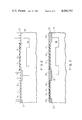
- FIG. 1 is a plan view of the present invention.
- FIGS. 2-14 are cross-sectional views which represent, in sequence, the various steps of the method of the present invention.
- the present invention is directed toward a method of forming an integrated circuit having a plurality of different active devices which method employs a single mask to define all active areas of the integrated circuit. In this manner, masking tolerances can be reduced to a minimum thereby increasing the packing density of the particular integrated circuit.
- the method is directed toward the formation of a plurality of different types of active devices having different threshold values and is particularly directed towards the formation of complementary MOS circuits having both P channel structures and N channel structures.
- the method is directed toward the fabrication of an interconnect structure which is compatible with such different type devices.
- FIG. 1 A particular embodiment of the present invention is illustrated in a plan view, as shown in FIG. 1.
- This view illustrates the structure that results from the method of the present invention and the details thereof will become apparent from the following discussion of that method.
- the method starts with taking a blank P type wafer 10 and oxidizing the surface thereof to form silicon dioxide layer 11 after which, silicon nitride layer 12 is deposited. Such deposition takes place in a low pressure chemical vapor deposition reactor as is well known in the art.
- the structure of FIG. 2 as thus formed then is the starting material "sandwich" formed on the respective oxide and nitride layers.
- this sandwich is that silicon nitride does not allow oxygen to diffuse therethrough and, thus, the sandwich later serves as the mask to define all the active devices that are to be fabricated as will be more fully described below. These active areas are then defined by etching away those portions of the oxide nitride sandwich as illustrated in FIG. 3. As the method progresses, the N portion of the remaining sandwich will later define an N channel device while the P portion of the sandwich will define the P channel structure.
- the wafer surface is then covered with photoresist pattern 13 to define only the P channel device as illustrated in FIG. 4.
- the P channel well 14 is created by the ion implantation of phosphorous which is an N type dopant or impurity. That is to say, the P channel well 14 is formed by an N type implant.
- Photoresist pattern 13 is then removed and the wafer is subjected to a heat treatment process so as to cause the N type dopants to diffuse to form the profile of P channel well 14 as indicated in FIG. 5.
- N and P masks Electrical isolation between the various active structures as indicated by the N and P masks is achieved first by ion implantation of Boron which is a P type dopant as indicated in FIG. 6.
- the P type regions 15 as shown therein serve to protect against N channel field inversion during the operation of the subsequent circuit.
- the implant energy is to be sufficiently low that the dopants do not penetrate through the silicon nitride oxide masks that define the respective N and P active areas.
- the implant is followed by a field oxidation to form oxidation layers 16, as shown in FIG. 7, which are ultimately used for the protection against parasitic inversion during operations of the circuit.
- Oxide dielectric layers 16 are formed on all portions of the inactive area surfaces and, conversely, define all of the active areas on the surface.
- the active areas are protected from oxidation by respective silicon nitride layers 12 of the various N and P masks since, as was indicated above, silicon nitride is inert and a barrier to oxygen.
- the structure as indicated in FIG. 7 indicates that all of the active areas have been formed which are aligned with one another because of the single master mask that has been employed.
- the nitride oxide sandwich masks for both P and N type devices can now be stripped from the wafer surface as the respective active devices have now been defined and isolated by the various field oxidation layers 16 and field implant layers 15.
- Control gate oxide layers 17 are now grown over the exposed surfaces of the wafer which define the active areas as illustrated in FIG. 8.
- the respective ion implantations can now be made in selected areas with different types of dopants so as to control the device thresholds of the respective active devices as has been indicated above.
- the respective N channel devices will be formed in the bulk wafer 10, which is Boron doped.
- Phosphorous ions are employed for the device wells which are to be more negative where the P channel devices will be formed.
- photoresist layers will be employed to protect the devices which are not to be implanted during that step.
- FIGS. 9 and 10 The various control gates now can be formed and also portions of the interconnect structure. These steps are illustrated in FIGS. 9 and 10. As illustrated in FIG. 9, a polysilicon layer 18 which is doped with N+ impurties is deposited over the entire wafer surface. As illustrated in FIG. 10, the respective N channel gates 19 are formed by etching of polysilicon layer 18 (and also oxide layer 17) as are polysilicon interconnect patterns to those gates as shown in FIG. 1. In addition, polysilicon cover 20 is left over the P channel area 14 which, as has been indicated above, is an N type well. As illustrated in FIG. 11, source and drain areas 21 are now formed for the N channel devices by the ion implantation of, in this embodiment, arsenic ions which are of a N+ type.
- the wafer surface is covered with photoresist pattern 22 except in those areas which define the P channel source and drain regions.
- This photoresist layer includes portion 23 which defines P channel gate 25 and its corresponding interconnect.
- P channel gate 25 is formed by etching previous polysilicon layer 20 and underlying gate oxide layer 17 to expose the wafer surface.
- Source and drain regions 24 are now formed by the ion implantation of Boron ions which are a P+ dopant for the P channel devices.
- Photoresist layers 22 and 23 are now removed and the respective devices are covered with a thin oxide layer 26 which is formed during a heat treatment or diffusion step which drives the various junctions to the proper depth. Afterwards, a thick oxide layer can be formed over the entire surface of the wafer or chip to serve as an insulating layer.
- the respective devices are now complete and have a structure as illustrated in FIG. 13.
- the overall complementary circuit is completed by opening appropriate vias in the oxide layer 26 to receive metal connectors 27, 28 and 29 (and also metal connector as shown in FIG. 1).
- the entire circuit structure is then covered with a passivation layer 31 so as to complete the structure of FIG. 14.
- a particular advantage of the present invention is the employment of the N+ polysilicon interconnect structure between the various gates.
- Prior art complementary devices employing polysilicon interconnect structures use both N+ and P+ types of polysilicon over the N channel and P channel devices respectively.
- This construction required shorting straps whenever the two types overlapped in order to prevent the formation of a junction in the interconnect.
- this problem is overcome since both the polysilicon interconnect structure and the corresponding field plates for both the N and P type devices are all of an N+ polysilicon.
- the elimination of the shorting strap allows a circuit layout density increase for the case of complementary structures.
- a method for fabricating an integrated circuit having a plurality of different devices employs a silicon oxide-silicon nitride layer to define the location of subsequent oxide insulating layers which in turn actually define all the active areas of the circuit. Respective areas are then formed by selective ion implantation.
- This method provides for the self-alignment of the respective active devices in integrated circuit which in turn allows for the achievement of higher packing density. Because of this self-alignment, the number of masking steps is reduced without requiring tolerance variation.
Abstract
Description
Claims (9)
Priority Applications (1)
| Application Number | Priority Date | Filing Date | Title |
|---|---|---|---|
| US06/017,842 US4244752A (en) | 1979-03-06 | 1979-03-06 | Single mask method of fabricating complementary integrated circuits |
Applications Claiming Priority (1)
| Application Number | Priority Date | Filing Date | Title |
|---|---|---|---|
| US06/017,842 US4244752A (en) | 1979-03-06 | 1979-03-06 | Single mask method of fabricating complementary integrated circuits |
Publications (1)
| Publication Number | Publication Date |
|---|---|
| US4244752A true US4244752A (en) | 1981-01-13 |
Family
ID=21784840
Family Applications (1)
| Application Number | Title | Priority Date | Filing Date |
|---|---|---|---|
| US06/017,842 Expired - Lifetime US4244752A (en) | 1979-03-06 | 1979-03-06 | Single mask method of fabricating complementary integrated circuits |
Country Status (1)
| Country | Link |
|---|---|
| US (1) | US4244752A (en) |
Cited By (31)
| Publication number | Priority date | Publication date | Assignee | Title |
|---|---|---|---|---|
| US4325169A (en) * | 1979-10-11 | 1982-04-20 | Texas Instruments Incorporated | Method of making CMOS device allowing three-level interconnects |
| WO1982002283A1 (en) * | 1980-12-22 | 1982-07-08 | Ncr Co | Method for fabricating complementary semiconductor devices |
| WO1982003945A1 (en) * | 1981-04-27 | 1982-11-11 | Ncr Co | Process for manufacturing cmos semiconductor devices |
| US4373253A (en) * | 1981-04-13 | 1983-02-15 | National Semiconductor Corporation | Integrated CMOS process with JFET |
| US4374455A (en) * | 1979-10-30 | 1983-02-22 | Rca Corporation | Method for manufacturing a vertical, grooved MOSFET |
| US4385947A (en) * | 1981-07-29 | 1983-05-31 | Harris Corporation | Method for fabricating CMOS in P substrate with single guard ring using local oxidation |
| US4406710A (en) * | 1981-10-15 | 1983-09-27 | Davies Roderick D | Mask-saving technique for forming CMOS source/drain regions |
| US4412375A (en) * | 1982-06-10 | 1983-11-01 | Intel Corporation | Method for fabricating CMOS devices with guardband |
| US4443811A (en) * | 1979-10-03 | 1984-04-17 | Texas Instruments Incorporated | CMOS Integrated circuit device |
| EP0107851A1 (en) * | 1982-10-29 | 1984-05-09 | Tektronix, Inc. | Manufacture of semiconductor devices by the planar method |
| US4454648A (en) * | 1982-03-08 | 1984-06-19 | Mcdonnell Douglas Corporation | Method of making integrated MNOS and CMOS devices in a bulk silicon wafer |
| US4470191A (en) * | 1982-12-09 | 1984-09-11 | International Business Machines Corporation | Process for making complementary transistors by sequential implantations using oxidation barrier masking layer |
| EP0123384A1 (en) * | 1983-02-25 | 1984-10-31 | Western Digital Corporation | Complementary insulated gate field effect integrated circuit structure and process for fabricating the structure |
| US4481705A (en) * | 1983-06-14 | 1984-11-13 | Advanced Micro Devices, Inc. | Process for doping field isolation regions in CMOS integrated circuits |
| US4509991A (en) * | 1983-10-06 | 1985-04-09 | International Business Machines Corporation | Single mask process for fabricating CMOS structure |
| US4558508A (en) * | 1984-10-15 | 1985-12-17 | International Business Machines Corporation | Process of making dual well CMOS semiconductor structure with aligned field-dopings using single masking step |
| US4600445A (en) * | 1984-09-14 | 1986-07-15 | International Business Machines Corporation | Process for making self aligned field isolation regions in a semiconductor substrate |
| US4653177A (en) * | 1985-07-25 | 1987-03-31 | At&T Bell Laboratories | Method of making and selectively doping isolation trenches utilized in CMOS devices |
| US4657602A (en) * | 1980-11-06 | 1987-04-14 | Burroughs Corporation | Integrated complementary transistor circuit at an intermediate stage of manufacturing |
| US4675981A (en) * | 1984-11-26 | 1987-06-30 | Kabushiki Kaisha Toshiba | Method of making implanted device regions in a semiconductor using a master mask member |
| US4707455A (en) * | 1986-11-26 | 1987-11-17 | General Electric Company | Method of fabricating a twin tub CMOS device |
| EP0257328A1 (en) * | 1986-08-11 | 1988-03-02 | Siemens Aktiengesellschaft | Method of producing pn junctions |
| US4925806A (en) * | 1988-03-17 | 1990-05-15 | Northern Telecom Limited | Method for making a doped well in a semiconductor substrate |
| US5286344A (en) * | 1992-06-15 | 1994-02-15 | Micron Technology, Inc. | Process for selectively etching a layer of silicon dioxide on an underlying stop layer of silicon nitride |
| US5348897A (en) * | 1992-12-01 | 1994-09-20 | Paradigm Technology, Inc. | Transistor fabrication methods using overlapping masks |
| US5519244A (en) * | 1979-05-25 | 1996-05-21 | Hitachi, Ltd. | Semiconductor device having aligned semiconductor regions and a plurality of MISFETs |
| US5830789A (en) * | 1996-11-19 | 1998-11-03 | Integrated Device Technology, Inc. | CMOS process forming wells after gate formation |
| US5880036A (en) * | 1992-06-15 | 1999-03-09 | Micron Technology, Inc. | Method for enhancing oxide to nitride selectivity through the use of independent heat control |
| US5956583A (en) * | 1997-06-30 | 1999-09-21 | Fuller; Robert T. | Method for forming complementary wells and self-aligned trench with a single mask |
| US6573151B1 (en) * | 2000-08-22 | 2003-06-03 | Advanced Micro Devices, Inc. | Method of forming zero marks |
| US11152350B2 (en) * | 2018-12-14 | 2021-10-19 | Texas Instruments Incorporated | Dielectric spaced diode |
Citations (12)
| Publication number | Priority date | Publication date | Assignee | Title |
|---|---|---|---|---|
| US3853633A (en) * | 1972-12-04 | 1974-12-10 | Motorola Inc | Method of making a semi planar insulated gate field-effect transistor device with implanted field |
| US3868274A (en) * | 1974-01-02 | 1975-02-25 | Gen Instrument Corp | Method for fabricating MOS devices with a multiplicity of thresholds on a semiconductor substrate |
| US3928081A (en) * | 1973-10-26 | 1975-12-23 | Signetics Corp | Method for fabricating semiconductor devices using composite mask and ion implantation |
| US3983620A (en) * | 1975-05-08 | 1976-10-05 | National Semiconductor Corporation | Self-aligned CMOS process for bulk silicon and insulating substrate device |
| US4001048A (en) * | 1974-06-26 | 1977-01-04 | Signetics Corporation | Method of making metal oxide semiconductor structures using ion implantation |
| US4005450A (en) * | 1970-05-13 | 1977-01-25 | Hitachi, Ltd. | Insulated gate field effect transistor having drain region containing low impurity concentration layer |
| US4009057A (en) * | 1974-08-12 | 1977-02-22 | U.S. Philips Corporation | Method of manufacturing a semiconductor device |
| US4045250A (en) * | 1975-08-04 | 1977-08-30 | Rca Corporation | Method of making a semiconductor device |
| US4046606A (en) * | 1976-05-10 | 1977-09-06 | Rca Corporation | Simultaneous location of areas having different conductivities |
| US4052229A (en) * | 1976-06-25 | 1977-10-04 | Intel Corporation | Process for preparing a substrate for mos devices of different thresholds |
| US4101344A (en) * | 1976-10-25 | 1978-07-18 | U.S. Philips Corporation | Method of manufacturing a semiconductor device |
| US4104784A (en) * | 1976-06-21 | 1978-08-08 | National Semiconductor Corporation | Manufacturing a low voltage n-channel MOSFET device |
-
1979
- 1979-03-06 US US06/017,842 patent/US4244752A/en not_active Expired - Lifetime
Patent Citations (14)
| Publication number | Priority date | Publication date | Assignee | Title |
|---|---|---|---|---|
| US4005450A (en) * | 1970-05-13 | 1977-01-25 | Hitachi, Ltd. | Insulated gate field effect transistor having drain region containing low impurity concentration layer |
| US3853633A (en) * | 1972-12-04 | 1974-12-10 | Motorola Inc | Method of making a semi planar insulated gate field-effect transistor device with implanted field |
| US3928081A (en) * | 1973-10-26 | 1975-12-23 | Signetics Corp | Method for fabricating semiconductor devices using composite mask and ion implantation |
| US3868274B1 (en) * | 1974-01-02 | 1988-07-26 | ||
| US3868274A (en) * | 1974-01-02 | 1975-02-25 | Gen Instrument Corp | Method for fabricating MOS devices with a multiplicity of thresholds on a semiconductor substrate |
| US4001048A (en) * | 1974-06-26 | 1977-01-04 | Signetics Corporation | Method of making metal oxide semiconductor structures using ion implantation |
| US4009057A (en) * | 1974-08-12 | 1977-02-22 | U.S. Philips Corporation | Method of manufacturing a semiconductor device |
| US3983620A (en) * | 1975-05-08 | 1976-10-05 | National Semiconductor Corporation | Self-aligned CMOS process for bulk silicon and insulating substrate device |
| US4045250A (en) * | 1975-08-04 | 1977-08-30 | Rca Corporation | Method of making a semiconductor device |
| US4046606A (en) * | 1976-05-10 | 1977-09-06 | Rca Corporation | Simultaneous location of areas having different conductivities |
| US4104784A (en) * | 1976-06-21 | 1978-08-08 | National Semiconductor Corporation | Manufacturing a low voltage n-channel MOSFET device |
| US4052229A (en) * | 1976-06-25 | 1977-10-04 | Intel Corporation | Process for preparing a substrate for mos devices of different thresholds |
| US4052229B1 (en) * | 1976-06-25 | 1985-01-15 | ||
| US4101344A (en) * | 1976-10-25 | 1978-07-18 | U.S. Philips Corporation | Method of manufacturing a semiconductor device |
Non-Patent Citations (2)
| Title |
|---|
| Enomoto et al., ". . . Oxidation . . . Si.sub.3 N.sub.4 Film . . . "Jap. Journ. Appl. Phys. 17 (1978) 1049. * |
| Enomoto et al., ". . . Oxidation . . . Si3 N4 Film . . . "Jap. Journ. Appl. Phys. 17 (1978) 1049. |
Cited By (37)
| Publication number | Priority date | Publication date | Assignee | Title |
|---|---|---|---|---|
| US5519244A (en) * | 1979-05-25 | 1996-05-21 | Hitachi, Ltd. | Semiconductor device having aligned semiconductor regions and a plurality of MISFETs |
| US4443811A (en) * | 1979-10-03 | 1984-04-17 | Texas Instruments Incorporated | CMOS Integrated circuit device |
| US4325169A (en) * | 1979-10-11 | 1982-04-20 | Texas Instruments Incorporated | Method of making CMOS device allowing three-level interconnects |
| US4374455A (en) * | 1979-10-30 | 1983-02-22 | Rca Corporation | Method for manufacturing a vertical, grooved MOSFET |
| US4657602A (en) * | 1980-11-06 | 1987-04-14 | Burroughs Corporation | Integrated complementary transistor circuit at an intermediate stage of manufacturing |
| WO1982002283A1 (en) * | 1980-12-22 | 1982-07-08 | Ncr Co | Method for fabricating complementary semiconductor devices |
| US4373253A (en) * | 1981-04-13 | 1983-02-15 | National Semiconductor Corporation | Integrated CMOS process with JFET |
| WO1982003945A1 (en) * | 1981-04-27 | 1982-11-11 | Ncr Co | Process for manufacturing cmos semiconductor devices |
| US4382827A (en) * | 1981-04-27 | 1983-05-10 | Ncr Corporation | Silicon nitride S/D ion implant mask in CMOS device fabrication |
| US4385947A (en) * | 1981-07-29 | 1983-05-31 | Harris Corporation | Method for fabricating CMOS in P substrate with single guard ring using local oxidation |
| US4406710A (en) * | 1981-10-15 | 1983-09-27 | Davies Roderick D | Mask-saving technique for forming CMOS source/drain regions |
| US4454648A (en) * | 1982-03-08 | 1984-06-19 | Mcdonnell Douglas Corporation | Method of making integrated MNOS and CMOS devices in a bulk silicon wafer |
| US4412375A (en) * | 1982-06-10 | 1983-11-01 | Intel Corporation | Method for fabricating CMOS devices with guardband |
| EP0107851A1 (en) * | 1982-10-29 | 1984-05-09 | Tektronix, Inc. | Manufacture of semiconductor devices by the planar method |
| US4470191A (en) * | 1982-12-09 | 1984-09-11 | International Business Machines Corporation | Process for making complementary transistors by sequential implantations using oxidation barrier masking layer |
| EP0123384A1 (en) * | 1983-02-25 | 1984-10-31 | Western Digital Corporation | Complementary insulated gate field effect integrated circuit structure and process for fabricating the structure |
| US4481705A (en) * | 1983-06-14 | 1984-11-13 | Advanced Micro Devices, Inc. | Process for doping field isolation regions in CMOS integrated circuits |
| US4509991A (en) * | 1983-10-06 | 1985-04-09 | International Business Machines Corporation | Single mask process for fabricating CMOS structure |
| US4600445A (en) * | 1984-09-14 | 1986-07-15 | International Business Machines Corporation | Process for making self aligned field isolation regions in a semiconductor substrate |
| US4558508A (en) * | 1984-10-15 | 1985-12-17 | International Business Machines Corporation | Process of making dual well CMOS semiconductor structure with aligned field-dopings using single masking step |
| US4675981A (en) * | 1984-11-26 | 1987-06-30 | Kabushiki Kaisha Toshiba | Method of making implanted device regions in a semiconductor using a master mask member |
| US4653177A (en) * | 1985-07-25 | 1987-03-31 | At&T Bell Laboratories | Method of making and selectively doping isolation trenches utilized in CMOS devices |
| EP0257328A1 (en) * | 1986-08-11 | 1988-03-02 | Siemens Aktiengesellschaft | Method of producing pn junctions |
| US4808542A (en) * | 1986-08-11 | 1989-02-28 | Siemens Aktiengesellschaft | Process for the stabilization of PN junctions |
| US4707455A (en) * | 1986-11-26 | 1987-11-17 | General Electric Company | Method of fabricating a twin tub CMOS device |
| US4925806A (en) * | 1988-03-17 | 1990-05-15 | Northern Telecom Limited | Method for making a doped well in a semiconductor substrate |
| US5286344A (en) * | 1992-06-15 | 1994-02-15 | Micron Technology, Inc. | Process for selectively etching a layer of silicon dioxide on an underlying stop layer of silicon nitride |
| US5880036A (en) * | 1992-06-15 | 1999-03-09 | Micron Technology, Inc. | Method for enhancing oxide to nitride selectivity through the use of independent heat control |
| US6015760A (en) * | 1992-06-15 | 2000-01-18 | Micron Technology, Inc. | Method for enhancing oxide to nitride selectivity through the use of independent heat control |
| US6287978B1 (en) | 1992-06-15 | 2001-09-11 | Micron Technology, Inc. | Method of etching a substrate |
| US20020000423A1 (en) * | 1992-06-15 | 2002-01-03 | Micron Technologies, Inc. | Method for enhancing oxide to nitride selectivity through the use of independent heat control |
| US7049244B2 (en) | 1992-06-15 | 2006-05-23 | Micron Technology, Inc. | Method for enhancing silicon dioxide to silicon nitride selectivity |
| US5348897A (en) * | 1992-12-01 | 1994-09-20 | Paradigm Technology, Inc. | Transistor fabrication methods using overlapping masks |
| US5830789A (en) * | 1996-11-19 | 1998-11-03 | Integrated Device Technology, Inc. | CMOS process forming wells after gate formation |
| US5956583A (en) * | 1997-06-30 | 1999-09-21 | Fuller; Robert T. | Method for forming complementary wells and self-aligned trench with a single mask |
| US6573151B1 (en) * | 2000-08-22 | 2003-06-03 | Advanced Micro Devices, Inc. | Method of forming zero marks |
| US11152350B2 (en) * | 2018-12-14 | 2021-10-19 | Texas Instruments Incorporated | Dielectric spaced diode |
Similar Documents
| Publication | Publication Date | Title |
|---|---|---|
| US4244752A (en) | Single mask method of fabricating complementary integrated circuits | |
| EP0074215B1 (en) | Cmos devices with self-aligned channel stops | |
| US5024965A (en) | Manufacturing high speed low leakage radiation hardened CMOS/SOI devices | |
| US4422885A (en) | Polysilicon-doped-first CMOS process | |
| US4319395A (en) | Method of making self-aligned device | |
| EP0387999B1 (en) | Process for forming high-voltage and low-voltage CMOS transistors on a single integrated circuit chip | |
| US5573963A (en) | Method of forming self-aligned twin tub CMOS devices | |
| KR100564180B1 (en) | Semiconductor integrated circuit device and process for manufacturing the same | |
| US5682051A (en) | CMOS integrated circuit with reduced susceptibility to PMOS punchthrough | |
| US4943537A (en) | CMOS integrated circuit with reduced susceptibility to PMOS punchthrough | |
| US4849364A (en) | Semiconductor devices | |
| US4825278A (en) | Radiation hardened semiconductor devices | |
| US3898105A (en) | Method for making FET circuits | |
| KR900008207B1 (en) | Semiconductor memory device | |
| US4135955A (en) | Process for fabricating high voltage cmos with self-aligned guard rings utilizing selective diffusion and local oxidation | |
| EP0104233A1 (en) | Process for forming complementary integrated circuit devices | |
| EP0465045B1 (en) | Method of field effect transistor fabrication for integrated circuits | |
| US6274914B1 (en) | CMOS integrated circuits including source/drain plug | |
| EP0545082B1 (en) | Process for manufacturing MOS-type integrated circuits comprising LOCOS isolation regions | |
| US5851865A (en) | Method of manufacturing semiconductor device having mask layer forming step for ion implantation | |
| US4471523A (en) | Self-aligned field implant for oxide-isolated CMOS FET | |
| JPH0361338B2 (en) | ||
| US4657602A (en) | Integrated complementary transistor circuit at an intermediate stage of manufacturing | |
| KR920005511B1 (en) | Semiconductor device and its manufacturing method | |
| KR20010074630A (en) | Method of making shallow junction semiconductor devices |
Legal Events
| Date | Code | Title | Description |
|---|---|---|---|
| AS | Assignment |
Owner name: BURROUGHS CORPORATION Free format text: MERGER;ASSIGNORS:BURROUGHS CORPORATION A CORP OF MI (MERGED INTO);BURROUGHS DELAWARE INCORPORATEDA DE CORP. (CHANGED TO);REEL/FRAME:004312/0324 Effective date: 19840530 |
|
| AS | Assignment |
Owner name: SAMSUNG SEMICONDUCTOR AND TELECOMMUNICATIONS, LTD. Free format text: ASSIGNMENT OF ASSIGNORS INTEREST.;ASSIGNOR:UNISYS CORPORATION, A CORP. OF DE.;REEL/FRAME:004998/0745 Effective date: 19870805 Owner name: SAMSUNG SEMICONDUCTOR AND TELECOMMUNICATIONS, LTD. Free format text: ASSIGNMENT OF ASSIGNORS INTEREST;ASSIGNOR:UNISYS CORPORATION, A CORP. OF DE.;REEL/FRAME:004998/0745 Effective date: 19870805 |
|
| AS | Assignment |
Owner name: SAMSUNG SEMICONDUCTOR AND TELECOMMUNICATIONS, LTD. Free format text: ASSIGNMENT OF ASSIGNORS INTEREST.;ASSIGNOR:BURROUGHS CORPORATION;REEL/FRAME:004990/0682 Effective date: 19881027 |
|
| AS | Assignment |
Owner name: SAMSUNG ELECTRONICS CO., LTD., KOREA, REPUBLIC OF Free format text: CHANGE OF NAME;ASSIGNOR:SAMSUNG SEMICONDUCTOR AND TELECOMMUNICATIONS, LTD.;REEL/FRAME:007194/0606 Effective date: 19911210 |