US4274138A - Stored program control system with switching between instruction word systems - Google Patents
Stored program control system with switching between instruction word systems Download PDFInfo
- Publication number
- US4274138A US4274138A US06/011,912 US1191279A US4274138A US 4274138 A US4274138 A US 4274138A US 1191279 A US1191279 A US 1191279A US 4274138 A US4274138 A US 4274138A
- Authority
- US
- United States
- Prior art keywords
- instruction
- word
- sequence
- universal
- program
- Prior art date
- Legal status (The legal status is an assumption and is not a legal conclusion. Google has not performed a legal analysis and makes no representation as to the accuracy of the status listed.)
- Expired - Lifetime
Links
Images


Classifications
-
- G—PHYSICS
- G06—COMPUTING; CALCULATING OR COUNTING
- G06F—ELECTRIC DIGITAL DATA PROCESSING
- G06F9/00—Arrangements for program control, e.g. control units
- G06F9/06—Arrangements for program control, e.g. control units using stored programs, i.e. using an internal store of processing equipment to receive or retain programs
- G06F9/46—Multiprogramming arrangements
- G06F9/48—Program initiating; Program switching, e.g. by interrupt
- G06F9/4806—Task transfer initiation or dispatching
- G06F9/4812—Task transfer initiation or dispatching by interrupt, e.g. masked
-
- G—PHYSICS
- G05—CONTROLLING; REGULATING
- G05B—CONTROL OR REGULATING SYSTEMS IN GENERAL; FUNCTIONAL ELEMENTS OF SUCH SYSTEMS; MONITORING OR TESTING ARRANGEMENTS FOR SUCH SYSTEMS OR ELEMENTS
- G05B19/00—Programme-control systems
- G05B19/02—Programme-control systems electric
- G05B19/04—Programme control other than numerical control, i.e. in sequence controllers or logic controllers
- G05B19/05—Programmable logic controllers, e.g. simulating logic interconnections of signals according to ladder diagrams or function charts
- G05B19/052—Linking several PLC's
-
- G—PHYSICS
- G05—CONTROLLING; REGULATING
- G05B—CONTROL OR REGULATING SYSTEMS IN GENERAL; FUNCTIONAL ELEMENTS OF SUCH SYSTEMS; MONITORING OR TESTING ARRANGEMENTS FOR SUCH SYSTEMS OR ELEMENTS
- G05B2219/00—Program-control systems
- G05B2219/10—Plc systems
- G05B2219/13—Plc programming
- G05B2219/13001—Interrupt handling
-
- G—PHYSICS
- G05—CONTROLLING; REGULATING
- G05B—CONTROL OR REGULATING SYSTEMS IN GENERAL; FUNCTIONAL ELEMENTS OF SUCH SYSTEMS; MONITORING OR TESTING ARRANGEMENTS FOR SUCH SYSTEMS OR ELEMENTS
- G05B2219/00—Program-control systems
- G05B2219/10—Plc systems
- G05B2219/15—Plc structure of the system
- G05B2219/15103—Microprogram stored in rom or ram
-
- G—PHYSICS
- G05—CONTROLLING; REGULATING
- G05B—CONTROL OR REGULATING SYSTEMS IN GENERAL; FUNCTIONAL ELEMENTS OF SUCH SYSTEMS; MONITORING OR TESTING ARRANGEMENTS FOR SUCH SYSTEMS OR ELEMENTS
- G05B2219/00—Program-control systems
- G05B2219/10—Plc systems
- G05B2219/15—Plc structure of the system
- G05B2219/15127—Bit and word, byte oriented instructions, boolean and arithmetic operations
Definitions
- This invention relates to a stored program type control system utilizing a micro-processor.
- a prior art control system of the type referred to above has been fabricated with integrated circuits such as a TTL (transistor-transistor logic) and considered as a mini-computer which is used exclusively to act as a sequence controller for efficiently executing a sequence.
- TTL transistor-transistor logic
- a microprocessor fabricated using LSI techniques was developed which is extremely advantageous from the standpoint of cost and reliability.
- a sequence controller it is necessary to use universal instruction words which are utilized in a micro-processor in view of the requirements for improving the data transmission function and self-detection of faults.
- a stored program type control system comprising a main memory device for storing data and an instruction word, an input/output device for exchanging data with an external apparatus, and a central processing unit including a group of general registers and means storing a program status word and controlling the main memory device and the input/output device, characterized by comprising an instruction word system including a universal instruction word system, and a sequence instruction word system containing a portion of the universal instruction word system which affect the content of a program status word, a portion of the bits of the program status word indicating selection of either the universal instruction word system or the sequence instruction word system, and means responsive to an instruction word or an internal processing operation performed at the time of an interruption condition for selecting one of the instruction word systems depending on the contents of the bit portion of the program status word.
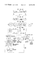
- FIG. 1 is a block diagram showing a stored program type control system of this invention having two instruction systems
- FIG. 2 is a diagram showing the construction of a program status word utilized in this invention
- FIG. 3 is a flow chart showing the operation of this invention.
- FIG. 4 shows the construction of a universal instruction word utilized in a conventional electronic computer
- FIG. 5 shows the construction of a bit processing instruction utilized in this invention
- FIG. 6a shows a logic program
- FIG. 6b shows a ladder program
- FIG. 7 shows the detail of the central processing unit shown in FIG. 1.
- a sequence controller shown in FIG. 1 and provided with two instruction systems comprises a central processing unit (CPU) 30 which may be a micro-processor constructed as a LSI circuit, a first read only memory device ROM 1 32 utilized to store a micro-program constructed by universal instruction words, and a second read only memory device ROM 2 33 utilized to store a micro-program constructed by sequence instruction words.
- CPU central processing unit
- ROM 1 32 utilized to store a micro-program constructed by universal instruction words
- ROM 2 33 utilized to store a micro-program constructed by sequence instruction words.
- the control system further comprises a bus control unit BCU which controls the transfer of data between the central processing unit (CPU) 30 and a memory device (M) 34 and an input/output device (I/O) 35 which generally represents a process input/output device for the control device for transmitting and receiving data, etc.
- the memory device 34 herein used functions to store a program written with universal instruction words, a program written with sequence instruction words and data.
- the memory device M and the input/output device I/O are connected to the bus control unit BCU via a common or separate bus lines. The detail of the central processing unit will be described later with reference to FIG. 7.
- a central processing unit CPU of any type utilizes program status words PSW comprising an address LOC containing a program to be executed next, a condition code CC for storing the result of processing, and status parts showing interruption OK/not OK, etc.
- program status words PSW comprising an address LOC containing a program to be executed next, a condition code CC for storing the result of processing, and status parts showing interruption OK/not OK, etc.
- the result of execution thereof is stored in the condition code CC.
- the 11th bit of the program status word PSW is used as a bit I which represents an instruction word and this bit is used to switch to one of the instruction word systems.
- the difference between a universal instruction word and a sequence instruction word is as follows.
- the universal instruction word is a machine word generally used in a computer and FIG. 4 of the accompanying drawing shows the construction of a mechanic word utilized in TOSBAC-4OL type computer manufactured by the assignee of the present application.
- a word has 16 or 32 bits, for example, of which 8 bits comprise an operation code (OP), each 4 following bits comprises a register designation code (R 1 , R 2 ) and 16 bits comprise imitation data or an address code (A) for transferring data between registers or between registers and addresses or performing computation of the data.
- OP operation code
- R 1 , R 2 register designation code
- A address code
- LOAD instruction a LOAD instruction
- STORE instruction an ADD instruction
- MULTIPLY instruction a LOAD PSW (program status word) instruction.
- LOAD PSW program status word
- the sequence instruction word mainly designates an instruction for processing bits necessary for a sequence controller and contains a portion of the universal instruction.
- bit processing instructions include AND, OR, AND/OR, OR/AND, AND/OR*, OR/AND* and OUT instructions.
- bit processing instructions also includes a TIMER instruction, a SINGLE SHOT instruction, etc., necessary for a sequence controller.
- parentheses show contents of registers or memory devices, AND, OR, etc., represent operation codes and BR 1 and BR 2 represent bit registers showing the results of the logical operations.
- a bit processing instruction comprises 16 bits including an operation code (OP), a device number (DVNO) designating an operand which executes a bit computation, and a negation (N) showing that whether an operand is to be logically negated or not.
- DV described above takes a value that negates the bit state represented by DVNO when N holds whereas a value that does not negate the bit state when N does not hold. In other words, when a bit state is applied, the following equation holds:
- the bit processing instruction may be used as a portion of the universal instruction word without using the operation code of the universal instruction word.
- the operation code is long (8 bits)
- the word is constructed with 16 bits
- the number of the devices that can be designated decreases. Accordingly, when one instruction word is constructed with 32 bits, not only the memory space but also the execution time become inefficient. For this reason, it is necessary to provide a instruction system that can be exclusively used to process bits.
- FIG. 6a shows a logic diagram or a so-called contactless diagram showing one example utilizing a sequence instruction of this invention
- FIG. 6b shows a ladder diagram corresponding to FIG. 6a.
- an AND gate circuit is abbreviated as A.
- the symbol * applied to AND/OR and OR/AND means the beginning portions of the instructions AND/OR and OR/AND and as above described the processings of the beginning portions and remaining portions are different. Accordingly, there is provided a flip-flop circuit that represents the beginning portion of the sequence and the flip-flop circuit is set at the end of the processing of an OUT instruction that represents the end of a sequence and reset at the end of the processing of another instruction to represent again the beginning portion of the sequence.
- BR 1 , BR 2 , and the FLIP-FLOP that represents the start of a sequence are stored as a portion of a condition code of the PSW, so that the controller can resume the original state regardless of an instant at which an interruption is made.
- these parameters may be stored in a general register, and may be saved to a memory device when an interruption is made.
- a sequence instruction word comprises a bit processing instruction
- it also includes such portions of a universal instruction word as a LOAD instruction, a PSW instruction and an EXCHANGE PSW instruction.
- the construction of such instruction word is the same as above described and determined such that the operation code would not overlap a bit processing instruction.
- FIG. 3 is a flow chart showing one example of a typical operation performed at the time of interruption. According to the prior art method since steps 14 and 19 are not provided, they will not be described in the first explanation of the illustrated processing.
- the central processing unit CPU judges the cause of the interruption at step 11 for determining where the present PSW is to be stored or saved and from which address the new PSW should be loaded.
- the present PSW is stored as an old PSW in a memory device while in step 13 a new PSW is loaded, for executing the interruption processing program at steps 15 and 16 by a program from an address expressed by the LOC of the PSW. Steps up to step 13 are executed by the micro-program contained in the central processing unit.
- step 16 the interruption processing is performed and then a return instruction is executed to resume the status before interruption.
- Steps 17 through 20 correspond to the return instruction of the micro-program.
- a PSW stored at step 12 is loaded as a new PSW and a location counter (LOC), not shown, and other condition codes are returned to their original locations at the time of the interruption at step 20.
- LOC location counter
- next control is determined and the PSW is changed. Accordingly, subsequent to steps 13 and 18, steps 14 and 19 are respectively added for determining a new instruction word by bit I of the PSW.
- FIG. 7 shows the detail of the central processing unit CPU shown in FIG. 1.
- the flow chart shown in FIG. 3 will be described in terms of hardware shown in FIG. 7.
- the CPU 30 shown in FIG. 7 comprises an instruction register (IR) 40, a ROM address register (RAR) 41, ROM 1 32, ROM 2 33, a decoder 42, a program status word (PSW) store 44, an arithmetic logic unit (ALU) 45 and register 46.
- IR instruction register
- RAR ROM address register
- PSW program status word
- ALU arithmetic logic unit
- the content of an address represented by a location counter LOC, not shown, of the PSW in store 44 is read out from memory device 34 through bus control unit (BCU) 31 and then stored in the instruction register (IR) 40.
- the ROM address register (RAR) 41 is operated in accordance with the instruction word stored in the instruction register 40 and PSW to designate a specific address of either one of ROM 1 32 and ROM 2 33.
- the content read out from either one of the ROMs is decoded by decoder 42 to produce control signals 43a and 43b to control various circuits in the CPU 30, and the bus control unit (BCU) 31 and to determine the address of ROMs.
- ALU arithmetic logic unit
- Execution of an instruction word is performed by a group of data read out from either one of the ROMs.
- the data content of a ROM corresponds to the program of the content of the memory device 34 and is called a microprogram.
- the circuit shown in FIG. 7 operates as follows. When an interruption is made while a program of an instruction system is being executed the microprogram judges whether the interruption is made at the beginning of the instruction or not. Thus, the instruction is applied to the registers 46 via BCU 31 to check the instruction.
- the interruptions may be classified into an external interruption and an internal interruption and where the interruption should be processed by programs as desired (for example, an immediate interruption or an illegal instruction interruption) other than those which can be processed at a microprogram level (for example, a channel I/O processing), the addresses which store old and new PSW are determined by the device number of the input/output device 35.
- the I/O device number is acknowledged by the microprogram and a current PSW which has been stored in PSW store 44 is saved to a specific address of the memory device 34 via BCU 31 to read out a new PSW from the specific address of the memory device and store it in PSW 44. Then by the I bit of the PSW, the type of instruction word to be executed next is determined so as to select either one of ROM 1 or ROM 2 .
- the description described above concerns steps 11, 12, 13 and 14 shown in FIG. 3 and these steps are executed at a microprogram level, whereas at step 16 the instruction is executed at an ordinary program level.
- Steps 18 and 19 constitutes a return instruction in which the address of an old PSW previously stored is designated and read out from the memory device 34 and then stored in PSW store 44 via BCU 31 as a current PSW. Now the I bit of PSW determines the type of the instruction word to be executed next thus resuming the status before interruption.
- Symbols 15 and 17 merely represents NODES.
- the invention provides an efficient sequence controller utilizing sequence instruction words as the universal instruction words and can be executed by a micro-processor or a universal controller utilizing a single or a plurality of instruction words in addition to universal instruction words which are selectively used and the informations thereof are contained in the program status words.
Abstract
In a stored program type control system comprising a main memory device for storing data and an instruction word, an input/output device, and a central processing unit including a group of general registers and a program status word store, there are provided an instruction word system including a universal instruction word system, and a sequence instruction system containing a portion of the universal word system which control the content of a program status word, and selecting means responsive to an instruction word or an internal processing sequence at the time of interruption for selecting one or the other of the instruction word systems in accordance with data contained at a portion of the bits of the program status words indicates selection of either the universal status word system or the sequence instruction word system.
Description
This invention relates to a stored program type control system utilizing a micro-processor.
A prior art control system of the type referred to above has been fabricated with integrated circuits such as a TTL (transistor-transistor logic) and considered as a mini-computer which is used exclusively to act as a sequence controller for efficiently executing a sequence. As a result of recent advances in semiconductor techniques, however, a microprocessor fabricated using LSI techniques was developed which is extremely advantageous from the standpoint of cost and reliability. In a sequence controller, it is necessary to use universal instruction words which are utilized in a micro-processor in view of the requirements for improving the data transmission function and self-detection of faults.
For this reason, it has been the practice to use both universal instruction words and sequence instruction words making it desirable (1) to use a program written with universal instruction words, without any modification, and (2) to execute an interruption processing program with either the universal instruction words or the sequence instruction words and to return to the original instruction words when the execution of the interruption processing program is completed.
It is an object of this invention to provide an improved stored program type control system capable of efficiently processing an interruption without modifying a program.
According to this invention there is provided a stored program type control system comprising a main memory device for storing data and an instruction word, an input/output device for exchanging data with an external apparatus, and a central processing unit including a group of general registers and means storing a program status word and controlling the main memory device and the input/output device, characterized by comprising an instruction word system including a universal instruction word system, and a sequence instruction word system containing a portion of the universal instruction word system which affect the content of a program status word, a portion of the bits of the program status word indicating selection of either the universal instruction word system or the sequence instruction word system, and means responsive to an instruction word or an internal processing operation performed at the time of an interruption condition for selecting one of the instruction word systems depending on the contents of the bit portion of the program status word.
In the accompanying drawings:
FIG. 1 is a block diagram showing a stored program type control system of this invention having two instruction systems;
FIG. 2 is a diagram showing the construction of a program status word utilized in this invention;
FIG. 3 is a flow chart showing the operation of this invention;
FIG. 4 shows the construction of a universal instruction word utilized in a conventional electronic computer;
FIG. 5 shows the construction of a bit processing instruction utilized in this invention;
FIG. 6a shows a logic program;
FIG. 6b shows a ladder program; and
FIG. 7 shows the detail of the central processing unit shown in FIG. 1.
A sequence controller shown in FIG. 1 and provided with two instruction systems comprises a central processing unit (CPU) 30 which may be a micro-processor constructed as a LSI circuit, a first read only memory device ROM 1 32 utilized to store a micro-program constructed by universal instruction words, and a second read only memory device ROM 2 33 utilized to store a micro-program constructed by sequence instruction words. These read only memory devices are not used simultaneously and each memory device contains a program for switching to the other, and the central processing unit CPU is controlled by the micro-programs of the read only memory devices.
The control system further comprises a bus control unit BCU which controls the transfer of data between the central processing unit (CPU) 30 and a memory device (M) 34 and an input/output device (I/O) 35 which generally represents a process input/output device for the control device for transmitting and receiving data, etc. The memory device 34 herein used functions to store a program written with universal instruction words, a program written with sequence instruction words and data. The memory device M and the input/output device I/O are connected to the bus control unit BCU via a common or separate bus lines. The detail of the central processing unit will be described later with reference to FIG. 7.
A central processing unit CPU of any type utilizes program status words PSW comprising an address LOC containing a program to be executed next, a condition code CC for storing the result of processing, and status parts showing interruption OK/not OK, etc. In response to a sequence instruction, the result of execution thereof is stored in the condition code CC. As shown in FIG. 2, according to this invention the 11th bit of the program status word PSW is used as a bit I which represents an instruction word and this bit is used to switch to one of the instruction word systems.
The difference between a universal instruction word and a sequence instruction word is as follows. The universal instruction word is a machine word generally used in a computer and FIG. 4 of the accompanying drawing shows the construction of a mechanic word utilized in TOSBAC-4OL type computer manufactured by the assignee of the present application. Thus, a word has 16 or 32 bits, for example, of which 8 bits comprise an operation code (OP), each 4 following bits comprises a register designation code (R1, R2) and 16 bits comprise imitation data or an address code (A) for transferring data between registers or between registers and addresses or performing computation of the data. Among universal instructions are included a LOAD instruction, a STORE instruction, an ADD instruction, a MULTIPLY instruction, and a LOAD PSW (program status word) instruction. Thus, by using combinations of these instructions, the computer executes its own programs.
On the other hand, the sequence instruction word mainly designates an instruction for processing bits necessary for a sequence controller and contains a portion of the universal instruction.
For example, bit processing instructions include AND, OR, AND/OR, OR/AND, AND/OR*, OR/AND* and OUT instructions. Although not described herein the bit processing instructions also includes a TIMER instruction, a SINGLE SHOT instruction, etc., necessary for a sequence controller.
Principal instructions have the contents as follows:
______________________________________
AND     (BR.sub.1)Λ(DV) → (BR.sub.1)
                             (except at the
                             beginning
                             of the sequence)
        (DV) → (BR.sub.1)
                             (only at the
                             beginning
                             of the sequence)
OR      (BR.sub.1)V(DV) → (BR.sub.1)
                             (except at the
                             beginning
                             of the sequence)
        (DV) → (BR.sub.1)
                             (only at the
                             beginning
                             of the sequence)
AND/OR  (BR.sub.2)V(BR.sub.1)Λ(DV) → (BR.sub.1)
AND/OR* (BR.sub.1) → (BR.sub.2)
        (DV) → (BR.sub.1)
OR/AND  (BR.sub.2)Λ[(BR.sub.1)V(DV)]  → (BR.sub. 1)
OR/AND* (BR.sub.1) → (BR.sub.2)
        (DV) → (BR.sub.1)
OUT     (BR.sub.1) → (DV)
______________________________________
where parentheses () show contents of registers or memory devices, AND, OR, etc., represent operation codes and BR1 and BR2 represent bit registers showing the results of the logical operations.
As shown in FIG. 5, a bit processing instruction comprises 16 bits including an operation code (OP), a device number (DVNO) designating an operand which executes a bit computation, and a negation (N) showing that whether an operand is to be logically negated or not. DV described above takes a value that negates the bit state represented by DVNO when N holds whereas a value that does not negate the bit state when N does not hold. In other words, when a bit state is applied, the following equation holds:
(DV)=[N Λ(DVNO)] V [N Λ(DVNO)]
To produce the content of BR1, (N) is not used so that
(DVNO)=(DV).
The operations of the principal instructions described above are logical operations utilizing combinations of BR1, BR2 and DV.
If desired, the bit processing instruction may be used as a portion of the universal instruction word without using the operation code of the universal instruction word. However, as the operation code is long (8 bits), if the word is constructed with 16 bits, the number of the devices that can be designated decreases. Accordingly, when one instruction word is constructed with 32 bits, not only the memory space but also the execution time become inefficient. For this reason, it is necessary to provide a instruction system that can be exclusively used to process bits.
FIG. 6a shows a logic diagram or a so-called contactless diagram showing one example utilizing a sequence instruction of this invention, and FIG. 6b shows a ladder diagram corresponding to FIG. 6a. When the logic diagram shown in FIG. 6a is programmed the following results are obtained.
______________________________________
        OR            1
        OR            N, 2
        OR            3
        A             4
        A             5
        A/OR*         6
        A/OR          N, 7
        OR/A*         8
        OR/A          9
        OUT           32
______________________________________
In this manner respective instructions are stored in a memory device and executed as above described. In FIG. 6a, an AND gate circuit is abbreviated as A. The symbol * applied to AND/OR and OR/AND means the beginning portions of the instructions AND/OR and OR/AND and as above described the processings of the beginning portions and remaining portions are different. Accordingly, there is provided a flip-flop circuit that represents the beginning portion of the sequence and the flip-flop circuit is set at the end of the processing of an OUT instruction that represents the end of a sequence and reset at the end of the processing of another instruction to represent again the beginning portion of the sequence.
In this embodiment, BR1, BR2, and the FLIP-FLOP that represents the start of a sequence are stored as a portion of a condition code of the PSW, so that the controller can resume the original state regardless of an instant at which an interruption is made.
Instead of storing these parameters as a portion of the condition code they may be stored in a general register, and may be saved to a memory device when an interruption is made.
Although a substantial portion of a sequence instruction word comprises a bit processing instruction, it also includes such portions of a universal instruction word as a LOAD instruction, a PSW instruction and an EXCHANGE PSW instruction. The construction of such instruction word is the same as above described and determined such that the operation code would not overlap a bit processing instruction.
FIG. 3 is a flow chart showing one example of a typical operation performed at the time of interruption. According to the prior art method since steps 14 and 19 are not provided, they will not be described in the first explanation of the illustrated processing. When an interruption signal is received at step 10, the central processing unit CPU judges the cause of the interruption at step 11 for determining where the present PSW is to be stored or saved and from which address the new PSW should be loaded. At step 12, the present PSW is stored as an old PSW in a memory device while in step 13 a new PSW is loaded, for executing the interruption processing program at steps 15 and 16 by a program from an address expressed by the LOC of the PSW. Steps up to step 13 are executed by the micro-program contained in the central processing unit.
At step 16, the interruption processing is performed and then a return instruction is executed to resume the status before interruption.
According to this invention, at the time of interruption, the next control is determined and the PSW is changed. Accordingly, subsequent to steps 13 and 18, steps 14 and 19 are respectively added for determining a new instruction word by bit I of the PSW.
FIG. 7 shows the detail of the central processing unit CPU shown in FIG. 1. The flow chart shown in FIG. 3 will be described in terms of hardware shown in FIG. 7. The CPU 30 shown in FIG. 7 comprises an instruction register (IR) 40, a ROM address register (RAR) 41, ROM 1 32, ROM 2 33, a decoder 42, a program status word (PSW) store 44, an arithmetic logic unit (ALU) 45 and register 46.
The content of an address represented by a location counter LOC, not shown, of the PSW in store 44 is read out from memory device 34 through bus control unit (BCU) 31 and then stored in the instruction register (IR) 40. The ROM address register (RAR) 41 is operated in accordance with the instruction word stored in the instruction register 40 and PSW to designate a specific address of either one of ROM 1 32 and ROM 2 33. The content read out from either one of the ROMs is decoded by decoder 42 to produce control signals 43a and 43b to control various circuits in the CPU 30, and the bus control unit (BCU) 31 and to determine the address of ROMs. Depending upon the content of the instruction word, a next word is read out, and another address of the memory device and input/output device 35 are accessed. The arithmetic logic unit (ALU) 45 executes an arithmetic and logic operations designated by an instruction. Thus, both word and bit are operated and the result is stored in PSW 44, registers 46, memory device 34 and input/output device 35. Registers 46 may comprise common general registers or working registers.
Execution of an instruction word is performed by a group of data read out from either one of the ROMs. The data content of a ROM corresponds to the program of the content of the memory device 34 and is called a microprogram.
The circuit shown in FIG. 7 operates as follows. When an interruption is made while a program of an instruction system is being executed the microprogram judges whether the interruption is made at the beginning of the instruction or not. Thus, the instruction is applied to the registers 46 via BCU 31 to check the instruction. The interruptions may be classified into an external interruption and an internal interruption and where the interruption should be processed by programs as desired (for example, an immediate interruption or an illegal instruction interruption) other than those which can be processed at a microprogram level (for example, a channel I/O processing), the addresses which store old and new PSW are determined by the device number of the input/output device 35. Accordingly, if necessary, after judging the type of the interruption the I/O device number is acknowledged by the microprogram and a current PSW which has been stored in PSW store 44 is saved to a specific address of the memory device 34 via BCU 31 to read out a new PSW from the specific address of the memory device and store it in PSW 44. Then by the I bit of the PSW, the type of instruction word to be executed next is determined so as to select either one of ROM1 or ROM2. The description described above concerns steps 11, 12, 13 and 14 shown in FIG. 3 and these steps are executed at a microprogram level, whereas at step 16 the instruction is executed at an ordinary program level.
Thus, according to this invention, at the initial stage of the interruption processing it is not necessary to determine an instruction word by the program. Also it is not necessary to determine an instruction word to which the program is to be returned at the time of returning. Even at the time of an instruction which requests loading of a new PSW instead of an instruction (for example, a LOAD PSW instruction), a new instruction word is always determined by bit I of the PSW. Furthermore, it is possible to use a program written with conventional universal instruction words for the interruption processing without any modification. Finally, it is possible to execute an interruption processing program written with universal instruction words while a sequence instruction is being executed, because an address location counter to be executed next time, and a condition code CC representing the result of execution of the sequence are stored in the PSW. A reverse operation is also possible.
While in the foregoing description, a sequence controller was described as an example, it will be clear that the invention is also applicable to a controller utilizing a larger number of instruction word systems in which case the number of bits I of the PSW is increased and to a controller utilizing other micro-processors, for example a universal controller which utilizes a higher class instruction word system, for example BASIC or FORTRAN instead of universal instruction words.
As above described, the invention provides an efficient sequence controller utilizing sequence instruction words as the universal instruction words and can be executed by a micro-processor or a universal controller utilizing a single or a plurality of instruction words in addition to universal instruction words which are selectively used and the informations thereof are contained in the program status words.
Claims (3)
1. A stored program control system comprising:
an input/output device for exchanging data with an external apparatus,
a main memory device for storing data and instruction words including a set of universal instruction words and a set of sequence instruction words, said set of sequence instruction words containing a portion of said set of universal instruction words and,
a central processing unit including a plurality of general registers and means storing a program status word, said central processing unit controlling said input/output device and said main memory device, a portion of the bits of said program status word having a status representing selection of either said set of universal instruction words or said set of sequence instruction words, said central processing unit further including means responsive to a processed instruction word or to an internal processing sequence executed at the time of receipt of an interruption message for determining the status of said portion of bits and for selectively executing said set of universal instruction words or said set of sequence instruction words in accordance with the status of said bit portions of said program status word.
2. A control system according to claim 1, further comprising:
a first ROM containing microprograms used for controlling a central processing unit when a universal instruction is executed,
a second ROM containing microprograms used for controlling said central processing unit when a sequence instruction is executed, and
a bus control unit for connecting said central processing unit to said input/output device and said main memory device,
said central processing unit further comprising:
an arithmetic logic unit connected to said bus control unit for executing an arithmetic operation designated by an instruction,
said program status word store being connected to said bus control unit to store the result of the arithmetic operation executed by said arithmetic logic unit,
said general registers being connected to said bus control unit to store the result of said arithmetic operation,
an instruction register connected to said bus control unit to store an instruction word,
said means for selectively executing selecting said first ROM or said second ROM depending on which of a universal instruction or a sequence instruction is to be executed and including a ROM address register connected between said instruction register and said first and second ROMs and operated by said instruction word stored in said instruction register to designate an address of said first and second ROMs, and
a decoder connected to said first and second ROMs for decoding information read out from either one of said first and second ROMs to produce control signals which control operation of said central processing unit.
3. A control system according to claim 2, wherein said program status word comprises a plurality of bits which constitute an address containing a program to be executed next, a condition code for storing the result of an arithmetic operation executed by said arithmetic logic unit, and a register designation code, one of said bits of said program status word representing an instruction word indicating which of said set of universal instruction words or said sequence instruction words is to be executed.
Applications Claiming Priority (2)
| Application Number | Priority Date | Filing Date | Title |
|---|---|---|---|
| JP51-90847 | 1976-07-31 | ||
| JP9084776A JPS5317240A (en) | 1976-07-31 | 1976-07-31 | Controller |
Publications (1)
| Publication Number | Publication Date |
|---|---|
| US4274138A true US4274138A (en) | 1981-06-16 |
Family
ID=14009967
Family Applications (1)
| Application Number | Title | Priority Date | Filing Date |
|---|---|---|---|
| US06/011,912 Expired - Lifetime US4274138A (en) | 1976-07-31 | 1979-02-13 | Stored program control system with switching between instruction word systems |
Country Status (2)
| Country | Link |
|---|---|
| US (1) | US4274138A (en) |
| JP (1) | JPS5317240A (en) |
Cited By (24)
| Publication number | Priority date | Publication date | Assignee | Title |
|---|---|---|---|---|
| US4432056A (en) * | 1979-06-05 | 1984-02-14 | Canon Kabushiki Kaisha | Programmable electronic computer |
| US4481571A (en) * | 1981-09-11 | 1984-11-06 | Data General Corp. | Digital data processing system with accumulation instructions |
| US4782441A (en) * | 1985-06-14 | 1988-11-01 | Hitachi, Ltd. | Vector processor capable of parallely executing instructions and reserving execution status order for restarting interrupted executions |
| US4823308A (en) * | 1984-02-02 | 1989-04-18 | Knight Technology Ltd. | Microcomputer with software protection |
| US4853845A (en) * | 1985-09-12 | 1989-08-01 | U.S. Philips Corporation | Data processing apparatus for time-interleaved execution of a plurality of processes |
| US4908746A (en) * | 1986-10-15 | 1990-03-13 | United States Data Corporation | Industrial control system |
| US5129087A (en) * | 1988-02-03 | 1992-07-07 | International Business Machines, Corp. | Computer system and a method of monitoring transient data structures in a computer system |
| EP0510617A1 (en) * | 1991-04-26 | 1992-10-28 | Nec Corporation | Data processing apparatus with high-speed "macroservice" interrupt |
| US5404466A (en) * | 1989-06-13 | 1995-04-04 | Nec Corporation | Apparatus and method to set and reset a pipeline instruction execution control unit for sequential execution of an instruction interval |
| US5440701A (en) * | 1991-08-21 | 1995-08-08 | Matsushita Electric Industrial Co., Ltd. | For shortening an instruction code length |
| GB2289353A (en) * | 1994-05-03 | 1995-11-15 | Advanced Risc Mach Ltd | Data processing with multiple instruction sets. |
| GB2289354A (en) * | 1994-05-03 | 1995-11-15 | Advanced Risc Mach Ltd | Multiple instruction set mapping. |
| US5613143A (en) * | 1991-10-25 | 1997-03-18 | Kabushiki Kaisha Toshiba | Programmable controller for high-speed arithmetic operations |
| US5794010A (en) * | 1996-06-10 | 1998-08-11 | Lsi Logic Corporation | Method and apparatus for allowing execution of both compressed instructions and decompressed instructions in a microprocessor |
| US5867681A (en) * | 1996-05-23 | 1999-02-02 | Lsi Logic Corporation | Microprocessor having register dependent immediate decompression |
| US5896519A (en) * | 1996-06-10 | 1999-04-20 | Lsi Logic Corporation | Apparatus for detecting instructions from a variable-length compressed instruction set having extended and non-extended instructions |
| US5905893A (en) * | 1996-06-10 | 1999-05-18 | Lsi Logic Corporation | Microprocessor adapted for executing both a non-compressed fixed length instruction set and a compressed variable length instruction set |
| US6021265A (en) * | 1994-06-10 | 2000-02-01 | Arm Limited | Interoperability with multiple instruction sets |
| US20030041231A1 (en) * | 2001-08-10 | 2003-02-27 | Mips Technologies, Inc. | System and method of controlling software decompression through exceptions |
| US6633969B1 (en) | 2000-08-11 | 2003-10-14 | Lsi Logic Corporation | Instruction translation system and method achieving single-cycle translation of variable-length MIPS16 instructions |
| US20050177707A1 (en) * | 2003-10-31 | 2005-08-11 | Mips Technologies, Inc. | Method and apparatus for recoding instructions |
| US20060174089A1 (en) * | 2005-02-01 | 2006-08-03 | International Business Machines Corporation | Method and apparatus for embedding wide instruction words in a fixed-length instruction set architecture |
| US7149878B1 (en) | 2000-10-30 | 2006-12-12 | Mips Technologies, Inc. | Changing instruction set architecture mode by comparison of current instruction execution address with boundary address register values |
| US20100083235A1 (en) * | 2007-04-26 | 2010-04-01 | Kabushiki Kaisha Toshiba | Debug system for diagram of programmable controller, its programming device and its program |
Families Citing this family (2)
| Publication number | Priority date | Publication date | Assignee | Title |
|---|---|---|---|---|
| JPS562297A (en) * | 1979-06-13 | 1981-01-10 | Mitsubishi Electric Corp | Active nutation control system for spin satellite |
| JPH0825519B2 (en) * | 1988-10-25 | 1996-03-13 | 日本電気株式会社 | Orbit controller for artificial satellites |
Citations (4)
| Publication number | Priority date | Publication date | Assignee | Title |
|---|---|---|---|---|
| US3631405A (en) * | 1969-11-12 | 1971-12-28 | Honeywell Inc | Sharing of microprograms between processors |
| US3686639A (en) * | 1969-12-11 | 1972-08-22 | Modicon Corp | Digital computer-industrial controller system and apparatus |
| US4107785A (en) * | 1976-07-01 | 1978-08-15 | Gulf & Western Industries, Inc. | Programmable controller using microprocessor |
| US4131943A (en) * | 1976-06-30 | 1978-12-26 | Tokyo Shibaura Electric Co., Ltd. | Microprogrammed computer employing a decode read only memory (DROM) and a microinstruction read only memory (ROM) |
-
1976
- 1976-07-31 JP JP9084776A patent/JPS5317240A/en active Pending
-
1979
- 1979-02-13 US US06/011,912 patent/US4274138A/en not_active Expired - Lifetime
Patent Citations (4)
| Publication number | Priority date | Publication date | Assignee | Title |
|---|---|---|---|---|
| US3631405A (en) * | 1969-11-12 | 1971-12-28 | Honeywell Inc | Sharing of microprograms between processors |
| US3686639A (en) * | 1969-12-11 | 1972-08-22 | Modicon Corp | Digital computer-industrial controller system and apparatus |
| US4131943A (en) * | 1976-06-30 | 1978-12-26 | Tokyo Shibaura Electric Co., Ltd. | Microprogrammed computer employing a decode read only memory (DROM) and a microinstruction read only memory (ROM) |
| US4107785A (en) * | 1976-07-01 | 1978-08-15 | Gulf & Western Industries, Inc. | Programmable controller using microprocessor |
Non-Patent Citations (1)
| Title |
|---|
| Takei, F., et al., New Sequence Controller, "PROSEC", Toshiba Review, vol. 28, No. 2, pp. 171-177, 1973. * |
Cited By (36)
| Publication number | Priority date | Publication date | Assignee | Title |
|---|---|---|---|---|
| US4432056A (en) * | 1979-06-05 | 1984-02-14 | Canon Kabushiki Kaisha | Programmable electronic computer |
| US4481571A (en) * | 1981-09-11 | 1984-11-06 | Data General Corp. | Digital data processing system with accumulation instructions |
| US4823308A (en) * | 1984-02-02 | 1989-04-18 | Knight Technology Ltd. | Microcomputer with software protection |
| US4782441A (en) * | 1985-06-14 | 1988-11-01 | Hitachi, Ltd. | Vector processor capable of parallely executing instructions and reserving execution status order for restarting interrupted executions |
| US4853845A (en) * | 1985-09-12 | 1989-08-01 | U.S. Philips Corporation | Data processing apparatus for time-interleaved execution of a plurality of processes |
| US5325522A (en) * | 1986-10-15 | 1994-06-28 | United States Data Corporation | Apparatus and method for communicating between devices trough use of a real time data base |
| US4908746A (en) * | 1986-10-15 | 1990-03-13 | United States Data Corporation | Industrial control system |
| US5129087A (en) * | 1988-02-03 | 1992-07-07 | International Business Machines, Corp. | Computer system and a method of monitoring transient data structures in a computer system |
| US5404466A (en) * | 1989-06-13 | 1995-04-04 | Nec Corporation | Apparatus and method to set and reset a pipeline instruction execution control unit for sequential execution of an instruction interval |
| EP0510617A1 (en) * | 1991-04-26 | 1992-10-28 | Nec Corporation | Data processing apparatus with high-speed "macroservice" interrupt |
| US5327565A (en) * | 1991-04-26 | 1994-07-05 | Nec Corporation | Data processing apparatus |
| US5440701A (en) * | 1991-08-21 | 1995-08-08 | Matsushita Electric Industrial Co., Ltd. | For shortening an instruction code length |
| US5613143A (en) * | 1991-10-25 | 1997-03-18 | Kabushiki Kaisha Toshiba | Programmable controller for high-speed arithmetic operations |
| US5740461A (en) * | 1994-05-03 | 1998-04-14 | Advanced Risc Machines Limited | Data processing with multiple instruction sets |
| GB2289354A (en) * | 1994-05-03 | 1995-11-15 | Advanced Risc Mach Ltd | Multiple instruction set mapping. |
| GB2289353B (en) * | 1994-05-03 | 1997-08-27 | Advanced Risc Mach Ltd | Data processing with multiple instruction sets |
| GB2289354B (en) * | 1994-05-03 | 1997-08-27 | Advanced Risc Mach Ltd | Multiple instruction set mapping |
| GB2289353A (en) * | 1994-05-03 | 1995-11-15 | Advanced Risc Mach Ltd | Data processing with multiple instruction sets. |
| US5568646A (en) * | 1994-05-03 | 1996-10-22 | Advanced Risc Machines Limited | Multiple instruction set mapping |
| CN1088214C (en) * | 1994-05-03 | 2002-07-24 | Arm有限公司 | Multiple instruction set mapping |
| US6021265A (en) * | 1994-06-10 | 2000-02-01 | Arm Limited | Interoperability with multiple instruction sets |
| USRE43248E1 (en) | 1994-06-10 | 2012-03-13 | Arm Limited | Interoperability with multiple instruction sets |
| US5867681A (en) * | 1996-05-23 | 1999-02-02 | Lsi Logic Corporation | Microprocessor having register dependent immediate decompression |
| US5794010A (en) * | 1996-06-10 | 1998-08-11 | Lsi Logic Corporation | Method and apparatus for allowing execution of both compressed instructions and decompressed instructions in a microprocessor |
| US5905893A (en) * | 1996-06-10 | 1999-05-18 | Lsi Logic Corporation | Microprocessor adapted for executing both a non-compressed fixed length instruction set and a compressed variable length instruction set |
| US5896519A (en) * | 1996-06-10 | 1999-04-20 | Lsi Logic Corporation | Apparatus for detecting instructions from a variable-length compressed instruction set having extended and non-extended instructions |
| US6633969B1 (en) | 2000-08-11 | 2003-10-14 | Lsi Logic Corporation | Instruction translation system and method achieving single-cycle translation of variable-length MIPS16 instructions |
| US7149878B1 (en) | 2000-10-30 | 2006-12-12 | Mips Technologies, Inc. | Changing instruction set architecture mode by comparison of current instruction execution address with boundary address register values |
| US20070094482A1 (en) * | 2000-10-30 | 2007-04-26 | Mips Technologies, Inc. | Boundary address registers for selection of ISA mode |
| US7509480B2 (en) | 2000-10-30 | 2009-03-24 | Mips Technology, Inc. | Selection of ISA decoding mode for plural instruction sets based upon instruction address |
| US20030041231A1 (en) * | 2001-08-10 | 2003-02-27 | Mips Technologies, Inc. | System and method of controlling software decompression through exceptions |
| US7107439B2 (en) | 2001-08-10 | 2006-09-12 | Mips Technologies, Inc. | System and method of controlling software decompression through exceptions |
| US20050177707A1 (en) * | 2003-10-31 | 2005-08-11 | Mips Technologies, Inc. | Method and apparatus for recoding instructions |
| US7707389B2 (en) | 2003-10-31 | 2010-04-27 | Mips Technologies, Inc. | Multi-ISA instruction fetch unit for a processor, and applications thereof |
| US20060174089A1 (en) * | 2005-02-01 | 2006-08-03 | International Business Machines Corporation | Method and apparatus for embedding wide instruction words in a fixed-length instruction set architecture |
| US20100083235A1 (en) * | 2007-04-26 | 2010-04-01 | Kabushiki Kaisha Toshiba | Debug system for diagram of programmable controller, its programming device and its program |
Also Published As
| Publication number | Publication date |
|---|---|
| JPS5317240A (en) | 1978-02-17 |
Similar Documents
| Publication | Publication Date | Title |
|---|---|---|
| US4274138A (en) | Stored program control system with switching between instruction word systems | |
| US4471433A (en) | Branch guess type central processing unit | |
| US4181934A (en) | Microprocessor architecture with integrated interrupts and cycle steals prioritized channel | |
| US5177701A (en) | Computer and method for performing immediate calculation by utilizing the computer | |
| US4924382A (en) | Debugging microprocessor capable of switching between emulation and monitor without accessing stack area | |
| JP3787385B2 (en) | Method and apparatus for selectively controlling interrupt latency in a data processing system | |
| US4130869A (en) | Microprogram controlled system | |
| US4095268A (en) | System for stopping and restarting the operation of a data processor | |
| KR19980069757A (en) | Microprocessor and Multiprocessor Systems | |
| JP3707581B2 (en) | Data processing system having self-aligned stack pointer and method thereof | |
| US4807185A (en) | Stack pointer control circuit | |
| US5696957A (en) | Integrated circuit comprising a central processing unit for executing a plurality of programs | |
| US4298933A (en) | Data-processing device including means to suppress the execution of unnecessary instructions | |
| US4320454A (en) | Apparatus and method for operand fetch control | |
| US5991872A (en) | Processor | |
| EP0270081B1 (en) | Microprogram controller receiving interrupt request during instruction execution | |
| EP0010196B1 (en) | Control circuit and process for digital storage devices | |
| US4656581A (en) | Vector mask control system | |
| EP0107952A2 (en) | Information processing apparatus and its instruction control system | |
| EP0385136B1 (en) | Microprocessor cooperating with a coprocessor | |
| EP0240606A2 (en) | Pipe-line processing system and microprocessor using the system | |
| US6005502A (en) | Method for reducing the number of bits needed for the representation of constant values in a data processing device | |
| US20010052068A1 (en) | Method of transferring program to internal memory from external memory and microcomputer using the same | |
| JPS6236575B2 (en) | ||
| US5220670A (en) | Microprocessor having ability to carry out logical operation on internal bus |
Legal Events
| Date | Code | Title | Description |
|---|---|---|---|
| STCF | Information on status: patent grant |
Free format text: PATENTED CASE |