US4317115A - Driving device for matrix-type display panel using guest-host type phase transition liquid crystal - Google Patents
Driving device for matrix-type display panel using guest-host type phase transition liquid crystal Download PDFInfo
- Publication number
- US4317115A US4317115A US06/098,666 US9866679A US4317115A US 4317115 A US4317115 A US 4317115A US 9866679 A US9866679 A US 9866679A US 4317115 A US4317115 A US 4317115A
- Authority
- US
- United States
- Prior art keywords
- scanning
- liquid crystal
- voltage
- circuit
- region
- Prior art date
- Legal status (The legal status is an assumption and is not a legal conclusion. Google has not performed a legal analysis and makes no representation as to the accuracy of the status listed.)
- Expired - Lifetime
Links
Images


Classifications
-
- G—PHYSICS
- G09—EDUCATION; CRYPTOGRAPHY; DISPLAY; ADVERTISING; SEALS
- G09G—ARRANGEMENTS OR CIRCUITS FOR CONTROL OF INDICATING DEVICES USING STATIC MEANS TO PRESENT VARIABLE INFORMATION
- G09G3/00—Control arrangements or circuits, of interest only in connection with visual indicators other than cathode-ray tubes
- G09G3/20—Control arrangements or circuits, of interest only in connection with visual indicators other than cathode-ray tubes for presentation of an assembly of a number of characters, e.g. a page, by composing the assembly by combination of individual elements arranged in a matrix no fixed position being assigned to or needed to be assigned to the individual characters or partial characters
- G09G3/34—Control arrangements or circuits, of interest only in connection with visual indicators other than cathode-ray tubes for presentation of an assembly of a number of characters, e.g. a page, by composing the assembly by combination of individual elements arranged in a matrix no fixed position being assigned to or needed to be assigned to the individual characters or partial characters by control of light from an independent source
- G09G3/36—Control arrangements or circuits, of interest only in connection with visual indicators other than cathode-ray tubes for presentation of an assembly of a number of characters, e.g. a page, by composing the assembly by combination of individual elements arranged in a matrix no fixed position being assigned to or needed to be assigned to the individual characters or partial characters by control of light from an independent source using liquid crystals
- G09G3/3611—Control of matrices with row and column drivers
- G09G3/3674—Details of drivers for scan electrodes
-
- G—PHYSICS
- G09—EDUCATION; CRYPTOGRAPHY; DISPLAY; ADVERTISING; SEALS
- G09G—ARRANGEMENTS OR CIRCUITS FOR CONTROL OF INDICATING DEVICES USING STATIC MEANS TO PRESENT VARIABLE INFORMATION
- G09G3/00—Control arrangements or circuits, of interest only in connection with visual indicators other than cathode-ray tubes
- G09G3/20—Control arrangements or circuits, of interest only in connection with visual indicators other than cathode-ray tubes for presentation of an assembly of a number of characters, e.g. a page, by composing the assembly by combination of individual elements arranged in a matrix no fixed position being assigned to or needed to be assigned to the individual characters or partial characters
- G09G3/34—Control arrangements or circuits, of interest only in connection with visual indicators other than cathode-ray tubes for presentation of an assembly of a number of characters, e.g. a page, by composing the assembly by combination of individual elements arranged in a matrix no fixed position being assigned to or needed to be assigned to the individual characters or partial characters by control of light from an independent source
- G09G3/36—Control arrangements or circuits, of interest only in connection with visual indicators other than cathode-ray tubes for presentation of an assembly of a number of characters, e.g. a page, by composing the assembly by combination of individual elements arranged in a matrix no fixed position being assigned to or needed to be assigned to the individual characters or partial characters by control of light from an independent source using liquid crystals
- G09G3/3611—Control of matrices with row and column drivers
- G09G3/3622—Control of matrices with row and column drivers using a passive matrix
- G09G3/3629—Control of matrices with row and column drivers using a passive matrix using liquid crystals having memory effects, e.g. ferroelectric liquid crystals
-
- G—PHYSICS
- G09—EDUCATION; CRYPTOGRAPHY; DISPLAY; ADVERTISING; SEALS
- G09G—ARRANGEMENTS OR CIRCUITS FOR CONTROL OF INDICATING DEVICES USING STATIC MEANS TO PRESENT VARIABLE INFORMATION
- G09G3/00—Control arrangements or circuits, of interest only in connection with visual indicators other than cathode-ray tubes
- G09G3/20—Control arrangements or circuits, of interest only in connection with visual indicators other than cathode-ray tubes for presentation of an assembly of a number of characters, e.g. a page, by composing the assembly by combination of individual elements arranged in a matrix no fixed position being assigned to or needed to be assigned to the individual characters or partial characters
- G09G3/34—Control arrangements or circuits, of interest only in connection with visual indicators other than cathode-ray tubes for presentation of an assembly of a number of characters, e.g. a page, by composing the assembly by combination of individual elements arranged in a matrix no fixed position being assigned to or needed to be assigned to the individual characters or partial characters by control of light from an independent source
- G09G3/36—Control arrangements or circuits, of interest only in connection with visual indicators other than cathode-ray tubes for presentation of an assembly of a number of characters, e.g. a page, by composing the assembly by combination of individual elements arranged in a matrix no fixed position being assigned to or needed to be assigned to the individual characters or partial characters by control of light from an independent source using liquid crystals
- G09G3/3611—Control of matrices with row and column drivers
- G09G3/3674—Details of drivers for scan electrodes
- G09G3/3681—Details of drivers for scan electrodes suitable for passive matrices only
-
- G—PHYSICS
- G09—EDUCATION; CRYPTOGRAPHY; DISPLAY; ADVERTISING; SEALS
- G09G—ARRANGEMENTS OR CIRCUITS FOR CONTROL OF INDICATING DEVICES USING STATIC MEANS TO PRESENT VARIABLE INFORMATION
- G09G2300/00—Aspects of the constitution of display devices
- G09G2300/04—Structural and physical details of display devices
- G09G2300/0469—Details of the physics of pixel operation
- G09G2300/0478—Details of the physics of pixel operation related to liquid crystal pixels
- G09G2300/0482—Use of memory effects in nematic liquid crystals
- G09G2300/0486—Cholesteric liquid crystals, including chiral-nematic liquid crystals, with transitions between focal conic, planar, and homeotropic states
-
- G—PHYSICS
- G09—EDUCATION; CRYPTOGRAPHY; DISPLAY; ADVERTISING; SEALS
- G09G—ARRANGEMENTS OR CIRCUITS FOR CONTROL OF INDICATING DEVICES USING STATIC MEANS TO PRESENT VARIABLE INFORMATION
- G09G2310/00—Command of the display device
- G09G2310/04—Partial updating of the display screen
-
- G—PHYSICS
- G09—EDUCATION; CRYPTOGRAPHY; DISPLAY; ADVERTISING; SEALS
- G09G—ARRANGEMENTS OR CIRCUITS FOR CONTROL OF INDICATING DEVICES USING STATIC MEANS TO PRESENT VARIABLE INFORMATION
- G09G2310/00—Command of the display device
- G09G2310/06—Details of flat display driving waveforms
-
- G—PHYSICS
- G09—EDUCATION; CRYPTOGRAPHY; DISPLAY; ADVERTISING; SEALS
- G09G—ARRANGEMENTS OR CIRCUITS FOR CONTROL OF INDICATING DEVICES USING STATIC MEANS TO PRESENT VARIABLE INFORMATION
- G09G2320/00—Control of display operating conditions
- G09G2320/02—Improving the quality of display appearance
- G09G2320/0209—Crosstalk reduction, i.e. to reduce direct or indirect influences of signals directed to a certain pixel of the displayed image on other pixels of said image, inclusive of influences affecting pixels in different frames or fields or sub-images which constitute a same image, e.g. left and right images of a stereoscopic display
-
- G—PHYSICS
- G09—EDUCATION; CRYPTOGRAPHY; DISPLAY; ADVERTISING; SEALS
- G09G—ARRANGEMENTS OR CIRCUITS FOR CONTROL OF INDICATING DEVICES USING STATIC MEANS TO PRESENT VARIABLE INFORMATION
- G09G2320/00—Control of display operating conditions
- G09G2320/02—Improving the quality of display appearance
- G09G2320/0247—Flicker reduction other than flicker reduction circuits used for single beam cathode-ray tubes
Definitions
- the present invention relates to a device for driving a guest-host type liquid crystal which is made by adding a pleochroic dye to a nematic-cholesteric phase transition liquid crystal or a chiralnematic phase transition liquid crystal, and more particularly to a driving device for a matrix-type display panel making use of a holding effect of the guest-host type liquid crystal.
- phase transition liquid crystals as above exhibit a hysteresis phenomenon between the relative brightness thereof and the root mean square value of a voltage applied thereto.
- This hysteresis phenomenon is referred to as the holding effect, which is utilized as follows.
- Each liquid crystal cell is first applied with a holding voltage having a voltage value which is intermediate between the rising and falling voltages of a hysteresis loop, and a desired cell is then applied with a write-in voltage to be subjected to a phase transition.
- the voltage applied to the desired cell is restored to the original holding voltage, the cell is maintained as it is.
- these liquid crystals as is shown in FIG.
- a conventional device for driving a matrix-type liquid crystal display panel which makes use of the holding effect of the phase transition liquid crystals, is disclosed in an article entitled "Pulse-Length Modulation Achieves Two-Phase Writing in Matrix-Addressed Liquid Crystal Information Displays", by K. H. Walter and M. K. Taner, IEEE Transactions on Electron Devices, Vol. ED-25, No. 2, February 1978, pp. 172 to 174.
- a two-phase operation is employed, and each of the holding (sustaining), the write-in and the erasing voltages is formed through pulse-length modulation.
- a voltage V H having a root mean square value V o ⁇ 1/N (where V o indicates a peak value, and N the number of scanning lines) is used as the holding voltage. Further, in writing operation, a selected point is applied with a voltage V s having a root means square value V o ⁇ 2/N to assume the focalconic phase, and a non-selected point is applied with V NS equal to OV to assume the nematic phase. Furthermore, a voltage V E having a high root mean square value V o ⁇ (1-1/N) is used to erase information. As is evident from the above, the ratio of the voltage V s applied to the selected point in the writing operation to the holding voltage V H (V S /V H ) is equal to ⁇ 2.
- the ratio V S /V H is fixed as above, it is impossible to set the contrast of picture image to an optimal value by appropriately selecting the ratio V S /V H in accordance with the characteristic of a liquid crystal cell used. Further, when the display panel becomes large-sized and the number of scanning lines is increased, the addressing time has to be reduced. In such a case, according to the above method, it is required to employ a high peak value V o , and therefore it is impossible to drive the display panel by a low voltage circuit using a complementary MOS large scale integration (CMOSLSI).
- CMOSLSI complementary MOS large scale integration
- the number of scanning lines cannot exceed a limit, since the flicker is generated when the frame frequency of the one-line-at-a-time scanning is decreased to a value because of an increase in number of scanning lines, and since it is not possible to make the peak value of the voltage applied to the liquid crystal larger than a value for the purpose of enhancing the frame frequency.
- An object of the present invention is to provide a driving device for a matrix-type display panel using a guest-host type phase transition liquid crystal which can increase the number of scanning lines without reducing the contrast ratio of displayed images.
- a matrix-type liquid crystal display panel including a guest-host type liquid crystal which is made by adding a pleochroic dye to a nematiccholesteric phase transition liquid crystal or a chiralnematic phase transition liquid crystal, is employed to make use of the holding effect of the guest-host type liquid crystal, and the display panel is divided into a holding region for holding a display state and a scanning region in which a display pattern is written, to drive these regions separately. Further, the holding region is applied with a holding voltage.
- FIG. 1 is a graph which shows a relation between the applied voltage and the contrast ratio, and is described in a prior publication.
- FIG. 2 shows pulse waveforms for driving a matrix-type liquid crystal display panel which are disclosed in the prior publication.
- FIG. 3 is a sectional view for showing the construction of a matrix-type liquid crystal display panel to which the present invention is applied.
- FIG. 4 is a plan view of the matrix-type liquid crystal display panel shown in FIG. 3.
- FIG. 5 shows an equivalent circuit of the matrix-type liquid crystal display panel shown in FIGS. 3 and 4.
- FIG. 6 is a graph showing a relation between the voltage applied to a liquid crystal used in the present invention and the relative brightness of the liquid crystal.
- FIG. 7, including a-c, shows the waveforms of driving voltages applied to selected, half-selected and non-selected points of a matrix-type liquid crystal display panel.
- FIGS. 8 and 9 show how a display plane is divided into a plurality of regions in accordance with the present invention.
- FIG. 10 shows the waveforms per cycle of voltages V X , V Y and V X -V Y which are applied respectively to row electrodes, column electrodes and liquid crystal cells of a matrix-type liquid crystal display panel in accordance with the present invention.
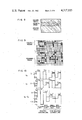
- FIG. 11 is a block diagram showing an embodiment of a driving device according to the present invention.
- FIG. 12 shows a detailed circuit configuration of an example of the scanning electrode driving circuit shown in FIG. 11.
- FIG. 13 shows voltage waveforms applied to liquid crystal cells in accordance with the present invention.
- FIG. 14 is a circuit diagram showing an example of the scanning signal generator shown in FIG. 11.
- FIGS. 3 and 4 which show a sectional view and a plan view of a matrix-type liquid crystal display panel, respectively two glass substrates 1 and 2 are superposed one upon the other with a spacer 3 interposed therebetween to provide a gap of about 10 ⁇ m.
- the gap is filled with a liquid crystal to form a liquid crystal layer 4.
- the glass substrates 1 and 2 are provided on the facing surfaces thereof with the stripes of transparent electrodes 5 and the stripes of transparent electrodes 6, respectively, and are arranged in such a manner that the electrodes 5 intersect the electrodes 6 at right angles, to form a matrix structure. That is, a liquid crystal cell 7 is formed at each of intersecting points between the electrodes 5 and the electrodes 6, as is indicated by an equivalent circuit shown in FIG. 5.
- Such a matrix-type liquid crystal display panel is usually driven with the one-line-at-a-time scanning system.
- a chiral-nematic liquid crystal was made by adding an optically active material, for example, CB-15 having a constitutional formula ##STR1## in a concentration of 2 to 5% by weight, to a nematic liquid crystal, for example, to ZLI-1132 (cyclohexane type) manufactured by the Merck Co.
- FIG. 1 is a graph in a case where a dark character or pattern is displayed against a light background
- FIG. 6 is a graph in a case where a light character or pattern is displayed against a dark background. Therefore, the graph of FIG. 1 is reversed in form of characteristic curve as compared with that of FIG. 6.
- the following operation is preferable since a low voltage drive can be conducted.
- the liquid crystal cells are first applied with a holding voltage V NS , and are thereby brought in an initial state "L S ".
- L S holding voltage
- the selected points are applied with a write-in voltage V S , and are thereby put in a state "W” of high brightness.
- the selected points are applied with the holding voltage V NS to be kept in a state indicated by "H S ". That is, a character or picture image is displayed by two states, namely, the state "L S " of low brightness and the state "H S " of high brightness.
- FIG. 7 shows the waveforms of voltages applied to liquid crystal cells in a case where a liquid crystal panel having five scanning lines is scanned with the one-line-at-a-time scanning system and is driven in the amplitude selective multiplexing method.
- FIG. 7(a) shows the waveform of voltage applied to a selected liquid crystal cell
- FIG. 7(b) the waveform of voltage applied to a half-selected point where only the row electrode is selected
- FIG. 7(c) the waveform of voltage applied to another half-selected point where only the column electrode is selected.
- FIG. 7 is concerned with a case that the panel includes five scanning lines.
- the panel includes N scanning lines.
- the root mean square value at one period of a waveform such as shown in FIG. 7(a), that is, a write-in voltage V S is given by the following equation: ##EQU1## where a indicates a bias ratio equal to or greater than 2.
- the root mean square value of a waveform applied to a half-selected point (where only the scanning line is selected), that is, a holding voltage V NS is given by the following equation: ##EQU2## Further, the root mean square value of a waveform applied to another half-selected point (where only the column electrode is selected), that is, another holding voltage V H is expressed by the following relation: ##EQU3##
- the write-in voltage V S is greater than the holding voltage V NS , and the ratio of V S to V NS is given by the following equation: ##EQU4##
- the bias ratio a is equal to ( ⁇ N+1)
- the above ratio assumes a maximum value given by the following equation: ##EQU5##
- the voltage ratio V S /V NS is decreased and approximates to 1 (one), as the number of scanning lines is greater.
- the write-in voltage V S and the holding voltage V NS assume nearly the same value, and therefore the point W shown in FIG. 6 is brought close to the point L S .
- the point W cannot be placed in a saturation region, and therefore the contrast of displayed images is lowered.
- a large-scale matrix-type liquid crystal display panel is divided into two kinds of regions, namely, the scanning region where the writing operation is presently being conducted and the holding region where the display state is maintained as it is.
- the scanning region is scanned with the one-line-at-a-time scanning system, and one or more holding regions are applied with a holding voltage to maintain a display state as it is.
- the voltage ratio V S /V NS equal to ⁇ 2 is obtainable, as is known from equation (5), and therefore the display panel can exhibit a high contrast.
- one of the holding regions becomes the scanning region where the one-line-at-a-time scanning operation is repeatedly performed to write information in this region.
- FIG. 9 shows, in part, the display plane of a display panel which is divided into a plurality of character rows each capable of including a series of characters arranged in the direction of scanning line.
- each of the character rows is used as the scanning region, and the rows are successively scanned to write characters in the whole display plane. That is, other character rows than that just scanned make up the holding region.
- FIG. 10 shows, in waveform per cycle, voltages for driving the above display panel in the amplitude selective multiplexing method, which voltages are applied to selected, half-selected and non-selected points.
- a voltage V X applied to each row electrode assumes a waveform V XS when the electrode is selected and assumes a waveform V XNS when non-selected
- a voltage V Y applied to each column electrode assumes a waveform V YS or V YNS according as the electrode is selected or not.
- a voltage V X -V Y applied to a liquid crystal cell assumes waveforms V S ', V NS ', V NS " and V NS '" for a selected cell, a half-selected cell on the selected scanning line (or a half-selected cell along the selected row electrode), a half-selected cell on the non-selected scanning line and a non-selected cell, respectively.
- the waveform V S ' is applied to the selected cell for only one fifth of the scanning period, as is known from FIG. 7(a).
- the selected cell is applied with the waveform V NS " for the remaining period to be put in the half-selected state.
- the half-selected cell in the scanning region which is not subjected to the write-in operation, is applied with the waveform V NS ' for one fifth of the scanning period and with the waveform V NS '" for the remaining period, as is shown in FIG. 7(b).
- the half-selected cell along the selected column electrode is continuously applied with the waveform V NS ", as is shown in FIG.
- the non-selected cell is continuously applied with the waveform V NS '".
- the voltage applied to the non-selected cell is reversed in polarity as compared with that applied to the half-selected cell along the selected column electrode.
- the half-selected cell in the scanning region which is not subjected to the write-in operation is applied with the voltage having the waveform shown in FIG. 7(b).
- the root mean square value of the above voltage is equal to the holding voltage V NS given by equation (2).
- the half-selected and non-selected cells in the holding region are then applied respectively with the waveform shown in FIG. 7(c) and the inverted waveform thereof.
- the root mean square values of these waveforms are both equal to the holding voltage V H given by equation (3).
- the holding voltage V NS is greater than the holding voltage V H . That is, two holding voltages are employed, as is shown in FIG. 6.
- the holding voltage V NS Since the holding voltage V NS is applied to the half-selected cell in the scanning region, the phase transition speed of the liquid crystal used becomes high as the difference between the holding voltage V NS and the write-in voltage V S is smaller.
- the relative brightness of a liquid crystal cell at a time when the holding voltage V NS is applied is not always coincident with that at a time when the holding voltage V H is applied. Accordingly, the whole display plane becomes irregular in brightness, so that a flicker is generated on the display plane.
- the above problem can be solved in the following manner. As mentioned previously, the liquid crystal cells in the holding retion are always applied with the holding voltage V H . Accordingly, if the waveform V NS ' shown in FIG.
- the applied voltage is temporarily made equal to zero to translate all the liquid crystal cells from the state of "H S " or "H h “ to the state of "L S " or "L h ".
- a matrix-type liquid crystal display panel 11 includes row electrodes, column electrodes and a liquid crystal layer sandwiched therebetween.
- the row electrodes and the column electrodes are arranged so as to form a matrix structure.
- the display plane of the panel 11 is divided into a plurality of display regions (or scanning blocks) each including a plurality of scanning electrodes (or row electrodes).
- Scanning electrode driving circuits 12a to 12n are provided in correspondence to the display regions, and each of the circuits 12a to 12n drives the scanning electrodes included in a corresponding display region.
- Scanning signals are supplied in parallel from a scanning signal generator 13 to each of the scanning electrode driving circuits 12a to 12n through signal lines, the number of which is equal to the number of scanning electrodes included in one display region.
- the signal lines are successively applied with a high-level signal to cause each of the driving circuit 12a to 12n to perform the one-line-at-a-time scanning operation.
- a scanning block control circuit 14 selects one of the scanning electrode driving circuits 12a to 12n which is to be scanned, and then selects a next scanning electrode driving circuit when the scanning operation in the preceding driving circuit has been completed, in order to perform the scanning operation in the next scanning electrode driving circuit.
- Such an operation of the scanning block control circuit 14 is repeated to perform the scanning operation in all of the scanning electrode driving circuits 12a to 12n.
- the above selection is made by applying a high-level signal to a signal line which is connected to a scanning electrode driving circuit to be scanned.
- a voltage generator 15 generates the voltages having the waveforms V XS , V XNS , V YS and V YNS shown in FIG. 10.
- Each of the scanning electrode driving circuits 12a to 12n is supplied with the selection voltage (or voltage waveform) V XS and the non-selection voltage (or voltage waveform) V XNS from the voltage generator 15, and is further supplied with the scanning signals from the scanning signal generator 13 when applied with the high-level signal from the scanning block control circuit 14.
- the scanning electrode driving circuit is applied with the low-level signal from the scanning block control circuit 14
- the scanning signal which is supplied from the scanning signal generator 13 to the scanning electrode driving circuit, is blocked, that is, put in the low level.
- This operation can be conducted by providing AND gates 16a to 16m, which are controlled by a signal from the scanning block control circuit 14, respectively on m signal lines for connecting the scanning signal generator 13 to one of the scanning electrode driving circuits, as is shown in FIG.
- the voltages V XS and V XNS are applied to the scanning electrodes through switching circuits 17a to 17m and switching circuits 18a to 18m.
- the number of AND gates 16a to 16m, that of switching circuits 17a to 17m and that of switching circuits 18a to 18m are all equal to the number of scanning electrodes included in one display region (or scanning block).
- the switching circuits 17a to 17m and 18a to 18m are controlled by the output signals of the AND gates 16a to 16m in the following manner.
- the switching circuits 17a and 18a are applied with a high-level signal from a corresponding AND gate, namely, the AND gate 16a, the switching circuits 17a and 18a are operated so as to apply the voltage V XS to a corresponding scanning electrode. While, when applied with a low-level signal from the AND gate 16a, the switching circuits 17a and 18a are operated so as to apply the voltage V XNS to the corresponding scanning electrode.
- a timing circuit 20 includes therein a plurality of cascade-connected frequency dividers, which successively divide the frequency of a pulse train from a clock signal generator 21 to send out desired timing signals. Since the frequency dividers have the same structure as the counters, the address of a refresh memory 22 can be formed by the contents of a frequency devider.
- the refresh memory 22 stores therein information, which is to be displayed on the display plane, in the form of code. The stored information is read out in accordance with an address signal from the timing circuit 20, and is then sent as display information to a display pattern generator 23.
- the display pattern generator 23 generates a video signal on the basis of the display information to send the video signal to a shift register 24.
- the shift register 24 effects the series-parallel conversion for the video signal in accordance with an instruction from the timing circuit 20.
- the converted video signal is sent to a line memory 26 through signal lines, which correspond to the column electrodes of the display panel 11. Since the relation in operation among the refresh memory 22, display pattern generator 23 and shift register 24 is well known, the detail explanation thereof is omitted for the sake of simplicity.
- a column electrode driving circuit 27 has the same circuit construction as that part of the circuit shown in FIG. 12 which includes the switching circuits 17a to 17m and the switching circuits 18a to 18m.
- the selection voltage V YS is applied to a column electrode correspoiding to the output line of the line memory 26 applied with a high-level signal
- the non-selection voltage V YNS is applied to a column electrode corresponding to the output line applied with a low-level signal.
- the timing circuit 20 delivers on an output line 30 a control pulse which is synchronized with a time at which a scanning electrode is selected.
- the control pulse may have the duty of 50%.
- the scanning signal generator 13 successively delivers the scanning signal on the output lines thereof in synchronism with the control pulse.
- the voltage generator 15 delivers the selection voltage V XS and V YS and the non-selection voltages V XNS and V YNS in synchronism with the control pulse.
- the refresh memory 22 sends out information in synchronism with the control pulse. Further, the line memory 26 takes in the video signal in synchronism with the control pulse.
- the scanning block control circuit 14 is controlled by another pulse from the timing circuit 20.
- FIG. 13 shows the waveforms of voltages applied to liquid crystal cells by the above-mentioned circuit arrangement, in a case where each of the scanning electrode driving circuits 12a to 12n drives five row electrodes.
- the driving circuit 12a scans first, second, third, fourth and fifth scanning electrodes in the one-line-at-a-time scanning method. These five electrodes are successively applied with the selection voltage in one scanning period.
- liquid crystal cells which are sandwiched between the first, second, third, fourth and fifth scanning electrodes and a selected column electrode, are applied with the voltage waveforms indicated by solid lines in FIG. 13.
- liquid crystal cells which are sandwiched between the above scanning electrodes and a non-selected column electrode, are applied with the voltage waveforms indicated by broken lines in FIG. 13.
- the one-line-at-a-time scanning operation is performed once in a period from t 1 to t 1 ", and a second scanning electrode driving circuit 12b is selected at a time t 2 .
- the row electrodes, and column electrodes which are concerned with all the liquid crystal cells contained in the holding region, are applied respectively with the selection voltage and the non-selection voltage once in one period of one-line-at-a-time scanning operation, in order to avoid irregularity of brightness or flicker on the display plane. As shown in FIG. 13, this is done in the last cycle of each one-line-at-a-time scanning period, for example, at time intervals from t 1 ' to t 1 " and from t 2 ' to t 2 ".
- the outputs of the scanning block control circuit 14 are inverted in polarity to apply a low-level signal to a selected scanning electrode driving circuit and to apply a high-level signal to each of the remaining scanning electrode driving circuits, and all the output lines of the scanning signal generator 13 are applied with high-level signals.
- FIG. 14 shows a circuit arrangement of the scanning signal generator 13 which can effect the above operation. Referring to FIG. 13, the output lines of a ring counter 32 are successively put in the state of "HIGH" in response to the control pulse. As a result, the output lines of the scanning signal generator 13 are successively applied with a high-level signal through AND gates 33a to 33m and OR gates 34a to 34m.
Abstract
A driving device for a matrix-type display panel using a guest-host type liquid crystal made by adding a pleochroic dye to a nematic-cholesteric phase transition liquid crystal or a chiralnematic phase transition liquid crystal is disclosed in which the display plane of a display panel is divided into a plurality of blocks in such a manner that each block includes a plurality of scanning lines, that is, a plurality of regions are formed, only one of the regions is selected to be used a scanning region, the one-line-at-a-time scanning operation is repeated many times in the scanning region in order to write and display information to perfection, and the regions are selected successively and cyclically to be used as the scanning region.
Description
The present invention relates to a device for driving a guest-host type liquid crystal which is made by adding a pleochroic dye to a nematic-cholesteric phase transition liquid crystal or a chiralnematic phase transition liquid crystal, and more particularly to a driving device for a matrix-type display panel making use of a holding effect of the guest-host type liquid crystal.
Such phase transition liquid crystals as above exhibit a hysteresis phenomenon between the relative brightness thereof and the root mean square value of a voltage applied thereto. This hysteresis phenomenon is referred to as the holding effect, which is utilized as follows. Each liquid crystal cell is first applied with a holding voltage having a voltage value which is intermediate between the rising and falling voltages of a hysteresis loop, and a desired cell is then applied with a write-in voltage to be subjected to a phase transition. When the voltage applied to the desired cell is restored to the original holding voltage, the cell is maintained as it is. In other words, these liquid crystals, as is shown in FIG. 1 of the accompanying drawings, can assume at the holding voltage two stable states, in one of which the cell is put in the focalconic phase and scatters light, and in the other state, the cell is put in the nematic phase and becomes transparent. Therefore, it becomes possible by making use of the above hysteresis phenomenon to display a picture image, to increase a phase transition speed, and to prolong a memory time (holding time).
A conventional device for driving a matrix-type liquid crystal display panel, which makes use of the holding effect of the phase transition liquid crystals, is disclosed in an article entitled "Pulse-Length Modulation Achieves Two-Phase Writing in Matrix-Addressed Liquid Crystal Information Displays", by K. H. Walter and M. K. Taner, IEEE Transactions on Electron Devices, Vol. ED-25, No. 2, February 1978, pp. 172 to 174. In this method, a two-phase operation is employed, and each of the holding (sustaining), the write-in and the erasing voltages is formed through pulse-length modulation. In more detail, as is shown in FIG. 2, a voltage VH having a root mean square value Vo √1/N (where Vo indicates a peak value, and N the number of scanning lines) is used as the holding voltage. Further, in writing operation, a selected point is applied with a voltage Vs having a root means square value Vo √2/N to assume the focalconic phase, and a non-selected point is applied with VNS equal to OV to assume the nematic phase. Furthermore, a voltage VE having a high root mean square value Vo √(1-1/N) is used to erase information. As is evident from the above, the ratio of the voltage Vs applied to the selected point in the writing operation to the holding voltage VH (VS /VH) is equal to √2. Since the ratio VS /VH is fixed as above, it is impossible to set the contrast of picture image to an optimal value by appropriately selecting the ratio VS /VH in accordance with the characteristic of a liquid crystal cell used. Further, when the display panel becomes large-sized and the number of scanning lines is increased, the addressing time has to be reduced. In such a case, according to the above method, it is required to employ a high peak value Vo, and therefore it is impossible to drive the display panel by a low voltage circuit using a complementary MOS large scale integration (CMOSLSI).
Further, in a case where a large number of scanning lines are employed in a matrix-type liquid crystal display device, there appears the flicker on a display plane even when the display device is driven with a one-line-at-a-time scanning system, since the liquid crystal is generally slow in response speed. In order to prevent the above flicker, a rapid scanning mode for displaying a picture image has been employed in which the one-line-at-a-time scanning is repeatedly conducted to reduce the flicker by virtue of accumulative response effect. The rapid scanning mode is generally employed together with an amplitude selective multiplexing method, for the purpose of avoiding crosstalk, as is described in a U.S. Pat. No. 3,976,362. In this driving method, however, the number of scanning lines cannot exceed a limit, since the flicker is generated when the frame frequency of the one-line-at-a-time scanning is decreased to a value because of an increase in number of scanning lines, and since it is not possible to make the peak value of the voltage applied to the liquid crystal larger than a value for the purpose of enhancing the frame frequency.
An object of the present invention is to provide a driving device for a matrix-type display panel using a guest-host type phase transition liquid crystal which can increase the number of scanning lines without reducing the contrast ratio of displayed images.
According to the present invention which attains the above object, a matrix-type liquid crystal display panel including a guest-host type liquid crystal which is made by adding a pleochroic dye to a nematiccholesteric phase transition liquid crystal or a chiralnematic phase transition liquid crystal, is employed to make use of the holding effect of the guest-host type liquid crystal, and the display panel is divided into a holding region for holding a display state and a scanning region in which a display pattern is written, to drive these regions separately. Further, the holding region is applied with a holding voltage.
FIG. 1 is a graph which shows a relation between the applied voltage and the contrast ratio, and is described in a prior publication.
FIG. 2 shows pulse waveforms for driving a matrix-type liquid crystal display panel which are disclosed in the prior publication.
FIG. 3 is a sectional view for showing the construction of a matrix-type liquid crystal display panel to which the present invention is applied.
FIG. 4 is a plan view of the matrix-type liquid crystal display panel shown in FIG. 3.
FIG. 5 shows an equivalent circuit of the matrix-type liquid crystal display panel shown in FIGS. 3 and 4.
FIG. 6 is a graph showing a relation between the voltage applied to a liquid crystal used in the present invention and the relative brightness of the liquid crystal.
FIG. 7, including a-c, shows the waveforms of driving voltages applied to selected, half-selected and non-selected points of a matrix-type liquid crystal display panel.
FIGS. 8 and 9 show how a display plane is divided into a plurality of regions in accordance with the present invention.
FIG. 10 shows the waveforms per cycle of voltages VX, VY and VX -VY which are applied respectively to row electrodes, column electrodes and liquid crystal cells of a matrix-type liquid crystal display panel in accordance with the present invention.
FIG. 11 is a block diagram showing an embodiment of a driving device according to the present invention.
FIG. 12 shows a detailed circuit configuration of an example of the scanning electrode driving circuit shown in FIG. 11.
FIG. 13 shows voltage waveforms applied to liquid crystal cells in accordance with the present invention.
FIG. 14 is a circuit diagram showing an example of the scanning signal generator shown in FIG. 11.
Referring to FIGS. 3 and 4 which show a sectional view and a plan view of a matrix-type liquid crystal display panel, respectively two glass substrates 1 and 2 are superposed one upon the other with a spacer 3 interposed therebetween to provide a gap of about 10 μm. The gap is filled with a liquid crystal to form a liquid crystal layer 4. Further, the glass substrates 1 and 2 are provided on the facing surfaces thereof with the stripes of transparent electrodes 5 and the stripes of transparent electrodes 6, respectively, and are arranged in such a manner that the electrodes 5 intersect the electrodes 6 at right angles, to form a matrix structure. That is, a liquid crystal cell 7 is formed at each of intersecting points between the electrodes 5 and the electrodes 6, as is indicated by an equivalent circuit shown in FIG. 5. Such a matrix-type liquid crystal display panel is usually driven with the one-line-at-a-time scanning system.
The inventors studied the property of a guest-host type liquid crystal in which a pleochroic dye was added to a nematic-cholesteric phase transition liquid crystal or a chiralnematic phase transition liquid crystal, using the above-mentioned display panel, and found that the guest-host type liquid crystal exhibited a remarkable holding effect. In more detail, a chiral-nematic liquid crystal was made by adding an optically active material, for example, CB-15 having a constitutional formula ##STR1## in a concentration of 2 to 5% by weight, to a nematic liquid crystal, for example, to ZLI-1132 (cyclohexane type) manufactured by the Merck Co. Further, a pleochroic cyanine dye NK-2233 (blue) was added in a concentration of 1% by weight to the above chiralnematic liquid crystal to obtain a guest-host type liquid crystal. The electro-optical characteristic of the display panel containing the guest-host type liquid crystal was measured, and it was found that the relative brightness of the liquid crystal exhibited, as shown in FIG. 6, a hysteresis against the applied voltage. In other words, the relative brightness depends upon the root mean square value of applied voltage, and the locus of the relative brightness at the rising time of voltage is different from that at the falling time. Incidentally, FIG. 1 is a graph in a case where a dark character or pattern is displayed against a light background, and FIG. 6 is a graph in a case where a light character or pattern is displayed against a dark background. Therefore, the graph of FIG. 1 is reversed in form of characteristic curve as compared with that of FIG. 6.
In the driving methods making use of the characteristic shown in FIG. 6, the following operation is preferable since a low voltage drive can be conducted. The liquid crystal cells are first applied with a holding voltage VNS, and are thereby brought in an initial state "LS ". When information is written in the liquid crystal layer, only selected points (or selected liquid crystal cells) are applied with a write-in voltage VS, and are thereby put in a state "W" of high brightness. After the writing operation has been completed, the selected points are applied with the holding voltage VNS to be kept in a state indicated by "HS ". That is, a character or picture image is displayed by two states, namely, the state "LS " of low brightness and the state "HS " of high brightness.
In order to perform the above operation, the liquid crystal panel is driven in such an amplitude selective multiplexing method as mentioned below. FIG. 7 shows the waveforms of voltages applied to liquid crystal cells in a case where a liquid crystal panel having five scanning lines is scanned with the one-line-at-a-time scanning system and is driven in the amplitude selective multiplexing method. FIG. 7(a) shows the waveform of voltage applied to a selected liquid crystal cell, FIG. 7(b) the waveform of voltage applied to a half-selected point where only the row electrode is selected, and FIG. 7(c) the waveform of voltage applied to another half-selected point where only the column electrode is selected.
As mentioned above, FIG. 7 is concerned with a case that the panel includes five scanning lines. In order to treat a general case, however, let us assume that the panel includes N scanning lines. In this case, the root mean square value at one period of a waveform such as shown in FIG. 7(a), that is, a write-in voltage VS is given by the following equation: ##EQU1## where a indicates a bias ratio equal to or greater than 2. The root mean square value of a waveform applied to a half-selected point (where only the scanning line is selected), that is, a holding voltage VNS is given by the following equation: ##EQU2## Further, the root mean square value of a waveform applied to another half-selected point (where only the column electrode is selected), that is, another holding voltage VH is expressed by the following relation: ##EQU3##
As can be seen from equations (1) and (2), the write-in voltage VS is greater than the holding voltage VNS, and the ratio of VS to VNS is given by the following equation: ##EQU4## When the bias ratio a is equal to (√N+1), the above ratio assumes a maximum value given by the following equation: ##EQU5##
As is evident from equation (5), the voltage ratio VS /VNS is decreased and approximates to 1 (one), as the number of scanning lines is greater. In other words, the write-in voltage VS and the holding voltage VNS assume nearly the same value, and therefore the point W shown in FIG. 6 is brought close to the point LS. As a result, the point W cannot be placed in a saturation region, and therefore the contrast of displayed images is lowered.
In order to solve the above problem, according to the present invention, a large-scale matrix-type liquid crystal display panel, as shown in FIG. 8, is divided into two kinds of regions, namely, the scanning region where the writing operation is presently being conducted and the holding region where the display state is maintained as it is. In more detail, only the scanning region is scanned with the one-line-at-a-time scanning system, and one or more holding regions are applied with a holding voltage to maintain a display state as it is. For example, when the scanning region is set so as to include nine scanning lines, the voltage ratio VS /VNS equal to √2 is obtainable, as is known from equation (5), and therefore the display panel can exhibit a high contrast. After the write-in operation has been completed in one scanning region, one of the holding regions becomes the scanning region where the one-line-at-a-time scanning operation is repeatedly performed to write information in this region.
FIG. 9 shows, in part, the display plane of a display panel which is divided into a plurality of character rows each capable of including a series of characters arranged in the direction of scanning line. In this case, each of the character rows is used as the scanning region, and the rows are successively scanned to write characters in the whole display plane. That is, other character rows than that just scanned make up the holding region. FIG. 10 shows, in waveform per cycle, voltages for driving the above display panel in the amplitude selective multiplexing method, which voltages are applied to selected, half-selected and non-selected points. Referring to FIG. 10, a voltage VX applied to each row electrode (scanning electrode) assumes a waveform VXS when the electrode is selected and assumes a waveform VXNS when non-selected, and a voltage VY applied to each column electrode assumes a waveform VYS or VYNS according as the electrode is selected or not. Accordingly, a voltage VX -VY applied to a liquid crystal cell assumes waveforms VS ', VNS ', VNS " and VNS '" for a selected cell, a half-selected cell on the selected scanning line (or a half-selected cell along the selected row electrode), a half-selected cell on the non-selected scanning line and a non-selected cell, respectively.
In a case where the scanning region includes five scanning lines, the waveform VS ' is applied to the selected cell for only one fifth of the scanning period, as is known from FIG. 7(a). The selected cell is applied with the waveform VNS " for the remaining period to be put in the half-selected state. The half-selected cell in the scanning region which is not subjected to the write-in operation, is applied with the waveform VNS ' for one fifth of the scanning period and with the waveform VNS '" for the remaining period, as is shown in FIG. 7(b). Further, in the holding region, the half-selected cell along the selected column electrode is continuously applied with the waveform VNS ", as is shown in FIG. 7(c), and the non-selected cell is continuously applied with the waveform VNS '". As is apparent from the waveforms VNS " and VNS '" shown in FIG. 10, the voltage applied to the non-selected cell is reversed in polarity as compared with that applied to the half-selected cell along the selected column electrode.
As has been mentioned above, the half-selected cell in the scanning region which is not subjected to the write-in operation, is applied with the voltage having the waveform shown in FIG. 7(b). The root mean square value of the above voltage is equal to the holding voltage VNS given by equation (2). The half-selected and non-selected cells in the holding region are then applied respectively with the waveform shown in FIG. 7(c) and the inverted waveform thereof. The root mean square values of these waveforms are both equal to the holding voltage VH given by equation (3). As is apparent from the comparison between equations (2) and (3), the holding voltage VNS is greater than the holding voltage VH. That is, two holding voltages are employed, as is shown in FIG. 6.
Since the holding voltage VNS is applied to the half-selected cell in the scanning region, the phase transition speed of the liquid crystal used becomes high as the difference between the holding voltage VNS and the write-in voltage VS is smaller. On the other hand, in this case, the relative brightness of a liquid crystal cell at a time when the holding voltage VNS is applied, is not always coincident with that at a time when the holding voltage VH is applied. Accordingly, the whole display plane becomes irregular in brightness, so that a flicker is generated on the display plane. The above problem can be solved in the following manner. As mentioned previously, the liquid crystal cells in the holding retion are always applied with the holding voltage VH. Accordingly, if the waveform VNS ' shown in FIG. 10 is applied to all the cells in the holding region every time the scanning region is scanned, the voltage applied to the cells in the holding region becomes equal to the voltage VNS, which is applied to the half-selected cell in the scanning region. That is, all of the liquid crystal cells of the display panel other than selected cells are applied with the same holding voltage VNS. Thus, the above-mentioned irregularity in brightness or the flicker may be prevented.
Further, when information written in the liquid crystal layer is erased, the applied voltage is temporarily made equal to zero to translate all the liquid crystal cells from the state of "HS " or "Hh " to the state of "LS " or "Lh ".
Next, explanation will be made on a driving circuit for a matrix-type liquid crystal display panel.
Referring to FIG. 11, a matrix-type liquid crystal display panel 11 includes row electrodes, column electrodes and a liquid crystal layer sandwiched therebetween. The row electrodes and the column electrodes are arranged so as to form a matrix structure. The display plane of the panel 11 is divided into a plurality of display regions (or scanning blocks) each including a plurality of scanning electrodes (or row electrodes). Scanning electrode driving circuits 12a to 12n are provided in correspondence to the display regions, and each of the circuits 12a to 12n drives the scanning electrodes included in a corresponding display region. Scanning signals are supplied in parallel from a scanning signal generator 13 to each of the scanning electrode driving circuits 12a to 12n through signal lines, the number of which is equal to the number of scanning electrodes included in one display region. The signal lines are successively applied with a high-level signal to cause each of the driving circuit 12a to 12n to perform the one-line-at-a-time scanning operation. A scanning block control circuit 14 selects one of the scanning electrode driving circuits 12a to 12n which is to be scanned, and then selects a next scanning electrode driving circuit when the scanning operation in the preceding driving circuit has been completed, in order to perform the scanning operation in the next scanning electrode driving circuit. Such an operation of the scanning block control circuit 14 is repeated to perform the scanning operation in all of the scanning electrode driving circuits 12a to 12n. The above selection is made by applying a high-level signal to a signal line which is connected to a scanning electrode driving circuit to be scanned. A voltage generator 15 generates the voltages having the waveforms VXS, VXNS, VYS and VYNS shown in FIG. 10.
Each of the scanning electrode driving circuits 12a to 12n is supplied with the selection voltage (or voltage waveform) VXS and the non-selection voltage (or voltage waveform) VXNS from the voltage generator 15, and is further supplied with the scanning signals from the scanning signal generator 13 when applied with the high-level signal from the scanning block control circuit 14. When the scanning electrode driving circuit is applied with the low-level signal from the scanning block control circuit 14, the scanning signal, which is supplied from the scanning signal generator 13 to the scanning electrode driving circuit, is blocked, that is, put in the low level. This operation can be conducted by providing AND gates 16a to 16m, which are controlled by a signal from the scanning block control circuit 14, respectively on m signal lines for connecting the scanning signal generator 13 to one of the scanning electrode driving circuits, as is shown in FIG. 12. Referring to FIG. 12, the voltages VXS and VXNS are applied to the scanning electrodes through switching circuits 17a to 17m and switching circuits 18a to 18m. The number of AND gates 16a to 16m, that of switching circuits 17a to 17m and that of switching circuits 18a to 18m are all equal to the number of scanning electrodes included in one display region (or scanning block). The switching circuits 17a to 17m and 18a to 18m are controlled by the output signals of the AND gates 16a to 16m in the following manner. That is, when a pair of switching circuits for example, the switching circuits 17a and 18a are applied with a high-level signal from a corresponding AND gate, namely, the AND gate 16a, the switching circuits 17a and 18a are operated so as to apply the voltage VXS to a corresponding scanning electrode. While, when applied with a low-level signal from the AND gate 16a, the switching circuits 17a and 18a are operated so as to apply the voltage VXNS to the corresponding scanning electrode.
A timing circuit 20 includes therein a plurality of cascade-connected frequency dividers, which successively divide the frequency of a pulse train from a clock signal generator 21 to send out desired timing signals. Since the frequency dividers have the same structure as the counters, the address of a refresh memory 22 can be formed by the contents of a frequency devider. The refresh memory 22 stores therein information, which is to be displayed on the display plane, in the form of code. The stored information is read out in accordance with an address signal from the timing circuit 20, and is then sent as display information to a display pattern generator 23. The display pattern generator 23 generates a video signal on the basis of the display information to send the video signal to a shift register 24. The shift register 24 effects the series-parallel conversion for the video signal in accordance with an instruction from the timing circuit 20. The converted video signal is sent to a line memory 26 through signal lines, which correspond to the column electrodes of the display panel 11. Since the relation in operation among the refresh memory 22, display pattern generator 23 and shift register 24 is well known, the detail explanation thereof is omitted for the sake of simplicity. A column electrode driving circuit 27 has the same circuit construction as that part of the circuit shown in FIG. 12 which includes the switching circuits 17a to 17m and the switching circuits 18a to 18m. Accordingly, the selection voltage VYS is applied to a column electrode correspoiding to the output line of the line memory 26 applied with a high-level signal, and the non-selection voltage VYNS is applied to a column electrode corresponding to the output line applied with a low-level signal.
The timing circuit 20 delivers on an output line 30 a control pulse which is synchronized with a time at which a scanning electrode is selected. The control pulse may have the duty of 50%. The scanning signal generator 13 successively delivers the scanning signal on the output lines thereof in synchronism with the control pulse. The voltage generator 15 delivers the selection voltage VXS and VYS and the non-selection voltages VXNS and VYNS in synchronism with the control pulse. The refresh memory 22 sends out information in synchronism with the control pulse. Further, the line memory 26 takes in the video signal in synchronism with the control pulse. The scanning block control circuit 14 is controlled by another pulse from the timing circuit 20.
FIG. 13 shows the waveforms of voltages applied to liquid crystal cells by the above-mentioned circuit arrangement, in a case where each of the scanning electrode driving circuits 12a to 12n drives five row electrodes. Now, let us consider a case when the scanning block control circuit 14 selects the scanning electrode driving circuit 12a. The driving circuit 12a scans first, second, third, fourth and fifth scanning electrodes in the one-line-at-a-time scanning method. These five electrodes are successively applied with the selection voltage in one scanning period. Thus, liquid crystal cells which are sandwiched between the first, second, third, fourth and fifth scanning electrodes and a selected column electrode, are applied with the voltage waveforms indicated by solid lines in FIG. 13. On the other hand, liquid crystal cells which are sandwiched between the above scanning electrodes and a non-selected column electrode, are applied with the voltage waveforms indicated by broken lines in FIG. 13. The one-line-at-a-time scanning operation is performed once in a period from t1 to t1 ", and a second scanning electrode driving circuit 12b is selected at a time t2.
According to an embodiment of the present invention, the row electrodes, and column electrodes, which are concerned with all the liquid crystal cells contained in the holding region, are applied respectively with the selection voltage and the non-selection voltage once in one period of one-line-at-a-time scanning operation, in order to avoid irregularity of brightness or flicker on the display plane. As shown in FIG. 13, this is done in the last cycle of each one-line-at-a-time scanning period, for example, at time intervals from t1 ' to t1 " and from t2 ' to t2 ". In more detail, at these time intervals, the outputs of the scanning block control circuit 14 are inverted in polarity to apply a low-level signal to a selected scanning electrode driving circuit and to apply a high-level signal to each of the remaining scanning electrode driving circuits, and all the output lines of the scanning signal generator 13 are applied with high-level signals. FIG. 14 shows a circuit arrangement of the scanning signal generator 13 which can effect the above operation. Referring to FIG. 13, the output lines of a ring counter 32 are successively put in the state of "HIGH" in response to the control pulse. As a result, the output lines of the scanning signal generator 13 are successively applied with a high-level signal through AND gates 33a to 33m and OR gates 34a to 34m. However, when an output line 35 of the ring counter 32 is put in the state "HIGH", all the output lines of the scanning signal generator 13 are simultaneously applied with the high-level signal through an AND gate 36 and the OR gates 34a to 34m. The high-level signal from the AND gate 36 is also applied to the scanning block control circuit 14 to invert the polarity of every output thereof. Since a circuit for effecting the above inversion of polarity is well known, a circuit diagram thereof is omitted for brevity's sake.
Claims (5)
1. A driving device for a matrix-type display panel using a guest-host type phase transition liquid crystal comprising:
a matrix-type display panel including a guest-host type liquid crystal, said guest-host type crystal being made by adding a pleochroic dye to either one of a nematic-cholesteric phase transition liquid crystal and a chiralnematic phase transition liquid crystal;
a scanning region selecting circuit for selecting a scanning region on a display plane of said matrix-type display panel, said selected scanning region including a predetermined number of scanning lines, and being scanned to write information therein, said scanning region selecting circuit selecting a next scanning region when the scanning operation in said selected scanning region has been completed, so that said scanning region selecting circuit divides said matrix into said scanning region in which new information can be written and at least one holding region wherein new information cannot be written;
a scanning circuit for repeatedly scanning said scanning lines of said selected scanning region in a one-line-at-a-time scanning fashion, said scanning operation being repeated a plurality of times to write and display said information in full degree;
a scanning line voltage applying circuit for applying a desired selection voltage and a non-selection voltage respectively to a selected scanning line and all other scanning lines than said selected scanning lines, in synchronism with said one-line-at-a-time scanning operation performed by said scanning circuit;
a column voltage applying circuit for applying another selection voltage and another non-selection voltage respectively to one or more column electrodes and the remaining column electrodes in synchronism with said one-line-at-a-time scanning operation performed by said scanning circuit, said one or more column electrodes corresponding to one or more selected positions on said selected scanning line, all of said column electrodes being arranged perpendicular to said scanning lines; and
a voltage generator for supplying said scanning line voltage applying circuit with said selection and non-selection voltages and for supplying said column voltage applying circuit with said another selection and non-selection voltages,
wherein said respective selection and non-selection voltages applied to said scanning region serve to provide write-in signals for writing in new information to said scanning region, and wherein said respective selection and non-selection voltages applied to said holding region serve as holding signals to said holding region to maintain the display state of said holding region as it is.
2. A driving device for a matrix-type display panel using a guest-host type phase transition liquid crystal according to claim 1, wherein said scanning region selecting circuit includes a plurality of scanning line driving circuit corresponding to a plurality of divided regions of said display plane and a scanning block selecting circuit for selecting another scanning line driving circuit every time said scanning operation for writing information has been completed in one scanning line driving circuit and for effecting said selecting operation successively and repeatedly.
3. A driving device for a matrix-type display panel using a guest-host type phase transition liquid crystal according to claim 1 or 2, wherein said selection and non-selection voltages applied to said scanning lines and said another selection and non-selection voltages applied to said column electrodes have such waveforms as to apply a holding voltage ##EQU6## to those liquid crystal cells in said scanning region which are to be applied with a holding voltage, and to apply another holding voltage (1/a)Vo to all liquid crystal cells in other regions than said scanning region, where Vo, N and a indicate a peak value of voltage applied to selected liquid crystal cell, the number of scanning lines included in a scanning region, and a bias ratio, respectively.
4. A driving device for a matrix-type display panel using a guest-host type phase transition liquid crystal according to claim 3, wherein, at a time interval in one period of said one-line-at-a-time scanning operation conducted by said scanning circuit, said scanning line voltage applying circuit applies said selection voltage to each of scanning lines in other regions than said scanning region, and said column voltage applying circuit applies said another non-selection voltage to each of said column electrodes.
5. A driving device for a matrix-type display panel according to claim 2, wherein said scanning region selecting circuit includes gate means coupled between said scanning circuit and said scanning line driving circuits, said gate means being controlled by said scanning block selecting circuit to only passing a scanning signal from said scanning circuit to a selected scanning line driving circuit.
Applications Claiming Priority (2)
| Application Number | Priority Date | Filing Date | Title |
|---|---|---|---|
| JP14915378A JPS5576393A (en) | 1978-12-04 | 1978-12-04 | Matrix drive method for guestthostttype phase transfer liquid crystal |
| JP53-149153 | 1978-12-04 |
Publications (1)
| Publication Number | Publication Date |
|---|---|
| US4317115A true US4317115A (en) | 1982-02-23 |
Family
ID=15468931
Family Applications (1)
| Application Number | Title | Priority Date | Filing Date |
|---|---|---|---|
| US06/098,666 Expired - Lifetime US4317115A (en) | 1978-12-04 | 1979-11-29 | Driving device for matrix-type display panel using guest-host type phase transition liquid crystal |
Country Status (2)
| Country | Link |
|---|---|
| US (1) | US4317115A (en) |
| JP (1) | JPS5576393A (en) |
Cited By (66)
| Publication number | Priority date | Publication date | Assignee | Title |
|---|---|---|---|---|
| US4390872A (en) * | 1980-04-30 | 1983-06-28 | Reiji Murakami | Dot matrix condition display device for photocopiers |
| US4395709A (en) * | 1980-05-02 | 1983-07-26 | Hitachi, Ltd. | Driving device and method for matrix-type display panel using guest-host type phase transition liquid crystal |
| US4408201A (en) * | 1979-12-25 | 1983-10-04 | Kabushiki Kaisha Daini Seikosha | Electro-optic display device using phase transition mode liquid crystal |
| DE3235143A1 (en) * | 1982-09-23 | 1984-03-29 | BBC Aktiengesellschaft Brown, Boveri & Cie., 5401 Baden, Aargau | Method of driving a multiplexible bistable liquid-crystal display |
| EP0106386A2 (en) * | 1982-09-23 | 1984-04-25 | BBC Brown Boveri AG | Method of triggering a multiplexable bistable liquid crystal display |
| FR2542119A1 (en) * | 1982-12-28 | 1984-09-07 | Citizen Watch Co Ltd | METHOD FOR CONTROLLING A LIQUID CRYSTAL MATRIX DISPLAY SCREEN |
| FR2543341A1 (en) * | 1983-03-26 | 1984-09-28 | Citizen Watch Co Ltd | TELEVISION RECEIVER USING A LIQUID CRYSTAL MATRIX VIEWING SCREEN |
| EP0171177A2 (en) * | 1984-07-12 | 1986-02-12 | Northern Telecom Europe Limited | Addressing smectic displays |
| US4571585A (en) * | 1983-03-17 | 1986-02-18 | General Electric Company | Matrix addressing of cholesteric liquid crystal display |
| EP0171547A2 (en) * | 1984-07-13 | 1986-02-19 | Ascii Corporation | Display control system |
| US4625204A (en) * | 1983-02-24 | 1986-11-25 | Commissariat A L'energie Atomique | Sequential control process for a matrix display |
| EP0216188A2 (en) * | 1985-08-29 | 1987-04-01 | Canon Kabushiki Kaisha | Matrix display panel |
| US4688899A (en) * | 1984-07-27 | 1987-08-25 | Casio Computer Co., Ltd. | Dual-frequency, dielectric anisotropy liquid crystal display |
| US4701799A (en) * | 1984-03-13 | 1987-10-20 | Sharp Kabushiki Kaisha | Image display panel drive |
| US4702560A (en) * | 1984-10-11 | 1987-10-27 | Hitachi, Ltd. | Liquid crystal display device |
| US4714940A (en) * | 1983-08-16 | 1987-12-22 | Canon Kabushiki Kaisha | Image processing apparatus having display means to monitor and display information from a date input section |
| EP0256879A2 (en) * | 1986-08-18 | 1988-02-24 | Canon Kabushiki Kaisha | Display device |
| US4740786A (en) * | 1985-01-18 | 1988-04-26 | Apple Computer, Inc. | Apparatus for driving liquid crystal display |
| US4745485A (en) * | 1985-01-28 | 1988-05-17 | Sanyo Electric Co., Ltd | Picture display device |
| US4801933A (en) * | 1985-03-23 | 1989-01-31 | Sharp Kabushiki Kaisha | Liquid crystal matrix device having separate driving circuits with diverse driving voltages |
| EP0322071A2 (en) * | 1987-12-23 | 1989-06-28 | Koninklijke Philips Electronics N.V. | Neural network with dynamic refresh capability |
| US4844590A (en) * | 1985-05-25 | 1989-07-04 | Canon Kabushiki Kaisha | Method and apparatus for driving ferroelectric liquid crystal device |
| US4845473A (en) * | 1984-06-01 | 1989-07-04 | Sharp Kabushiki Kaisha | Method of driving a liquid crystal matrix display panel |
| US4923285A (en) * | 1985-04-22 | 1990-05-08 | Canon Kabushiki Kaisha | Drive apparatus having a temperature detector |
| WO1990012389A1 (en) * | 1989-04-04 | 1990-10-18 | Cirrus Logic, Inc. | Converter for raster-image data from single-segment to multi-segment streams |
| US4985698A (en) * | 1987-10-28 | 1991-01-15 | Hitachi, Ltd. | Display panel driving apparatus |
| US5012228A (en) * | 1987-08-04 | 1991-04-30 | Nippon Telegraph And Telephone | Method of operation for an active matrix type display device |
| US5028916A (en) * | 1984-09-28 | 1991-07-02 | Kabushiki Kaisha Toshiba | Active matrix display device |
| US5034736A (en) * | 1989-08-14 | 1991-07-23 | Polaroid Corporation | Bistable display with permuted excitation |
| EP0499101A2 (en) * | 1991-01-31 | 1992-08-19 | Hughes Aircraft Company | Shaped voltage pulse method for operating a polymer dispersed liquid crystal cell, and light valve employing the same |
| US5189535A (en) * | 1986-12-11 | 1993-02-23 | Fujitsu Limited | Liquid crystal display element and method for driving same |
| US5274484A (en) * | 1991-04-12 | 1993-12-28 | Fujitsu Limited | Gradation methods for driving phase transition liquid crystal using a holding signal |
| US5296953A (en) * | 1984-01-23 | 1994-03-22 | Canon Kabushiki Kaisha | Driving method for ferro-electric liquid crystal optical modulation device |
| US5298913A (en) * | 1987-05-29 | 1994-03-29 | Sharp Kabushiki Kaisha | Ferroelectric liquid crystal display device and driving system thereof for driving the display by an integrated scanning method |
| US5420604A (en) * | 1991-04-01 | 1995-05-30 | In Focus Systems, Inc. | LCD addressing system |
| US5430461A (en) * | 1993-08-26 | 1995-07-04 | Industrial Technology Research Institute | Transistor array for addressing display panel |
| US5642133A (en) * | 1991-04-01 | 1997-06-24 | In Focus Systems, Inc. | Split interval gray level addressing for LCDs |
| US5663745A (en) * | 1993-05-13 | 1997-09-02 | Casio Computer Co., Ltd. | Display driving device |
| US5689282A (en) * | 1991-07-09 | 1997-11-18 | U.S. Philips Corporation | Display device with compensation for stray capacitance |
| US5703616A (en) * | 1993-05-13 | 1997-12-30 | Casio Computer Co., Ltd. | Display driving device |
| US5739803A (en) * | 1994-01-24 | 1998-04-14 | Arithmos, Inc. | Electronic system for driving liquid crystal displays |
| US5748277A (en) * | 1995-02-17 | 1998-05-05 | Kent State University | Dynamic drive method and apparatus for a bistable liquid crystal display |
| US5764212A (en) * | 1994-02-21 | 1998-06-09 | Hitachi, Ltd. | Matrix type liquid crystal display device with data electrode driving circuit in which display information for one screen is written into and read out from display memory at mutually different frequencies |
| US5825346A (en) * | 1985-04-04 | 1998-10-20 | Seiko Precision Inc. | Method for driving electro-optical display device |
| US5896118A (en) * | 1988-10-31 | 1999-04-20 | Canon Kabushiki Kaisha | Display system |
| US5933203A (en) * | 1997-01-08 | 1999-08-03 | Advanced Display Systems, Inc. | Apparatus for and method of driving a cholesteric liquid crystal flat panel display |
| USRE36654E (en) * | 1989-03-28 | 2000-04-11 | In Focus Systems, Inc. | Stacked LCD color display |
| US6133895A (en) * | 1997-06-04 | 2000-10-17 | Kent Displays Incorporated | Cumulative drive scheme and method for a liquid crystal display |
| US6154190A (en) * | 1995-02-17 | 2000-11-28 | Kent State University | Dynamic drive methods and apparatus for a bistable liquid crystal display |
| US6204835B1 (en) | 1998-05-12 | 2001-03-20 | Kent State University | Cumulative two phase drive scheme for bistable cholesteric reflective displays |
| DE19723204C2 (en) * | 1996-06-07 | 2001-07-19 | Lg Semicon Co Ltd | Drive circuit for thin film transistor liquid crystal display |
| US6268840B1 (en) | 1997-05-12 | 2001-07-31 | Kent Displays Incorporated | Unipolar waveform drive method and apparatus for a bistable liquid crystal display |
| US6268839B1 (en) | 1998-05-12 | 2001-07-31 | Kent State University | Drive schemes for gray scale bistable cholesteric reflective displays |
| US6320563B1 (en) | 1999-01-21 | 2001-11-20 | Kent State University | Dual frequency cholesteric display and drive scheme |
| US20020080108A1 (en) * | 2000-12-26 | 2002-06-27 | Hannstar Display Corp. | Gate lines driving circuit and driving method |
| US20020154130A1 (en) * | 2001-04-18 | 2002-10-24 | Minoru Niimura | Liquid crystal display apparatus |
| WO2004066253A1 (en) * | 2003-01-23 | 2004-08-05 | Koninklijke Philips Electronics N.V. | Driving an electrophoretic display |
| US20050219190A1 (en) * | 2004-03-30 | 2005-10-06 | Dong Hoon Lee | Apparatus and method for driving liquid crystal display device |
| US7023409B2 (en) | 2001-02-09 | 2006-04-04 | Kent Displays, Incorporated | Drive schemes for gray scale bistable cholesteric reflective displays utilizing variable frequency pulses |
| US20060164380A1 (en) * | 2005-01-21 | 2006-07-27 | Hui-Wen Yang | Liquid crystal display and driving method thereof |
| US7126569B2 (en) * | 1999-03-23 | 2006-10-24 | Minolta Co., Ltd. | Liquid crystal display device |
| DE4428157B4 (en) * | 1993-08-09 | 2007-06-28 | Motorola, Inc., Schaumburg | Data receiver and method for its operation |
| DE4424521B4 (en) * | 1993-07-12 | 2007-07-12 | Motorola, Inc., Schaumburg | Electronic device for displaying data |
| CN100395813C (en) * | 2004-07-27 | 2008-06-18 | 精工爱普生株式会社 | Driving circuit and driving method of electro-optical device, electro-optical device, and electronic apparatus |
| CN103474044A (en) * | 2013-09-29 | 2013-12-25 | 北京京东方光电科技有限公司 | Grid driving circuit, array substrate, display device and driving method |
| WO2017088229A1 (en) * | 2015-11-26 | 2017-06-01 | 深圳市华星光电技术有限公司 | Display panel and array gate electrode driving circuit |
Citations (4)
| Publication number | Priority date | Publication date | Assignee | Title |
|---|---|---|---|---|
| US4100540A (en) * | 1975-11-18 | 1978-07-11 | Citizen Watch Co., Ltd. | Method of driving liquid crystal matrix display device to obtain maximum contrast and reduce power consumption |
| US4186395A (en) * | 1977-03-01 | 1980-01-29 | Kabushiki Kaisha Seikosha | Method of driving a liquid crystal display apparatus |
| US4200822A (en) * | 1978-05-15 | 1980-04-29 | Owens-Illinois, Inc. | MOS Circuit for generating a square wave form |
| US4203104A (en) * | 1977-07-29 | 1980-05-13 | Bbc Brown Boveri & Company Limited | Procedure of bargraph display for measured quantities |
-
1978
- 1978-12-04 JP JP14915378A patent/JPS5576393A/en active Pending
-
1979
- 1979-11-29 US US06/098,666 patent/US4317115A/en not_active Expired - Lifetime
Patent Citations (4)
| Publication number | Priority date | Publication date | Assignee | Title |
|---|---|---|---|---|
| US4100540A (en) * | 1975-11-18 | 1978-07-11 | Citizen Watch Co., Ltd. | Method of driving liquid crystal matrix display device to obtain maximum contrast and reduce power consumption |
| US4186395A (en) * | 1977-03-01 | 1980-01-29 | Kabushiki Kaisha Seikosha | Method of driving a liquid crystal display apparatus |
| US4203104A (en) * | 1977-07-29 | 1980-05-13 | Bbc Brown Boveri & Company Limited | Procedure of bargraph display for measured quantities |
| US4200822A (en) * | 1978-05-15 | 1980-04-29 | Owens-Illinois, Inc. | MOS Circuit for generating a square wave form |
Cited By (89)
| Publication number | Priority date | Publication date | Assignee | Title |
|---|---|---|---|---|
| US4408201A (en) * | 1979-12-25 | 1983-10-04 | Kabushiki Kaisha Daini Seikosha | Electro-optic display device using phase transition mode liquid crystal |
| US4390872A (en) * | 1980-04-30 | 1983-06-28 | Reiji Murakami | Dot matrix condition display device for photocopiers |
| US4395709A (en) * | 1980-05-02 | 1983-07-26 | Hitachi, Ltd. | Driving device and method for matrix-type display panel using guest-host type phase transition liquid crystal |
| DE3235143A1 (en) * | 1982-09-23 | 1984-03-29 | BBC Aktiengesellschaft Brown, Boveri & Cie., 5401 Baden, Aargau | Method of driving a multiplexible bistable liquid-crystal display |
| EP0106386A2 (en) * | 1982-09-23 | 1984-04-25 | BBC Brown Boveri AG | Method of triggering a multiplexable bistable liquid crystal display |
| EP0106386A3 (en) * | 1982-09-23 | 1985-03-13 | BBC Brown Boveri AG | Method of triggering a multiplexable bistable liquid crystal display |
| FR2542119A1 (en) * | 1982-12-28 | 1984-09-07 | Citizen Watch Co Ltd | METHOD FOR CONTROLLING A LIQUID CRYSTAL MATRIX DISPLAY SCREEN |
| US4625204A (en) * | 1983-02-24 | 1986-11-25 | Commissariat A L'energie Atomique | Sequential control process for a matrix display |
| US4571585A (en) * | 1983-03-17 | 1986-02-18 | General Electric Company | Matrix addressing of cholesteric liquid crystal display |
| FR2543341A1 (en) * | 1983-03-26 | 1984-09-28 | Citizen Watch Co Ltd | TELEVISION RECEIVER USING A LIQUID CRYSTAL MATRIX VIEWING SCREEN |
| US4714940A (en) * | 1983-08-16 | 1987-12-22 | Canon Kabushiki Kaisha | Image processing apparatus having display means to monitor and display information from a date input section |
| US5559616A (en) * | 1984-01-23 | 1996-09-24 | Canon Kabushiki Kaisha | Driving method for ferroelectric liquid crystal device with partial erasure and partial writing |
| US5296953A (en) * | 1984-01-23 | 1994-03-22 | Canon Kabushiki Kaisha | Driving method for ferro-electric liquid crystal optical modulation device |
| US4701799A (en) * | 1984-03-13 | 1987-10-20 | Sharp Kabushiki Kaisha | Image display panel drive |
| US4845473A (en) * | 1984-06-01 | 1989-07-04 | Sharp Kabushiki Kaisha | Method of driving a liquid crystal matrix display panel |
| EP0171177A3 (en) * | 1984-07-12 | 1987-04-29 | Northern Telecom Europe Limited | Addressing smectic displays |
| EP0171177A2 (en) * | 1984-07-12 | 1986-02-12 | Northern Telecom Europe Limited | Addressing smectic displays |
| EP0171547A3 (en) * | 1984-07-13 | 1988-09-07 | Ascii Corporation | Display control system |
| EP0171547A2 (en) * | 1984-07-13 | 1986-02-19 | Ascii Corporation | Display control system |
| US4688899A (en) * | 1984-07-27 | 1987-08-25 | Casio Computer Co., Ltd. | Dual-frequency, dielectric anisotropy liquid crystal display |
| US4832460A (en) * | 1984-07-27 | 1989-05-23 | Casio Computer Co., Ltd. | Liquid crystal apparatus having pressure absorbing means |
| US5028916A (en) * | 1984-09-28 | 1991-07-02 | Kabushiki Kaisha Toshiba | Active matrix display device |
| US4702560A (en) * | 1984-10-11 | 1987-10-27 | Hitachi, Ltd. | Liquid crystal display device |
| US4740786A (en) * | 1985-01-18 | 1988-04-26 | Apple Computer, Inc. | Apparatus for driving liquid crystal display |
| US4745485A (en) * | 1985-01-28 | 1988-05-17 | Sanyo Electric Co., Ltd | Picture display device |
| US4801933A (en) * | 1985-03-23 | 1989-01-31 | Sharp Kabushiki Kaisha | Liquid crystal matrix device having separate driving circuits with diverse driving voltages |
| US5825346A (en) * | 1985-04-04 | 1998-10-20 | Seiko Precision Inc. | Method for driving electro-optical display device |
| US4923285A (en) * | 1985-04-22 | 1990-05-08 | Canon Kabushiki Kaisha | Drive apparatus having a temperature detector |
| US4844590A (en) * | 1985-05-25 | 1989-07-04 | Canon Kabushiki Kaisha | Method and apparatus for driving ferroelectric liquid crystal device |
| EP0216188A3 (en) * | 1985-08-29 | 1989-04-05 | Canon Kabushiki Kaisha | Matrix display panel |
| EP0216188A2 (en) * | 1985-08-29 | 1987-04-01 | Canon Kabushiki Kaisha | Matrix display panel |
| EP0256879A2 (en) * | 1986-08-18 | 1988-02-24 | Canon Kabushiki Kaisha | Display device |
| US5952990A (en) * | 1986-08-18 | 1999-09-14 | Canon Kabushiki Kaisha | Display device with power-off delay circuitry |
| EP0256879A3 (en) * | 1986-08-18 | 1988-09-21 | Canon Kabushiki Kaisha | Display device |
| US6262705B1 (en) * | 1986-08-18 | 2001-07-17 | Canon Kabushiki Kaisha | Display device |
| US5189535A (en) * | 1986-12-11 | 1993-02-23 | Fujitsu Limited | Liquid crystal display element and method for driving same |
| US5298913A (en) * | 1987-05-29 | 1994-03-29 | Sharp Kabushiki Kaisha | Ferroelectric liquid crystal display device and driving system thereof for driving the display by an integrated scanning method |
| US5012228A (en) * | 1987-08-04 | 1991-04-30 | Nippon Telegraph And Telephone | Method of operation for an active matrix type display device |
| US4985698A (en) * | 1987-10-28 | 1991-01-15 | Hitachi, Ltd. | Display panel driving apparatus |
| EP0322071A2 (en) * | 1987-12-23 | 1989-06-28 | Koninklijke Philips Electronics N.V. | Neural network with dynamic refresh capability |
| EP0322071A3 (en) * | 1987-12-23 | 1990-03-14 | Koninklijke Philips Electronics N.V. | Neural network with dynamic refresh capability |
| US5896118A (en) * | 1988-10-31 | 1999-04-20 | Canon Kabushiki Kaisha | Display system |
| USRE36654E (en) * | 1989-03-28 | 2000-04-11 | In Focus Systems, Inc. | Stacked LCD color display |
| WO1990012389A1 (en) * | 1989-04-04 | 1990-10-18 | Cirrus Logic, Inc. | Converter for raster-image data from single-segment to multi-segment streams |
| US5034736A (en) * | 1989-08-14 | 1991-07-23 | Polaroid Corporation | Bistable display with permuted excitation |
| US5170271A (en) * | 1991-01-31 | 1992-12-08 | Hughes Aircraft Company | Shaped voltage pulse method for operating a polymer dispersed liquid crystal cell, and light valve employing the same |
| EP0499101A3 (en) * | 1991-01-31 | 1992-09-09 | Hughes Aircraft Company | Shaped voltage pulse method for operating a polymer dispersed liquid crystal cell, and light valve employing the same |
| EP0499101A2 (en) * | 1991-01-31 | 1992-08-19 | Hughes Aircraft Company | Shaped voltage pulse method for operating a polymer dispersed liquid crystal cell, and light valve employing the same |
| US5485173A (en) * | 1991-04-01 | 1996-01-16 | In Focus Systems, Inc. | LCD addressing system and method |
| US5642133A (en) * | 1991-04-01 | 1997-06-24 | In Focus Systems, Inc. | Split interval gray level addressing for LCDs |
| US5420604A (en) * | 1991-04-01 | 1995-05-30 | In Focus Systems, Inc. | LCD addressing system |
| US5585816A (en) * | 1991-04-01 | 1996-12-17 | In Focus Systems, Inc. | Displaying gray shades on display panel implemented with active addressing technique |
| US5852429A (en) * | 1991-04-01 | 1998-12-22 | In Focus Systems, Inc. | Displaying gray shades on display panel implemented with phase-displaced multiple row selections |
| US5546102A (en) * | 1991-04-01 | 1996-08-13 | In Focus Systems, Inc. | Integrated driver for display implemented with active addressing technique |
| US5274484A (en) * | 1991-04-12 | 1993-12-28 | Fujitsu Limited | Gradation methods for driving phase transition liquid crystal using a holding signal |
| US5689282A (en) * | 1991-07-09 | 1997-11-18 | U.S. Philips Corporation | Display device with compensation for stray capacitance |
| CN1044292C (en) * | 1993-05-13 | 1999-07-21 | 卡西欧计算机公司 | Display driving device |
| US5663745A (en) * | 1993-05-13 | 1997-09-02 | Casio Computer Co., Ltd. | Display driving device |
| US5703616A (en) * | 1993-05-13 | 1997-12-30 | Casio Computer Co., Ltd. | Display driving device |
| US5852428A (en) * | 1993-05-13 | 1998-12-22 | Casio Computer Co., Ltd. | Display driving device |
| DE4424521B4 (en) * | 1993-07-12 | 2007-07-12 | Motorola, Inc., Schaumburg | Electronic device for displaying data |
| DE4428157B4 (en) * | 1993-08-09 | 2007-06-28 | Motorola, Inc., Schaumburg | Data receiver and method for its operation |
| US5430461A (en) * | 1993-08-26 | 1995-07-04 | Industrial Technology Research Institute | Transistor array for addressing display panel |
| US5739803A (en) * | 1994-01-24 | 1998-04-14 | Arithmos, Inc. | Electronic system for driving liquid crystal displays |
| US5764212A (en) * | 1994-02-21 | 1998-06-09 | Hitachi, Ltd. | Matrix type liquid crystal display device with data electrode driving circuit in which display information for one screen is written into and read out from display memory at mutually different frequencies |
| US5748277A (en) * | 1995-02-17 | 1998-05-05 | Kent State University | Dynamic drive method and apparatus for a bistable liquid crystal display |
| US6154190A (en) * | 1995-02-17 | 2000-11-28 | Kent State University | Dynamic drive methods and apparatus for a bistable liquid crystal display |
| DE19723204C2 (en) * | 1996-06-07 | 2001-07-19 | Lg Semicon Co Ltd | Drive circuit for thin film transistor liquid crystal display |
| US5933203A (en) * | 1997-01-08 | 1999-08-03 | Advanced Display Systems, Inc. | Apparatus for and method of driving a cholesteric liquid crystal flat panel display |
| US6268840B1 (en) | 1997-05-12 | 2001-07-31 | Kent Displays Incorporated | Unipolar waveform drive method and apparatus for a bistable liquid crystal display |
| US6133895A (en) * | 1997-06-04 | 2000-10-17 | Kent Displays Incorporated | Cumulative drive scheme and method for a liquid crystal display |
| US6204835B1 (en) | 1998-05-12 | 2001-03-20 | Kent State University | Cumulative two phase drive scheme for bistable cholesteric reflective displays |
| US6268839B1 (en) | 1998-05-12 | 2001-07-31 | Kent State University | Drive schemes for gray scale bistable cholesteric reflective displays |
| US6320563B1 (en) | 1999-01-21 | 2001-11-20 | Kent State University | Dual frequency cholesteric display and drive scheme |
| US7126569B2 (en) * | 1999-03-23 | 2006-10-24 | Minolta Co., Ltd. | Liquid crystal display device |
| US6717566B2 (en) * | 2000-12-26 | 2004-04-06 | Hannstar Display Corp. | Gate lines driving circuit and driving method |
| US20020080108A1 (en) * | 2000-12-26 | 2002-06-27 | Hannstar Display Corp. | Gate lines driving circuit and driving method |
| US7023409B2 (en) | 2001-02-09 | 2006-04-04 | Kent Displays, Incorporated | Drive schemes for gray scale bistable cholesteric reflective displays utilizing variable frequency pulses |
| US20020154130A1 (en) * | 2001-04-18 | 2002-10-24 | Minoru Niimura | Liquid crystal display apparatus |
| US7116304B2 (en) * | 2001-04-18 | 2006-10-03 | Seiko Epson Corporation | Liquid crystal display apparatus |
| US20060132426A1 (en) * | 2003-01-23 | 2006-06-22 | Koninklijke Philips Electronics N.V. | Driving an electrophoretic display |
| WO2004066253A1 (en) * | 2003-01-23 | 2004-08-05 | Koninklijke Philips Electronics N.V. | Driving an electrophoretic display |
| US7688301B2 (en) * | 2004-03-30 | 2010-03-30 | Lg Display Co., Ltd. | Apparatus and method for driving liquid crystal display device |
| US20050219190A1 (en) * | 2004-03-30 | 2005-10-06 | Dong Hoon Lee | Apparatus and method for driving liquid crystal display device |
| CN100395813C (en) * | 2004-07-27 | 2008-06-18 | 精工爱普生株式会社 | Driving circuit and driving method of electro-optical device, electro-optical device, and electronic apparatus |
| US20060164380A1 (en) * | 2005-01-21 | 2006-07-27 | Hui-Wen Yang | Liquid crystal display and driving method thereof |
| US7696975B2 (en) * | 2005-01-21 | 2010-04-13 | Chi Mei Optoelectronics Corporation | Liquid crystal display having display blocks that display normal and compensation images |
| CN103474044A (en) * | 2013-09-29 | 2013-12-25 | 北京京东方光电科技有限公司 | Grid driving circuit, array substrate, display device and driving method |
| WO2017088229A1 (en) * | 2015-11-26 | 2017-06-01 | 深圳市华星光电技术有限公司 | Display panel and array gate electrode driving circuit |
Also Published As
| Publication number | Publication date |
|---|---|
| JPS5576393A (en) | 1980-06-09 |
Similar Documents
| Publication | Publication Date | Title |
|---|---|---|
| US4317115A (en) | Driving device for matrix-type display panel using guest-host type phase transition liquid crystal | |
| US4380008A (en) | Method of driving a matrix type phase transition liquid crystal display device to obtain a holding effect and improved response time for the erasing operation | |
| US4778260A (en) | Method and apparatus for driving optical modulation device | |
| JP3253481B2 (en) | Memory interface circuit | |
| US4395709A (en) | Driving device and method for matrix-type display panel using guest-host type phase transition liquid crystal | |
| JP3230755B2 (en) | Matrix driving method for flat display device | |
| EP0214857B1 (en) | Method of driving a liquid crystal matrix panel | |
| US6271819B1 (en) | Method for driving electro-optical display device | |
| JPS6238709B2 (en) | ||
| US20020000966A1 (en) | Liquid crystal display device | |
| JPH01133033A (en) | Liquid crystal display device and synthetic waveform generation circuit for driving the same | |
| US5353137A (en) | Liquid crystal apparatus | |
| JPH04204628A (en) | Liquid crystal display device | |
| EP0342835A1 (en) | Liquid crystal cell addressing | |
| JPH10325946A (en) | Optical modulation device | |
| US5614924A (en) | Ferroelectric liquid crystal display device and a driving method of effecting gradational display therefor | |
| JPH10268265A (en) | Liquid crystal display device | |
| US5748166A (en) | Addressing ferroelectric liquid crystal displays | |
| KR940010748A (en) | Driving method of strong dielectric liquid crystal panel | |
| JPH06301011A (en) | Matrix display device and its driving method | |
| JPH1069260A (en) | Method for driving nematic liquid crystal | |
| JPH02162322A (en) | Method for driving ferroelectric liquid crystal panel and driving controller | |
| JP2770981B2 (en) | Driving method of matrix type ferroelectric liquid crystal panel | |
| JPS6385523A (en) | Color electrooptic device by ferroelectric liquid crystal | |
| JP2717014B2 (en) | Driving method of display device |
Legal Events
| Date | Code | Title | Description |
|---|---|---|---|
| STCF | Information on status: patent grant |
Free format text: PATENTED CASE |