US4338281A - Thin film semiconductor gas sensor having an integrated heating element - Google Patents
Thin film semiconductor gas sensor having an integrated heating element Download PDFInfo
- Publication number
- US4338281A US4338281A US06/254,855 US25485581A US4338281A US 4338281 A US4338281 A US 4338281A US 25485581 A US25485581 A US 25485581A US 4338281 A US4338281 A US 4338281A
- Authority
- US
- United States
- Prior art keywords
- sensor
- thin film
- gas sensor
- doped
- layer
- Prior art date
- Legal status (The legal status is an assumption and is not a legal conclusion. Google has not performed a legal analysis and makes no representation as to the accuracy of the status listed.)
- Expired - Fee Related
Links
Images

Classifications
-
- G—PHYSICS
- G01—MEASURING; TESTING
- G01N—INVESTIGATING OR ANALYSING MATERIALS BY DETERMINING THEIR CHEMICAL OR PHYSICAL PROPERTIES
- G01N27/00—Investigating or analysing materials by the use of electric, electrochemical, or magnetic means
- G01N27/02—Investigating or analysing materials by the use of electric, electrochemical, or magnetic means by investigating impedance
- G01N27/04—Investigating or analysing materials by the use of electric, electrochemical, or magnetic means by investigating impedance by investigating resistance
- G01N27/12—Investigating or analysing materials by the use of electric, electrochemical, or magnetic means by investigating impedance by investigating resistance of a solid body in dependence upon absorption of a fluid; of a solid body in dependence upon reaction with a fluid, for detecting components in the fluid
Definitions
- the invention relates to thin film gas sensors and somewhat more particularly to thin film semiconductor gas sensors having a metal oxide semiconductor sensor layer whose electrical resistance changes in dependence upon the nature and concentration of a gas being detected and having a heating element required for its function integrated into such sensor.
- the metal oxide semiconductor comprises a layer of tin oxide (SnO 2 ) and detects the presence and concentration of ethyl alcohol in air.
- the operative principle of such gas sensor comprises the phenomena that with the absorption and reaction of a specific reactive gas from air, a change of electrical conductivity in the sensor layer occurs and is monitorable.
- the sensitivity of such a gas sensor is measured by the relative change of electrical conductivity per unit of gas concentration in air. This type of measuring arrangement is known from the above-referenced German Offenlegungsschrift No. 27 35 222.
- Semiconductor gas sensors in the form of relatively thin films of metal oxide semiconductors require, for their function, an elevated operating temperature, which, depending upon the construction of the sensor, its chemical composition and the medium to be detected, is at least 150° C. and preferably in the range of about 300° to 400° C.
- U.S. Pat. No. 3,865,550 discloses a semiconductor gas sensor having a heating element in the form of a coiled filament fused into a glass bead.
- the metal oxide semiconductor sensor film is positioned on such glass bead.
- the gas sensor disclosed in the earlier-referenced German Offenlegungsschrift No. 27 35 222 is provided with a coiled filament, for example, composed of a chromium-nickel wire, which is passed through a ceramic tube.
- the metal oxide semiconductor sensor film is applied on the exterior of this ceramic tube.
- German Offenlegungsschrift No. 29 33 971 (assigned to the instant assignee) discloses a gas sensor element which includes an insulating substrate of oxidized silicon, saphire or spinel having a heating layer composed of a vapor-deposited layer of nickel-chromium alloy or platinum on the substrate and a contact layer composed of platinum or gold/palladium vapor deposited on the nickel-chromium layer.
- the invention provides thin film semiconductor gas sensor elements which are operable at elevated temperatures whereby rational structures can be produced with a minimum of manual labor and during the operation of which, a reliable and rapid indication and registration occurs.
- thin film gas sensors of the type earlier described are improved by forming the sensor carrier from a semiconductor body which has a shell zone located relatively close to an outer surface of such body (i.e., on or near an outer surface thereof) and which is highly doped, up to the point of degeneration, and which is provided with two spaced-apart metal contact strips for connection to a current source (i.e., for heating connection).
- the invention was derived from the following considerations: In contrast to electrical resistance of metal heating wires or layers, the resistance of highly purified (non-degenerative) semiconductors decreases greatly with increasing temperatures. If a constant voltage is applied to a metal heating wire which is large enough to heat-up such wire, then the current applied to an alloy having an approximately constant resistance also remains constant so that the heating capacity remains constant. If the electrical resistance of a heating wire increases with temperature, as for example, with platinum, then the current decreases somewhat. Accordingly, on the whole, a stable operating temperature will result from an applied voltage and the characteristic resistance value of a select metal used in constructing a heating wire or layer.
- a thin doped shell zone on or near the outer surface of the semiconductor body which is highly doped to such an extent that such an abnormality of the semiconductor occurs that the conductivity thereof attains an almost temperature-independent value.
- the surface resistance which arises is determined by the thickness of such doped zone and by the dopant concentration therein.
- such a zone is preferably doped with phosphorous or boron.
- Such highly doped zones are utilized in semiconductor technology for attaining linear current-voltage characteristics at metal-semiconductor transitions.
- An exemplary embodiment of the invention comprises a silicon body having a highly doped surface zone with a thickness of about 10 to 50 ⁇ m and a dopant concentration in the range of about 10 24 to 10 27 dopant atoms m -3 , with a metal oxide semiconductor layer, such as SnO 2 , electrically separated from such doped zone, as by a SiO 2 layer, and two spaced-apart metal contact strips, preferably composed of platinum, positioned on the doped zone for a heating connection, i.e., for current input.
- a metal oxide semiconductor layer such as SnO 2
- FIG. 1 is an elevated cross-sectional schematic view of an embodiment of the invention
- FIG. 2 is a substantially similar view of another embodiment of the invention.
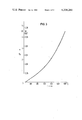
- FIG. 3 is a graphical illustration showing the dependence of heating capacity, P H , in watts for an exemplary 4 mm ⁇ 4 mm sensor element constructed in accordance with the principles of the invention, relative to an operative temperature range in ° C.
- a semiconductor body preferably composed of monocrystalline silicon and having a thickness of about 0.38 to 1 mm, is provided with an insulating SiO 2 layer 2 on all sides thereof, except side 1a, i.e., the underside in the illustrated arrangement.
- the insulating layer 2 has a thickness of at least equal to about 0.1 and not greater than about 1.0 ⁇ m.
- a highly doped n + shell zone 3 is generated on the outer surface of side 1a, for example by diffusing dopant elements therein or by ion implantation, for example with a trivalent or pentavalent element, such as phosphorous.
- the doped shell zone 3 functions as a heating layer.
- zone 3 is provided with spaced-apart contact metal strips 5, preferably comprised of vapor-deposited platinum.
- the metal oxide semiconductor layer 6 functions, at elevated temperatures, as a sensor for a select gas in air, for example, the exemplary SnO 2 layer functions as a sensor for ethyl alcohol vapors in air.
- Such metal oxide semiconductor layer is preferably about 50 nm thick and can be composed of select metal oxide semiconductors, such as the earlier mentioned tin oxide or platinum oxide or palladium oxide (sensors for carbon monoxide or hydrocarbons, respectively) or tin oxide having additions of niobium, vanadium, titanium and molybdenum (sensors for propane).
- select metal oxide semiconductors such as the earlier mentioned tin oxide or platinum oxide or palladium oxide (sensors for carbon monoxide or hydrocarbons, respectively) or tin oxide having additions of niobium, vanadium, titanium and molybdenum (sensors for propane).
- Two spaced-apart metal contact strips 7 and 8 are vaporized on the sensor layer 6 as shown.
- Connection wires 9 and 10 are joined to the heating layer 3 via contact strips 4 and 5 and connection wires 11 and 12 are joined to the sensor layer 6 via contact strips 7 and 8.
- connection wires 9 and 10 feed a current from a suitable source (not shown) to layer 3 for heating the same and wires 11 and 12 are connected to a resistance sensor (not shown) for determining any changes in electrical resistance in layer 6 upon the presence of a given gas in air.
- the connection wires 9, 10, 11 and 12 have a diameter of about 25 to 100 ⁇ m and can be composed of a metal selected from the group consisting of platinum, gold, aluminum and nickel.
- a semiconductor substrate 13 having approximately the same dimensions as described for body 1 in FIG. 1, is provided with an insulating SiO 2 layer 14 on all surfaces thereof except surface 13a.
- a highly doped p + shell zone 15 is generated on surface 13a by, for example, diffusing in boron atoms.
- a second SiO 2 layer 18 is generated on top of zone 15 via thermal oxidation. As shown, layer 18 terminates prior to the respective outer end regions of zone 15 and spaced-apart metal contact strips 16 and 17 are deposited on such outer end regions.
- Metal contact strips 20 and 21 are then positioned at opposite ends of the sensor layer 19.
- the heating contacts 16 and 17 are coupled to wires 24 and 25 for feeding a current to doped zone 15 so as to heat the same and sensor contacts 20 and 21 are coupled to wires 22 and 23 for monitoring a resistance of layer 19. With this arrangement, the heating layer 15 is located in the same side of substrate 13 as the sensor layer 19.
- the heating capacity value, W/mm 2 , per sensor area is shown on the right-hand scale.
- the curve illustrated was generated with an arrangement identical in structure with that illustrated at FIG. 1. This measurement curve shows that heat transmission occurs on a relatively steep heat conduction path and thus provides a low energy consumption. For example, with about 0.125 W/mm 2 , an operating temperature of about 400° C. is attained.
- All steps for producing sensor elements in accordance with the principles of the invention can be carried out with conventional silicon technology, that is, no additional assemblies are necessary and the arrangement can be produced via miniature construction techniques. Besides this, the heat transition with this type of arrangement occurs on a relatively short heat conduction path so that low energy consumption results.
- the energy outlay for a sensor element as illustrated in FIGS. 1 and 2 at a temperature of about 400° C., is approximately 130 mW/mm (see FIG. 3). Accordingly, by following the principles of the invention, it is possible to produce gas sensors having an energy consumption of only approximately 100 mW.
Abstract
Description
Claims (9)
Applications Claiming Priority (2)
| Application Number | Priority Date | Filing Date | Title |
|---|---|---|---|
| DE3019387A DE3019387C2 (en) | 1980-05-21 | 1980-05-21 | Thin-film semiconductor gas sensor with a heating element integrated into the sensor structure |
| DE3019387 | 1980-05-21 |
Publications (1)
| Publication Number | Publication Date |
|---|---|
| US4338281A true US4338281A (en) | 1982-07-06 |
Family
ID=6102965
Family Applications (1)
| Application Number | Title | Priority Date | Filing Date |
|---|---|---|---|
| US06/254,855 Expired - Fee Related US4338281A (en) | 1980-05-21 | 1981-04-16 | Thin film semiconductor gas sensor having an integrated heating element |
Country Status (4)
| Country | Link |
|---|---|
| US (1) | US4338281A (en) |
| JP (1) | JPS5717849A (en) |
| DE (1) | DE3019387C2 (en) |
| FR (1) | FR2484646A1 (en) |
Cited By (44)
| Publication number | Priority date | Publication date | Assignee | Title |
|---|---|---|---|---|
| US4387165A (en) * | 1982-04-22 | 1983-06-07 | Youngblood James L | H2 S Detector having semiconductor and noncontinuous inert film deposited thereon |
| US4442420A (en) * | 1982-09-30 | 1984-04-10 | Ford Motor Company | Partial pressure of oxygen sensor-II |
| US4443781A (en) * | 1981-04-27 | 1984-04-17 | Nippon Soken, Inc. | Gas detecting sensor |
| US4450428A (en) * | 1981-05-25 | 1984-05-22 | Nippon Soken, Inc. | Gas detecting sensor |
| US4453151A (en) * | 1982-06-07 | 1984-06-05 | Leary David J | Semiconductor gas sensor |
| US4457161A (en) * | 1980-10-09 | 1984-07-03 | Hitachi, Ltd. | Gas detection device and method for detecting gas |
| US4505803A (en) * | 1981-06-04 | 1985-03-19 | Ngk Insulators, Ltd. | Oxygen concentration detector |
| US4507643A (en) * | 1982-08-06 | 1985-03-26 | Naomasa Sunano | Gas sensor with improved perovskite type material |
| US4541988A (en) * | 1983-12-13 | 1985-09-17 | Bacharach Instrument Company | Constant temperature catalytic gas detection instrument |
| US4587105A (en) * | 1984-05-17 | 1986-05-06 | Honeywell Inc. | Integratable oxygen sensor |
| US4601914A (en) * | 1982-06-07 | 1986-07-22 | Airtech, Inc. | Method for fabricating a semiconductor gas sensor |
| US4688014A (en) * | 1983-04-11 | 1987-08-18 | New Cosmos Electric Co., Ltd. | Semiconductor type gas sensor having two terminals |
| US4916935A (en) * | 1983-11-09 | 1990-04-17 | Bacharach, Inc. | Low power solid state gas sensor with linear output and method of making the same |
| US4938928A (en) * | 1986-10-28 | 1990-07-03 | Figaro Engineering Inc. | Gas sensor |
| US4953387A (en) * | 1989-07-31 | 1990-09-04 | The Regents Of The University Of Michigan | Ultrathin-film gas detector |
| US4991424A (en) * | 1988-06-08 | 1991-02-12 | Vaisala Oy | Integrated heatable sensor |
| US5018518A (en) * | 1988-05-27 | 1991-05-28 | Gesellschaft Fur Geratebau Mbh | Gas work with sensing and alarm means |
| US5128514A (en) * | 1987-07-31 | 1992-07-07 | Siemens Aktiengesellschaft | Black radiator for use as an emitter in calibratable gas sensors |
| US5211053A (en) * | 1991-02-19 | 1993-05-18 | Robert Bosch Gmbh | Hot gas sensor device with improved thermal isolation from carrier plate |
| US5217692A (en) * | 1989-10-17 | 1993-06-08 | E.T.R. Elektronik Technologie Rump Gmbh | Gas sensor arrangement |
| US5382341A (en) * | 1992-09-10 | 1995-01-17 | Aroutiounian; Vladimir M. | Method of making smoke detector |
| US5500569A (en) * | 1993-04-07 | 1996-03-19 | Instrumentarium Oy | Electrically modulatable thermal radiant source and method for manufacturing the same |
| WO1996019724A1 (en) * | 1994-12-22 | 1996-06-27 | Senova Corporation | Apparatus for detecting selected chemical components of fluid streams |
| US5536473A (en) * | 1993-01-13 | 1996-07-16 | British Gas Plc | Polyaniline gas sensor |
| US5719325A (en) * | 1995-12-16 | 1998-02-17 | Dragerwerk Aktiengesellschaft | Gas sensor |
| US5830412A (en) * | 1993-09-30 | 1998-11-03 | Nittan Company Limited | Sensor device, and disaster prevention system and electronic equipment each having sensor device incorporated therein |
| US5891395A (en) * | 1993-03-15 | 1999-04-06 | Arizona Board Of Regents, A Body Corporate Of The State Of Arizona, Acting For And On Behalf Of Arizona State University | Chemical switch for detection of chemical components |
| US5985673A (en) * | 1994-12-22 | 1999-11-16 | Arizona Baord Of Regents | Method for regeneration of a sensor |
| US5994144A (en) * | 1992-03-04 | 1999-11-30 | Fujitsu Limited | Simplified environmental atmosphere measuring method |
| WO2000054841A1 (en) * | 1999-03-17 | 2000-09-21 | T.E.M.! Technische Entwicklungen Und Management Gmbh | Sensor device and method of detecting gases or fumes in air |
| US6596236B2 (en) | 1999-01-15 | 2003-07-22 | Advanced Technology Materials, Inc. | Micro-machined thin film sensor arrays for the detection of H2 containing gases, and method of making and using the same |
| US20040163445A1 (en) * | 2002-10-17 | 2004-08-26 | Dimeo Frank | Apparatus and process for sensing fluoro species in semiconductor processing systems |
| US20040211667A1 (en) * | 2003-04-24 | 2004-10-28 | Sacmi Cooperativa Meccanici Imola Soc. Coop. Ar.L. | Thin semiconductor film gas sensor device |
| US20060211253A1 (en) * | 2005-03-16 | 2006-09-21 | Ing-Shin Chen | Method and apparatus for monitoring plasma conditions in an etching plasma processing facility |
| US20090159446A1 (en) * | 2007-12-20 | 2009-06-25 | General Electric Company | Gas sensor and method of making |
| US20090305427A1 (en) * | 2002-10-17 | 2009-12-10 | Advanced Technology Materials, Inc. | Apparatus and process for sensing fluoro species in semiconductor processing systems |
| US20160341419A1 (en) * | 2015-05-18 | 2016-11-24 | E.G.O. Elektro-Geraetebau Gmbh | Heating device for heating fluids, and method for operating a heating device of this kind |
| EP3220142A1 (en) | 2016-03-18 | 2017-09-20 | Dräger Safety AG & Co. KGaA | Method for checking a gas sensor and gas measuring device, and gas warning system with a test device for checking a gas sensor |
| US10132769B2 (en) | 2016-07-13 | 2018-11-20 | Vaon, Llc | Doped, metal oxide-based chemical sensors |
| US10132786B2 (en) | 2016-03-18 | 2018-11-20 | Dräger Safety AG & Co. KGaA | Method for testing a gas sensor and gas-measuring device with a testing device for testing a gas sensor |
| US10802008B2 (en) | 2017-02-28 | 2020-10-13 | Vaon, Llc | Bimetal doped-metal oxide-based chemical sensors |
| US11203183B2 (en) | 2016-09-27 | 2021-12-21 | Vaon, Llc | Single and multi-layer, flat glass-sensor structures |
| US11275051B2 (en) | 2016-03-23 | 2022-03-15 | Vaon, Llc | Metal oxide-based chemical sensors |
| US11467138B2 (en) | 2016-09-27 | 2022-10-11 | Vaon, Llc | Breathalyzer |
Families Citing this family (7)
| Publication number | Priority date | Publication date | Assignee | Title |
|---|---|---|---|---|
| DE3217883A1 (en) * | 1982-05-12 | 1983-11-17 | Siemens AG, 1000 Berlin und 8000 München | Gas sensor |
| JPS59143945A (en) * | 1983-02-07 | 1984-08-17 | Richo Seiki Kk | Gas detecting device |
| JP2542643B2 (en) * | 1987-10-31 | 1996-10-09 | 株式会社東芝 | Sensor manufacturing method |
| JP2679811B2 (en) * | 1988-07-06 | 1997-11-19 | 株式会社リコー | Gas detector |
| JPH01284747A (en) * | 1988-05-10 | 1989-11-16 | Ricoh Co Ltd | Gas sensor |
| DE19606272C2 (en) * | 1996-02-21 | 2001-05-17 | Ust Umweltsensortechnik Gmbh | Semiconductor gas sensor |
| EP3715842B1 (en) * | 2019-03-26 | 2021-05-19 | Infineon Technologies AG | Mems gas sensor |
Citations (4)
| Publication number | Priority date | Publication date | Assignee | Title |
|---|---|---|---|---|
| US3751968A (en) * | 1971-01-22 | 1973-08-14 | Inficon Inc | Solid state sensor |
| US3865550A (en) * | 1970-08-26 | 1975-02-11 | Nat Res Dev | Semi-conducting gas sensitive devices |
| US3901067A (en) * | 1973-06-21 | 1975-08-26 | Gen Monitors | Semiconductor gas detector and method therefor |
| US4045178A (en) * | 1975-11-08 | 1977-08-30 | Matsushita Electric Industrial Co., Ltd. | Reducing gas sensor |
Family Cites Families (6)
| Publication number | Priority date | Publication date | Assignee | Title |
|---|---|---|---|---|
| FR2331016A1 (en) * | 1975-11-08 | 1977-06-03 | Matsushita Electric Ind Co Ltd | REDUCING GAS DETECTORS CONTAINING GAMMA FERRIC OXIDE AND AT LEAST ONE OTHER METAL OXIDE |
| GB1557921A (en) * | 1977-01-10 | 1979-12-19 | British Steel Corp | Gas monitors |
| US4224280A (en) * | 1977-07-18 | 1980-09-23 | Fuji Electric Co., Ltd. | Carbon monoxide detecting device |
| JPS5421397A (en) * | 1977-07-18 | 1979-02-17 | Fuji Electric Co Ltd | Carbon monoxide detector |
| DE2737385A1 (en) * | 1977-08-19 | 1979-03-22 | Licentia Gmbh | GAS DETECTING ELEMENT FOR DETECTING FATS AND ODOR SUBSTANCES |
| JPS5473097A (en) * | 1977-11-22 | 1979-06-12 | Seiko Epson Corp | Gas sensor |
-
1980
- 1980-05-21 DE DE3019387A patent/DE3019387C2/en not_active Expired
-
1981
- 1981-04-16 US US06/254,855 patent/US4338281A/en not_active Expired - Fee Related
- 1981-04-28 FR FR8108444A patent/FR2484646A1/en active Granted
- 1981-05-19 JP JP7560881A patent/JPS5717849A/en active Pending
Patent Citations (4)
| Publication number | Priority date | Publication date | Assignee | Title |
|---|---|---|---|---|
| US3865550A (en) * | 1970-08-26 | 1975-02-11 | Nat Res Dev | Semi-conducting gas sensitive devices |
| US3751968A (en) * | 1971-01-22 | 1973-08-14 | Inficon Inc | Solid state sensor |
| US3901067A (en) * | 1973-06-21 | 1975-08-26 | Gen Monitors | Semiconductor gas detector and method therefor |
| US4045178A (en) * | 1975-11-08 | 1977-08-30 | Matsushita Electric Industrial Co., Ltd. | Reducing gas sensor |
Cited By (60)
| Publication number | Priority date | Publication date | Assignee | Title |
|---|---|---|---|---|
| US4457161A (en) * | 1980-10-09 | 1984-07-03 | Hitachi, Ltd. | Gas detection device and method for detecting gas |
| US4443781A (en) * | 1981-04-27 | 1984-04-17 | Nippon Soken, Inc. | Gas detecting sensor |
| US4450428A (en) * | 1981-05-25 | 1984-05-22 | Nippon Soken, Inc. | Gas detecting sensor |
| US4505803A (en) * | 1981-06-04 | 1985-03-19 | Ngk Insulators, Ltd. | Oxygen concentration detector |
| US4387165A (en) * | 1982-04-22 | 1983-06-07 | Youngblood James L | H2 S Detector having semiconductor and noncontinuous inert film deposited thereon |
| US4453151A (en) * | 1982-06-07 | 1984-06-05 | Leary David J | Semiconductor gas sensor |
| US4601914A (en) * | 1982-06-07 | 1986-07-22 | Airtech, Inc. | Method for fabricating a semiconductor gas sensor |
| US4507643A (en) * | 1982-08-06 | 1985-03-26 | Naomasa Sunano | Gas sensor with improved perovskite type material |
| US4442420A (en) * | 1982-09-30 | 1984-04-10 | Ford Motor Company | Partial pressure of oxygen sensor-II |
| US4688014A (en) * | 1983-04-11 | 1987-08-18 | New Cosmos Electric Co., Ltd. | Semiconductor type gas sensor having two terminals |
| US4916935A (en) * | 1983-11-09 | 1990-04-17 | Bacharach, Inc. | Low power solid state gas sensor with linear output and method of making the same |
| US4541988A (en) * | 1983-12-13 | 1985-09-17 | Bacharach Instrument Company | Constant temperature catalytic gas detection instrument |
| US4587105A (en) * | 1984-05-17 | 1986-05-06 | Honeywell Inc. | Integratable oxygen sensor |
| US4938928A (en) * | 1986-10-28 | 1990-07-03 | Figaro Engineering Inc. | Gas sensor |
| US5128514A (en) * | 1987-07-31 | 1992-07-07 | Siemens Aktiengesellschaft | Black radiator for use as an emitter in calibratable gas sensors |
| US5018518A (en) * | 1988-05-27 | 1991-05-28 | Gesellschaft Fur Geratebau Mbh | Gas work with sensing and alarm means |
| US4991424A (en) * | 1988-06-08 | 1991-02-12 | Vaisala Oy | Integrated heatable sensor |
| US4953387A (en) * | 1989-07-31 | 1990-09-04 | The Regents Of The University Of Michigan | Ultrathin-film gas detector |
| US5217692A (en) * | 1989-10-17 | 1993-06-08 | E.T.R. Elektronik Technologie Rump Gmbh | Gas sensor arrangement |
| US5211053A (en) * | 1991-02-19 | 1993-05-18 | Robert Bosch Gmbh | Hot gas sensor device with improved thermal isolation from carrier plate |
| US5994144A (en) * | 1992-03-04 | 1999-11-30 | Fujitsu Limited | Simplified environmental atmosphere measuring method |
| US5382341A (en) * | 1992-09-10 | 1995-01-17 | Aroutiounian; Vladimir M. | Method of making smoke detector |
| US5536473A (en) * | 1993-01-13 | 1996-07-16 | British Gas Plc | Polyaniline gas sensor |
| US5939020A (en) * | 1993-03-15 | 1999-08-17 | The Arizona Board Of Regents, A Body Corporate Of The State Of Arizona, Acting For And On Behalf Of Arizona State University | Chemical switch for detection of chemical components |
| US5891395A (en) * | 1993-03-15 | 1999-04-06 | Arizona Board Of Regents, A Body Corporate Of The State Of Arizona, Acting For And On Behalf Of Arizona State University | Chemical switch for detection of chemical components |
| US5500569A (en) * | 1993-04-07 | 1996-03-19 | Instrumentarium Oy | Electrically modulatable thermal radiant source and method for manufacturing the same |
| US5830412A (en) * | 1993-09-30 | 1998-11-03 | Nittan Company Limited | Sensor device, and disaster prevention system and electronic equipment each having sensor device incorporated therein |
| US5985673A (en) * | 1994-12-22 | 1999-11-16 | Arizona Baord Of Regents | Method for regeneration of a sensor |
| WO1996019724A1 (en) * | 1994-12-22 | 1996-06-27 | Senova Corporation | Apparatus for detecting selected chemical components of fluid streams |
| US5719325A (en) * | 1995-12-16 | 1998-02-17 | Dragerwerk Aktiengesellschaft | Gas sensor |
| US6596236B2 (en) | 1999-01-15 | 2003-07-22 | Advanced Technology Materials, Inc. | Micro-machined thin film sensor arrays for the detection of H2 containing gases, and method of making and using the same |
| US20030153088A1 (en) * | 1999-01-15 | 2003-08-14 | Dimeo Frank | Micro-machined thin film sensor arrays for the detection of H2, NH3, and sulfur containing gases, and method of making and using the same |
| WO2000054841A1 (en) * | 1999-03-17 | 2000-09-21 | T.E.M.! Technische Entwicklungen Und Management Gmbh | Sensor device and method of detecting gases or fumes in air |
| WO2000054840A1 (en) * | 1999-03-17 | 2000-09-21 | T.E.M.! Technische Entwicklungen Und Management Gmbh | Method and sensor device for detecting gases or fumes in air |
| US20040163445A1 (en) * | 2002-10-17 | 2004-08-26 | Dimeo Frank | Apparatus and process for sensing fluoro species in semiconductor processing systems |
| US20090305427A1 (en) * | 2002-10-17 | 2009-12-10 | Advanced Technology Materials, Inc. | Apparatus and process for sensing fluoro species in semiconductor processing systems |
| US8109130B2 (en) | 2002-10-17 | 2012-02-07 | Advanced Technology Materials, Inc. | Apparatus and process for sensing fluoro species in semiconductor processing systems |
| US20040211667A1 (en) * | 2003-04-24 | 2004-10-28 | Sacmi Cooperativa Meccanici Imola Soc. Coop. Ar.L. | Thin semiconductor film gas sensor device |
| WO2004095013A1 (en) * | 2003-04-24 | 2004-11-04 | Sacmi Cooperativa Meccanici Imola Societa' Cooperativa | A thin semiconductor film gas sensor device |
| US7441440B2 (en) | 2003-04-24 | 2008-10-28 | Sacmi Cooperativa Meccanici Imola Soc. Coop. A.R.L. | Thin semiconductor film gas sensor device |
| US20060211253A1 (en) * | 2005-03-16 | 2006-09-21 | Ing-Shin Chen | Method and apparatus for monitoring plasma conditions in an etching plasma processing facility |
| US20080134757A1 (en) * | 2005-03-16 | 2008-06-12 | Advanced Technology Materials, Inc. | Method And Apparatus For Monitoring Plasma Conditions In An Etching Plasma Processing Facility |
| US20090159446A1 (en) * | 2007-12-20 | 2009-06-25 | General Electric Company | Gas sensor and method of making |
| US7827852B2 (en) * | 2007-12-20 | 2010-11-09 | General Electric Company | Gas sensor and method of making |
| CN106196560A (en) * | 2015-05-18 | 2016-12-07 | E.G.O.电气设备制造股份有限公司 | The heater adding hot fluid and the method operating this heater |
| US20160341419A1 (en) * | 2015-05-18 | 2016-11-24 | E.G.O. Elektro-Geraetebau Gmbh | Heating device for heating fluids, and method for operating a heating device of this kind |
| RU2717955C2 (en) * | 2015-05-18 | 2020-03-27 | Э.Г.О. Электро-Геретебау Гмбх | Heating device for heating fluids and a method of controlling such a device |
| CN106196560B (en) * | 2015-05-18 | 2022-07-05 | E.G.O.电气设备制造股份有限公司 | Heating device for heating a fluid and method for operating such a heating device |
| EP3220142A1 (en) | 2016-03-18 | 2017-09-20 | Dräger Safety AG & Co. KGaA | Method for checking a gas sensor and gas measuring device, and gas warning system with a test device for checking a gas sensor |
| DE102016003284A1 (en) | 2016-03-18 | 2017-09-21 | Dräger Safety AG & Co. KGaA | Method for checking a gas sensor and gas measuring device with a test device for checking a gas sensor |
| US10132786B2 (en) | 2016-03-18 | 2018-11-20 | Dräger Safety AG & Co. KGaA | Method for testing a gas sensor and gas-measuring device with a testing device for testing a gas sensor |
| DE102016003283B4 (en) | 2016-03-18 | 2022-05-19 | Dräger Safety AG & Co. KGaA | Gas measuring device with a test device for checking a gas sensor |
| DE102016003284B4 (en) | 2016-03-18 | 2022-05-19 | Dräger Safety AG & Co. KGaA | Gas measuring device with a test device for checking a gas sensor |
| US11209385B2 (en) | 2016-03-18 | 2021-12-28 | Dräger Safety AG & Co. KGaA | Method for testing a gas sensor and gas-measuring device with a testing device for testing a gas sensor |
| US11275051B2 (en) | 2016-03-23 | 2022-03-15 | Vaon, Llc | Metal oxide-based chemical sensors |
| US10132769B2 (en) | 2016-07-13 | 2018-11-20 | Vaon, Llc | Doped, metal oxide-based chemical sensors |
| US11009475B2 (en) | 2016-07-13 | 2021-05-18 | Vaon, Llc | Doped, metal oxide-based chemical sensors |
| US11203183B2 (en) | 2016-09-27 | 2021-12-21 | Vaon, Llc | Single and multi-layer, flat glass-sensor structures |
| US11467138B2 (en) | 2016-09-27 | 2022-10-11 | Vaon, Llc | Breathalyzer |
| US10802008B2 (en) | 2017-02-28 | 2020-10-13 | Vaon, Llc | Bimetal doped-metal oxide-based chemical sensors |
Also Published As
| Publication number | Publication date |
|---|---|
| DE3019387A1 (en) | 1981-11-26 |
| DE3019387C2 (en) | 1986-01-23 |
| FR2484646A1 (en) | 1981-12-18 |
| JPS5717849A (en) | 1982-01-29 |
| FR2484646B1 (en) | 1985-02-08 |
Similar Documents
| Publication | Publication Date | Title |
|---|---|---|
| US4338281A (en) | Thin film semiconductor gas sensor having an integrated heating element | |
| US4500412A (en) | Oxygen sensor with heater | |
| US5500569A (en) | Electrically modulatable thermal radiant source and method for manufacturing the same | |
| EP0776023B1 (en) | Electrically modulatable thermal radiant source | |
| US4343768A (en) | Gas detector | |
| CN100538920C (en) | Stable pyrostat/heater system with tungsten/aluminium nitride | |
| US3695848A (en) | Gas detecting device | |
| Gardner et al. | Integrated tin oxide odour sensors | |
| US4505783A (en) | Oxygen concentration detector and method of using same | |
| US4703555A (en) | Method of making a catalytic-burning sensor | |
| EP0689229A2 (en) | Electrically modulatable thermal radiant source | |
| US5012671A (en) | Gas detecting device | |
| US4016524A (en) | Sensor for a gas detector, in particular for smoke detection | |
| US5382341A (en) | Method of making smoke detector | |
| JPH053895B2 (en) | ||
| US5685969A (en) | Sensor arrangement | |
| US4198850A (en) | Gas sensors | |
| EP0334614A3 (en) | Catalytic gas detector | |
| CA1276230C (en) | Oxygen sensor | |
| JPH053894B2 (en) | ||
| JPH0862168A (en) | Nitrogen oxide detecting device | |
| JP2955583B2 (en) | Detection element for gas sensor | |
| KR102503494B1 (en) | Hydrogen detection sensor | |
| JP3845937B2 (en) | Gas sensor | |
| JPH0220681Y2 (en) |
Legal Events
| Date | Code | Title | Description |
|---|---|---|---|
| AS | Assignment |
Owner name: SIEMENS AKTIENGESELLSCHAFT, BERLIN AND MUNICH A CO Free format text: ASSIGNMENT OF ASSIGNORS INTEREST.;ASSIGNORS:TREITINGER LUDWIG;TISCHER PETER;SCHNEIDER-GMELCH BRIGITTE;REEL/FRAME:003879/0647 Effective date: 19810327 |
|
| MAFP | Maintenance fee payment |
Free format text: PAYMENT OF MAINTENANCE FEE, 4TH YEAR, PL 96-517 (ORIGINAL EVENT CODE: M170); ENTITY STATUS OF PATENT OWNER: LARGE ENTITY Year of fee payment: 4 |
|
| FEPP | Fee payment procedure |
Free format text: PAYOR NUMBER ASSIGNED (ORIGINAL EVENT CODE: ASPN); ENTITY STATUS OF PATENT OWNER: LARGE ENTITY |
|
| FEPP | Fee payment procedure |
Free format text: MAINTENANCE FEE REMINDER MAILED (ORIGINAL EVENT CODE: REM.); ENTITY STATUS OF PATENT OWNER: LARGE ENTITY |
|
| LAPS | Lapse for failure to pay maintenance fees | ||
| STCH | Information on status: patent discontinuation |
Free format text: PATENT EXPIRED DUE TO NONPAYMENT OF MAINTENANCE FEES UNDER 37 CFR 1.362 |
|
| FP | Lapsed due to failure to pay maintenance fee |
Effective date: 19900708 |