US4365242A - Driving technique for matrix liquid crystal display panel for displaying characters and a cursor - Google Patents
Driving technique for matrix liquid crystal display panel for displaying characters and a cursor Download PDFInfo
- Publication number
- US4365242A US4365242A US06/237,702 US23770281A US4365242A US 4365242 A US4365242 A US 4365242A US 23770281 A US23770281 A US 23770281A US 4365242 A US4365242 A US 4365242A
- Authority
- US
- United States
- Prior art keywords
- scanning
- cursor
- line
- rows
- liquid crystal
- Prior art date
- Legal status (The legal status is an assumption and is not a legal conclusion. Google has not performed a legal analysis and makes no representation as to the accuracy of the status listed.)
- Expired - Lifetime
Links
Images


Classifications
-
- G—PHYSICS
- G09—EDUCATION; CRYPTOGRAPHY; DISPLAY; ADVERTISING; SEALS
- G09G—ARRANGEMENTS OR CIRCUITS FOR CONTROL OF INDICATING DEVICES USING STATIC MEANS TO PRESENT VARIABLE INFORMATION
- G09G3/00—Control arrangements or circuits, of interest only in connection with visual indicators other than cathode-ray tubes
- G09G3/20—Control arrangements or circuits, of interest only in connection with visual indicators other than cathode-ray tubes for presentation of an assembly of a number of characters, e.g. a page, by composing the assembly by combination of individual elements arranged in a matrix no fixed position being assigned to or needed to be assigned to the individual characters or partial characters
- G09G3/34—Control arrangements or circuits, of interest only in connection with visual indicators other than cathode-ray tubes for presentation of an assembly of a number of characters, e.g. a page, by composing the assembly by combination of individual elements arranged in a matrix no fixed position being assigned to or needed to be assigned to the individual characters or partial characters by control of light from an independent source
- G09G3/36—Control arrangements or circuits, of interest only in connection with visual indicators other than cathode-ray tubes for presentation of an assembly of a number of characters, e.g. a page, by composing the assembly by combination of individual elements arranged in a matrix no fixed position being assigned to or needed to be assigned to the individual characters or partial characters by control of light from an independent source using liquid crystals
-
- G—PHYSICS
- G09—EDUCATION; CRYPTOGRAPHY; DISPLAY; ADVERTISING; SEALS
- G09G—ARRANGEMENTS OR CIRCUITS FOR CONTROL OF INDICATING DEVICES USING STATIC MEANS TO PRESENT VARIABLE INFORMATION
- G09G3/00—Control arrangements or circuits, of interest only in connection with visual indicators other than cathode-ray tubes
- G09G3/04—Control arrangements or circuits, of interest only in connection with visual indicators other than cathode-ray tubes for presentation of a single character by selection from a plurality of characters, or by composing the character by combination of individual elements, e.g. segments using a combination of such display devices for composing words, rows or the like, in a frame with fixed character positions
- G09G3/16—Control arrangements or circuits, of interest only in connection with visual indicators other than cathode-ray tubes for presentation of a single character by selection from a plurality of characters, or by composing the character by combination of individual elements, e.g. segments using a combination of such display devices for composing words, rows or the like, in a frame with fixed character positions by control of light from an independent source
- G09G3/18—Control arrangements or circuits, of interest only in connection with visual indicators other than cathode-ray tubes for presentation of a single character by selection from a plurality of characters, or by composing the character by combination of individual elements, e.g. segments using a combination of such display devices for composing words, rows or the like, in a frame with fixed character positions by control of light from an independent source using liquid crystals
-
- G—PHYSICS
- G09—EDUCATION; CRYPTOGRAPHY; DISPLAY; ADVERTISING; SEALS
- G09G—ARRANGEMENTS OR CIRCUITS FOR CONTROL OF INDICATING DEVICES USING STATIC MEANS TO PRESENT VARIABLE INFORMATION
- G09G5/00—Control arrangements or circuits for visual indicators common to cathode-ray tube indicators and other visual indicators
- G09G5/08—Cursor circuits
Definitions
- This invention relates to a driving technique for a liquid crystal matrix display panel wherein the brightness is dependent on the effective value of an applied voltage.
- matrix display panels having signal lines and scanning lines in a matrix and a plurality of pixels at the crossings of these lines typically twisted nematic liquid crystal matrix panels possess the dependency of its brightness of respective ones of the pixels on the effective value of applied voltages thereto.
- an electrode structure per character (character, number, symbol or the like) is set up by five data column electrodes 1, seven scanning row electrodes 2 and a single cursor line electrode 3 as depicted in FIG. 1.
- the respective scanning row electrodes 2 and the cursor line electrode 3 are conventionally scanned in a line sequential fashion for displaying characters.
- V rms (ON) is the effective value of an ON voltage applied across a respective one of the liquid crystal pixels
- V rms (OFF) is the effective value of an OFF voltage applied thereto
- N is the number of the scanning lines.
- FIG. 1 is a view of an electrode scheme of a liquid crystal matrix display panel
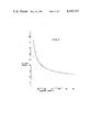
- FIG. 2 is a graph showing the relationship between the number of scanning lines and voltage margin
- FIG. 3 is a block diagram of an embodiment of the present invention.
- FIG. 4 is a block diagram of a cursor line control circuit
- FIG. 5 is a circuit diagram of a cursor selector
- FIG. 6 is a view for explanation of cursor line driving.
- a driving circuit for a 20 characters by 8 rows liquid crystal display panel for displaying characters which includes a keyboard 4, an input/output interface 5, a character buffer memory 6, a character generator 7, a parallel-to-serial converter 8, a frame memory 9, a memory control circuit 10, line memories 11a, 11b, 11c and 11d, data latches 12a, 12b, 12c and 12d, drivers 13a, 13b, 13c and 13d, the liquid crystal panel 14, an oscillator 15, a timing control circuit 16, a scanning circuit 17 and a cursor line selector 18.
- the output of the keyboard 4 as an input device is supplied to the character buffer memory 6 via the imput/output interface 5.
- the character buffer memory 6 is a memory which temporarily stores the output of the keyboard 4 and provides its output for the character generator 7.
- the character generator 7 comprises a memory typically of a read only memory (ROM) for generating desired character signals corresponding to the outputs of the keyboard 4 in response to the signals from the character buffer memory 6.
- the parallel outputs of the character generator 7 are converted into serial signals via the parallel-to-serial converter 8 and loaded into the frame memory 9.
- the frame memory 9 has four random access memories (RAM) 9a, 9b, 9c and 9d each capable of storing 20 characters by 2 rows of the serial converted character signals under control of the memory control circuit 10.
- RAM random access memories
- the respective outputs of the random access memories are fed to the line memories 11a, 11b, 11c and 11d.
- the above-mentioned line memories 11a, 11b, 11c and 11d are buffer memories which temporarily store data signals transferred from the frame memories 9a, 9b, 9c and 9d to the column electrodes 1 of liquid crystal display panel units 14a, 14b, 14c and 14d per scanning line.
- the respective outputs of the line memories 11a, 11b, 11c and 11d are supplied via the data latches 12a, 12b, 12c and 12d to the driver circuits 13a, 13b, 13c and 13d which in turn drive the respective column electrodes 1 of the liquid crystal display panel units 14a, 14b, 14c and 14d in synchronism with scanning timing signals from the scanning circuit 12 discussed in detail later.
- the liquid crystal panel units 14a, 14b, 14c and 14d are each a liquid crystal display capable of displaying 20 characters by 2 rows with the same electrode configuration as shown in FIG. 1 and form as a whole the single panel 14 capable of 20 characters by 8 lines.
- the liquid crystal panel 14 is typically made up such that two rows of characters form a pair and the column electrodes 1 are subdivided into two groups in a vertical direction to thereby form a pair of the units 14a and 14b and a pair of the units 14c and 14d and each of the units are further double-layered.
- Corresponding ones of the row electrodes 2 of the liquid crystal display units 14a, 14b, 14c and 14d and corresponding ones of the cursor electrodes 3 are connected in common. These row electrodes 2 are scanned in the line sequential scanning fashion by the scanning circuit 17 and then one of the two cursors 3 is selected and driven. This selection is achieved in such a manner that the position where the cursor lines is to be displayed is detected by the cursor line control circuit in the timing circuit 16 as best shown in FIG. 4 and the output of the cursor line control circuit is supplied to the cursor selector 18 and the scanning circuit 17 selects one of the cursor electrodes 3 in response to the output of the cursor line selector 18.
- the timing control circuit 16 is a circuit which generates a variety of various timing signals in response to clock pulses from the oscillator 15 and one-character strobe signals from the input/output interface 5. Those timing pulses are fed to the input/output interface 5, the character buffer memory 6, the character generator 7, the parallel-to-serial converter 8, the memory control circuit 10, the line memories 11a, 11b, 11c and 11d, the data latches 12a, 12b, 12c and 12d and the scanning control circuit 17, while the cursor line control circuit in the timing control circuit 16 supplies a signal indicative of the position for displaying the cursor line to the cursor line selector 18.
- the cursor line control circuit includes a 5-bit 1-up horizontal line counter 19, a horizontal comparator 20, a horizontal up/down counter 21, a 7-line 1-up vertical line counter 22, a vertical comparator 23, a vertical up-down counter 24, a radix-of-15 counter 25, a cursor line position agreement detector 26, a cursor line counter 27, an AND gate 28, an OR gate 29, etc.
- a respective one of the pixels corresponds to 1 bit while viewing from the column electrodes 1 of the liquid crystal panel units 14a, 14b, 14c and 14d.
- the timing control circuit 16 of FIG. 3 supplies 5-bit signals to the 5-bit 1-up horizontal counter 19 for transferring each character in a horizontal direction every 5 bits (when each character consists of 5 by 7 dots).
- the 5-bit signals are introduced into the 5-bit 1-up horizontal counter 19 to count the number of the characters.
- the 1-character strobe signals fed via the keyboard 4 of FIG. 3 are sent to and counted by the horizontal up/down counter 21 for detecting the horizontal position of a character introduced via the keyboard 4.
- the horizontal comparator 20 compares the output of the horizontal line counter 19 and the counterpart of the horizontal up/down counter 21 and sense character position signals.
- 7-line signals each consisting of 7 line signals as a unit per 7 row electrodes 2 of the liquid crystal panel units 14a, 14b, 14c and 14d are transferred from the timing control circuit 5 to the 7-line 1-up vertical line counter 22 to count the number of rows.
- Carry signals developing per row of the characters are transferred from the horizontal up/down counter 21 to the vertical up/down counter 24 to count the number of rows.
- the vertical comparator 23 compares the output of the 7-line 1-up vertical line counter 22 and the output of the vertical up/down counter 24 to sense where the character is next written.
- the scanning signals generated per line or each of the row lines 2 from the timing control circuit 16 or 1-line signals are supplied to the radix-of-15 counter 25 which is incremented to generate 15-line signals per 15 lines or 15 row electrodes.
- the 15-line signals are then supplied to increment the cursor line counter 27 by one.
- the output of the cursor line counter 27 and part of the output of the vertical up/down counter 24 are led into the cursor line position agreement detector 26 which in turn provides a cursor signals if the both agree. Since the character position signals from the horizontal comparator 20 are also supplied to the cursor position detector 26 under these circumstances, the cursor signal indicates not only the row position but also the horizontal position of the cursor line. Having been gated via the AND gate 28 in response to the 15-line signals, the cursor signal is mixed with the character or numerical data signals via the OR gate 29 into a frame memory data signal.
- a cursor line selection signal from the output Q A of the vertical up/down counter 24 is a signal which alternates between "0" and "1" each line or row.
- the cursor line selection signal is supplied to the cursor line selector 18 which includes two AND gates 30 and 31 and an inverter 32 as shown in FIG. 5.
- the AND gate 31 is open to enable the upper of the cursor line electrodes 3 (odd cursor electrodes) of the liquid crystal display units 14a, 14b, 14c and 14d as shown in FIG. 6, while the cursor line selection signal of a "1" level enables the even cursor electrodes 3 of the liquid crystal panel 14.
- the above driving technique eliminates the need for a scanning line for the single cursor line electrode 3 per frame for each of the liquid crystal display units 14a, 14b, 14c and 14d with a reduction of a total of the number of the scanning lines.
- V 0 is the threshold level (peak value) of liquid crystal material on the column electrode side.
- the capacity of the frame memory 9 can be reduced from 6400 bits to 6000 bits but the voltage margin be increased from 1.29 to 1.30 according to the present invention.
- the present invention makes it possible to take a multiplexing degree of 19 rather than 20 in the case of a 7 by 9 dot matrix. It is also obvious that the concept of the present invention is equally applicable to display panels of other materials other than the above discussed liquid crystal material as long as they have separate column electrodes.
- the driving technique according to the present invention scans the scanning lines where no cursor line is displayed like the interlaced scanning manner in the art of television transmission. The result is a decrease in the number of the scanning lines and an increase in the voltage margin with high contrast and wide viewing angle properties.
Abstract
Description
TABLE 1 ______________________________________Multiplexing degree 16 15 Frame memory capacity 6400 bits 6000 bits Voltage margin 1.29 1.30 Optimum voltage (scanning side) ±4 V.sub.0 ±3.87 V.sub.0 ______________________________________
Claims (3)
Applications Claiming Priority (2)
| Application Number | Priority Date | Filing Date | Title |
|---|---|---|---|
| JP2300380A JPS56119192A (en) | 1980-02-25 | 1980-02-25 | Method of driving liquid crystal matric display unit |
| JP55-23003 | 1980-02-25 |
Publications (1)
| Publication Number | Publication Date |
|---|---|
| US4365242A true US4365242A (en) | 1982-12-21 |
Family
ID=12098318
Family Applications (1)
| Application Number | Title | Priority Date | Filing Date |
|---|---|---|---|
| US06/237,702 Expired - Lifetime US4365242A (en) | 1980-02-25 | 1981-02-24 | Driving technique for matrix liquid crystal display panel for displaying characters and a cursor |
Country Status (4)
| Country | Link |
|---|---|
| US (1) | US4365242A (en) |
| JP (1) | JPS56119192A (en) |
| DE (1) | DE3107026C2 (en) |
| GB (1) | GB2070836B (en) |
Cited By (10)
| Publication number | Priority date | Publication date | Assignee | Title |
|---|---|---|---|---|
| US4710766A (en) * | 1983-08-25 | 1987-12-01 | Societe Francaise D'equipements Pour La Navigation Aerienne | Device for displaying symbols by means of a liquid crystal matrix |
| US4751502A (en) * | 1985-03-27 | 1988-06-14 | Ascii Corporation | Display controller for displaying a cursor on either of a CRT display device or a liquid crystal display device |
| US4764763A (en) * | 1985-12-13 | 1988-08-16 | The Ohio Art Company | Electronic sketching device |
| US4825202A (en) * | 1985-09-16 | 1989-04-25 | Commissariat A L'energie Atomique | Control means for an integrated memory matrix display and its control process |
| US4887968A (en) * | 1985-12-13 | 1989-12-19 | The Ohio Art Company | Electronic sketching device |
| US5166670A (en) * | 1989-12-27 | 1992-11-24 | Sharp Kabushiki Kaisha | Column electrode driving circuit for a display apparatus |
| US5361081A (en) * | 1993-04-29 | 1994-11-01 | Digital Equipment Corporation | Programmable pixel and scan-line offsets for a hardware cursor |
| US5896114A (en) * | 1993-11-11 | 1999-04-20 | Seiko Epson Corporation | Matrix type display device, electronic system including the same and method of driving such a display device |
| US5933010A (en) * | 1998-01-13 | 1999-08-03 | Moreno; Gil G. | Device to detect charging condition of a storage battery |
| US20060097981A1 (en) * | 2004-11-10 | 2006-05-11 | Chul-Woo Park | Liquid crystal display and driving method thereof |
Families Citing this family (2)
| Publication number | Priority date | Publication date | Assignee | Title |
|---|---|---|---|---|
| JPS59121391A (en) * | 1982-12-28 | 1984-07-13 | シチズン時計株式会社 | Liquid crystal display |
| CH666563A5 (en) * | 1985-01-10 | 1988-07-29 | Landis & Gyr Ag | HEATING CONTROLLER WITH A PROGRAM SWITCH. |
Citations (4)
| Publication number | Priority date | Publication date | Assignee | Title |
|---|---|---|---|---|
| US3979718A (en) * | 1971-12-23 | 1976-09-07 | Fujitsu Ltd. | Method of driving a plasma display panel |
| US4281324A (en) * | 1977-10-31 | 1981-07-28 | Sharp Kabushiki Kaisha | Matrix type liquid crystal display |
| US4307391A (en) * | 1978-08-30 | 1981-12-22 | Pelikan Aktiengesellschaft | Desk information display device |
| US4308534A (en) * | 1978-12-08 | 1981-12-29 | Kabushiki Kaisha Daini Seikosha | Multiplexing liquid crystal display device having different display formats |
Family Cites Families (2)
| Publication number | Priority date | Publication date | Assignee | Title |
|---|---|---|---|---|
| JPS5330231A (en) * | 1976-09-01 | 1978-03-22 | Nec Corp | Cursor display system |
| JPS5458399A (en) * | 1977-10-18 | 1979-05-11 | Sharp Corp | Matrix type liquid crystal display unit |
-
1980
- 1980-02-25 JP JP2300380A patent/JPS56119192A/en active Pending
-
1981
- 1981-02-24 US US06/237,702 patent/US4365242A/en not_active Expired - Lifetime
- 1981-02-24 GB GB8105738A patent/GB2070836B/en not_active Expired
- 1981-02-25 DE DE3107026A patent/DE3107026C2/en not_active Expired
Patent Citations (4)
| Publication number | Priority date | Publication date | Assignee | Title |
|---|---|---|---|---|
| US3979718A (en) * | 1971-12-23 | 1976-09-07 | Fujitsu Ltd. | Method of driving a plasma display panel |
| US4281324A (en) * | 1977-10-31 | 1981-07-28 | Sharp Kabushiki Kaisha | Matrix type liquid crystal display |
| US4307391A (en) * | 1978-08-30 | 1981-12-22 | Pelikan Aktiengesellschaft | Desk information display device |
| US4308534A (en) * | 1978-12-08 | 1981-12-29 | Kabushiki Kaisha Daini Seikosha | Multiplexing liquid crystal display device having different display formats |
Cited By (11)
| Publication number | Priority date | Publication date | Assignee | Title |
|---|---|---|---|---|
| US4710766A (en) * | 1983-08-25 | 1987-12-01 | Societe Francaise D'equipements Pour La Navigation Aerienne | Device for displaying symbols by means of a liquid crystal matrix |
| US4751502A (en) * | 1985-03-27 | 1988-06-14 | Ascii Corporation | Display controller for displaying a cursor on either of a CRT display device or a liquid crystal display device |
| US4825202A (en) * | 1985-09-16 | 1989-04-25 | Commissariat A L'energie Atomique | Control means for an integrated memory matrix display and its control process |
| US4764763A (en) * | 1985-12-13 | 1988-08-16 | The Ohio Art Company | Electronic sketching device |
| US4887968A (en) * | 1985-12-13 | 1989-12-19 | The Ohio Art Company | Electronic sketching device |
| US5166670A (en) * | 1989-12-27 | 1992-11-24 | Sharp Kabushiki Kaisha | Column electrode driving circuit for a display apparatus |
| US5361081A (en) * | 1993-04-29 | 1994-11-01 | Digital Equipment Corporation | Programmable pixel and scan-line offsets for a hardware cursor |
| US5896114A (en) * | 1993-11-11 | 1999-04-20 | Seiko Epson Corporation | Matrix type display device, electronic system including the same and method of driving such a display device |
| US5933010A (en) * | 1998-01-13 | 1999-08-03 | Moreno; Gil G. | Device to detect charging condition of a storage battery |
| US20060097981A1 (en) * | 2004-11-10 | 2006-05-11 | Chul-Woo Park | Liquid crystal display and driving method thereof |
| CN100426060C (en) * | 2004-11-10 | 2008-10-15 | 三星Sdi株式会社 | Liquid crystal display and driving method thereof |
Also Published As
| Publication number | Publication date |
|---|---|
| DE3107026A1 (en) | 1982-01-07 |
| GB2070836A (en) | 1981-09-09 |
| GB2070836B (en) | 1984-01-25 |
| DE3107026C2 (en) | 1985-02-21 |
| JPS56119192A (en) | 1981-09-18 |
Similar Documents
| Publication | Publication Date | Title |
|---|---|---|
| US5196839A (en) | Gray scales method and circuitry for flat panel graphics display | |
| US5172108A (en) | Multilevel image display method and system | |
| US5764212A (en) | Matrix type liquid crystal display device with data electrode driving circuit in which display information for one screen is written into and read out from display memory at mutually different frequencies | |
| EP0193728A2 (en) | Display control system | |
| US4365242A (en) | Driving technique for matrix liquid crystal display panel for displaying characters and a cursor | |
| EP0154067A1 (en) | Display apparatus with mixed alphanumeric and graphic image | |
| US6320562B1 (en) | Liquid crystal display device | |
| JPH10133172A (en) | Simple matrix display device drive circuit | |
| US5252959A (en) | Method and apparatus for controlling a multigradation display | |
| JP2804059B2 (en) | Liquid crystal display | |
| US5379051A (en) | Method and apparatus for rearranging and displaying line data | |
| US6559823B1 (en) | Method of driving STN liquid crystal panel and apparatus therefor | |
| US5754157A (en) | Method for forming column signals for a liquid crystal display apparatus | |
| US4345244A (en) | Video output circuit for high resolution character generator in a digital display unit | |
| US6597335B2 (en) | Liquid crystal display device and method for driving the same | |
| CA1107870A (en) | Rise and fall line insertion circuitry | |
| US5745089A (en) | Method for driving apparatus | |
| US20030063109A1 (en) | Flat-panel display device | |
| EP0123896A2 (en) | Character and video mode control circuit | |
| US5068651A (en) | Image display apparatus | |
| JP4564747B2 (en) | Multi-tone image display device using pulse width modulation drive system | |
| US5206630A (en) | Improved driving circuit for a gaseous discharge display device which provides reduced power consumption | |
| US6486865B1 (en) | Semiconductor device, image display system and electronic system | |
| US5107255A (en) | Control device for a display apparatus | |
| US6091387A (en) | Liquid crystal display device and driving method of the same |
Legal Events
| Date | Code | Title | Description |
|---|---|---|---|
| AS | Assignment |
Owner name: SHARP KABUSHIKI KAISHA, 22-22 NAGAIKE-CHO, ABENO-K Free format text: ASSIGNMENT OF ASSIGNORS INTEREST.;ASSIGNORS:YASUDA SHUHEI;ISHII YUTAKA;WADA TOMIO;REEL/FRAME:003870/0812 Effective date: 19810213 |
|
| STCF | Information on status: patent grant |
Free format text: PATENTED CASE |
|
| MAFP | Maintenance fee payment |
Free format text: PAYMENT OF MAINTENANCE FEE, 4TH YEAR, PL 96-517 (ORIGINAL EVENT CODE: M170); ENTITY STATUS OF PATENT OWNER: LARGE ENTITY Year of fee payment: 4 |
|
| FEPP | Fee payment procedure |
Free format text: PAYOR NUMBER ASSIGNED (ORIGINAL EVENT CODE: ASPN); ENTITY STATUS OF PATENT OWNER: LARGE ENTITY |
|
| MAFP | Maintenance fee payment |
Free format text: PAYMENT OF MAINTENANCE FEE, 8TH YEAR, PL 96-517 (ORIGINAL EVENT CODE: M171); ENTITY STATUS OF PATENT OWNER: LARGE ENTITY Year of fee payment: 8 |
|
| FEPP | Fee payment procedure |
Free format text: PAYOR NUMBER ASSIGNED (ORIGINAL EVENT CODE: ASPN); ENTITY STATUS OF PATENT OWNER: LARGE ENTITY Free format text: PAYER NUMBER DE-ASSIGNED (ORIGINAL EVENT CODE: RMPN); ENTITY STATUS OF PATENT OWNER: LARGE ENTITY |
|
| MAFP | Maintenance fee payment |
Free format text: PAYMENT OF MAINTENANCE FEE, 12TH YEAR, LARGE ENTITY (ORIGINAL EVENT CODE: M185); ENTITY STATUS OF PATENT OWNER: LARGE ENTITY Year of fee payment: 12 |