US4388482A - High-voltage photovoltaic cell having a heterojunction of amorphous semiconductor and amorphous silicon - Google Patents
High-voltage photovoltaic cell having a heterojunction of amorphous semiconductor and amorphous silicon Download PDFInfo
- Publication number
- US4388482A US4388482A US06/266,064 US26606481A US4388482A US 4388482 A US4388482 A US 4388482A US 26606481 A US26606481 A US 26606481A US 4388482 A US4388482 A US 4388482A
- Authority
- US
- United States
- Prior art keywords
- type
- photovoltaic cell
- amorphous silicon
- amorphous
- layer
- Prior art date
- Legal status (The legal status is an assumption and is not a legal conclusion. Google has not performed a legal analysis and makes no representation as to the accuracy of the status listed.)
- Expired - Lifetime
Links
- 229910021417 amorphous silicon Inorganic materials 0.000 title claims abstract description 56
- 239000004065 semiconductor Substances 0.000 title claims abstract description 48
- 238000009792 diffusion process Methods 0.000 claims abstract description 14
- 230000003287 optical effect Effects 0.000 claims abstract description 12
- 239000000126 substance Substances 0.000 claims abstract description 4
- 239000000463 material Substances 0.000 claims description 6
- XUIMIQQOPSSXEZ-UHFFFAOYSA-N Silicon Chemical compound [Si] XUIMIQQOPSSXEZ-UHFFFAOYSA-N 0.000 claims description 3
- 229910052710 silicon Inorganic materials 0.000 claims description 3
- 239000010703 silicon Substances 0.000 claims description 3
- 238000006243 chemical reaction Methods 0.000 abstract description 11
- BLRPTPMANUNPDV-UHFFFAOYSA-N Silane Chemical group [SiH4] BLRPTPMANUNPDV-UHFFFAOYSA-N 0.000 description 13
- 229910000077 silane Inorganic materials 0.000 description 13
- 238000000354 decomposition reaction Methods 0.000 description 12
- 239000001257 hydrogen Substances 0.000 description 10
- 229910052739 hydrogen Inorganic materials 0.000 description 10
- 238000010276 construction Methods 0.000 description 9
- UFHFLCQGNIYNRP-UHFFFAOYSA-N Hydrogen Chemical compound [H][H] UFHFLCQGNIYNRP-UHFFFAOYSA-N 0.000 description 8
- 239000000758 substrate Substances 0.000 description 8
- XOLBLPGZBRYERU-UHFFFAOYSA-N tin dioxide Chemical compound O=[Sn]=O XOLBLPGZBRYERU-UHFFFAOYSA-N 0.000 description 8
- 239000000203 mixture Substances 0.000 description 6
- QGZKDVFQNNGYKY-UHFFFAOYSA-N Ammonia Chemical compound N QGZKDVFQNNGYKY-UHFFFAOYSA-N 0.000 description 5
- 238000010586 diagram Methods 0.000 description 5
- 239000011521 glass Substances 0.000 description 5
- 239000010408 film Substances 0.000 description 4
- 239000007789 gas Substances 0.000 description 4
- KRHYYFGTRYWZRS-UHFFFAOYSA-M Fluoride anion Chemical compound [F-] KRHYYFGTRYWZRS-UHFFFAOYSA-M 0.000 description 3
- YCKRFDGAMUMZLT-UHFFFAOYSA-N Fluorine atom Chemical compound [F] YCKRFDGAMUMZLT-UHFFFAOYSA-N 0.000 description 3
- 238000010521 absorption reaction Methods 0.000 description 3
- 125000004429 atom Chemical group 0.000 description 3
- 230000000694 effects Effects 0.000 description 3
- 239000011737 fluorine Substances 0.000 description 3
- 229910052731 fluorine Inorganic materials 0.000 description 3
- VNWKTOKETHGBQD-UHFFFAOYSA-N methane Chemical compound C VNWKTOKETHGBQD-UHFFFAOYSA-N 0.000 description 3
- 229910000069 nitrogen hydride Inorganic materials 0.000 description 3
- HBMJWWWQQXIZIP-UHFFFAOYSA-N silicon carbide Chemical compound [Si+]#[C-] HBMJWWWQQXIZIP-UHFFFAOYSA-N 0.000 description 3
- XKRFYHLGVUSROY-UHFFFAOYSA-N Argon Chemical compound [Ar] XKRFYHLGVUSROY-UHFFFAOYSA-N 0.000 description 2
- OAKJQQAXSVQMHS-UHFFFAOYSA-N Hydrazine Chemical compound NN OAKJQQAXSVQMHS-UHFFFAOYSA-N 0.000 description 2
- XYFCBTPGUUZFHI-UHFFFAOYSA-N Phosphine Chemical compound P XYFCBTPGUUZFHI-UHFFFAOYSA-N 0.000 description 2
- 238000000151 deposition Methods 0.000 description 2
- 150000002222 fluorine compounds Chemical class 0.000 description 2
- 150000002431 hydrogen Chemical class 0.000 description 2
- 230000001965 increasing effect Effects 0.000 description 2
- 230000031700 light absorption Effects 0.000 description 2
- 229910052751 metal Inorganic materials 0.000 description 2
- 239000002184 metal Substances 0.000 description 2
- OKTJSMMVPCPJKN-UHFFFAOYSA-N Carbon Chemical compound [C] OKTJSMMVPCPJKN-UHFFFAOYSA-N 0.000 description 1
- 229910004014 SiF4 Inorganic materials 0.000 description 1
- 230000004913 activation Effects 0.000 description 1
- 229910052782 aluminium Inorganic materials 0.000 description 1
- XAGFODPZIPBFFR-UHFFFAOYSA-N aluminium Chemical compound [Al] XAGFODPZIPBFFR-UHFFFAOYSA-N 0.000 description 1
- 229910021529 ammonia Inorganic materials 0.000 description 1
- 229910052786 argon Inorganic materials 0.000 description 1
- 230000004888 barrier function Effects 0.000 description 1
- 229910052799 carbon Inorganic materials 0.000 description 1
- 150000001875 compounds Chemical class 0.000 description 1
- 238000010168 coupling process Methods 0.000 description 1
- 230000007423 decrease Effects 0.000 description 1
- ZOCHARZZJNPSEU-UHFFFAOYSA-N diboron Chemical compound B#B ZOCHARZZJNPSEU-UHFFFAOYSA-N 0.000 description 1
- 239000001307 helium Substances 0.000 description 1
- 229910052734 helium Inorganic materials 0.000 description 1
- SWQJXJOGLNCZEY-UHFFFAOYSA-N helium atom Chemical compound [He] SWQJXJOGLNCZEY-UHFFFAOYSA-N 0.000 description 1
- 230000001939 inductive effect Effects 0.000 description 1
- 239000011261 inert gas Substances 0.000 description 1
- 238000009413 insulation Methods 0.000 description 1
- 238000005304 joining Methods 0.000 description 1
- 238000004519 manufacturing process Methods 0.000 description 1
- 238000000034 method Methods 0.000 description 1
- 229910017464 nitrogen compound Inorganic materials 0.000 description 1
- 230000000737 periodic effect Effects 0.000 description 1
- 229910000073 phosphorus hydride Inorganic materials 0.000 description 1
- 229920006254 polymer film Polymers 0.000 description 1
- 239000010453 quartz Substances 0.000 description 1
- 238000005215 recombination Methods 0.000 description 1
- 230000006798 recombination Effects 0.000 description 1
- VYPSYNLAJGMNEJ-UHFFFAOYSA-N silicon dioxide Inorganic materials O=[Si]=O VYPSYNLAJGMNEJ-UHFFFAOYSA-N 0.000 description 1
- HQVNEWCFYHHQES-UHFFFAOYSA-N silicon nitride Chemical compound N12[Si]34N5[Si]62N3[Si]51N64 HQVNEWCFYHHQES-UHFFFAOYSA-N 0.000 description 1
- ABTOQLMXBSRXSM-UHFFFAOYSA-N silicon tetrafluoride Chemical compound F[Si](F)(F)F ABTOQLMXBSRXSM-UHFFFAOYSA-N 0.000 description 1
- 229910001220 stainless steel Inorganic materials 0.000 description 1
- 239000010935 stainless steel Substances 0.000 description 1
- 238000001771 vacuum deposition Methods 0.000 description 1
Images

Classifications
-
- H—ELECTRICITY
- H01—ELECTRIC ELEMENTS
- H01L—SEMICONDUCTOR DEVICES NOT COVERED BY CLASS H10
- H01L31/00—Semiconductor devices sensitive to infrared radiation, light, electromagnetic radiation of shorter wavelength or corpuscular radiation and specially adapted either for the conversion of the energy of such radiation into electrical energy or for the control of electrical energy by such radiation; Processes or apparatus specially adapted for the manufacture or treatment thereof or of parts thereof; Details thereof
- H01L31/18—Processes or apparatus specially adapted for the manufacture or treatment of these devices or of parts thereof
- H01L31/20—Processes or apparatus specially adapted for the manufacture or treatment of these devices or of parts thereof such devices or parts thereof comprising amorphous semiconductor materials
- H01L31/202—Processes or apparatus specially adapted for the manufacture or treatment of these devices or of parts thereof such devices or parts thereof comprising amorphous semiconductor materials including only elements of Group IV of the Periodic System
- H01L31/204—Processes or apparatus specially adapted for the manufacture or treatment of these devices or of parts thereof such devices or parts thereof comprising amorphous semiconductor materials including only elements of Group IV of the Periodic System including AIVBIV alloys, e.g. SiGe, SiC
-
- H—ELECTRICITY
- H01—ELECTRIC ELEMENTS
- H01L—SEMICONDUCTOR DEVICES NOT COVERED BY CLASS H10
- H01L31/00—Semiconductor devices sensitive to infrared radiation, light, electromagnetic radiation of shorter wavelength or corpuscular radiation and specially adapted either for the conversion of the energy of such radiation into electrical energy or for the control of electrical energy by such radiation; Processes or apparatus specially adapted for the manufacture or treatment thereof or of parts thereof; Details thereof
- H01L31/04—Semiconductor devices sensitive to infrared radiation, light, electromagnetic radiation of shorter wavelength or corpuscular radiation and specially adapted either for the conversion of the energy of such radiation into electrical energy or for the control of electrical energy by such radiation; Processes or apparatus specially adapted for the manufacture or treatment thereof or of parts thereof; Details thereof adapted as photovoltaic [PV] conversion devices
- H01L31/06—Semiconductor devices sensitive to infrared radiation, light, electromagnetic radiation of shorter wavelength or corpuscular radiation and specially adapted either for the conversion of the energy of such radiation into electrical energy or for the control of electrical energy by such radiation; Processes or apparatus specially adapted for the manufacture or treatment thereof or of parts thereof; Details thereof adapted as photovoltaic [PV] conversion devices characterised by at least one potential-jump barrier or surface barrier
- H01L31/075—Semiconductor devices sensitive to infrared radiation, light, electromagnetic radiation of shorter wavelength or corpuscular radiation and specially adapted either for the conversion of the energy of such radiation into electrical energy or for the control of electrical energy by such radiation; Processes or apparatus specially adapted for the manufacture or treatment thereof or of parts thereof; Details thereof adapted as photovoltaic [PV] conversion devices characterised by at least one potential-jump barrier or surface barrier the potential barriers being only of the PIN type
-
- H—ELECTRICITY
- H01—ELECTRIC ELEMENTS
- H01L—SEMICONDUCTOR DEVICES NOT COVERED BY CLASS H10
- H01L31/00—Semiconductor devices sensitive to infrared radiation, light, electromagnetic radiation of shorter wavelength or corpuscular radiation and specially adapted either for the conversion of the energy of such radiation into electrical energy or for the control of electrical energy by such radiation; Processes or apparatus specially adapted for the manufacture or treatment thereof or of parts thereof; Details thereof
- H01L31/18—Processes or apparatus specially adapted for the manufacture or treatment of these devices or of parts thereof
- H01L31/20—Processes or apparatus specially adapted for the manufacture or treatment of these devices or of parts thereof such devices or parts thereof comprising amorphous semiconductor materials
-
- Y—GENERAL TAGGING OF NEW TECHNOLOGICAL DEVELOPMENTS; GENERAL TAGGING OF CROSS-SECTIONAL TECHNOLOGIES SPANNING OVER SEVERAL SECTIONS OF THE IPC; TECHNICAL SUBJECTS COVERED BY FORMER USPC CROSS-REFERENCE ART COLLECTIONS [XRACs] AND DIGESTS
- Y02—TECHNOLOGIES OR APPLICATIONS FOR MITIGATION OR ADAPTATION AGAINST CLIMATE CHANGE
- Y02E—REDUCTION OF GREENHOUSE GAS [GHG] EMISSIONS, RELATED TO ENERGY GENERATION, TRANSMISSION OR DISTRIBUTION
- Y02E10/00—Energy generation through renewable energy sources
- Y02E10/50—Photovoltaic [PV] energy
- Y02E10/548—Amorphous silicon PV cells
-
- Y—GENERAL TAGGING OF NEW TECHNOLOGICAL DEVELOPMENTS; GENERAL TAGGING OF CROSS-SECTIONAL TECHNOLOGIES SPANNING OVER SEVERAL SECTIONS OF THE IPC; TECHNICAL SUBJECTS COVERED BY FORMER USPC CROSS-REFERENCE ART COLLECTIONS [XRACs] AND DIGESTS
- Y02—TECHNOLOGIES OR APPLICATIONS FOR MITIGATION OR ADAPTATION AGAINST CLIMATE CHANGE
- Y02P—CLIMATE CHANGE MITIGATION TECHNOLOGIES IN THE PRODUCTION OR PROCESSING OF GOODS
- Y02P70/00—Climate change mitigation technologies in the production process for final industrial or consumer products
- Y02P70/50—Manufacturing or production processes characterised by the final manufactured product
Definitions
- This invention relates to a photovoltaic cell having a heterojunction of an amorphous semiconductor and amorphous silicon.
- Amorphous silicon is obtained by the plasma decomposition of silane (SiH 4 ).
- SiH 4 silane
- W. E. Spear et al. discovered in 1976 that the conductivity of amorphous silicon could be notably altered by substitutional doping with PH 3 or B 2 H 6 .
- D. E. Carlson et al. manufactured a solar cell using amorphous silicon in 1976.
- the researches have so far led to development of thin-film amorphous silicon photovoltaic cells of the Schottky barrier type, pin type, MIS type and heterojunction type.
- the first three of these types promise to provide highly efficient solar cells.
- the Schottky barrier type photovoltaic cell made by D. E. Carlson et al. in 1977 showed a conversion efficiency of 5.5%
- the MIS type photovoltaic cell made by J. I. B. Wilson et al. in 1978 a conversion efficiency of 4.8%
- the pin type photovoltaic cell made by Yoshihiro Hamakawa in 1978 a conversion efficiency of 4.5% respectively.
- the p or n type amorphous silicon has a short carrier lifetime and, therefore, fails to provide an effective carrier and the p layer which has non-radiative recombination centers suffers from heavy absorption loss of light because it has a higher light absorption coefficient than the i layer.
- the inverted pin type photovoltaic cell has been proposed with a view to overcoming these drawbacks.
- This cell is constructed so that the light impinges on the n type amorphous silicon side. Since this cell has a smaller light absorption coefficient than the p type, it is believed to be more advantageous, though slightly. Nevertheless this n type amorphous silicon is no better than the p type in the sense that it similarly suffers from absorption loss of light.
- the inventors made a diligent study devoted to improvement of the conversion efficiency of the pin type photovoltaic cell. They consequency have found that the short circuit current and the open circuit voltage of the pin junction type photovoltaic cell are greatly improved by using in either the p or n layer of the cell exposed to incident light an amorphous semiconductor having an optical band gap of not less than about 1.85 eV, an electric conductivity of not less than about 10 -8 ( ⁇ .cm) -1 at 20° C. and a diffusion potential, Vd, (exhibited in the pin junction) of not less than about 1.1 volts.
- the photovoltaic cell of this invention is useful as a photo-electromotive cell in solar cells, photoswitches and the like. Now, the invention will be described in detail below.
- FIG. 1(a) is a structural diagram illustrating a photovoltaic cell of the type wherein the light impinges on the p layer side.
- 1 denotes a glass substrate, 2 a transparent electrode, 3 a p type amorphous semiconductor layer, 4 an i type a-Si layer, 5 an n type semiconductor layer (such as n type a-Si) and 6 an electrode.
- FIG. 1(b) is a structural diagram illustrating a photovoltaic cell of the type wherein the light impinges on the n layer side.
- 7 denotes an electrode substrate, 8 a p type a-Si layer, 9 an i type a-Si layer, 10 an n type amorphous semiconductor layer and 11 a transparent electrode.
- FIG. 2 is a diagram representing an energy band profile of the p-i-n heterojunction photovoltaic cell of this invention.
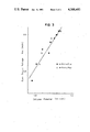
- FIG. 3 is a graph showing the relation between the diffusion potential, Vd, and the open circuit voltage as obtained with the p type amorphous semiconductor on the window side.
- the amorphous silicon of this invention is obtained by subjecting a mixed gas consisting of silane (SiH 4 ) or a derivative thereof, silane fluoride or a derivative thereof, or a mixture thereof and an inert gas such as hydrogen, argon diluted with hydrogen or helium to radio-frequency glow decomposition or DC glow discharge decomposition by the capacitive or inductive coupling method.
- concentration of silane in the mixed gas generally is in the range of from 0.5 to 50%, preferably in the range of from 1 to 20%.
- the substrate is desired to have a working temperature in the range of from 200° to 300° C. It comprises a glass sheet having a transparent electrode (such as of ITO and SnO 2 ) vacuum deposited thereon, a polymer film, or a metal sheet and having all other component layers indispensable to the construction of a solar cell.
- a transparent electrode such as of ITO and SnO 2
- FIGS. 1(a), (b) Typical examples of the basic construction of a solar cell as shown in FIGS. 1(a), (b). Illustrated in (a) is the type wherein the light impinges on the p side. This type has a construction of Glass - transparent electrode - p - i - n - Al, for example. Illustrated in (b) is the type wherein the light impinges on the n side. This type has a construction of stainless steel - p - i - n - transparent electrode. Optionally, other constructions may be formed by interposing a thin insulation layer or a thin metal layer between the p layer and the transparent electrode. Any construction suffices so far as the p-i-n junction is included as the basic component.
- the p-i-n junction is constructed by forming an i layer of intrinsic amorphous silicon (hereinafter referred to as i type a-Si) obtained by the glow discharge decomposition of silane or a derivative thereof, silane fluoride or a derivative thereof or a mixture thereof and possessed of a carrier lifetime of not less than about 10 -7 second, localized density states of not more than about 10 17 cm -3 eV -1 , and a mobility of not less than 10 -3 cm 2 /V and by joining p and n type doped semiconductors to the i layer.
- i type a-Si intrinsic amorphous silicon
- the construction contemplated by this invention is characterized by using, as either the p or n layer, on which the light impinges, an amorphous semiconductor having an optical band gap of not less than about 1.85 eV, an electric conductivity of not less than about 10 -8 ( ⁇ .cm) -1 at 20° C. and a diffusion potential, Vd, (exhibited in the p-i-n junction) of not less than about 1.1 volts.
- p or n type amorphous semiconductors having the above properties may be used in each of the p and n layers.
- this layer may contain an element of Group III of the Periodic Table of Elements, e.g., when a-Si (as in the i-type layer) or an element of Group V of the same table when a-Si is doped to produce an n type layer.
- the amorphous semiconductor of this invention is made of amorphous silicon carbide or amorphous silicon nitride represented by the general formula, a-Si 1-x C x or a-Si 1-y N y . These compounds are obtained by subjecting a hydrogen or fluorine compound of silicon and a hydrogen or fluorine compound of carbon or a hydrogen-nitrogen compound, such as NH 3 gas, hydrazine, etc. to glow discharge decomposition.
- Hydrogen and fluorine play an important role in amorphous silicon carbide. They are considered to act as terminators for dangling bonds in amorphous silicon obtained by the glow discharge decomposition of silane or silane fluoride.
- concentration of hydrogen and/or fluorine in a film of amorphous silicon carbide depends largely on the substrate temperature, and other conditions of manufacture. According to this invention, the film contains about 3 to 30 atom % of hydrogen and/or fluorine, since the substrate temperature is preferably in the range of 200° C. to 350° C.
- any amorphous semiconductor may be used on condition that it be possessed of an optical band gap of not less than about 1.85 eV, an electric conductivity of not less than about 10 -8 ( ⁇ .cm) -1 , usually not more than 10° ( ⁇ .cm) -1 at 20° C. and a diffusion potential, Vd, (exhibited in the pin junction) of not less than about 1.1 volts.
- the amorphous semiconductor of the foregoing description has a large optical band gap and exhibits a very high open voltage, Voc, even though the semiconductor, when used as the window material for the pin junction photovoltaic cell, naturally has a possibility of increasing the short-circuit current, Jsc. It has been found that in the photovoltaic cell of this invention, there exists a correlation between the diffusion potential, Vd and the open circuit voltage of the cell as depicted by the band profile of FIG. 2. Although the diffusion potential, Vd, in the case of this invention exceeds about 1.1 volts, the trend of the relation is nearly constant without reference to the kind of the amorphous semiconductor to be used on the side exposed to the incident light.
- This diffusion potential is the difference obtained by subtracting the Fermi level, E f , of the p, n doped layers from the optical band gap, Eg.opt, of the amorphous semiconductor on the side exposed to the light.
- E f the Fermi level
- Eg.opt the optical band gap
- the diffusion potential is similarly obtained by subtracting the Fermi level, Ef, of the p, n layers from the optical band gap, Eg.opt, of the n type amorphous semiconductor.
- This invention requires the optical band gap, Eg.opt, to be at least about 1.85 eV and the diffusion potential, Vd, to be at least about 1.1 volts.
- the heterojunction photovoltaic cell provides a great improvement in short-circuit current, Jsc, and open circuit voltage, Voc.
- This invention further requires the electric conductivity to be at least 10 -8 ( ⁇ .cm) -1 at room temperature.
- the reason for this lower limit is that below this limit, the fill factor, FF, becomes too small for the conversion efficiency to be practical.
- the cell is composed of a transparent electrode - p type amorphous semiconductor - i type a-Si - n type a-Si - electrode, with the transparent electrode side designed to be exposed to the incident light.
- the transparent electrode is desirably formed of ITO or SnO 2 , preferably the latter. It may be formed by having this substance vacuum deposited on a glass substrate or by having the substance directly vacuum deposited on the p type amorphous semiconductor.
- the p type amorphous semiconductor on the side of the cell exposed to the incident light is desired to have a thickness in the range of from about 30 A to 300 A, preferably from 50 A to 200 A.
- the thickness of the i type a-Si layer is not specifically limited in the cell of this invention, it is generally selected within the range of from about 2500 A to 10,000 A.
- the n type a-Si layer whose primary function is to establish ohmic contact has no particular thickness limitation. Generally, the thickness of this layer is selected in the range of from about 150 A to 600 A.
- this n type a-Si layer may be substituted by an n type amorphous semiconductor of this invention.
- the cell is composed of a transparent electrode - n type amorphous semiconductor - i type a-Si - p type a-Si - electrode, with the transparent electrode side to be exposed to the incident light.
- the n type amorphous semiconductor on the side of the cell exposed to the incident light desirably has a thickness in the range of from about 30 A to 300 A, preferably from 50 A to 200 A.
- the thickness of the i type a-Si is not specifically limited, it is generally selected in the range of from about 2500 A to 10,000 A.
- the thickness of the p type a-Si layer which is not particularly limited either, is generally selected in the range of from about 150 A to 600 A.
- this p type a-Si layer may be substituted by a p type amorphous semiconductor of the present invention.
- the material for the transparent electrode and the method for the vacuum deposition thereof are the same as described above.
- Glow discharge decomposition was performed at a high frequency of 14.56 MHz in a quartz test tube having an inside diameter of 11 cm.
- An i type a-Si layer was obtained by subjecting silane diluted with hydrogen to the glow discharge decomposition at 2 to 10 Torrs.
- the gas composition involved in the glow discharge decomposition was adjusted so that the atomic fraction y in the formula, a-Si 1-y N y , would fall in the range of from 0.75 to 0.05.
- a solar cell was constructed by successively depositing the p type a-Si 1-y N y , the i type a-Si and the n type a-Si in the order mentioned on the SnO 2 surface of a glass substrate coated with an SnO 2 film of 25 ⁇ / ⁇ and finally vacuum depositing aluminum of 3.3 mm 2 .
- This solar cell was tested for cell properties by use of a solar simulator of AM-1 (100 mW/cm 2 ). During the glow discharge, the temperature of the substrate was kept at 250° C. The thickness of the i layer was 5000 A, that of the n layer 500 A, and that of the p type a-Si 1-y N y layer 135 A.
- the solar cell properties vs. varying compositions of the p type a-Si 1-y N y film are shown in Table 1. It is seen from this table that the conversion coefficient (hereinafter represented by " ⁇ ") which is 4.6% for the layer formed solely of silane (Si 1 N 0 ) is increased to 5.45%, 6.5% and 6.75 respectively when the value of "y" in the formula, a-Si 1-y N y , of this invention is 0.05, 0.20 and 0.40, indicating that the n type amorphous semiconductor of this invention permits a conspicuous improvement in the value of ⁇ .
- ⁇ the conversion coefficient which is 4.6% for the layer formed solely of silane (Si 1 N 0 ) is increased to 5.45%, 6.5% and 6.75 respectively when the value of "y" in the formula, a-Si 1-y N y , of this invention is 0.05, 0.20 and 0.40, indicating that the n type amorphous semiconductor of this invention permits a conspicuous improvement in the value of
- the conversion efficiency begins to show a sign of decline as the value of "y" exceeds 0.5, because the increase in the resistance offered by the p type a-Si 1-y N y reaches a point where the fill factor (hereinafter referred to as FF) falls.
- the short-circuit current (hereinafter referred to as Jsc) and the open voltage (hereinafter referred to as Voc) remain substantially unaffected.
- Jsc short-circuit current
- Voc open voltage
- the solar cell properties vs. varying compositions of the p type a-Si 1-x C x are shown in Table 2. The results reveal the conspicuous improvement brought about in Jsc and Voc values.
- the values of the optical band gap, Eg.opt, of the a-Si 1-x C x and the a-Si 1-y N y are greater than the value of a-Si as shown in Tables 1, 2.
- Use of these amorphous semiconductors as window materials therefore, is naturally expected to bring about an improvement in the Jsc properties. Moreover, it brings about an unexpected conspicuous improvement in the Voc properties, which leads to a great enhancement of the conversion efficiency.
- this invention has issued from the discovery that the heterojunction photovoltaic cell which uses as the window material the amorphous semiconductor having an Eg.opt of at least about 1.85 eV and a pin junction diffusion potential, Vd, of at least 1.1 volts enjoys a conspicuous improvement in not only Jsc but also Voc. Surprisingly, this effect of the invention does not depend on the type of the amorphous semiconductor. The effect described above is entirely the same when the n type amorphous semiconductor of the cell is exposed to the incident light.
Abstract
Description
                                  TABLE 1
__________________________________________________________________________
p type a-Si.sub.(1-y) N.sub.(y) /i-n a-Si:H
__________________________________________________________________________
Atomic Fraction (y)
                0    0.05 0.10 0.20 0.30 0.40 0.50 0.70
Eg. opt (eV)    1.76 1.81 1.85 1.92 2.01 2.11 2.20 2.27
Electric Conductivity (Ω · cm).sup.-1
                5 × 10.sup.-7
                     4 × 10.sup.-7
                          5 × 10.sup.-7
                               5 × 10.sup.-7
                                    3 × 10.sup.-7
                                         2 × 10.sup.-7
                                              1 × 10.sup.-7
                                                   8 × 10.sup.-8
Ef-Ev (eV)      0.6  0.55 0.56 0.50 0.51 0.56 0.67 0.75
Vd (volts)      0.96 1.06 1.09 1.22 1.30 1.35 1.33 1.32
Solar Cell
        Jsc (mA/cm.sup.2)
                10.3 10.8 11.2 11.6 11.9 12.15
                                              12.1 12.2
Properties
        Voc (volts)
                0.75 0.82 0.85 0.89 0.90 0.91 0.91 0.91
        FF      0.60 0.615
                          0.62 0.63 0.62 0.61 0.59 0.57
        η(%)
                4.6  5.45 5.9  6.5  6.6  6.75 6.50 6.30
__________________________________________________________________________
                                  TABLE 2
__________________________________________________________________________
p type a-Si.sub.(1-x) C.sub.x /i-n a-Si:H
__________________________________________________________________________
Atomic Fraction (x)
                 0    0.05 0.1  0.2  0.3  0.4  0.5  0.7  0.85
Eg. opt (eV)     1.76 1.80 1.85 1.95 2.06 2.10 2.11 2.10 2.09
Electric Conductivity (Ω · cm).sup.-1
                 5 × 10.sup.-7
                      7 × 10.sup.-7
                           7 × 10.sup.-7
                                1 × 10.sup.-6
                                     8 × 10.sup.-7
                                          6 × 10.sup.-7
                                               3 × 10.sup.-7
                                                    2 × 10.sup.-7
                                                         9 ×
                                                         10.sup.-8
Ef-Ev (eV)       0.6  0.58 0.55 0.54 0.57 0.57 0.65 0.65 0.70
Vd (volts)       0.96 1.02 1.10 1.21 1.29 1.33 1.26 1.25 1.19
Solar Cell
        Jsc (mA/cm.sup.2)
                 10.0 10.3 10.8 11.5 11.9 12.0 12.1 12.0 11.9
Properties
        Voc (volts)
                 0.75 0.82 0.86 0.88 0.90 0.91 0.89 0.885
                                                         0.85
        FF       0.61 0.64 0.68 0.70 0.67 0.66 0.66 0.62 0.58
        η(%) 4.6  5.4  6.3  7.1  7.18 7.2  7.1  6.6  5.9
__________________________________________________________________________
 i 1Si:H Eg. opt = 1.8eV
 EcEf = 0.85eV
 n type aSi:H Eg. opt = 1.8eV
 EcEf = 0.2eV
Claims (13)
Applications Claiming Priority (6)
| Application Number | Priority Date | Filing Date | Title |
|---|---|---|---|
| JP56012313A JPS57126175A (en) | 1981-01-29 | 1981-01-29 | Amorphous silicon carbide/amorophous silicon hetero junction optoelectric element |
| JP56-12313 | 1981-01-29 | ||
| JP56-22690 | 1981-02-17 | ||
| JP56022690A JPS57136377A (en) | 1981-02-17 | 1981-02-17 | Amorphous silicon nitride/amorphous silicon heterojunction photoelectric element |
| JP56-66689 | 1981-04-30 | ||
| JP56066689A JPS57181176A (en) | 1981-04-30 | 1981-04-30 | High voltage amorphous semiconductor/amorphous silicon hetero junction photosensor |
Publications (1)
| Publication Number | Publication Date |
|---|---|
| US4388482A true US4388482A (en) | 1983-06-14 |
Family
ID=27279788
Family Applications (1)
| Application Number | Title | Priority Date | Filing Date |
|---|---|---|---|
| US06/266,064 Expired - Lifetime US4388482A (en) | 1981-01-29 | 1981-05-19 | High-voltage photovoltaic cell having a heterojunction of amorphous semiconductor and amorphous silicon |
Country Status (1)
| Country | Link |
|---|---|
| US (1) | US4388482A (en) |
Cited By (37)
| Publication number | Priority date | Publication date | Assignee | Title |
|---|---|---|---|---|
| US4476346A (en) * | 1982-12-14 | 1984-10-09 | Kanegafuchi Kagaku Kogyo Kabushiki Kaisha | Photovoltaic device |
| US4499331A (en) * | 1981-07-17 | 1985-02-12 | Kanegafuchi Kagaku Kogyo Kabushiki Kaisha | Amorphous semiconductor and amorphous silicon photovoltaic device |
| US4525437A (en) * | 1982-03-29 | 1985-06-25 | Semiconductor Energy Laboratory Co., Ltd. | Light energy conversion system |
| US4525435A (en) * | 1982-03-29 | 1985-06-25 | Semiconductor Energy Laboratory Co., Ltd. | Light energy conversion system |
| US4528418A (en) * | 1984-02-24 | 1985-07-09 | Energy Conversion Devices, Inc. | Photoresponsive semiconductor device having a double layer anti-reflective coating |
| US4542255A (en) * | 1984-01-03 | 1985-09-17 | Atlantic Richfield Company | Gridded thin film solar cell |
| US4581625A (en) * | 1983-12-19 | 1986-04-08 | Atlantic Richfield Company | Vertically integrated solid state color imager |
| US4582770A (en) * | 1980-06-25 | 1986-04-15 | Shunpei Yamazaki | Printing member for electrostatic photocopying |
| US4582721A (en) * | 1981-05-29 | 1986-04-15 | Kanegafuchi Kagaku Kogyo Kabushiki Kaisha | Process for preparing amorphous silicon semiconductor |
| US4584427A (en) * | 1984-10-22 | 1986-04-22 | Atlantic Richfield Company | Thin film solar cell with free tin on tin oxide transparent conductor |
| US4589194A (en) * | 1983-12-29 | 1986-05-20 | Atlantic Richfield Company | Ultrasonic scribing of thin film solar cells |
| US4613880A (en) * | 1981-08-19 | 1986-09-23 | Sanyo Electric Co., Ltd. | Light sensitive apparatus |
| EP0204562A2 (en) * | 1985-06-04 | 1986-12-10 | Siemens Solar Industries L.P. | Transparent photovoltaic module |
| US4776894A (en) * | 1986-08-18 | 1988-10-11 | Sanyo Electric Co., Ltd. | Photovoltaic device |
| US4790883A (en) * | 1987-12-18 | 1988-12-13 | Porponth Sichanugrist | Low light level solar cell |
| US4889783A (en) * | 1980-06-25 | 1989-12-26 | Semiconductor Energy Laboratory Co., Ltd. | Printing member for electrostatic photocopying |
| US4889782A (en) * | 1980-06-25 | 1989-12-26 | Semiconductor Energy Laboratory Co., Ltd. | Electrostatic photocopying machine |
| US4971872A (en) * | 1980-06-25 | 1990-11-20 | Shunpei Yamazaki | Electrostatic photocopying machine |
| US4999270A (en) * | 1980-06-25 | 1991-03-12 | Semiconductor Energy Laboratory Co., Ltd. | Printing member for electrostatic photocopying |
| US5008171A (en) * | 1980-06-25 | 1991-04-16 | Semiconductor Energy Laboratory Co., Ltd. | Printing member for electrostatic photocopying |
| US5053844A (en) * | 1988-05-13 | 1991-10-01 | Ricoh Company, Ltd. | Amorphous silicon photosensor |
| US5103262A (en) * | 1980-06-25 | 1992-04-07 | Semiconductor Energy Laboratory Co., Ltd. | Printing member for electrostatic photocopying |
| US5144367A (en) * | 1980-06-25 | 1992-09-01 | Semiconductor Energy Laboratory Co., Ltd. | Printing member for electrostatic photocopying |
| US5143808A (en) * | 1980-06-25 | 1992-09-01 | Semiconductor Energy Laboratory Co., Ltd. | Printing member for electrostatic photocopying |
| US5238866A (en) * | 1991-09-11 | 1993-08-24 | GmbH & Co. Ingenieurburo Berlin Biotronik Mess- und Therapiegerate | Plasma enhanced chemical vapor deposition process for producing an amorphous semiconductive surface coating |
| USRE35198E (en) * | 1978-03-03 | 1996-04-02 | Canon Kabushiki Kaisha | Image forming member for electrophotography |
| US5545503A (en) * | 1980-06-25 | 1996-08-13 | Semiconductor Energy Laboratory Co., Ltd. | Method of making printing member for electrostatic photocopying |
| US20090093080A1 (en) * | 2007-07-10 | 2009-04-09 | Soo Young Choi | Solar cells and methods and apparatuses for forming the same including i-layer and n-layer chamber cleaning |
| US20100059110A1 (en) * | 2008-09-11 | 2010-03-11 | Applied Materials, Inc. | Microcrystalline silicon alloys for thin film and wafer based solar applications |
| US20100170565A1 (en) * | 2007-12-26 | 2010-07-08 | Mitsubishi Heavy Industries, Ltd. | Photovoltaic device and method for producing the same |
| US20100227431A1 (en) * | 2009-03-03 | 2010-09-09 | Applied Materials, Inc. | Crystalline silicon solar cells on low purity substrate |
| US20110000545A1 (en) * | 2009-07-03 | 2011-01-06 | Semiconductor Energy Laboratory Co., Ltd. | Photoelectric Conversion Device and Manufacturing Method Thereof |
| WO2011070104A1 (en) | 2009-12-11 | 2011-06-16 | Laurent Sigler | Organic photovoltaic cell |
| US20140116501A1 (en) * | 2012-10-26 | 2014-05-01 | Stmicroelectronics S.R.I. | Photovoltaic cell |
| US8940576B1 (en) * | 2011-09-22 | 2015-01-27 | Hrl Laboratories, Llc | Methods for n-type doping of graphene, and n-type-doped graphene compositions |
| US8994009B2 (en) | 2011-09-07 | 2015-03-31 | Semiconductor Energy Laboratory Co., Ltd. | Photoelectric conversion device |
| US9437758B2 (en) | 2011-02-21 | 2016-09-06 | Semiconductor Energy Laboratory Co., Ltd. | Photoelectric conversion device |
Citations (1)
| Publication number | Priority date | Publication date | Assignee | Title |
|---|---|---|---|---|
| US4109271A (en) * | 1977-05-27 | 1978-08-22 | Rca Corporation | Amorphous silicon-amorphous silicon carbide photovoltaic device |
-
1981
- 1981-05-19 US US06/266,064 patent/US4388482A/en not_active Expired - Lifetime
Patent Citations (1)
| Publication number | Priority date | Publication date | Assignee | Title |
|---|---|---|---|---|
| US4109271A (en) * | 1977-05-27 | 1978-08-22 | Rca Corporation | Amorphous silicon-amorphous silicon carbide photovoltaic device |
Cited By (50)
| Publication number | Priority date | Publication date | Assignee | Title |
|---|---|---|---|---|
| USRE35198E (en) * | 1978-03-03 | 1996-04-02 | Canon Kabushiki Kaisha | Image forming member for electrophotography |
| US5103262A (en) * | 1980-06-25 | 1992-04-07 | Semiconductor Energy Laboratory Co., Ltd. | Printing member for electrostatic photocopying |
| US5545503A (en) * | 1980-06-25 | 1996-08-13 | Semiconductor Energy Laboratory Co., Ltd. | Method of making printing member for electrostatic photocopying |
| US5303007A (en) * | 1980-06-25 | 1994-04-12 | Semiconductor Energy Laboratory Co., Ltd. | Printing apparatus for electrostatic photocopying |
| US5143808A (en) * | 1980-06-25 | 1992-09-01 | Semiconductor Energy Laboratory Co., Ltd. | Printing member for electrostatic photocopying |
| US5144367A (en) * | 1980-06-25 | 1992-09-01 | Semiconductor Energy Laboratory Co., Ltd. | Printing member for electrostatic photocopying |
| US4598031A (en) * | 1980-06-25 | 1986-07-01 | Shunpei Yamazaki | Printing member for electrostatic photocopying |
| US5008171A (en) * | 1980-06-25 | 1991-04-16 | Semiconductor Energy Laboratory Co., Ltd. | Printing member for electrostatic photocopying |
| US4999270A (en) * | 1980-06-25 | 1991-03-12 | Semiconductor Energy Laboratory Co., Ltd. | Printing member for electrostatic photocopying |
| US4971872A (en) * | 1980-06-25 | 1990-11-20 | Shunpei Yamazaki | Electrostatic photocopying machine |
| US4582770A (en) * | 1980-06-25 | 1986-04-15 | Shunpei Yamazaki | Printing member for electrostatic photocopying |
| US4889782A (en) * | 1980-06-25 | 1989-12-26 | Semiconductor Energy Laboratory Co., Ltd. | Electrostatic photocopying machine |
| US4889783A (en) * | 1980-06-25 | 1989-12-26 | Semiconductor Energy Laboratory Co., Ltd. | Printing member for electrostatic photocopying |
| US4587187A (en) * | 1980-06-25 | 1986-05-06 | Shunpei Yamazaki | Printing member for electrostatic photocopying |
| US4582721A (en) * | 1981-05-29 | 1986-04-15 | Kanegafuchi Kagaku Kogyo Kabushiki Kaisha | Process for preparing amorphous silicon semiconductor |
| US4499331A (en) * | 1981-07-17 | 1985-02-12 | Kanegafuchi Kagaku Kogyo Kabushiki Kaisha | Amorphous semiconductor and amorphous silicon photovoltaic device |
| US4613880A (en) * | 1981-08-19 | 1986-09-23 | Sanyo Electric Co., Ltd. | Light sensitive apparatus |
| US4525435A (en) * | 1982-03-29 | 1985-06-25 | Semiconductor Energy Laboratory Co., Ltd. | Light energy conversion system |
| US4525436A (en) * | 1982-03-29 | 1985-06-25 | Semiconductor Energy Laboratory Co., Ltd. | Light energy conversion system |
| US4525437A (en) * | 1982-03-29 | 1985-06-25 | Semiconductor Energy Laboratory Co., Ltd. | Light energy conversion system |
| US4528252A (en) * | 1982-03-29 | 1985-07-09 | Semiconductor Energy Laboratory Co., Ltd. | Light energy conversion system |
| US4476346A (en) * | 1982-12-14 | 1984-10-09 | Kanegafuchi Kagaku Kogyo Kabushiki Kaisha | Photovoltaic device |
| US4581625A (en) * | 1983-12-19 | 1986-04-08 | Atlantic Richfield Company | Vertically integrated solid state color imager |
| US4589194A (en) * | 1983-12-29 | 1986-05-20 | Atlantic Richfield Company | Ultrasonic scribing of thin film solar cells |
| US4542255A (en) * | 1984-01-03 | 1985-09-17 | Atlantic Richfield Company | Gridded thin film solar cell |
| EP0154451A2 (en) * | 1984-02-24 | 1985-09-11 | Energy Conversion Devices, Inc. | Photoresponsive semiconductor device having a double layer anti-reflective coating |
| US4528418A (en) * | 1984-02-24 | 1985-07-09 | Energy Conversion Devices, Inc. | Photoresponsive semiconductor device having a double layer anti-reflective coating |
| EP0154451A3 (en) * | 1984-02-24 | 1986-09-17 | Energy Conversion Devices, Inc. | Photoresponsive semiconductor device having a double layer anti-reflective coating |
| US4584427A (en) * | 1984-10-22 | 1986-04-22 | Atlantic Richfield Company | Thin film solar cell with free tin on tin oxide transparent conductor |
| EP0204562A2 (en) * | 1985-06-04 | 1986-12-10 | Siemens Solar Industries L.P. | Transparent photovoltaic module |
| EP0204562A3 (en) * | 1985-06-04 | 1989-05-03 | Siemens Solar Industries L.P. | Transparent photovoltaic module |
| US4776894A (en) * | 1986-08-18 | 1988-10-11 | Sanyo Electric Co., Ltd. | Photovoltaic device |
| US4790883A (en) * | 1987-12-18 | 1988-12-13 | Porponth Sichanugrist | Low light level solar cell |
| US5053844A (en) * | 1988-05-13 | 1991-10-01 | Ricoh Company, Ltd. | Amorphous silicon photosensor |
| US5238866A (en) * | 1991-09-11 | 1993-08-24 | GmbH & Co. Ingenieurburo Berlin Biotronik Mess- und Therapiegerate | Plasma enhanced chemical vapor deposition process for producing an amorphous semiconductive surface coating |
| US7875486B2 (en) | 2007-07-10 | 2011-01-25 | Applied Materials, Inc. | Solar cells and methods and apparatuses for forming the same including I-layer and N-layer chamber cleaning |
| US20090093080A1 (en) * | 2007-07-10 | 2009-04-09 | Soo Young Choi | Solar cells and methods and apparatuses for forming the same including i-layer and n-layer chamber cleaning |
| US20100170565A1 (en) * | 2007-12-26 | 2010-07-08 | Mitsubishi Heavy Industries, Ltd. | Photovoltaic device and method for producing the same |
| US20100059110A1 (en) * | 2008-09-11 | 2010-03-11 | Applied Materials, Inc. | Microcrystalline silicon alloys for thin film and wafer based solar applications |
| US20100227431A1 (en) * | 2009-03-03 | 2010-09-09 | Applied Materials, Inc. | Crystalline silicon solar cells on low purity substrate |
| US7858427B2 (en) | 2009-03-03 | 2010-12-28 | Applied Materials, Inc. | Crystalline silicon solar cells on low purity substrate |
| US20110000545A1 (en) * | 2009-07-03 | 2011-01-06 | Semiconductor Energy Laboratory Co., Ltd. | Photoelectric Conversion Device and Manufacturing Method Thereof |
| US9496428B2 (en) | 2009-07-03 | 2016-11-15 | Semiconductor Energy Laboratory Co., Ltd. | Photoelectric conversion device and manufacturing method thereof |
| WO2011070104A1 (en) | 2009-12-11 | 2011-06-16 | Laurent Sigler | Organic photovoltaic cell |
| US9437758B2 (en) | 2011-02-21 | 2016-09-06 | Semiconductor Energy Laboratory Co., Ltd. | Photoelectric conversion device |
| US8994009B2 (en) | 2011-09-07 | 2015-03-31 | Semiconductor Energy Laboratory Co., Ltd. | Photoelectric conversion device |
| US8940576B1 (en) * | 2011-09-22 | 2015-01-27 | Hrl Laboratories, Llc | Methods for n-type doping of graphene, and n-type-doped graphene compositions |
| US20140116501A1 (en) * | 2012-10-26 | 2014-05-01 | Stmicroelectronics S.R.I. | Photovoltaic cell |
| US10128396B2 (en) * | 2012-10-26 | 2018-11-13 | Stmicroelectronics S.R.L. | Photovoltaic cell |
| US11257975B2 (en) * | 2012-10-26 | 2022-02-22 | Stmicroelectronics S.R.L. | Photovoltaic cell |
Similar Documents
| Publication | Publication Date | Title |
|---|---|---|
| US4388482A (en) | High-voltage photovoltaic cell having a heterojunction of amorphous semiconductor and amorphous silicon | |
| US4499331A (en) | Amorphous semiconductor and amorphous silicon photovoltaic device | |
| US5646050A (en) | Increasing stabilized performance of amorphous silicon based devices produced by highly hydrogen diluted lower temperature plasma deposition | |
| US8030120B2 (en) | Hybrid window layer for photovoltaic cells | |
| US4385200A (en) | Photovoltaic cell having a hetero junction of amorphous silicon carbide and amorphous silicon | |
| US20080173347A1 (en) | Method And Apparatus For A Semiconductor Structure | |
| Hegedus et al. | Current transport in amorphous silicon n/p junctions and their application as ‘‘tunnel’’junctions in tandem solar cells | |
| EP0053402B1 (en) | Pin photovoltaic cell having a hetero junction of amorphous siliconcompound and amorphous silicon | |
| JP3248227B2 (en) | Thin film solar cell and method of manufacturing the same | |
| Tsuda et al. | a-Si technologies for high efficiency solar cells | |
| JPH0544198B2 (en) | ||
| JPH0340515B2 (en) | ||
| JPH0122991B2 (en) | ||
| Wagner | Physical aspects and technological realization of amorphous silicon thin film solar cells | |
| JP3245962B2 (en) | Manufacturing method of thin film solar cell | |
| JPH0719906B2 (en) | Method for manufacturing semiconductor device | |
| JPH0554272B2 (en) | ||
| Liao et al. | High efficiency amorphous silicon germanium solar cells | |
| JP2545066B2 (en) | Semiconductor device | |
| JP3025122B2 (en) | Photovoltaic element and power generation system | |
| Tanaka et al. | Fabricating high performance a-Si solar cells by alternately repeating deposition and hydrogen plasma treatment method | |
| JPH06181329A (en) | Photovoltaic element and generating system | |
| JP2836717B2 (en) | Photovoltaic element and power generation system | |
| JPH03188682A (en) | High potential amorphous semiconductor/amorphous silicon heterojunction photovoltaic element | |
| GB2319662A (en) | Amorphous Silicon Solar Cell |
Legal Events
| Date | Code | Title | Description |
|---|---|---|---|
| STCF | Information on status: patent grant |
Free format text: PATENTED CASE |
|
| AS | Assignment |
Owner name: KANEGAFUCHI KAGAKU KOGYO KABUSHIKI KAISHA NO. 2-4 Free format text: ASSIGNMENT OF ASSIGNORS INTEREST.;ASSIGNORS:HAMAKAWA, YOSHIHIRO;TAWADA, YOSHIHISA;REEL/FRAME:004301/0466 Effective date: 19840816 |
|
| MAFP | Maintenance fee payment |
Free format text: PAYMENT OF MAINTENANCE FEE, 4TH YEAR, PL 96-517 (ORIGINAL EVENT CODE: M170); ENTITY STATUS OF PATENT OWNER: LARGE ENTITY Year of fee payment: 4 |
|
| FEPP | Fee payment procedure |
Free format text: PAYMENT IS IN EXCESS OF AMOUNT REQUIRED. REFUND SCHEDULED (ORIGINAL EVENT CODE: F169); ENTITY STATUS OF PATENT OWNER: LARGE ENTITY |
|
| MAFP | Maintenance fee payment |
Free format text: PAYMENT OF MAINTENANCE FEE, 8TH YEAR, PL 96-517 (ORIGINAL EVENT CODE: M171); ENTITY STATUS OF PATENT OWNER: LARGE ENTITY Year of fee payment: 8 |
|
| FEPP | Fee payment procedure |
Free format text: PAYOR NUMBER ASSIGNED (ORIGINAL EVENT CODE: ASPN); ENTITY STATUS OF PATENT OWNER: LARGE ENTITY |
|
| FEPP | Fee payment procedure |
Free format text: PAYOR NUMBER ASSIGNED (ORIGINAL EVENT CODE: ASPN); ENTITY STATUS OF PATENT OWNER: LARGE ENTITY Free format text: PAYER NUMBER DE-ASSIGNED (ORIGINAL EVENT CODE: RMPN); ENTITY STATUS OF PATENT OWNER: LARGE ENTITY |
|
| MAFP | Maintenance fee payment |
Free format text: PAYMENT OF MAINTENANCE FEE, 12TH YEAR, LARGE ENTITY (ORIGINAL EVENT CODE: M185); ENTITY STATUS OF PATENT OWNER: LARGE ENTITY Year of fee payment: 12 |