US4411058A - Process for fabricating CMOS devices with self-aligned channel stops - Google Patents
Process for fabricating CMOS devices with self-aligned channel stops Download PDFInfo
- Publication number
- US4411058A US4411058A US06/297,903 US29790381A US4411058A US 4411058 A US4411058 A US 4411058A US 29790381 A US29790381 A US 29790381A US 4411058 A US4411058 A US 4411058A
- Authority
- US
- United States
- Prior art keywords
- channel
- regions
- layer
- thick
- metal layer
- Prior art date
- Legal status (The legal status is an assumption and is not a legal conclusion. Google has not performed a legal analysis and makes no representation as to the accuracy of the status listed.)
- Expired - Lifetime
Links
- 238000000034 method Methods 0.000 title claims abstract description 53
- 239000000758 substrate Substances 0.000 claims abstract description 45
- 239000004065 semiconductor Substances 0.000 claims abstract description 19
- 230000000295 complement effect Effects 0.000 claims abstract description 16
- 238000004519 manufacturing process Methods 0.000 claims abstract description 4
- 229910052751 metal Inorganic materials 0.000 claims description 43
- 239000002184 metal Substances 0.000 claims description 43
- 239000002131 composite material Substances 0.000 claims description 31
- 229920002120 photoresistant polymer Polymers 0.000 claims description 29
- 229910021420 polycrystalline silicon Inorganic materials 0.000 claims description 22
- 229920005591 polysilicon Polymers 0.000 claims description 21
- 150000002500 ions Chemical class 0.000 claims description 17
- VYPSYNLAJGMNEJ-UHFFFAOYSA-N Silicium dioxide Chemical compound O=[Si]=O VYPSYNLAJGMNEJ-UHFFFAOYSA-N 0.000 claims description 14
- 239000010703 silicon Substances 0.000 claims description 13
- ZOXJGFHDIHLPTG-UHFFFAOYSA-N Boron Chemical group [B] ZOXJGFHDIHLPTG-UHFFFAOYSA-N 0.000 claims description 12
- 229910052710 silicon Inorganic materials 0.000 claims description 12
- 125000004429 atom Chemical group 0.000 claims description 10
- XAGFODPZIPBFFR-UHFFFAOYSA-N aluminium Chemical compound [Al] XAGFODPZIPBFFR-UHFFFAOYSA-N 0.000 claims description 8
- 229910052782 aluminium Inorganic materials 0.000 claims description 7
- 239000000377 silicon dioxide Substances 0.000 claims description 7
- 238000009826 distribution Methods 0.000 claims description 6
- 125000004437 phosphorous atom Chemical group 0.000 claims description 5
- 235000012239 silicon dioxide Nutrition 0.000 claims description 5
- 238000001704 evaporation Methods 0.000 claims description 4
- 239000010931 gold Substances 0.000 claims description 4
- PCHJSUWPFVWCPO-UHFFFAOYSA-N gold Chemical compound [Au] PCHJSUWPFVWCPO-UHFFFAOYSA-N 0.000 claims description 3
- 229910052737 gold Inorganic materials 0.000 claims description 3
- 238000000151 deposition Methods 0.000 claims description 2
- 238000001465 metallisation Methods 0.000 claims description 2
- 229910044991 metal oxide Inorganic materials 0.000 abstract description 2
- 150000004706 metal oxides Chemical class 0.000 abstract description 2
- 239000010410 layer Substances 0.000 description 47
- 108091006146 Channels Proteins 0.000 description 26
- XUIMIQQOPSSXEZ-UHFFFAOYSA-N Silicon Chemical compound [Si] XUIMIQQOPSSXEZ-UHFFFAOYSA-N 0.000 description 11
- 229910052698 phosphorus Inorganic materials 0.000 description 11
- 239000007943 implant Substances 0.000 description 10
- 239000011574 phosphorus Substances 0.000 description 8
- OAICVXFJPJFONN-UHFFFAOYSA-N Phosphorus Chemical compound [P] OAICVXFJPJFONN-UHFFFAOYSA-N 0.000 description 7
- 229910052796 boron Inorganic materials 0.000 description 7
- 238000005468 ion implantation Methods 0.000 description 7
- 230000015572 biosynthetic process Effects 0.000 description 6
- 238000002513 implantation Methods 0.000 description 5
- -1 boron Chemical class 0.000 description 4
- 230000003071 parasitic effect Effects 0.000 description 4
- 230000000873 masking effect Effects 0.000 description 3
- 229910052785 arsenic Inorganic materials 0.000 description 2
- RQNWIZPPADIBDY-UHFFFAOYSA-N arsenic atom Chemical compound [As] RQNWIZPPADIBDY-UHFFFAOYSA-N 0.000 description 2
- 229910052681 coesite Inorganic materials 0.000 description 2
- 229910052906 cristobalite Inorganic materials 0.000 description 2
- 238000005530 etching Methods 0.000 description 2
- 238000002360 preparation method Methods 0.000 description 2
- 239000002356 single layer Substances 0.000 description 2
- 229910052682 stishovite Inorganic materials 0.000 description 2
- 229910052905 tridymite Inorganic materials 0.000 description 2
- 235000001674 Agaricus brunnescens Nutrition 0.000 description 1
- ZOKXTWBITQBERF-UHFFFAOYSA-N Molybdenum Chemical compound [Mo] ZOKXTWBITQBERF-UHFFFAOYSA-N 0.000 description 1
- 108090000699 N-Type Calcium Channels Proteins 0.000 description 1
- 102000004129 N-Type Calcium Channels Human genes 0.000 description 1
- 108010075750 P-Type Calcium Channels Proteins 0.000 description 1
- 238000010420 art technique Methods 0.000 description 1
- 230000007423 decrease Effects 0.000 description 1
- 230000008021 deposition Effects 0.000 description 1
- 230000000694 effects Effects 0.000 description 1
- 230000008020 evaporation Effects 0.000 description 1
- 229910052732 germanium Inorganic materials 0.000 description 1
- GNPVGFCGXDBREM-UHFFFAOYSA-N germanium atom Chemical compound [Ge] GNPVGFCGXDBREM-UHFFFAOYSA-N 0.000 description 1
- 239000012535 impurity Substances 0.000 description 1
- 230000010354 integration Effects 0.000 description 1
- 239000000463 material Substances 0.000 description 1
- 150000002739 metals Chemical class 0.000 description 1
- 229910052750 molybdenum Inorganic materials 0.000 description 1
- 239000011733 molybdenum Substances 0.000 description 1
- 238000012856 packing Methods 0.000 description 1
- 150000003017 phosphorus Chemical class 0.000 description 1
- 238000001020 plasma etching Methods 0.000 description 1
- 230000000063 preceeding effect Effects 0.000 description 1
- 229910052594 sapphire Inorganic materials 0.000 description 1
- 239000010980 sapphire Substances 0.000 description 1
- 238000000926 separation method Methods 0.000 description 1
- 229910021332 silicide Inorganic materials 0.000 description 1
- FVBUAEGBCNSCDD-UHFFFAOYSA-N silicide(4-) Chemical compound [Si-4] FVBUAEGBCNSCDD-UHFFFAOYSA-N 0.000 description 1
- 229910052814 silicon oxide Inorganic materials 0.000 description 1
- 230000003068 static effect Effects 0.000 description 1
- WFKWXMTUELFFGS-UHFFFAOYSA-N tungsten Chemical compound [W] WFKWXMTUELFFGS-UHFFFAOYSA-N 0.000 description 1
- 229910052721 tungsten Inorganic materials 0.000 description 1
- 239000010937 tungsten Substances 0.000 description 1
Images


Classifications
-
- H—ELECTRICITY
- H01—ELECTRIC ELEMENTS
- H01L—SEMICONDUCTOR DEVICES NOT COVERED BY CLASS H10
- H01L21/00—Processes or apparatus adapted for the manufacture or treatment of semiconductor or solid state devices or of parts thereof
- H01L21/70—Manufacture or treatment of devices consisting of a plurality of solid state components formed in or on a common substrate or of parts thereof; Manufacture of integrated circuit devices or of parts thereof
- H01L21/77—Manufacture or treatment of devices consisting of a plurality of solid state components or integrated circuits formed in, or on, a common substrate
- H01L21/78—Manufacture or treatment of devices consisting of a plurality of solid state components or integrated circuits formed in, or on, a common substrate with subsequent division of the substrate into plural individual devices
- H01L21/82—Manufacture or treatment of devices consisting of a plurality of solid state components or integrated circuits formed in, or on, a common substrate with subsequent division of the substrate into plural individual devices to produce devices, e.g. integrated circuits, each consisting of a plurality of components
- H01L21/822—Manufacture or treatment of devices consisting of a plurality of solid state components or integrated circuits formed in, or on, a common substrate with subsequent division of the substrate into plural individual devices to produce devices, e.g. integrated circuits, each consisting of a plurality of components the substrate being a semiconductor, using silicon technology
- H01L21/8232—Field-effect technology
- H01L21/8234—MIS technology, i.e. integration processes of field effect transistors of the conductor-insulator-semiconductor type
- H01L21/8238—Complementary field-effect transistors, e.g. CMOS
- H01L21/823878—Complementary field-effect transistors, e.g. CMOS isolation region manufacturing related aspects, e.g. to avoid interaction of isolation region with adjacent structure
-
- H—ELECTRICITY
- H01—ELECTRIC ELEMENTS
- H01L—SEMICONDUCTOR DEVICES NOT COVERED BY CLASS H10
- H01L27/00—Devices consisting of a plurality of semiconductor or other solid-state components formed in or on a common substrate
- H01L27/02—Devices consisting of a plurality of semiconductor or other solid-state components formed in or on a common substrate including semiconductor components specially adapted for rectifying, oscillating, amplifying or switching and having at least one potential-jump barrier or surface barrier; including integrated passive circuit elements with at least one potential-jump barrier or surface barrier
- H01L27/04—Devices consisting of a plurality of semiconductor or other solid-state components formed in or on a common substrate including semiconductor components specially adapted for rectifying, oscillating, amplifying or switching and having at least one potential-jump barrier or surface barrier; including integrated passive circuit elements with at least one potential-jump barrier or surface barrier the substrate being a semiconductor body
- H01L27/08—Devices consisting of a plurality of semiconductor or other solid-state components formed in or on a common substrate including semiconductor components specially adapted for rectifying, oscillating, amplifying or switching and having at least one potential-jump barrier or surface barrier; including integrated passive circuit elements with at least one potential-jump barrier or surface barrier the substrate being a semiconductor body including only semiconductor components of a single kind
- H01L27/085—Devices consisting of a plurality of semiconductor or other solid-state components formed in or on a common substrate including semiconductor components specially adapted for rectifying, oscillating, amplifying or switching and having at least one potential-jump barrier or surface barrier; including integrated passive circuit elements with at least one potential-jump barrier or surface barrier the substrate being a semiconductor body including only semiconductor components of a single kind including field-effect components only
- H01L27/088—Devices consisting of a plurality of semiconductor or other solid-state components formed in or on a common substrate including semiconductor components specially adapted for rectifying, oscillating, amplifying or switching and having at least one potential-jump barrier or surface barrier; including integrated passive circuit elements with at least one potential-jump barrier or surface barrier the substrate being a semiconductor body including only semiconductor components of a single kind including field-effect components only the components being field-effect transistors with insulated gate
- H01L27/092—Devices consisting of a plurality of semiconductor or other solid-state components formed in or on a common substrate including semiconductor components specially adapted for rectifying, oscillating, amplifying or switching and having at least one potential-jump barrier or surface barrier; including integrated passive circuit elements with at least one potential-jump barrier or surface barrier the substrate being a semiconductor body including only semiconductor components of a single kind including field-effect components only the components being field-effect transistors with insulated gate complementary MIS field-effect transistors
- H01L27/0928—Devices consisting of a plurality of semiconductor or other solid-state components formed in or on a common substrate including semiconductor components specially adapted for rectifying, oscillating, amplifying or switching and having at least one potential-jump barrier or surface barrier; including integrated passive circuit elements with at least one potential-jump barrier or surface barrier the substrate being a semiconductor body including only semiconductor components of a single kind including field-effect components only the components being field-effect transistors with insulated gate complementary MIS field-effect transistors comprising both N- and P- wells in the substrate, e.g. twin-tub
-
- H—ELECTRICITY
- H01—ELECTRIC ELEMENTS
- H01L—SEMICONDUCTOR DEVICES NOT COVERED BY CLASS H10
- H01L29/00—Semiconductor devices adapted for rectifying, amplifying, oscillating or switching, or capacitors or resistors with at least one potential-jump barrier or surface barrier, e.g. PN junction depletion layer or carrier concentration layer; Details of semiconductor bodies or of electrodes thereof ; Multistep manufacturing processes therefor
- H01L29/02—Semiconductor bodies ; Multistep manufacturing processes therefor
- H01L29/06—Semiconductor bodies ; Multistep manufacturing processes therefor characterised by their shape; characterised by the shapes, relative sizes, or dispositions of the semiconductor regions ; characterised by the concentration or distribution of impurities within semiconductor regions
- H01L29/0603—Semiconductor bodies ; Multistep manufacturing processes therefor characterised by their shape; characterised by the shapes, relative sizes, or dispositions of the semiconductor regions ; characterised by the concentration or distribution of impurities within semiconductor regions characterised by particular constructional design considerations, e.g. for preventing surface leakage, for controlling electric field concentration or for internal isolations regions
- H01L29/0607—Semiconductor bodies ; Multistep manufacturing processes therefor characterised by their shape; characterised by the shapes, relative sizes, or dispositions of the semiconductor regions ; characterised by the concentration or distribution of impurities within semiconductor regions characterised by particular constructional design considerations, e.g. for preventing surface leakage, for controlling electric field concentration or for internal isolations regions for preventing surface leakage or controlling electric field concentration
- H01L29/0638—Semiconductor bodies ; Multistep manufacturing processes therefor characterised by their shape; characterised by the shapes, relative sizes, or dispositions of the semiconductor regions ; characterised by the concentration or distribution of impurities within semiconductor regions characterised by particular constructional design considerations, e.g. for preventing surface leakage, for controlling electric field concentration or for internal isolations regions for preventing surface leakage or controlling electric field concentration for preventing surface leakage due to surface inversion layer, e.g. with channel stopper
-
- Y—GENERAL TAGGING OF NEW TECHNOLOGICAL DEVELOPMENTS; GENERAL TAGGING OF CROSS-SECTIONAL TECHNOLOGIES SPANNING OVER SEVERAL SECTIONS OF THE IPC; TECHNICAL SUBJECTS COVERED BY FORMER USPC CROSS-REFERENCE ART COLLECTIONS [XRACs] AND DIGESTS
- Y10—TECHNICAL SUBJECTS COVERED BY FORMER USPC
- Y10S—TECHNICAL SUBJECTS COVERED BY FORMER USPC CROSS-REFERENCE ART COLLECTIONS [XRACs] AND DIGESTS
- Y10S438/00—Semiconductor device manufacturing: process
- Y10S438/942—Masking
- Y10S438/948—Radiation resist
- Y10S438/95—Multilayer mask including nonradiation sensitive layer
Definitions
- the invention relates to a process for fabricating CMOS devices on a single semiconductor substrate, and, more particularly, to a process for providing CMOS devices with self-aligned channel stops for both n-channel and p-channel devices as well as mutual self-alignment between the two channel stops.
- the two different type channel stops are implanted using only one mask, called herein a "complementary" mask.
- CMOS Complementary Metal Oxide Semiconductor
- CMOS devices formed on a bulk substrate of a given conductivity comprise both NMOS and PMOS devices in adjacent arrangement.
- the source and drain connections of one type of device are of the same conductivity as the substrate, then a well of the opposite conductivity is generally formed in the substrate surrounding the source and drain regions, to which electrical connections are made.
- the source and drain regions are simply implanted into the substrate and electrical connections made thereto.
- a process for fabricating CMOS devices formed on a semiconductor substrate provided with regions of n- and p-type conductivity which includes forming source, drain and gate portions in the regions and making electrical connections to the portions.
- the process comprises forming self-aligned channel stops between regions of the same conductivity and between regions of the opposite conductivity.
- the self-aligned channel stops which are highly doped regions, are formed using one mask (called herein a "complementary" mask). This is accomplished by a process which includes:
- the self-aligned channel stops produce high field threshold voltages for both n- and p-channel devices. Parasitic bipolar transistors are eliminated because heavily doped regions from the channel stop implant do not form the base of a bipolar transistor.
- the mutual self-alignment between the two channel stops provides high packing density because no separation is required between the channel stops for registration tolerance to prevent overlap between p + and n + channel stops. The overlap would otherwise cause compensation of p + and n + species, resulting in a lightly-doped region. Further, the device performance (punch-through voltage between the two channel stops) is not affected by misalignment. Finally, only one mask is needed to implant both p-type and n-type channel stops.
- FIGS. 1a-d are cross-sectional views of a portion of a semiconductor substrate processed in accordance with the invention.
- FIG. 2 is a cross-sectional view of a portion of a semiconductor substrate including both an NMOS device (left side) and a PMOS device (right side), produced by conventional polysilicon gate technology and employing the inventive process; and
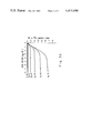
- FIGS. 3a and 3b depict the I-V (current-voltage) characteristics of n-channel and p-channel devices fabricated in accordance with the invention.
- FIG. 1a depicts a semiconductor substrate 10, preferably silicon, here lightly doped with n-type atoms, about 5 ⁇ 10 14 atoms/cm 3 , over which has been formed a dielectric layer 12.
- layer 12 is silicon dioxide, often referred to as the field oxide, and, in this process, is formed to a thickness of about 4,000 to 5,000 A. While the silicon substrate shown here is doped with n-type material, it should be understood that p-type silicon may alternatively be employed as a substrate for fabricating devices in accordance with the invention.
- NMOS and PMOS devices For fabricating NMOS and PMOS devices, a plurality of openings, one of which is shown at 14 (NMOS) and one of which is shown at 16 (PMOS), is formed in layer 12 by conventional masking and etching techniques to expose portions of the underlying substrate. These openings define the n-channel and p-channel regions, respectively, that will subsequently become the source, drain and channel regions of the NMOS and PMOS devices, respectively. As shown in FIG. 1b, a composite resist mask 18, called herein the "complementary" mask and described in greater detail below, is then formed over those openings which comprise the p-channel devices.
- P-type ions such as boron
- P-type ions are then implanted, shown at 20, to form simultaneously a p-well 22 a p + region (channel stop) 24 in the semiconductor substrate.
- the implantation is done under conditions such that the peak distribution of atoms lies in the silicon substrate just beneath the silicon/silicon dioxide interface 26 (i.e., within a few hundred A thereof) in order to overcome processing variations in oxide formation. This ensures that the p-doping concentration in the channel stop region 24 is maximum near the surface, while the p-doping concentration in p-well 22 is maximum at about half the depth of the p-well.
- the position of the distribution peak near the interface for the channel stop region serves to reduce parasitic conduction between neighboring transistors.
- N-type ions such as phosphorus
- the implantation energy is low enough such that the phosphorus atoms do not penetrate the field oxide.
- the channel stop region is therefore not affected by this phosphorus implant.
- This counter-doping process which is preferred because of the control over threshold voltage it provides, is more fully described in Ser. No. 142,902, filed Apr. 23, 1980 issued Feb. 16, 1982 as U.S. Pat. No. 4,315,781, and thus does not form a part of this invention.
- Simple experimentation is adequate for determining the particular conditions needed to establish the desired doping profile. For example, for a layer of silicon dioxide 4,000 A thick, a deep boron implant at a dosage of 1 ⁇ 10 13 /cm 2 at 120 keV and a shallow phosphorus implant at a dosage of 9 ⁇ 10 11 /cm 2 at 200 keV is sufficient to form the desired doping profiles in both the p-well and the channel stop regions. In the p-well region, the peak distribution of implanted atoms under these conditions is about 0.4 ⁇ m below the silicon surface.
- a metal layer 28 is then formed over the entire structure, such as by evaporation.
- the metal layer is thin enough to provide discontinuities between those regions covered with the composite resist and those regions not so covered, as shown in FIG. 1c.
- the photoresist composite should be at least twice as thick as the metal layer 28 in order to have metal discontinuity at the resist edges during lift-off of the metal.
- the required minimum thickness of the metal layer is an inverse function of its density. For example, an aluminum metal layer is formed to a thickness of about 5,000 A, while a gold metal layer is formed to a thickness of about 2,500 A. The purpose of this metal layer in ion implantation is discussed below.
- a single photoresist layer is required to be thicker than that customarily employed in the art. Ideally, a steep sidewall or even slight undercut is required in order to obtain the desired metal lift-off.
- the desired geometry is realized by employing a composite resist comprising two or more layers.
- a thick photoresist layer about 2 ⁇ m thick or a polysilicon (polycrystalline silicon) layer 18a about 1 ⁇ m thick is capped with a thin (about 0.5 to 1 ⁇ m) photoresist layer 18b.
- the thin photoresist layer provides the high resolution desired.
- the top resist layer is patterned and used as a mask, and the bottom layer is then over-developed (photoresist) or over-etched (polysilicon) slightly to obtain what is known in the art as the "mushroom" effect.
- photoresist photoresist
- polysilicon is employed as the bottom layer, since it is a better implant mask than photoresist.
- polysilicon does not dissolve during the lift-off process with the top photoresist layer, so it must be etched away, such as by a CF 4 plasma.
- a very thin oxide (not shown), about 200 A, is typically grown (prior to the polysilicon deposition) to serve as a plasma etch stop and to protect the silicon substrate surface. This thin oxide is then stripped and regrown subsequently to form a gate oxide, as described below.
- a three-layer resist structure (not shown) may be employed as the composite resist 18.
- a thick photoresist layer about 2 ⁇ m thick is formed on the substrate, followed by a thin metal layer, for example, about 1,000 A of aluminum, silicon or germanium, capped with a thin photoresist layer about 0.5 ⁇ m to 1 ⁇ m thick.
- the composite resist 18 is removed by dissolving the resist, thus taking with it (lifting off) the over-lying metal layer 28, leaving the structure shown in FIG. 1d.
- N-type ions such as phosphorus
- p-type ions are then implanted, shown at 30, to form simultaneously an n-well 32 and an n + region (channel stop) 34.
- the implantation is done under conditions such that the peak distribution of atoms lies in the substrate just beneath the substrate/field oxide interface 26.
- P-type ions, such as boron are then implanted into the n-well to counter-dope the surface region, as described above for the p-well formation.
- the metal mask 28 over the n-channel regions protects those regions against implantation.
- the metal selected and its thickness are such as to effectively stop the ion implantation, employing the considerations described above.
- both p-channel and n-channel stops are mutually self-aligned at 36. Self-alignment between adjacent n- and n-channel devices and p- and p-channel devices is also achieved.
- the substrate is then processed in accordance with prior art techniques for fabricating finished devices.
- gate oxides about 400 A thick are grown on the silicon substrate surface.
- Polysilicon gates (polysilicon highly doped to n + ) are formed thereover employing photoresist for masking.
- Sources and drains (n + ) for the n-channel devices and sources and drains (p + ) for the p-channel devices are implanted, employing conventional CMOS process technology.
- Appropriate contact holes are formed by conventional masking and etching, and the entire surface is metallized.
- the final electrode pattern is formed by conventional processes.
- FIG. 2 in cross-section, shows source 38 and drain 40 regions, with polysilicon gate 42 over region 22, forming an NMOS device. Electrode 46 contacts the source region, while electrode 48 contacts the drain region. Gate oxide 50 separates polysilicon gate 42 from the semiconductor surface. Likewise, in a PMOS device, gate oxide 52 separates polysilicon gate 54, which is positioned over region 32, from the semiconductor surface. Electrode 56 contacts source region 58 and electrode 60 contacts drain region 62.
- contacting schemes can, of course, be used.
- Exemplary of such contacting schemes is the refractory gate process, in which a refractory gate metal such as tungsten or molybdenum is employed.
- a refractory gate metal such as tungsten or molybdenum
- Other gate metals such as aluminum and metal silicide, may alternatively be employed.
- the process sequence of the invention thus comprises:
- the remaining steps to fabricate a completed device include:
- n + -regions for n-channel devices and heavily implant n-type (e.g., arsenic) ions for n-channel sources and drains by over-compensating previously implanted boron atoms (mask no. 4);
- n-type e.g., arsenic
- (j) define contact holes (mask no. 5) and form metallization pattern (mask no. 6).
- the central aspect of the invention depends on the success of the metal lift-off which is performed after the resist has been used as a mask during ion implantation.
- Metal lift-off can be a problem because it is difficult to maintain a resist profile suitable for the metal lift-off after ion implantation (e.g., 5,000 A of Al or 2,500 A of Au). Accordingly, the composite resist layer described above is employed to overcome this problem.
- a composite resist layer comprising 1 ⁇ m of polysilicon and 1 ⁇ m of Shipley AZ photoresist was deposited on a silicon substrate, employing 200 A of SiO 2 as a plasma etch stop. A single layer of 2 ⁇ m of AZ photoresist was also deposited on a silicon substrate. A 5,000 A layer of aluminum was deposited over each resist layer. The aluminum was successfully lifted off the composite resist, but not off the monolithic resist.
- the process disclosed herein provides a self-aligned n + channel stop between n- and n-channel devices and a self-aligned p + channel stop between p- and p-channel devices.
- the process also provides mutual self-alignment between these two channel stops.
- the process can be employed in submicrometer device fabrication.
- CMOS/SOS complementary metal-oxide-semiconductor
- n- and p-channel devices were fabricated, employing the procedures described above.
- the thickness of the field oxide 12 was 4,000 A, while that of the gate oxide 50, 52 was about 400 A.
- Boron was implanted deep to define p-wells 22 and p + channel stops 24 at a dosage of 1 ⁇ 10 13 /cm 2 at 120 keV.
- Phosphorus was then implanted shallow to counter-dope the p-well at a dosage of 9 ⁇ 10 11 /cm 2 at 200 keV in preparation for the formation of n-channel devices.
- Phosphorus was also implanted deep to define n-wells 32 and n + channel stops 34 at a dosage of 1.5 ⁇ 10 13 /cm 2 at 300 keV. Boron was then implanted shallow to counter-dope the n-well at a dosage of 7 ⁇ 10 12 /cm 2 at 50 keV in preparation for the formation of p-channel devices.
- the complementary mask comprised a 200 A SiO 2 plasma etch stop, a 1 ⁇ m thick polysilicon layer and a 1 ⁇ m thick Shipley AZ photoresist layer, over which was deposited 6,000 A of Al.
- the source 58 and drain 62 regions of the PMOS devices were formed by implanting boron at a dosage of 5 ⁇ 10 14 /cm 2 at 25 keV; the source 38 and drain 40 regions of the NMOS devices were likewise implanted at the same time. The source and drain regions of the NMOS devices were then implanted with arsenic at a dosage of 1.5 ⁇ 10 15 /cm 2 at 150 keV, to over-compensate for the previous p-doping.
- the gate contacts 42, 54 were polysilicon, diffused with phosphorus.
- the source and drain contacts 46, 48, 56, 60 comprised 4,000 A of a bilayer metal contact further comprised of a thin ohmic contact layer of WTi (90%:10% by wt.) underlying a relatively thicker conduction layer of aluminum.
- FIGS. 3a and 3b depicts the I-V characteristics of the 1 ⁇ m n- and p-channel MOSFET, respectively, at the gate voltages (V G ) given.
- Desirably high threshold voltages of 14 V and -32 V were also obtained for the n- and p-channel field transistors (parasitic transistors).
- CMOS/SOS devices using similar process parameters, including n-channel and p-channel MOSFETs, a series of CMOS/SOS inverters and a 31-stage CMOS/SOS ring oscillator, all on the same chip.
- MOSFETs and inverters functioned correctly.
Abstract
Description
Claims (27)
Priority Applications (4)
| Application Number | Priority Date | Filing Date | Title |
|---|---|---|---|
| US06/297,903 US4411058A (en) | 1981-08-31 | 1981-08-31 | Process for fabricating CMOS devices with self-aligned channel stops |
| DE8282304479T DE3278184D1 (en) | 1981-08-31 | 1982-08-25 | Cmos devices with self-aligned channel stops |
| EP82304479A EP0074215B1 (en) | 1981-08-31 | 1982-08-25 | Cmos devices with self-aligned channel stops |
| JP57150164A JPH0691201B2 (en) | 1981-08-31 | 1982-08-31 | Method for manufacturing CMOS semiconductor device |
Applications Claiming Priority (1)
| Application Number | Priority Date | Filing Date | Title |
|---|---|---|---|
| US06/297,903 US4411058A (en) | 1981-08-31 | 1981-08-31 | Process for fabricating CMOS devices with self-aligned channel stops |
Publications (1)
| Publication Number | Publication Date |
|---|---|
| US4411058A true US4411058A (en) | 1983-10-25 |
Family
ID=23148206
Family Applications (1)
| Application Number | Title | Priority Date | Filing Date |
|---|---|---|---|
| US06/297,903 Expired - Lifetime US4411058A (en) | 1981-08-31 | 1981-08-31 | Process for fabricating CMOS devices with self-aligned channel stops |
Country Status (4)
| Country | Link |
|---|---|
| US (1) | US4411058A (en) |
| EP (1) | EP0074215B1 (en) |
| JP (1) | JPH0691201B2 (en) |
| DE (1) | DE3278184D1 (en) |
Cited By (32)
| Publication number | Priority date | Publication date | Assignee | Title |
|---|---|---|---|---|
| US4471523A (en) * | 1983-05-02 | 1984-09-18 | International Business Machines Corporation | Self-aligned field implant for oxide-isolated CMOS FET |
| US4535532A (en) * | 1984-04-09 | 1985-08-20 | At&T Bell Laboratories | Integrated circuit contact technique |
| US4570331A (en) * | 1984-01-26 | 1986-02-18 | Inmos Corporation | Thick oxide field-shield CMOS process |
| US4578128A (en) * | 1984-12-03 | 1986-03-25 | Ncr Corporation | Process for forming retrograde dopant distributions utilizing simultaneous outdiffusion of dopants |
| US4578859A (en) * | 1984-08-22 | 1986-04-01 | Harris Corporation | Implant mask reversal process |
| US4584027A (en) * | 1984-11-07 | 1986-04-22 | Ncr Corporation | Twin well single mask CMOS process |
| US4599789A (en) * | 1984-06-15 | 1986-07-15 | Harris Corporation | Process of making twin well VLSI CMOS |
| US4600445A (en) * | 1984-09-14 | 1986-07-15 | International Business Machines Corporation | Process for making self aligned field isolation regions in a semiconductor substrate |
| US4604790A (en) * | 1985-04-01 | 1986-08-12 | Advanced Micro Devices, Inc. | Method of fabricating integrated circuit structure having CMOS and bipolar devices |
| WO1987005443A1 (en) * | 1986-03-04 | 1987-09-11 | Motorola, Inc. | High/low doping profile for twin well process |
| US4696092A (en) * | 1984-07-02 | 1987-09-29 | Texas Instruments Incorporated | Method of making field-plate isolated CMOS devices |
| US4707455A (en) * | 1986-11-26 | 1987-11-17 | General Electric Company | Method of fabricating a twin tub CMOS device |
| US4710477A (en) * | 1983-09-12 | 1987-12-01 | Hughes Aircraft Company | Method for forming latch-up immune, multiple retrograde well high density CMOS FET |
| US4889825A (en) * | 1986-03-04 | 1989-12-26 | Motorola, Inc. | High/low doping profile for twin well process |
| DE4114000A1 (en) * | 1990-05-02 | 1991-11-07 | Mitsubishi Electric Corp | Semiconductor device having substrate - with two well regions formed in surface of substrate independently |
| DE4101313A1 (en) * | 1990-10-05 | 1992-04-09 | Samsung Electronics Co Ltd | SEMICONDUCTOR COMPONENTS WITH A CHANNEL BARRIER AND METHOD FOR THE PRODUCTION THEREOF |
| US5292671A (en) * | 1987-10-08 | 1994-03-08 | Matsushita Electric Industrial, Co., Ltd. | Method of manufacture for semiconductor device by forming deep and shallow regions |
| US5384279A (en) * | 1988-09-09 | 1995-01-24 | U.S. Philips Corporation | Method of manufacturing a semiconductor device comprising a silicon body in which semiconductor regions are formed by ion implantations |
| US5459193A (en) * | 1993-10-12 | 1995-10-17 | H. B. Fuller Licensing & Financing, Inc. | Polystyrene-ethylene/butylene-polystyrene hot melt adhesive |
| US5863977A (en) * | 1993-10-12 | 1999-01-26 | H. B. Fuller Licensing & Financing, Inc. | High molecular weight S-EB-S hot melt adhesive |
| US5937284A (en) * | 1995-05-31 | 1999-08-10 | Mitsubishi Denki Kabushiki Kaisha | Method of making a semiconductor device having an SOI structure |
| US5956583A (en) * | 1997-06-30 | 1999-09-21 | Fuller; Robert T. | Method for forming complementary wells and self-aligned trench with a single mask |
| EP0996151A2 (en) * | 1998-10-20 | 2000-04-26 | Siemens Aktiengesellschaft | Method for fabricating transistors |
| US6093585A (en) * | 1998-05-08 | 2000-07-25 | Lsi Logic Corporation | High voltage tolerant thin film transistor |
| US6133077A (en) * | 1998-01-13 | 2000-10-17 | Lsi Logic Corporation | Formation of high-voltage and low-voltage devices on a semiconductor substrate |
| US6348736B1 (en) * | 1999-10-29 | 2002-02-19 | International Business Machines Corporation | In situ formation of protective layer on silsesquioxane dielectric for dual damascene process |
| US6764890B1 (en) * | 2003-01-29 | 2004-07-20 | Cypress Semiconductor Corporation | Method of adjusting the threshold voltage of a mosfet |
| US20040251497A1 (en) * | 2002-09-29 | 2004-12-16 | Advanced Analogic Technologies, Inc. | Modular bipolar-CMOS-DMOS analog integrated circuit and power transistor technology |
| US20040252250A1 (en) * | 2003-06-11 | 2004-12-16 | Lg.Philips Lcd Co., Ltd. | Liquid crystal display device and method of manufacturing the same |
| US20070278568A1 (en) * | 2006-05-31 | 2007-12-06 | Advanced Analogic Technologies, Inc. | High-voltage bipolar-CMOS-DMOS integrated circuit devices and modular methods of forming the same |
| US8497167B1 (en) * | 2007-01-17 | 2013-07-30 | National Semiconductor Corporation | EDS protection diode with pwell-nwell resurf |
| US9257504B2 (en) | 2002-09-29 | 2016-02-09 | Advanced Analogic Technologies Incorporated | Isolation structures for semiconductor devices |
Families Citing this family (6)
| Publication number | Priority date | Publication date | Assignee | Title |
|---|---|---|---|---|
| US4399605A (en) * | 1982-02-26 | 1983-08-23 | International Business Machines Corporation | Method of making dense complementary transistors |
| EP0164737B1 (en) * | 1984-06-15 | 1991-09-18 | Harris Corporation | A method of fabricating self-aligned regions in a substrate |
| US4558508A (en) * | 1984-10-15 | 1985-12-17 | International Business Machines Corporation | Process of making dual well CMOS semiconductor structure with aligned field-dopings using single masking step |
| JPS6197859A (en) * | 1984-10-18 | 1986-05-16 | Matsushita Electronics Corp | Manufacture of cmos ic |
| NL8501992A (en) * | 1985-07-11 | 1987-02-02 | Philips Nv | METHOD FOR MANUFACTURING A SEMICONDUCTOR DEVICE |
| US7087476B2 (en) * | 2004-07-28 | 2006-08-08 | Intel Corporation | Using different gate dielectrics with NMOS and PMOS transistors of a complementary metal oxide semiconductor integrated circuit |
Citations (11)
| Publication number | Priority date | Publication date | Assignee | Title |
|---|---|---|---|---|
| US3892609A (en) * | 1971-10-07 | 1975-07-01 | Hughes Aircraft Co | Production of mis integrated devices with high inversion voltage to threshold voltage ratios |
| US3983620A (en) * | 1975-05-08 | 1976-10-05 | National Semiconductor Corporation | Self-aligned CMOS process for bulk silicon and insulating substrate device |
| US4013484A (en) * | 1976-02-25 | 1977-03-22 | Intel Corporation | High density CMOS process |
| US4046606A (en) * | 1976-05-10 | 1977-09-06 | Rca Corporation | Simultaneous location of areas having different conductivities |
| US4110899A (en) * | 1976-01-12 | 1978-09-05 | Hitachi, Ltd. | Method for manufacturing complementary insulated gate field effect transistors |
| US4224733A (en) * | 1977-10-11 | 1980-09-30 | Fujitsu Limited | Ion implantation method |
| US4268321A (en) * | 1978-08-23 | 1981-05-19 | Hitachi, Ltd. | Method of fabricating a semiconductor device having channel stoppers |
| US4277291A (en) * | 1979-01-22 | 1981-07-07 | Sgs-Ates Componenti Elettronici S.P.A. | Process for making CMOS field-effect transistors |
| US4280272A (en) * | 1977-07-04 | 1981-07-28 | Tokyo Shibaura Denki Kabushiki Kaisha | Method for preparing complementary semiconductor device |
| US4306916A (en) * | 1979-09-20 | 1981-12-22 | American Microsystems, Inc. | CMOS P-Well selective implant method |
| US4315781A (en) * | 1980-04-23 | 1982-02-16 | Hughes Aircraft Company | Method of controlling MOSFET threshold voltage with self-aligned channel stop |
Family Cites Families (4)
| Publication number | Priority date | Publication date | Assignee | Title |
|---|---|---|---|---|
| JPS5270779A (en) * | 1975-12-09 | 1977-06-13 | Fujitsu Ltd | Manufacture of complementary-type integrated circuit |
| JPS52143782A (en) * | 1976-05-26 | 1977-11-30 | Hitachi Ltd | Construction of complementary mis-ic and its production |
| GB2024504B (en) * | 1978-06-29 | 1982-10-20 | Philips Electronic Associated | Manufacture of integrated circuits |
| JPS5691461A (en) * | 1979-12-25 | 1981-07-24 | Fujitsu Ltd | Manufacturing of complementary mos integrated circuit |
-
1981
- 1981-08-31 US US06/297,903 patent/US4411058A/en not_active Expired - Lifetime
-
1982
- 1982-08-25 DE DE8282304479T patent/DE3278184D1/en not_active Expired
- 1982-08-25 EP EP82304479A patent/EP0074215B1/en not_active Expired
- 1982-08-31 JP JP57150164A patent/JPH0691201B2/en not_active Expired - Lifetime
Patent Citations (11)
| Publication number | Priority date | Publication date | Assignee | Title |
|---|---|---|---|---|
| US3892609A (en) * | 1971-10-07 | 1975-07-01 | Hughes Aircraft Co | Production of mis integrated devices with high inversion voltage to threshold voltage ratios |
| US3983620A (en) * | 1975-05-08 | 1976-10-05 | National Semiconductor Corporation | Self-aligned CMOS process for bulk silicon and insulating substrate device |
| US4110899A (en) * | 1976-01-12 | 1978-09-05 | Hitachi, Ltd. | Method for manufacturing complementary insulated gate field effect transistors |
| US4013484A (en) * | 1976-02-25 | 1977-03-22 | Intel Corporation | High density CMOS process |
| US4046606A (en) * | 1976-05-10 | 1977-09-06 | Rca Corporation | Simultaneous location of areas having different conductivities |
| US4280272A (en) * | 1977-07-04 | 1981-07-28 | Tokyo Shibaura Denki Kabushiki Kaisha | Method for preparing complementary semiconductor device |
| US4224733A (en) * | 1977-10-11 | 1980-09-30 | Fujitsu Limited | Ion implantation method |
| US4268321A (en) * | 1978-08-23 | 1981-05-19 | Hitachi, Ltd. | Method of fabricating a semiconductor device having channel stoppers |
| US4277291A (en) * | 1979-01-22 | 1981-07-07 | Sgs-Ates Componenti Elettronici S.P.A. | Process for making CMOS field-effect transistors |
| US4306916A (en) * | 1979-09-20 | 1981-12-22 | American Microsystems, Inc. | CMOS P-Well selective implant method |
| US4315781A (en) * | 1980-04-23 | 1982-02-16 | Hughes Aircraft Company | Method of controlling MOSFET threshold voltage with self-aligned channel stop |
Cited By (75)
| Publication number | Priority date | Publication date | Assignee | Title |
|---|---|---|---|---|
| US4471523A (en) * | 1983-05-02 | 1984-09-18 | International Business Machines Corporation | Self-aligned field implant for oxide-isolated CMOS FET |
| US4710477A (en) * | 1983-09-12 | 1987-12-01 | Hughes Aircraft Company | Method for forming latch-up immune, multiple retrograde well high density CMOS FET |
| US4570331A (en) * | 1984-01-26 | 1986-02-18 | Inmos Corporation | Thick oxide field-shield CMOS process |
| US4535532A (en) * | 1984-04-09 | 1985-08-20 | At&T Bell Laboratories | Integrated circuit contact technique |
| US4599789A (en) * | 1984-06-15 | 1986-07-15 | Harris Corporation | Process of making twin well VLSI CMOS |
| US4696092A (en) * | 1984-07-02 | 1987-09-29 | Texas Instruments Incorporated | Method of making field-plate isolated CMOS devices |
| US4578859A (en) * | 1984-08-22 | 1986-04-01 | Harris Corporation | Implant mask reversal process |
| US4600445A (en) * | 1984-09-14 | 1986-07-15 | International Business Machines Corporation | Process for making self aligned field isolation regions in a semiconductor substrate |
| US4584027A (en) * | 1984-11-07 | 1986-04-22 | Ncr Corporation | Twin well single mask CMOS process |
| US4578128A (en) * | 1984-12-03 | 1986-03-25 | Ncr Corporation | Process for forming retrograde dopant distributions utilizing simultaneous outdiffusion of dopants |
| US4604790A (en) * | 1985-04-01 | 1986-08-12 | Advanced Micro Devices, Inc. | Method of fabricating integrated circuit structure having CMOS and bipolar devices |
| WO1987005443A1 (en) * | 1986-03-04 | 1987-09-11 | Motorola, Inc. | High/low doping profile for twin well process |
| US4889825A (en) * | 1986-03-04 | 1989-12-26 | Motorola, Inc. | High/low doping profile for twin well process |
| US4707455A (en) * | 1986-11-26 | 1987-11-17 | General Electric Company | Method of fabricating a twin tub CMOS device |
| US5292671A (en) * | 1987-10-08 | 1994-03-08 | Matsushita Electric Industrial, Co., Ltd. | Method of manufacture for semiconductor device by forming deep and shallow regions |
| US5384279A (en) * | 1988-09-09 | 1995-01-24 | U.S. Philips Corporation | Method of manufacturing a semiconductor device comprising a silicon body in which semiconductor regions are formed by ion implantations |
| DE4114000A1 (en) * | 1990-05-02 | 1991-11-07 | Mitsubishi Electric Corp | Semiconductor device having substrate - with two well regions formed in surface of substrate independently |
| US5428239A (en) * | 1990-05-02 | 1995-06-27 | Mitsubishi Denki Kabushiki Kaisha | Semiconductor device having retrograde well and diffusion-type well |
| DE4101313A1 (en) * | 1990-10-05 | 1992-04-09 | Samsung Electronics Co Ltd | SEMICONDUCTOR COMPONENTS WITH A CHANNEL BARRIER AND METHOD FOR THE PRODUCTION THEREOF |
| US5459193A (en) * | 1993-10-12 | 1995-10-17 | H. B. Fuller Licensing & Financing, Inc. | Polystyrene-ethylene/butylene-polystyrene hot melt adhesive |
| US5863977A (en) * | 1993-10-12 | 1999-01-26 | H. B. Fuller Licensing & Financing, Inc. | High molecular weight S-EB-S hot melt adhesive |
| US5937284A (en) * | 1995-05-31 | 1999-08-10 | Mitsubishi Denki Kabushiki Kaisha | Method of making a semiconductor device having an SOI structure |
| US5956583A (en) * | 1997-06-30 | 1999-09-21 | Fuller; Robert T. | Method for forming complementary wells and self-aligned trench with a single mask |
| US6133077A (en) * | 1998-01-13 | 2000-10-17 | Lsi Logic Corporation | Formation of high-voltage and low-voltage devices on a semiconductor substrate |
| US6194766B1 (en) | 1998-01-13 | 2001-02-27 | Lsi Logic Corporation | Integrated circuit having low voltage and high voltage devices on a common semiconductor substrate |
| US6093585A (en) * | 1998-05-08 | 2000-07-25 | Lsi Logic Corporation | High voltage tolerant thin film transistor |
| EP0996151A3 (en) * | 1998-10-20 | 2000-06-07 | Siemens Aktiengesellschaft | Method for fabricating transistors |
| EP0996151A2 (en) * | 1998-10-20 | 2000-04-26 | Siemens Aktiengesellschaft | Method for fabricating transistors |
| US6323103B1 (en) | 1998-10-20 | 2001-11-27 | Siemens Aktiengesellschaft | Method for fabricating transistors |
| CN1294646C (en) * | 1998-10-20 | 2007-01-10 | 西门子公司 | Method for producing transistor |
| US6348736B1 (en) * | 1999-10-29 | 2002-02-19 | International Business Machines Corporation | In situ formation of protective layer on silsesquioxane dielectric for dual damascene process |
| US7135738B2 (en) | 2002-09-29 | 2006-11-14 | Advanced Analogic Technologies, Inc. | Modular bipolar-CMOS-DMOS analog integrated circuit and power transistor technology |
| US9257504B2 (en) | 2002-09-29 | 2016-02-09 | Advanced Analogic Technologies Incorporated | Isolation structures for semiconductor devices |
| US20040259318A1 (en) * | 2002-09-29 | 2004-12-23 | Advanced Analogic Technologies, Inc. | Modular bipolar-CMOS-DMOS analog integrated circuit and power transistor technology |
| US20060157818A1 (en) * | 2002-09-29 | 2006-07-20 | Advanced Analogic Technologies, Inc. | Modular bipolar-CMOS-DMOS analog integrated circuit and power transistor technology |
| US20040251497A1 (en) * | 2002-09-29 | 2004-12-16 | Advanced Analogic Technologies, Inc. | Modular bipolar-CMOS-DMOS analog integrated circuit and power transistor technology |
| US7602023B2 (en) | 2002-09-29 | 2009-10-13 | Advanced Analogic Technologies, Inc. | Modular bipolar-CMOS-DMOS analog integrated circuit and power transistor technology |
| US7576391B2 (en) | 2002-09-29 | 2009-08-18 | Advanced Analogic Technologies, Inc. | High-voltage lateral trench MOSFET |
| US7202536B2 (en) | 2002-09-29 | 2007-04-10 | Advanced Analogic Technologies, Inc. | Modular bipolar-CMOS-DMOS analog integrated circuit and power transistor technology |
| US7211863B2 (en) * | 2002-09-29 | 2007-05-01 | Advanced Analogic Technologies, Inc. | Modular bipolar-CMOS-DMOS analog integrated circuit and power transistor technology |
| US7265434B2 (en) | 2002-09-29 | 2007-09-04 | Advanced Analogic Technologies, Inc. | Modular bipolar-CMOS-DMOS analog integrated circuit and power transistor technology |
| US7279399B2 (en) * | 2002-09-29 | 2007-10-09 | Advanced Analogic Technologies, Inc. | Method of forming isolated pocket in a semiconductor substrate |
| US20070272986A1 (en) * | 2002-09-29 | 2007-11-29 | Advanced Analogic Technologies, Inc. | Modular bipolar-CMOS-DMOS analog integrated circuit and power transistor technology |
| US10074716B2 (en) | 2002-09-29 | 2018-09-11 | Skyworks Solutions (Hong Kong) Limited | Saucer-shaped isolation structures for semiconductor devices |
| US20080023762A1 (en) * | 2002-09-29 | 2008-01-31 | Advanced Analogic Technologies, Inc. | Modular bipolar-CMOS-DMOS analog integrated circuit and power transistor technology |
| US9905640B2 (en) | 2002-09-29 | 2018-02-27 | Skyworks Solutions (Hong Kong) Limited | Isolation structures for semiconductor devices including trenches containing conductive material |
| US7602024B2 (en) | 2002-09-29 | 2009-10-13 | Advanced Analogic Technologies, Inc. | Modular bipolar-CMOS-DMOS analog integrated circuit and power transistor technology |
| US20080061377A1 (en) * | 2002-09-29 | 2008-03-13 | Advanced Analogic Technologies, Inc. | Modular bipolar-CMOS-DMOS analog integrated circuit and power transistor technology |
| US7745883B2 (en) | 2002-09-29 | 2010-06-29 | Advanced Analogic Technologies, Inc. | Modular bipolar-CMOS-DMOS analog integrated circuit and power transistor technology |
| US20080061376A1 (en) * | 2002-09-29 | 2008-03-13 | Advanced Analogic Technologies, Inc. | Modular bipolar-CMOS-DMOS analog integrated circuit & power transistor technology |
| US20080061375A1 (en) * | 2002-09-29 | 2008-03-13 | Advanced Analogic Technologies, Inc. | Modular bipolar-CMOS-DMOS analog integrated circuit and power transistor technology |
| US7608895B2 (en) | 2002-09-29 | 2009-10-27 | Advanced Analogic Technologies, Inc. | Modular CMOS analog integrated circuit and power technology |
| US7573105B2 (en) | 2002-09-29 | 2009-08-11 | Advanced Analogic Technologies, Inc. | Modular bipolar-CMOS-DMOS analog integrated circuit and power transistor technology |
| US20080067585A1 (en) * | 2002-09-29 | 2008-03-20 | Advanced Analogic Technologies, Inc. | High-voltage bipolar-CMOS-DMOS integrated circuit devices and modular methods of forming the same |
| US7605433B2 (en) | 2002-09-29 | 2009-10-20 | Advanced Analogic Technologies, Inc. | Modular bipolar-CMOS-DMOS analog integrated circuit and power transistor technology |
| US20080116513A1 (en) * | 2002-09-29 | 2008-05-22 | Advanced Analogic Technologies, Inc. | Modular bipolar-CMOS-DMOS analog integrated circuit and power transistor technology |
| WO2004030036A3 (en) * | 2002-09-29 | 2009-01-29 | Advanced Analogic Tech Inc | A modular bipolar-cmos-dmos analog integrated circuit and power transistor technology |
| US7605432B2 (en) | 2002-09-29 | 2009-10-20 | Advanced Analogic Technologies, Inc. | Modular bipolar-CMOS-DMOS analog integrated circuit and power transistor technology |
| US6764890B1 (en) * | 2003-01-29 | 2004-07-20 | Cypress Semiconductor Corporation | Method of adjusting the threshold voltage of a mosfet |
| US20040252250A1 (en) * | 2003-06-11 | 2004-12-16 | Lg.Philips Lcd Co., Ltd. | Liquid crystal display device and method of manufacturing the same |
| US7173675B2 (en) * | 2003-06-11 | 2007-02-06 | Lg. Philips Lcd Co., Ltd. | LCD display with contact hole and insulation layer above pixel electrode |
| US20080067586A1 (en) * | 2006-05-31 | 2008-03-20 | Advanced Analogic Technologies, Inc. | High-voltage bipolar-CMOS-DMOS integrated circuit devices and modular methods of forming the same |
| US7719054B2 (en) | 2006-05-31 | 2010-05-18 | Advanced Analogic Technologies, Inc. | High-voltage lateral DMOS device |
| US7489007B2 (en) | 2006-05-31 | 2009-02-10 | Advanced Analogic Technologies, Inc. | High-voltage lateral DMOS device |
| US20080067588A1 (en) * | 2006-05-31 | 2008-03-20 | Advanced Analogic Technologies, Inc. | High-voltage bipolar-CMOS-DMOS integrated circuit devices and modular methods of forming the same |
| US20080061400A1 (en) * | 2006-05-31 | 2008-03-13 | Advanced Analogic Technologies, Inc. | High-voltage bipolar-CMOS-DMOS integrated circuit devices and modular methods of forming the same |
| US7683426B2 (en) | 2006-05-31 | 2010-03-23 | Advanced Analogic Technologies, Inc. | High-voltage lateral DMOS device with diode clamp |
| US7683453B2 (en) | 2006-05-31 | 2010-03-23 | Advanced Analogic Technologies, Inc. | Edge termination region for high-voltage bipolar-CMOS-DMOS integrated circuit devices |
| US7605428B2 (en) | 2006-05-31 | 2009-10-20 | Advanced Analogic Technologies, Inc. | High-voltage depletion mode MOSFET |
| US20080061367A1 (en) * | 2006-05-31 | 2008-03-13 | Advanced Analogic Technologies, Inc. | High-voltage bipolar-CMOS-DMOS integrated circuit devices and modular methods of forming the same |
| US7812393B2 (en) | 2006-05-31 | 2010-10-12 | Advanced Analogic Technologies, Inc. | High-voltage extended drain MOSFET |
| US20070278568A1 (en) * | 2006-05-31 | 2007-12-06 | Advanced Analogic Technologies, Inc. | High-voltage bipolar-CMOS-DMOS integrated circuit devices and modular methods of forming the same |
| US20080061368A1 (en) * | 2006-05-31 | 2008-03-13 | Advanced Analogic Technologies, Inc. | High-voltage bipolar-CMOS-DMOS integrated circuit devices and modular methods of forming the same |
| WO2007142937A3 (en) * | 2006-05-31 | 2008-03-06 | Advanced Analogic Tech Inc | High-voltage bipolar-cmos-dmos integrated circuit devices and modular methods of forming the same |
| US8497167B1 (en) * | 2007-01-17 | 2013-07-30 | National Semiconductor Corporation | EDS protection diode with pwell-nwell resurf |
Also Published As
| Publication number | Publication date |
|---|---|
| EP0074215A2 (en) | 1983-03-16 |
| EP0074215A3 (en) | 1984-12-27 |
| JPS5878453A (en) | 1983-05-12 |
| EP0074215B1 (en) | 1988-03-02 |
| JPH0691201B2 (en) | 1994-11-14 |
| DE3278184D1 (en) | 1988-04-07 |
Similar Documents
| Publication | Publication Date | Title |
|---|---|---|
| US4411058A (en) | Process for fabricating CMOS devices with self-aligned channel stops | |
| US6312997B1 (en) | Low voltage high performance semiconductor devices and methods | |
| US4946799A (en) | Process for making high performance silicon-on-insulator transistor with body node to source node connection | |
| US4899202A (en) | High performance silicon-on-insulator transistor with body node to source node connection | |
| US4752589A (en) | Process for the production of bipolar transistors and complementary MOS transistors on a common silicon substrate | |
| US4306916A (en) | CMOS P-Well selective implant method | |
| US4965213A (en) | Silicon-on-insulator transistor with body node to source node connection | |
| US5371024A (en) | Semiconductor device and process for manufacturing the same | |
| US4013484A (en) | High density CMOS process | |
| US5294822A (en) | Polycide local interconnect method and structure | |
| US4135955A (en) | Process for fabricating high voltage cmos with self-aligned guard rings utilizing selective diffusion and local oxidation | |
| US4536947A (en) | CMOS process for fabricating integrated circuits, particularly dynamic memory cells with storage capacitors | |
| US4849364A (en) | Semiconductor devices | |
| EP0139019A1 (en) | Semiconductor device and method of manufacture thereof | |
| US4505026A (en) | CMOS Process for fabricating integrated circuits, particularly dynamic memory cells | |
| US4229756A (en) | Ultra high speed complementary MOS device | |
| US4488348A (en) | Method for making a self-aligned vertically stacked gate MOS device | |
| US4114256A (en) | Reliable metal-to-junction contacts in large-scale-integrated devices | |
| US4471523A (en) | Self-aligned field implant for oxide-isolated CMOS FET | |
| KR970003898B1 (en) | Method of manufacturing a semiconductor integrated circuit device | |
| US4223334A (en) | High voltage CMOS with local oxidation for self-aligned guard rings and process of fabrication | |
| US5612243A (en) | Polycide local interconnect method and structure | |
| US6071781A (en) | Method of fabricating lateral MOS transistor | |
| KR930005508B1 (en) | Semiconductor device and manufacturing method of the same | |
| US6218253B1 (en) | Method of manufacturing a bipolar transistor by using only two mask layers |
Legal Events
| Date | Code | Title | Description |
|---|---|---|---|
| AS | Assignment |
Owner name: HUGHES AIRCRAFT COMPANY CULVER CITY, CA. A CORP. Free format text: ASSIGNMENT OF ASSIGNORS INTEREST.;ASSIGNOR:CHEN, JOHN Y.;REEL/FRAME:003916/0930 Effective date: 19810825 |
|
| STCF | Information on status: patent grant |
Free format text: PATENTED CASE |
|
| MAFP | Maintenance fee payment |
Free format text: PAYMENT OF MAINTENANCE FEE, 4TH YEAR, PL 96-517 (ORIGINAL EVENT CODE: M170); ENTITY STATUS OF PATENT OWNER: LARGE ENTITY Year of fee payment: 4 |
|
| FEPP | Fee payment procedure |
Free format text: MAINTENANCE FEE REMINDER MAILED (ORIGINAL EVENT CODE: REM.); ENTITY STATUS OF PATENT OWNER: LARGE ENTITY |
|
| FEPP | Fee payment procedure |
Free format text: SURCHARGE FOR LATE PAYMENT, PL 96-517 (ORIGINAL EVENT CODE: M176); ENTITY STATUS OF PATENT OWNER: LARGE ENTITY |
|
| MAFP | Maintenance fee payment |
Free format text: PAYMENT OF MAINTENANCE FEE, 8TH YEAR, PL 96-517 (ORIGINAL EVENT CODE: M171); ENTITY STATUS OF PATENT OWNER: LARGE ENTITY Year of fee payment: 8 |
|
| FEPP | Fee payment procedure |
Free format text: PAYOR NUMBER ASSIGNED (ORIGINAL EVENT CODE: ASPN); ENTITY STATUS OF PATENT OWNER: LARGE ENTITY |
|
| AS | Assignment |
Owner name: HUGHES ELECTRONICS CORPORATION, CALIFORNIA Free format text: ASSIGNMENT OF ASSIGNORS INTEREST;ASSIGNOR:HE HOLDINGS INC., HUGHES ELECTRONICS FORMERLY KNOWN AS HUGHES AIRCRAFT COMPANY;REEL/FRAME:009350/0366 Effective date: 19971217 |