US4412277A - AC-DC Converter having an improved power factor - Google Patents
AC-DC Converter having an improved power factor Download PDFInfo
- Publication number
- US4412277A US4412277A US06/414,757 US41475782A US4412277A US 4412277 A US4412277 A US 4412277A US 41475782 A US41475782 A US 41475782A US 4412277 A US4412277 A US 4412277A
- Authority
- US
- United States
- Prior art keywords
- signal
- generating
- current
- reference signal
- control
- Prior art date
- Legal status (The legal status is an assumption and is not a legal conclusion. Google has not performed a legal analysis and makes no representation as to the accuracy of the status listed.)
- Expired - Lifetime
Links
Images

Classifications
-
- H—ELECTRICITY
- H02—GENERATION; CONVERSION OR DISTRIBUTION OF ELECTRIC POWER
- H02M—APPARATUS FOR CONVERSION BETWEEN AC AND AC, BETWEEN AC AND DC, OR BETWEEN DC AND DC, AND FOR USE WITH MAINS OR SIMILAR POWER SUPPLY SYSTEMS; CONVERSION OF DC OR AC INPUT POWER INTO SURGE OUTPUT POWER; CONTROL OR REGULATION THEREOF
- H02M1/00—Details of apparatus for conversion
- H02M1/42—Circuits or arrangements for compensating for or adjusting power factor in converters or inverters
- H02M1/4208—Arrangements for improving power factor of AC input
-
- H—ELECTRICITY
- H02—GENERATION; CONVERSION OR DISTRIBUTION OF ELECTRIC POWER
- H02M—APPARATUS FOR CONVERSION BETWEEN AC AND AC, BETWEEN AC AND DC, OR BETWEEN DC AND DC, AND FOR USE WITH MAINS OR SIMILAR POWER SUPPLY SYSTEMS; CONVERSION OF DC OR AC INPUT POWER INTO SURGE OUTPUT POWER; CONTROL OR REGULATION THEREOF
- H02M1/00—Details of apparatus for conversion
- H02M1/0083—Converters characterised by their input or output configuration
- H02M1/0085—Partially controlled bridges
-
- H—ELECTRICITY
- H02—GENERATION; CONVERSION OR DISTRIBUTION OF ELECTRIC POWER
- H02M—APPARATUS FOR CONVERSION BETWEEN AC AND AC, BETWEEN AC AND DC, OR BETWEEN DC AND DC, AND FOR USE WITH MAINS OR SIMILAR POWER SUPPLY SYSTEMS; CONVERSION OF DC OR AC INPUT POWER INTO SURGE OUTPUT POWER; CONTROL OR REGULATION THEREOF
- H02M7/00—Conversion of ac power input into dc power output; Conversion of dc power input into ac power output
- H02M7/02—Conversion of ac power input into dc power output without possibility of reversal
- H02M7/04—Conversion of ac power input into dc power output without possibility of reversal by static converters
- H02M7/12—Conversion of ac power input into dc power output without possibility of reversal by static converters using discharge tubes with control electrode or semiconductor devices with control electrode
- H02M7/21—Conversion of ac power input into dc power output without possibility of reversal by static converters using discharge tubes with control electrode or semiconductor devices with control electrode using devices of a triode or transistor type requiring continuous application of a control signal
- H02M7/217—Conversion of ac power input into dc power output without possibility of reversal by static converters using discharge tubes with control electrode or semiconductor devices with control electrode using devices of a triode or transistor type requiring continuous application of a control signal using semiconductor devices only
- H02M7/2173—Conversion of ac power input into dc power output without possibility of reversal by static converters using discharge tubes with control electrode or semiconductor devices with control electrode using devices of a triode or transistor type requiring continuous application of a control signal using semiconductor devices only in a biphase or polyphase circuit arrangement
-
- H—ELECTRICITY
- H02—GENERATION; CONVERSION OR DISTRIBUTION OF ELECTRIC POWER
- H02M—APPARATUS FOR CONVERSION BETWEEN AC AND AC, BETWEEN AC AND DC, OR BETWEEN DC AND DC, AND FOR USE WITH MAINS OR SIMILAR POWER SUPPLY SYSTEMS; CONVERSION OF DC OR AC INPUT POWER INTO SURGE OUTPUT POWER; CONTROL OR REGULATION THEREOF
- H02M1/00—Details of apparatus for conversion
- H02M1/42—Circuits or arrangements for compensating for or adjusting power factor in converters or inverters
- H02M1/4208—Arrangements for improving power factor of AC input
- H02M1/4233—Arrangements for improving power factor of AC input using a bridge converter comprising active switches
-
- Y—GENERAL TAGGING OF NEW TECHNOLOGICAL DEVELOPMENTS; GENERAL TAGGING OF CROSS-SECTIONAL TECHNOLOGIES SPANNING OVER SEVERAL SECTIONS OF THE IPC; TECHNICAL SUBJECTS COVERED BY FORMER USPC CROSS-REFERENCE ART COLLECTIONS [XRACs] AND DIGESTS
- Y02—TECHNOLOGIES OR APPLICATIONS FOR MITIGATION OR ADAPTATION AGAINST CLIMATE CHANGE
- Y02B—CLIMATE CHANGE MITIGATION TECHNOLOGIES RELATED TO BUILDINGS, e.g. HOUSING, HOUSE APPLIANCES OR RELATED END-USER APPLICATIONS
- Y02B70/00—Technologies for an efficient end-user side electric power management and consumption
- Y02B70/10—Technologies improving the efficiency by using switched-mode power supplies [SMPS], i.e. efficient power electronics conversion e.g. power factor correction or reduction of losses in power supplies or efficient standby modes
-
- Y—GENERAL TAGGING OF NEW TECHNOLOGICAL DEVELOPMENTS; GENERAL TAGGING OF CROSS-SECTIONAL TECHNOLOGIES SPANNING OVER SEVERAL SECTIONS OF THE IPC; TECHNICAL SUBJECTS COVERED BY FORMER USPC CROSS-REFERENCE ART COLLECTIONS [XRACs] AND DIGESTS
- Y02—TECHNOLOGIES OR APPLICATIONS FOR MITIGATION OR ADAPTATION AGAINST CLIMATE CHANGE
- Y02P—CLIMATE CHANGE MITIGATION TECHNOLOGIES IN THE PRODUCTION OR PROCESSING OF GOODS
- Y02P80/00—Climate change mitigation technologies for sector-wide applications
- Y02P80/10—Efficient use of energy, e.g. using compressed air or pressurized fluid as energy carrier
Definitions
- This invention relates to AC-DC converters and in particular to AC-DC converters that provide a unity power factor to sinusoidal AC sources.
- AC-DC power converters There are essentially two types of prior art AC-DC power converters; those that have a capacitor type input filter and those that have an choke type input filter.
- the AC to DC converters that have a capacitor type input filter have associated therewith peak charging currents for charging the capacitors that are located within the capacitor type input filter.
- the choke type input filters have squarewave currents which are detrimental to the power line that drives the AC to DC converter. In both cases, the conventional AC to DC converters produce input line currents that have undesirable harmonic contents that, if removed, must be done so by large power filters.
- An AC to DC converter utilizes a first power converter for converting an AC signal to a DC signal under the control of a control signal.
- the control signal is generated by a control circuit that includes a first analog generator that provides a first signal that is analogous to the voltage of the AC signal that is to be converted.
- a second analog generator generates a second signal that is analogous to the current of the AC signal that is to be converted and a third analog generator generates a third signal that is analogous to the voltage of the DC output signal.
- the third signal and the first signal are multiplied together to obtain a fourth signal.
- the control signal is generated from the fourth signal and the second signal and is used to control the power converter such that the waveform of the current of the AC signal is limited to a sinusoidal waveform of the same frequency and phase as the AC signal.
- the control signal is generated by the comparison of the fourth signal with the second signal to obtain a difference signal.
- the difference signal is then compared with a high frequency sawtooth waveform and is used to generate the control signal that is used to drive the AC to DC converter.
- the AC to DC converter is a full wave AC to DC converter that is capable of being controlled by the control signal. This is accomplished by replacing any two diodes in adjacent legs of a conventional bridge configuration with FET switches which respond to the control signals.
- the selected FET switches that are used have associated therewith an intrinsic diodes which enables the bridge to be configured by two diodes and two FET switches.
- the FET switches will cycle on and off with a duty factor that varies in accordance with the control signal in order to achieve the same waveform for the current of the AC signal as the voltage waveform of the AC signal.
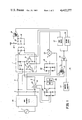
- FIG. 1 is a schematic diagram of the AC to DC converter according to the invention.
- FIG. 2 is a waveform diagram that illustrates the operation of the AC to DC converter of FIG. 1.
- FIG. 1 there is shown an AC to DC converter 10 according to the invention.
- An AC signal source 1 provides an AC signal via high frequency filter 35 across terminals 3 and 5 which is represented as a voltage V 1 .
- the voltage V 1 is applied to a full wave rectifier 7 via chokes 9 and 11.
- the full wave rectifier 7 is a bridge configuration with two diodes 13 and 15 in two adjacent legs and two power MOSFET switches 17 and 19 in the other two adjacent legs.
- an intrinsic diode 21 represented by dash lines in the embodiment of FIG. 1.
- the embodiment of the converter illustrated in FIG. 1 has the advantage that it is not necessary to steer the power MOSFET's gate signals because the intrinsic diodes contact naturally when they are forward biased.
- the gating of the power MOSFETs 17 and 19 is performed at a frequency much higher than the frequency of the voltage V 1 with a duty factor that is varied in accordance with the control signal that is applied to the gates of the power MOSFETS switches 17 and 19 to insure the sinusoidal waveform of the input current I 1 which is represented by arrow 23.
- Duty factor is defined as the ratio of the time the power MOSFET's switches 17 and 19 are gated on in each period of the total time of each period.
- the output of the power converter 7 is applied across an output capacitor 25 across to which the output DC voltage V 2 is provided and applied to a load 27.
- a full wave bridge rectifier 29 rectifies the voltage V 1 that is applied to the AC to DC converter and obtains an analog signal that is analogous to the voltage V 1 .
- the V 1 analog signal is divided down by a resistor divider network 31 and applied to a multiplier 33.
- the V 1 analog signal is represented in FIG. 1 by the vector Y 1 .
- An error amplifier 35 compares the output signal V 2 with a reference signal that is provided by a potentiometer 37 and a DC reference source (not shown).
- Resistor divider network 39 and 41 divide V 2 proportionally down for comparison with the reference signal that is provided from the wiper of potentiometer 37 to the error amplifier 35 and a signal Y 3 that is analogous to the output signal V 2 is obtained and applied to the multiplier 33 where it is multiplied with the analog signal Y 1 to form a current reference signal, Y 4 .
- Y 3 by action of the multiplier 33 varies the amplitude of Y 1 to obtain Y 4 .
- the sensed signal is applied to a full wave rectifier 45 where an analogous voltage is developed across the output of the full wave rectifier 45 by a resistor 47.
- the high frequency ripple component of the voltage is filtered by a filter 49 and applied to a second error amplifier 51.
- the analog signal of the current provided by the AC source 1 is denoted Y 2 and is compared by an error amplifier 51 to Y 4 to obtain Y 5 which is the amplified difference between the two signals.
- Y 5 is then compared by a comparator 53 with a sawtooth waveform provided by the sawtooth generator 55 that results in a pulse being provided on the output of the comparator 53 for the period of time that the output signal from the sawtooth generator is greater than Y 5 .
- a first driver 57 and a second driver 59 provide gating signals to the power MOSFETs 17 and 19 respectively.
- the error amplifier 35 varies the sinusoidal amplitude of I 1 as necessary to keep the output voltage at V 2 level regardless of the input voltage V 1 or load and must be true for all switching rates of the power MOSFETs 17 and 19.
- the second error amplifier 51 tries to achieve a zero error between the signals Y 4 and Y 2 by varying the duty factor of the power MOSFETs 17 and 19 and assures that the wave shape of current I 1 is the same as the voltage V 1 .
- the sawtooth generator provides a sawtooth waveform that has a frequency that is much higher than the input frequency provided by the AC source 1.
- the frequency of the sawtooth generator 55 is 40 KHz. This high frequency is removed from the AC to DC convertor's 10 circuits by the high frequency filters 35 and 49.
- FIG. 2 During a positive half cycle of the AC signal V 1 , represented in FIG. 2 by waveform 135, current I 1 passes through the line chokes 9 and 11, intrinsic diode 21 of power MOSFET 19 and alternately at a high frequency rate through diode 13 and power MOSFET 17 depending upon the state of the gate signal from the first driver 57.
- the gate signal is represented by waveform 153 of FIG. 2.
- I 1 builds up through line chokes 9 and 11; when power MOSFET 17 is off, the energy stored in the line chokes 9 and 11 is transferred to the output capacitor 25 via diode 13.
- the waveform for I 1 prior to being filtered by the high frequency filter 35 is represented by the waveform 137 and after filtering by the high frequency filter 35 the waveform for I 1 is represented by waveform 123 of FIG. 2.
- power MOSFET 19 and diode 15 are activated during a negative half cycle of the AC signal V 1 .
- the power MOSFET 19 duty factor is determined by the comparison of the output signal Y 5 and the high frequency sawtooth reference signal from the sawtooth generator 55. This comparison is graphically illustrated by waveforms 151 and 153 of FIG. 2 where waveform 155 is the output of the sawtooth generator 55. The waveform 155 of FIG. 2 is at a much slower rate than the preferred embodiment of 40 kHz. This is for illustration purposes only so that the invention may be more clearly understood. Additionally, V 1 is illustrated as a sinusoidal waveform as is the waveform for I 1 however any waveform that is a function of time may be substituted for V 1 and consequently I 1 will follow that waveform due to the control of the conduction of the power MOSFETs 17 and 19. In the embodiment of FIG.
- the conduction of the power MOSFET 19 is controlled in such a manner that the envelope of the resulting high frequency sawtooth waveform 137 of I 1 is sinusoidal flowing from terminal 3 and is in phase with V 1 .
- the line chokes 9 and 11 are designed so that the peak to peak sawtooth amplitude of I 1 is about one tenth the peak line frequency value in order to minimize the size of the high frequency input filter 35.
- the high frequency operation of either power MOSFET 17 and diode 13 insures that the steady state value of V 2 is equal to or greater than the peak value of V 1 .
Abstract
Description
Claims (8)
Priority Applications (1)
| Application Number | Priority Date | Filing Date | Title |
|---|---|---|---|
| US06/414,757 US4412277A (en) | 1982-09-03 | 1982-09-03 | AC-DC Converter having an improved power factor |
Applications Claiming Priority (1)
| Application Number | Priority Date | Filing Date | Title |
|---|---|---|---|
| US06/414,757 US4412277A (en) | 1982-09-03 | 1982-09-03 | AC-DC Converter having an improved power factor |
Publications (1)
| Publication Number | Publication Date |
|---|---|
| US4412277A true US4412277A (en) | 1983-10-25 |
Family
ID=23642826
Family Applications (1)
| Application Number | Title | Priority Date | Filing Date |
|---|---|---|---|
| US06/414,757 Expired - Lifetime US4412277A (en) | 1982-09-03 | 1982-09-03 | AC-DC Converter having an improved power factor |
Country Status (1)
| Country | Link |
|---|---|
| US (1) | US4412277A (en) |
Cited By (74)
| Publication number | Priority date | Publication date | Assignee | Title |
|---|---|---|---|---|
| US4499533A (en) * | 1982-09-14 | 1985-02-12 | Matsushita Electric Works, Ltd. | Power supply apparatus |
| WO1987004023A1 (en) * | 1985-12-23 | 1987-07-02 | Sundstrand Corporation | Emi reduction circuit |
| EP0307719A2 (en) * | 1987-09-16 | 1989-03-22 | Hitachi, Ltd. | Power source apparatus |
| US4853837A (en) * | 1988-08-08 | 1989-08-01 | Zdzislaw Gulczynski | Synchronous switching power supply with flyback converter |
| US4855890A (en) * | 1987-06-24 | 1989-08-08 | Reliance Comm/Tec Corporation | Power factor correction circuit |
| US4866585A (en) * | 1988-06-08 | 1989-09-12 | Das Pawan K | AC to DC solid state power supply using high frequency pulsed power switching |
| US4914559A (en) * | 1988-01-19 | 1990-04-03 | American Telephone And Telegraph Company | Power factor improving arrangement |
| US4924372A (en) * | 1989-07-26 | 1990-05-08 | Westinghouse Electric Corp. | Single phase rectifier circuit |
| US4933831A (en) * | 1988-09-19 | 1990-06-12 | Isao Takahashi | Power supply |
| US4940929A (en) * | 1989-06-23 | 1990-07-10 | Apollo Computer, Inc. | AC to DC converter with unity power factor |
| US4956600A (en) * | 1988-07-01 | 1990-09-11 | Viteq Corporation | High frequency current detector for a low frequency line |
| US4964029A (en) * | 1988-05-18 | 1990-10-16 | Viteq Corporation | AC to DC power converter with input current waveform control for buck-boost regulation of output |
| US4980812A (en) * | 1989-11-09 | 1990-12-25 | Exide Electronics | Uninterrupted power supply system having improved power factor correction circuit |
| US5019952A (en) * | 1989-11-20 | 1991-05-28 | General Electric Company | AC to DC power conversion circuit with low harmonic distortion |
| EP0442286A2 (en) * | 1990-02-14 | 1991-08-21 | Usi Lighting, Inc. | Power factor correction circuit |
| US5121316A (en) * | 1991-05-13 | 1992-06-09 | Modular Devices, Inc. | Electronic system and method for correcting the power factor of an accessory to a main equipment |
| EP0504094A2 (en) * | 1991-03-15 | 1992-09-16 | Emerson Electric Co. | High power factor converter for motor drives and power supplies |
| EP0507663A1 (en) * | 1991-04-05 | 1992-10-07 | Artus | Method and apparatus for attenuating the effect of conducted radiointerference on the polyphase AC network |
| EP0516122A2 (en) * | 1991-05-31 | 1992-12-02 | Kabushiki Kaisha Toshiba | Inverter power supply |
| US5289361A (en) * | 1991-01-16 | 1994-02-22 | Vlt Corporation | Adaptive boost switching preregulator and method |
| US5301095A (en) * | 1991-10-01 | 1994-04-05 | Origin Electric Company, Limited | High power factor AC/DC converter |
| EP0593257A2 (en) * | 1992-10-12 | 1994-04-20 | Nemic-Lambda Kabushiki Kaisha | Boost converter |
| US5359276A (en) * | 1993-05-12 | 1994-10-25 | Unitrode Corporation | Automatic gain selection for high power factor |
| EP0637789A1 (en) * | 1993-07-28 | 1995-02-08 | AT&T Corp. | Power factor control arrangement for an ols based on quarter cycle averaged power flow |
| US5399955A (en) * | 1990-09-27 | 1995-03-21 | At&T Corp. | Power factor improving arrangement |
| US5446366A (en) * | 1994-02-08 | 1995-08-29 | Computer Products, Inc. | Boost converter power supply with reduced losses, control circuit and method therefor |
| US5450029A (en) * | 1993-06-25 | 1995-09-12 | At&T Corp. | Circuit for estimating a peak or RMS value of a sinusoidal voltage waveform |
| EP0778993A1 (en) * | 1994-08-30 | 1997-06-18 | SOOHOO, Ronald, F. | Miniaturized high frequency direct current power supply |
| US5719493A (en) * | 1995-08-31 | 1998-02-17 | Minolta Co., Ltd. | Electrical device |
| US5751561A (en) * | 1995-10-16 | 1998-05-12 | Computer Products, Inc. | Low cost AC-to-DC converter having input current with reduced harmonics |
| US5774350A (en) * | 1995-04-07 | 1998-06-30 | Sgs-Thomson Microelectronics S.A. | Integrated low dissipation power controller |
| US5995383A (en) * | 1995-10-16 | 1999-11-30 | Computer Products, Inc. | Low cost AC-to-DC converter having input current with reduced harmonics |
| US6038146A (en) * | 1997-06-13 | 2000-03-14 | Computer Products, Incorporated | High power factors, single stage harmonics correction converter |
| US6084786A (en) * | 1999-01-29 | 2000-07-04 | Hamilton Sundstrand Corporation | Converter system with power factor and DC ripple control |
| US6178101B1 (en) * | 1997-08-15 | 2001-01-23 | Unitron, Inc. | Power supply regulation |
| WO2002089303A1 (en) * | 2001-04-26 | 2002-11-07 | Powerlab A/S | Ac-dc converter with no input rectifying diode bridge |
| US6653822B2 (en) * | 2001-02-22 | 2003-11-25 | Koninklijke Philips Electronics N.V. | Circuit for converting AC voltage into DC voltage |
| US20050083715A1 (en) * | 2002-01-22 | 2005-04-21 | Nicolas Guillarme | Multicellular dc/dc voltage converter with protection switches |
| US20050105311A1 (en) * | 2003-10-01 | 2005-05-19 | International Rectifier Corporation | Bridge-less boost (BLB) power factor correction topology controlled with one cycle control |
| EP1564618A1 (en) * | 2004-02-14 | 2005-08-17 | Jungheinrich Aktiengesellschaft | Circuit for power factor correction in switching power supplies, chargers and the like |
| EP1575152A2 (en) * | 2004-03-12 | 2005-09-14 | Comarco Wireless Technologies, Inc. | Power factor correction circuits |
| US20060198172A1 (en) * | 2003-10-01 | 2006-09-07 | International Rectifier Corporation | Bridgeless boost converter with PFC circuit |
| US20060208711A1 (en) * | 2004-12-14 | 2006-09-21 | International Rectifier Corp. | EMI noise reduction circuit and method for bridgeless PFC circuit |
| US20060220628A1 (en) * | 2005-03-31 | 2006-10-05 | International Rectifier Corporation | Current sense method for bridgeless boost (BLB) PFC circuit using single current transformer |
| US20070171690A1 (en) * | 2006-01-26 | 2007-07-26 | Silicon Laboratories, Inc. | Active diode bridge system and method |
| US20070170903A1 (en) * | 2006-01-26 | 2007-07-26 | Silicon Laboratories, Inc. | Active diode bridge system |
| WO2008044120A2 (en) * | 2006-10-11 | 2008-04-17 | O.C.E.M. S.P.A. | A device for supplying power to led diodes |
| WO2009070031A1 (en) | 2007-11-29 | 2009-06-04 | Eltek Valere As | Control system and method for controlling a bridgeless boost converter |
| US20100046259A1 (en) * | 2008-08-20 | 2010-02-25 | ConvenientPower HK Ltd. | Single-phase self-driven full-bridge synchrounous rectification |
| US20100046264A1 (en) * | 2008-08-20 | 2010-02-25 | ConvenientPower HK Ltd. | Generalized ac-dc synchronous rectification techniques for single- and multi-phase systems |
| WO2010110802A1 (en) * | 2009-03-27 | 2010-09-30 | Hewlett-Packard Development Company, L.P. | Rectifier circuit with reduced power dissipation |
| US20110235380A1 (en) * | 2010-03-23 | 2011-09-29 | Qualcomm Incorporated | Power conversion |
| WO2011131012A1 (en) * | 2010-04-22 | 2011-10-27 | 华为技术有限公司 | Power factor correction converter and power supply and control method thereof |
| US8385032B1 (en) | 2011-08-23 | 2013-02-26 | Futurewei Technologies, Inc. | High efficiency bridgeless PFC converter and method |
| WO2013188119A1 (en) * | 2012-06-13 | 2013-12-19 | Efficient Power Conversion Corporation | Method for operating a non-isolated switching converter having synchronous rectification capability suitable for power factor correction applications |
| KR101357070B1 (en) | 2006-06-30 | 2014-02-04 | 페어차일드 세미컨덕터 코포레이션 | High-efficiency power converter system |
| KR101381940B1 (en) * | 2011-10-31 | 2014-04-18 | 단국대학교 산학협력단 | Rectifier and input controling method of the same |
| US20150062987A1 (en) * | 2013-08-29 | 2015-03-05 | Silergy Semiconductor Technology (Hangzhou) Ltd | Load driving circuit and method thereof |
| EP2882083A1 (en) | 2013-12-05 | 2015-06-10 | ABB Technology AG | Bridgeless power factor correction circuit |
| TWI492500B (en) * | 2013-04-19 | 2015-07-11 | Silergy Corp | AC / DC converter control circuit and the application of its AC / DC converter |
| DE102014106578A1 (en) | 2014-05-09 | 2015-11-12 | Minebea Co., Ltd. | CIRCUIT WITH POWER FACTOR CORRECTION FILTER AND RECTIFIER OR INVERTER |
| US9270166B2 (en) | 2012-12-20 | 2016-02-23 | Tdk Corporation | Power factor improvement circuit |
| US9490694B2 (en) | 2014-03-14 | 2016-11-08 | Delta-Q Technologies Corp. | Hybrid resonant bridgeless AC-DC power factor correction converter |
| US9590495B2 (en) | 2011-08-26 | 2017-03-07 | Futurewei Technologies, Inc. | Holdup time circuit and method for bridgeless PFC converter |
| USD796431S1 (en) | 2015-06-12 | 2017-09-05 | Delta-Q Technologies Corp. | Battery charger |
| USD806647S1 (en) | 2015-08-11 | 2018-01-02 | Delta-Q Technologies Corp. | Battery charger |
| USD815592S1 (en) | 2016-05-18 | 2018-04-17 | Delta-Q Technologies Corp. | Battery charger |
| USD854497S1 (en) | 2016-12-05 | 2019-07-23 | Delta-Q Technologies Corp. | Battery charger |
| US10720787B2 (en) | 2017-07-26 | 2020-07-21 | Delta-Q Technologies Corp. | Combined charger and power converter |
| US10879813B2 (en) | 2018-09-21 | 2020-12-29 | Delta-Q Technologies Corp. | Bridgeless single-stage AC/DC converter |
| IT202000014323A1 (en) | 2020-06-16 | 2021-12-16 | Eggtronic Eng S P A | APPARATUS FOR TRANSFERING ELECTRIC POWER TO AN ELECTRIC LOAD WITH CONVERTER |
| US11355962B2 (en) | 2018-09-26 | 2022-06-07 | Eggtronic Engineering S.P.A. | Apparatus for transferring electrical power to an electrical load with converter |
| USD1004541S1 (en) | 2020-05-05 | 2023-11-14 | Delta-Q Technologies Corp. | Battery charger |
| USD1022880S1 (en) | 2021-11-29 | 2024-04-16 | Delta-Q Technologies Corp. | Battery charger |
Citations (5)
| Publication number | Priority date | Publication date | Assignee | Title |
|---|---|---|---|---|
| US3238383A (en) * | 1963-05-31 | 1966-03-01 | Barnes Eng Co | Ripple-free synchronous demodulator circuit |
| US3896287A (en) * | 1973-07-11 | 1975-07-22 | Air Prod & Chem | Direct current arc power supply |
| US4074345A (en) * | 1976-11-02 | 1978-02-14 | Ackermann Walter J | Electronic power supply |
| US4150325A (en) * | 1977-12-02 | 1979-04-17 | General Electric Company | Power conversion system having inversion fault detection and correction circuit |
| US4245293A (en) * | 1977-10-08 | 1981-01-13 | Hitachi, Ltd. | Power converter system |
-
1982
- 1982-09-03 US US06/414,757 patent/US4412277A/en not_active Expired - Lifetime
Patent Citations (5)
| Publication number | Priority date | Publication date | Assignee | Title |
|---|---|---|---|---|
| US3238383A (en) * | 1963-05-31 | 1966-03-01 | Barnes Eng Co | Ripple-free synchronous demodulator circuit |
| US3896287A (en) * | 1973-07-11 | 1975-07-22 | Air Prod & Chem | Direct current arc power supply |
| US4074345A (en) * | 1976-11-02 | 1978-02-14 | Ackermann Walter J | Electronic power supply |
| US4245293A (en) * | 1977-10-08 | 1981-01-13 | Hitachi, Ltd. | Power converter system |
| US4150325A (en) * | 1977-12-02 | 1979-04-17 | General Electric Company | Power conversion system having inversion fault detection and correction circuit |
Cited By (115)
| Publication number | Priority date | Publication date | Assignee | Title |
|---|---|---|---|---|
| US4499533A (en) * | 1982-09-14 | 1985-02-12 | Matsushita Electric Works, Ltd. | Power supply apparatus |
| WO1987004023A1 (en) * | 1985-12-23 | 1987-07-02 | Sundstrand Corporation | Emi reduction circuit |
| US4730243A (en) * | 1985-12-23 | 1988-03-08 | Sundstrand Corporation | EMI reduction circuit |
| US4855890A (en) * | 1987-06-24 | 1989-08-08 | Reliance Comm/Tec Corporation | Power factor correction circuit |
| EP0307719A3 (en) * | 1987-09-16 | 1989-08-30 | Hitachi, Ltd. | Power source apparatus |
| US5050057A (en) * | 1987-09-16 | 1991-09-17 | Hitachi, Ltd. | Power source apparatus |
| EP0307719A2 (en) * | 1987-09-16 | 1989-03-22 | Hitachi, Ltd. | Power source apparatus |
| US4914559A (en) * | 1988-01-19 | 1990-04-03 | American Telephone And Telegraph Company | Power factor improving arrangement |
| US4964029A (en) * | 1988-05-18 | 1990-10-16 | Viteq Corporation | AC to DC power converter with input current waveform control for buck-boost regulation of output |
| US4866585A (en) * | 1988-06-08 | 1989-09-12 | Das Pawan K | AC to DC solid state power supply using high frequency pulsed power switching |
| US4956600A (en) * | 1988-07-01 | 1990-09-11 | Viteq Corporation | High frequency current detector for a low frequency line |
| US4853837A (en) * | 1988-08-08 | 1989-08-01 | Zdzislaw Gulczynski | Synchronous switching power supply with flyback converter |
| US4933831A (en) * | 1988-09-19 | 1990-06-12 | Isao Takahashi | Power supply |
| US4940929A (en) * | 1989-06-23 | 1990-07-10 | Apollo Computer, Inc. | AC to DC converter with unity power factor |
| US4924372A (en) * | 1989-07-26 | 1990-05-08 | Westinghouse Electric Corp. | Single phase rectifier circuit |
| US4980812A (en) * | 1989-11-09 | 1990-12-25 | Exide Electronics | Uninterrupted power supply system having improved power factor correction circuit |
| WO1991007808A1 (en) * | 1989-11-09 | 1991-05-30 | Exide Electronics International Corporation | An uninterrupted power supply system having improved power factor correction circuit |
| US5019952A (en) * | 1989-11-20 | 1991-05-28 | General Electric Company | AC to DC power conversion circuit with low harmonic distortion |
| EP0442286A2 (en) * | 1990-02-14 | 1991-08-21 | Usi Lighting, Inc. | Power factor correction circuit |
| EP0442286A3 (en) * | 1990-02-14 | 1992-04-08 | Usi Lighting, Inc. | Power factor correction circuit |
| US5399955A (en) * | 1990-09-27 | 1995-03-21 | At&T Corp. | Power factor improving arrangement |
| US5289361A (en) * | 1991-01-16 | 1994-02-22 | Vlt Corporation | Adaptive boost switching preregulator and method |
| EP0504094A3 (en) * | 1991-03-15 | 1992-11-25 | Emerson Electric Co. | High power factor converter for motor drives and power supplies |
| EP0504094A2 (en) * | 1991-03-15 | 1992-09-16 | Emerson Electric Co. | High power factor converter for motor drives and power supplies |
| EP0507663A1 (en) * | 1991-04-05 | 1992-10-07 | Artus | Method and apparatus for attenuating the effect of conducted radiointerference on the polyphase AC network |
| FR2675000A1 (en) * | 1991-04-05 | 1992-10-09 | Artus | METHOD AND DEVICE FOR MITIGATING THE EFFECT OF CONDUCTIVE RADIOPARASITATION ON THE ALTERNATIVE POLYPHASE NETWORK. |
| US5121316A (en) * | 1991-05-13 | 1992-06-09 | Modular Devices, Inc. | Electronic system and method for correcting the power factor of an accessory to a main equipment |
| EP0516122A2 (en) * | 1991-05-31 | 1992-12-02 | Kabushiki Kaisha Toshiba | Inverter power supply |
| EP0516122A3 (en) * | 1991-05-31 | 1993-01-27 | Kabushiki Kaisha Toshiba | Inverter power supply |
| US5301095A (en) * | 1991-10-01 | 1994-04-05 | Origin Electric Company, Limited | High power factor AC/DC converter |
| EP0593257A3 (en) * | 1992-10-12 | 1995-02-01 | Nemic Lambda Kk | Boost converter. |
| EP0593257A2 (en) * | 1992-10-12 | 1994-04-20 | Nemic-Lambda Kabushiki Kaisha | Boost converter |
| US5359276A (en) * | 1993-05-12 | 1994-10-25 | Unitrode Corporation | Automatic gain selection for high power factor |
| US5450029A (en) * | 1993-06-25 | 1995-09-12 | At&T Corp. | Circuit for estimating a peak or RMS value of a sinusoidal voltage waveform |
| EP0637789A1 (en) * | 1993-07-28 | 1995-02-08 | AT&T Corp. | Power factor control arrangement for an ols based on quarter cycle averaged power flow |
| US5391976A (en) * | 1993-07-28 | 1995-02-21 | At&T Corp. | Power factor control arrangement for an OLS based on quarter cycle averaged power flow |
| US5446366A (en) * | 1994-02-08 | 1995-08-29 | Computer Products, Inc. | Boost converter power supply with reduced losses, control circuit and method therefor |
| EP0778993A1 (en) * | 1994-08-30 | 1997-06-18 | SOOHOO, Ronald, F. | Miniaturized high frequency direct current power supply |
| EP0778993A4 (en) * | 1994-08-30 | 1999-12-15 | Ronald F Soohoo | Miniaturized high frequency direct current power supply |
| US5774350A (en) * | 1995-04-07 | 1998-06-30 | Sgs-Thomson Microelectronics S.A. | Integrated low dissipation power controller |
| US5719493A (en) * | 1995-08-31 | 1998-02-17 | Minolta Co., Ltd. | Electrical device |
| US5751561A (en) * | 1995-10-16 | 1998-05-12 | Computer Products, Inc. | Low cost AC-to-DC converter having input current with reduced harmonics |
| US5995383A (en) * | 1995-10-16 | 1999-11-30 | Computer Products, Inc. | Low cost AC-to-DC converter having input current with reduced harmonics |
| US6038146A (en) * | 1997-06-13 | 2000-03-14 | Computer Products, Incorporated | High power factors, single stage harmonics correction converter |
| US6178101B1 (en) * | 1997-08-15 | 2001-01-23 | Unitron, Inc. | Power supply regulation |
| US6084786A (en) * | 1999-01-29 | 2000-07-04 | Hamilton Sundstrand Corporation | Converter system with power factor and DC ripple control |
| US6653822B2 (en) * | 2001-02-22 | 2003-11-25 | Koninklijke Philips Electronics N.V. | Circuit for converting AC voltage into DC voltage |
| WO2002089303A1 (en) * | 2001-04-26 | 2002-11-07 | Powerlab A/S | Ac-dc converter with no input rectifying diode bridge |
| US20050083715A1 (en) * | 2002-01-22 | 2005-04-21 | Nicolas Guillarme | Multicellular dc/dc voltage converter with protection switches |
| US7405495B2 (en) * | 2002-01-22 | 2008-07-29 | Johnson Controls Automotive Electronics | Multicellular DC/DC voltage converter with protection switches |
| US7164591B2 (en) | 2003-10-01 | 2007-01-16 | International Rectifier Corporation | Bridge-less boost (BLB) power factor correction topology controlled with one cycle control |
| US20060198172A1 (en) * | 2003-10-01 | 2006-09-07 | International Rectifier Corporation | Bridgeless boost converter with PFC circuit |
| US20050105311A1 (en) * | 2003-10-01 | 2005-05-19 | International Rectifier Corporation | Bridge-less boost (BLB) power factor correction topology controlled with one cycle control |
| EP1564618A1 (en) * | 2004-02-14 | 2005-08-17 | Jungheinrich Aktiengesellschaft | Circuit for power factor correction in switching power supplies, chargers and the like |
| EP1575152A2 (en) * | 2004-03-12 | 2005-09-14 | Comarco Wireless Technologies, Inc. | Power factor correction circuits |
| US20050201124A1 (en) * | 2004-03-12 | 2005-09-15 | Comarco Wireless Technologies, Inc. | Power factor correction circuits |
| EP1575152A3 (en) * | 2004-03-12 | 2006-03-08 | Comarco Wireless Technologies, Inc. | Power factor correction circuits |
| US7489116B2 (en) | 2004-03-12 | 2009-02-10 | Comarco Wireless Technologies, Inc. | Power factor correction control circuit |
| US20070296380A1 (en) * | 2004-03-12 | 2007-12-27 | Comarco Wireless Technologies, Inc. | Power factor correction control circuit |
| US7420823B2 (en) | 2004-03-12 | 2008-09-02 | Comarco Wireless Technologies, Inc | Power factor correction control circuit |
| US20080019154A1 (en) * | 2004-03-12 | 2008-01-24 | Comarco Wireless Technologies, Inc. | Power factor correction control circuit |
| US7279868B2 (en) | 2004-03-12 | 2007-10-09 | Comarco Wireless Technologies, Inc. | Power factor correction circuits |
| US20060208711A1 (en) * | 2004-12-14 | 2006-09-21 | International Rectifier Corp. | EMI noise reduction circuit and method for bridgeless PFC circuit |
| US7215560B2 (en) | 2004-12-14 | 2007-05-08 | International Rectifier Corporation | EMI noise reduction circuit and method for bridgeless PFC circuit |
| US7355868B2 (en) | 2005-03-31 | 2008-04-08 | International Rectifier Corporation | Current sense method for bridgeless boost (BLB) PFC circuit using single current transformer |
| US20060220628A1 (en) * | 2005-03-31 | 2006-10-05 | International Rectifier Corporation | Current sense method for bridgeless boost (BLB) PFC circuit using single current transformer |
| US20070171690A1 (en) * | 2006-01-26 | 2007-07-26 | Silicon Laboratories, Inc. | Active diode bridge system and method |
| US20070170903A1 (en) * | 2006-01-26 | 2007-07-26 | Silicon Laboratories, Inc. | Active diode bridge system |
| KR101357070B1 (en) | 2006-06-30 | 2014-02-04 | 페어차일드 세미컨덕터 코포레이션 | High-efficiency power converter system |
| US20100102737A1 (en) * | 2006-10-11 | 2010-04-29 | O.C.E.M. S.P.A. | Device For Supplying Power To LED Diodes |
| WO2008044120A2 (en) * | 2006-10-11 | 2008-04-17 | O.C.E.M. S.P.A. | A device for supplying power to led diodes |
| WO2008044120A3 (en) * | 2006-10-11 | 2008-06-12 | Ocem Spa | A device for supplying power to led diodes |
| US8072154B2 (en) | 2006-10-11 | 2011-12-06 | O.C.E.M. S.P.A. | Device for supplying power to LED diodes |
| WO2009070031A1 (en) | 2007-11-29 | 2009-06-04 | Eltek Valere As | Control system and method for controlling a bridgeless boost converter |
| US20100046264A1 (en) * | 2008-08-20 | 2010-02-25 | ConvenientPower HK Ltd. | Generalized ac-dc synchronous rectification techniques for single- and multi-phase systems |
| US20100046259A1 (en) * | 2008-08-20 | 2010-02-25 | ConvenientPower HK Ltd. | Single-phase self-driven full-bridge synchrounous rectification |
| US8942018B2 (en) | 2008-08-20 | 2015-01-27 | ConvenientPower HK Ltd. | Single-phase self-driven full-bridge synchronous rectification |
| US8711593B2 (en) | 2008-08-20 | 2014-04-29 | ConvenientPower HK Ltd. | Generalized AC-DC synchronous rectification techniques for single- and multi-phase systems |
| WO2010110802A1 (en) * | 2009-03-27 | 2010-09-30 | Hewlett-Packard Development Company, L.P. | Rectifier circuit with reduced power dissipation |
| US8750007B2 (en) * | 2010-03-23 | 2014-06-10 | Qualcomm Incorporated | Power conversion |
| US20110235380A1 (en) * | 2010-03-23 | 2011-09-29 | Qualcomm Incorporated | Power conversion |
| WO2011131012A1 (en) * | 2010-04-22 | 2011-10-27 | 华为技术有限公司 | Power factor correction converter and power supply and control method thereof |
| US8432138B2 (en) | 2010-04-22 | 2013-04-30 | Huawei Technologies Co., Ltd. | Power factor correction converter and control method thereof |
| US8385032B1 (en) | 2011-08-23 | 2013-02-26 | Futurewei Technologies, Inc. | High efficiency bridgeless PFC converter and method |
| US10411591B2 (en) | 2011-08-26 | 2019-09-10 | Futurewei Technologies, Inc. | Holdup time circuit and method for bridgeless PFC converter |
| US9590495B2 (en) | 2011-08-26 | 2017-03-07 | Futurewei Technologies, Inc. | Holdup time circuit and method for bridgeless PFC converter |
| KR101381940B1 (en) * | 2011-10-31 | 2014-04-18 | 단국대학교 산학협력단 | Rectifier and input controling method of the same |
| WO2013188119A1 (en) * | 2012-06-13 | 2013-12-19 | Efficient Power Conversion Corporation | Method for operating a non-isolated switching converter having synchronous rectification capability suitable for power factor correction applications |
| US9634555B2 (en) | 2012-06-13 | 2017-04-25 | Efficient Power Conversion Corporation | Method for operating a non-isolated switching converter having synchronous rectification capability suitable for power factor correction applications |
| TWI489751B (en) * | 2012-06-13 | 2015-06-21 | Efficient Power Conversion Corp | Power factor correction boost circuit and synchronous rectifier |
| US9270166B2 (en) | 2012-12-20 | 2016-02-23 | Tdk Corporation | Power factor improvement circuit |
| TWI492500B (en) * | 2013-04-19 | 2015-07-11 | Silergy Corp | AC / DC converter control circuit and the application of its AC / DC converter |
| US9627992B2 (en) | 2013-04-19 | 2017-04-18 | Silergy Semiconductor Technology (Hangzhou) Ltd | Controlling circuit and AC/DC converter thereof |
| US20150062987A1 (en) * | 2013-08-29 | 2015-03-05 | Silergy Semiconductor Technology (Hangzhou) Ltd | Load driving circuit and method thereof |
| US9190931B2 (en) * | 2013-08-29 | 2015-11-17 | Silergy Semiconductor Technology (Hangzhou) Ltd | Load driving circuit and method thereof |
| US9621068B2 (en) * | 2013-08-29 | 2017-04-11 | Silergy Semiconductor Technology (Hangzhou) Ltd | Load driving circuit and method thereof |
| US20160036345A1 (en) * | 2013-08-29 | 2016-02-04 | Silergy Semiconductor Technology (Hangzhou) Ltd | Load driving circuit and method thereof |
| EP2882083A1 (en) | 2013-12-05 | 2015-06-10 | ABB Technology AG | Bridgeless power factor correction circuit |
| US9093917B2 (en) | 2013-12-05 | 2015-07-28 | Abb Technology Ag | Bridgeless power factor correction circuit |
| US9490694B2 (en) | 2014-03-14 | 2016-11-08 | Delta-Q Technologies Corp. | Hybrid resonant bridgeless AC-DC power factor correction converter |
| DE102014106578A1 (en) | 2014-05-09 | 2015-11-12 | Minebea Co., Ltd. | CIRCUIT WITH POWER FACTOR CORRECTION FILTER AND RECTIFIER OR INVERTER |
| USD796431S1 (en) | 2015-06-12 | 2017-09-05 | Delta-Q Technologies Corp. | Battery charger |
| USD828294S1 (en) | 2015-06-12 | 2018-09-11 | Delta-Q Technologies Corp. | Battery charger |
| USD806647S1 (en) | 2015-08-11 | 2018-01-02 | Delta-Q Technologies Corp. | Battery charger |
| USD829649S1 (en) | 2015-08-11 | 2018-10-02 | Delta-Q Technologies Corp. | Battery charger |
| USD853956S1 (en) | 2016-05-18 | 2019-07-16 | Delta-Q Technologies Corp. | Battery charger |
| USD815592S1 (en) | 2016-05-18 | 2018-04-17 | Delta-Q Technologies Corp. | Battery charger |
| USD854497S1 (en) | 2016-12-05 | 2019-07-23 | Delta-Q Technologies Corp. | Battery charger |
| USD884612S1 (en) | 2016-12-05 | 2020-05-19 | Delta-Q Technologies Corp. | Battery charger |
| US10720787B2 (en) | 2017-07-26 | 2020-07-21 | Delta-Q Technologies Corp. | Combined charger and power converter |
| US10879813B2 (en) | 2018-09-21 | 2020-12-29 | Delta-Q Technologies Corp. | Bridgeless single-stage AC/DC converter |
| US11355962B2 (en) | 2018-09-26 | 2022-06-07 | Eggtronic Engineering S.P.A. | Apparatus for transferring electrical power to an electrical load with converter |
| USD1004541S1 (en) | 2020-05-05 | 2023-11-14 | Delta-Q Technologies Corp. | Battery charger |
| IT202000014323A1 (en) | 2020-06-16 | 2021-12-16 | Eggtronic Eng S P A | APPARATUS FOR TRANSFERING ELECTRIC POWER TO AN ELECTRIC LOAD WITH CONVERTER |
| USD1022880S1 (en) | 2021-11-29 | 2024-04-16 | Delta-Q Technologies Corp. | Battery charger |
Similar Documents
| Publication | Publication Date | Title |
|---|---|---|
| US4412277A (en) | AC-DC Converter having an improved power factor | |
| US4943902A (en) | AC to DC power converter and method with integrated line current control for improving power factor | |
| US4816982A (en) | AC to DC power converter with integrated line current control for improving power factor | |
| US4017784A (en) | DC to DC converter | |
| EP0500789B1 (en) | An uninterrupted power supply system having improved power factor correction circuit | |
| US4354223A (en) | Step-up/step down chopper | |
| US4823249A (en) | High-frequency resonant power converter | |
| US3913002A (en) | Power circuits for obtaining a high power factor electronically | |
| JPH0851790A (en) | Control circuit for inductive load | |
| US4074344A (en) | High power factor ac to dc converter circuit | |
| JPS5649693A (en) | Frequency converter | |
| JPH036718U (en) | ||
| US4158881A (en) | DC to DC converter | |
| US4253139A (en) | Power conversion and regulation system | |
| JPH07131984A (en) | Dc power supply equipment | |
| US5652699A (en) | High-voltage and high-power stabilized DC power supply using modified sine wave output 3-phase inverter | |
| JP4275223B2 (en) | Power supply | |
| JPH0720371B2 (en) | DC power supply | |
| JPH02168864A (en) | Dc power supply device | |
| JPS61244275A (en) | Pwm control voltage type inverter | |
| JPS63314176A (en) | Variable voltage/variable frequency power apparatus | |
| JP2550325B2 (en) | Power supply | |
| JPS56166765A (en) | Rectified power source system | |
| JP3263962B2 (en) | DC braking system | |
| JP3253349B2 (en) | Pulse width modulation circuit of laser power supply |
Legal Events
| Date | Code | Title | Description |
|---|---|---|---|
| AS | Assignment |
Owner name: ROCKWELL INTERNATIONAL CORPORATION Free format text: ASSIGNMENT OF ASSIGNORS INTEREST.;ASSIGNOR:MITCHELL, DANIEL M.;REEL/FRAME:004089/0140 Effective date: 19820827 |
|
| STCF | Information on status: patent grant |
Free format text: PATENTED CASE |
|
| MAFP | Maintenance fee payment |
Free format text: PAYMENT OF MAINTENANCE FEE, 4TH YEAR, PL 97-247 (ORIGINAL EVENT CODE: M173); ENTITY STATUS OF PATENT OWNER: LARGE ENTITY Year of fee payment: 4 |
|
| FEPP | Fee payment procedure |
Free format text: PAYOR NUMBER ASSIGNED (ORIGINAL EVENT CODE: ASPN); ENTITY STATUS OF PATENT OWNER: LARGE ENTITY |
|
| MAFP | Maintenance fee payment |
Free format text: PAYMENT OF MAINTENANCE FEE, 8TH YEAR, PL 97-247 (ORIGINAL EVENT CODE: M174); ENTITY STATUS OF PATENT OWNER: LARGE ENTITY Year of fee payment: 8 |
|
| FEPP | Fee payment procedure |
Free format text: MAINTENANCE FEE REMINDER MAILED (ORIGINAL EVENT CODE: REM.); ENTITY STATUS OF PATENT OWNER: LARGE ENTITY |
|
| FEPP | Fee payment procedure |
Free format text: SURCHARGE FOR LATE PAYMENT, LARGE ENTITY (ORIGINAL EVENT CODE: M186); ENTITY STATUS OF PATENT OWNER: LARGE ENTITY |
|
| MAFP | Maintenance fee payment |
Free format text: PAYMENT OF MAINTENANCE FEE, 12TH YEAR, LARGE ENTITY (ORIGINAL EVENT CODE: M185); ENTITY STATUS OF PATENT OWNER: LARGE ENTITY Year of fee payment: 12 |