US4425645A - Digital data transmission with parity bit word lock-on - Google Patents
Digital data transmission with parity bit word lock-on Download PDFInfo
- Publication number
- US4425645A US4425645A US06/311,783 US31178381A US4425645A US 4425645 A US4425645 A US 4425645A US 31178381 A US31178381 A US 31178381A US 4425645 A US4425645 A US 4425645A
- Authority
- US
- United States
- Prior art keywords
- parity
- bit
- bits
- bit stream
- serial
- Prior art date
- Legal status (The legal status is an assumption and is not a legal conclusion. Google has not performed a legal analysis and makes no representation as to the accuracy of the status listed.)
- Expired - Fee Related
Links
Images


Classifications
-
- H—ELECTRICITY
- H04—ELECTRIC COMMUNICATION TECHNIQUE
- H04L—TRANSMISSION OF DIGITAL INFORMATION, e.g. TELEGRAPHIC COMMUNICATION
- H04L1/00—Arrangements for detecting or preventing errors in the information received
- H04L1/004—Arrangements for detecting or preventing errors in the information received by using forward error control
- H04L1/0056—Systems characterized by the type of code used
- H04L1/0057—Block codes
-
- H—ELECTRICITY
- H04—ELECTRIC COMMUNICATION TECHNIQUE
- H04L—TRANSMISSION OF DIGITAL INFORMATION, e.g. TELEGRAPHIC COMMUNICATION
- H04L7/00—Arrangements for synchronising receiver with transmitter
- H04L7/04—Speed or phase control by synchronisation signals
- H04L7/048—Speed or phase control by synchronisation signals using the properties of error detecting or error correcting codes, e.g. parity as synchronisation signal
Definitions
- Asynchronous transmission involves sending equal length bursts of data, with a common data character format for this purpose comprising a start bit, the data bits (with or without a parity bit) and one or more stop bits. No clock information is sent with the data since the receiver easily resynchronizes at the beginning of each character. A large percentage of overhead bits are required for asynchronous transmission.
- Synchronous transmission involves sending blocks of data bits together with synchronizing, or framing, characters at, say, one hundred byte intervals of data. With synchronous transmission, much lower percentage of overhead bits are required. Now, however, the data must include therein the synchronizing, or framing, characters. Also, much more complex error checking schemes are required for synchronous systems compared to asynchronous systems if the loss of large blocks of information is to be avoided when transmission errors occur and synchronization is lost. With the present invention, the only overhead bits required are word parity bits which often are transmitted in any case.
- An object of this invention is the provision of improved method and means for transferring data in the form of a bit stream consisting of words comprising data bits and a parity bit without the need for synchronizing or framing characters, start and stop bits, or the like.
- An object of this invention is the provision of parity bit word lock-on method and means for generating word clock pulses in response to a bit stream of the above-mentioned type synchronized with word parity bits included in the stream.
- a parity bit to digital data bits to provide a serial bit stream consisting of equal length words each of which comprises a plurality of data bits and a parity bit.
- the signal is encoded and the encoded signal is transferred to a receiving location without accompanying word synchronization, clock, or timing signals.
- a "self-clocking" type code is employed for encoding the signal, which allows for the generation of bit clock pulses during decoding.
- bit clock pulses are generated and the signal is decoded returning the same to its original form i.e. a bit stream consisting of equal length words each of which consists of a plurality of data bits and a parity bit.
- the decoded output then is employed to generate word clock pulses synchronized with the parity bits.
- a method of locking onto the parity bit of the bit stream is employed which includes parity checking word length groups of bits every bit interval to produce parity true and parity error signals when parity is correct and incorrect, respectively. All parity true signals and the first occurring parity error signals for each integral multiple word length group of bits (i.e. data bits plus the parity bit) are stored in memory means which is at least one word length in size.
- the stored parity signals are examined and a word clock pulse is generated in synchronization with the parity bit of the stream when only one parity true signal is stored in one word length portion of said memory means. When said portion of memory contains only parity error signals and no parity true signal, it is reloaded with all parity true signals and generation of word clock pulses is terminated until parity bit lock-on again is achieved.
- FIG. 1 is a simplified block diagram showing a digital data transmission system embodying the present invention
- FIG. 2 includes a graphic representation showing the format of data from the parity bit generator included in FIG. 1 together with bit and word clock pulses for the data;
- FIG. 3A and 3B together show a block diagram of a digital transmission and receiving system which embodies the present invention; a transmitter unit being shown in FIG. 3A and a receiving unit being shown in FIG. 3B;
- FIG. 4 is a block diagram of a novel parity bit lock-on circuit embodying the present invention and which may be employed in the systems shown in FIG. 1 and FIGS. 3A and 3B; and
- FIG. 5 shows signals appearing at various locations of the parity bit lock-on circuit shown in FIG. 4 for use in explaining operation thereof.
- FIG. 1 wherein a system for transmitting and receiving a serial bit stream is shown in which the transmitter unit comprises a parity bit generator 10 and the receiver unit comprises a parity bit lock-on circuit 12, with the transmitter and receiving units being interconnected by a transmission line 14.
- Either serial or parallel digital data bits to be transmitted are supplied to the parity bit generator 10, together with word clock pulses from any desired suitable source thereof, not shown.
- word clock pulses from any desired suitable source thereof, not shown.
- Bit clock pulses are available at a second output line 18T of the generator for clocking the data and parity bits from the generator.
- the parity bit generator outputs at lines 16T and 18T thereof are depicted in FIG. 2, to which reference also is made.
- the nth word together with portions of the (n-1)st and (n+1)st words at line 16T of the generator are shown, and identified by reference character 20.
- Each word of the serial bit stream comprises a plurality of data bits, here ten, together with a parity bit.
- word is used to identify data bits plus the associated parity bit.
- a stream of eleven (11) bit words is shown, each of which words consists of a plurality of data bits (here, ten), and a parity bit.
- the parity bit proceeds the data bits in the stream.
- Bit clock pulses 22 are shown synchronized with the stream bits.
- the serial bit stream is transmitted to the receiver unit by any suitable means, including the illustrated transmission line 14.
- the stream may be encoded, and the encoded signal transferred to a receiver having a decoder to return the signal to its original form.
- bit clock pulses are shown supplied to the receiver over line 18R.
- a code of the "self-bit-clocking" type may be employed to avoid the need to actually transmit the bit clock.
- self-bit-clocking codes bit clock signals are generated by the decoder from the transmitted data bit stream without a bit clock pulse input to the decoder. Such an arrangement is shown in FIG. 3A and 3B, described below.
- bit clock pulses are actually transmitted, or are generated at the receiver, the original serial bit stream is reproduced at the receiver and supplied as an input to the parity lock-on circuit 12 thereof, together with a bit clock for clocking the stream to the circuit 12.
- the word stream 20 and bit clock 22 shown in FIG. 2 depict output from the parity bit generator 10 and input to the parity lock-on circuit 12.
- the parity lock-on circuit 12 in response to the serial bit stream clocked thereto by bit clock 22, generates word clock pulses 24, shown in FIG. 2, at output line 26 thereof, synchronized with data output at line 28 of circuit 12 available in either serial or parallel form.
- a third output, not shown in FIG. 2, is provided at line 30 from the parity lock-on circuit to signal when the circuit is locked onto the parity bit of the data stream. Details of parity bit lock-on are provided hereinbelow. For present purposes, it will be seen that with the novel system of this invention, no word synchronization or framing pulses, employed in conventional synchronous transmission systems, are required to be transmitted for word synchronization. Similarly, no start and stop bits included in conventional asynchronous transmission systems are required to be transmitted for word synchronization.
- the system of the present invention comprises, essentially, a synchronous transmission system in which word synchronization is embedded in the data which it is desired to transmit.
- FIG. 3A wherein a transmitter unit is shown for transmission of an analog signal f(t) from a source, not shown, to a remote location.
- the analog input signal f(t) is converted to digital form by an analog to digital converter 34, the n th sample of the analog to digital converter output being identified as f n in FIG. 3A.
- the analog to digital converter output, f n in either serial or parallel format, together with a word clock output, is supplied to a parity bit generator 10 where a parity bit is appended to the data bits.
- the data bits, with parity, together with a bit clock from the parity bit generator are fed to an encoder 36 for encoding. Numerous coding schemes for encoding digital data are known.
- a self-bit-clocking code is employed which, during decoding, is used to generate bit clock pulses for shifting the decoded signal from the decoder.
- the encoder output simply comprises a serial bit stream consisting of encoded data bits with parity.
- the Miller code is an example of a self-bit-clocking code.
- Other such codes include the Bi-Phase codes such as Bi-Phase-Level, Bi-Phase-Mark and Bi-Phase-Space.
- the encoded signals from encoder 36 are transmitted to remote receiver and/or are recorded.
- angle modulation schemes often are employed such as frequency-shift-keying, phase modulation, or the like.
- FIG. 3A the encoder 36 output is shown connected through a switch 38 to a transmitter 40 for transmission over transmission line 42 to remote receiver. With the switch 38 in the other, broken line, position, the encoder 36 output is supplied to a recording unit 44 for recording of the encoded signals.
- Signals transmitted over line 42 are received at receiver 46, shown in FIG. 3B, where they are demodulated for recovery of the encoded signals from the transmitter 40.
- the receiver 46 output comprising the encoded digital signal, is supplied through a switch 48 to a decoder 50 for decoding the encoded signals, and for generation of bit clock signals synchronized with output bits from the decoder.
- Recorded encoded digital signals may be supplied to the decoder 50 for decoding and subsequent processing.
- signals are supplied to the decoder 50 from a playback unit 52.
- a self-bit-clocking code is employed in encoding the signals, no extra channel for recording of a bit clock is required.
- word clock signals are generated by means of the parity bit lock-on circuit 12 to which the signal and bit clock outputs from the decoder 50 are supplied.
- the outputs from the parity bit lock-on circuit 12 include actual sample signals f n with parity bit, or sample signals from which the parity bit has been stripped, a lock-on signal to signal whether or not the circuit is locked onto the parity bits of the word stream supplied thereto, and word clock pulses whenever the circuit is locked onto the parity bits.
- a digital-to-analog converter 54 responsive to outputs from the parity bit lock-on circuit 12 converts the signal samples f n to analog form, and any desired use may be made of the analog output from the converter 54.
- a serial bit stream which consists of equal-length words, each of which words consists of data bits and a parity bit, is supplied to the parity bit lock-on circuit over line 56.
- a bit clock signal input at line 58 provides circuit timing.
- Outputs from the parity bit lock-on circuit include data at line 60, word clock signals at line 62 synchronized with parity bits of the data output at line 60 whenever the circuit is locked onto such parity bits as indicated by a lock-on signal at line 64. These outputs are shown supplied to a utilization circuit 66.
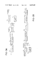
- the word stream of data bits with a parity bit at line 56 is supplied to the serial input of first shift register means 70 having a capacity which is one or multiple words in length.
- first shift register means 70 having a capacity which is one or multiple words in length.
- word stream 20 (FIG. 2) consisting of words having ten (10) data bits and one (1) parity is employed
- shift register means 70 having a capacity which is an integral multiple of eleven (11) bits is employed, and in FIG. 4 an eleven (11) bit capacity shift register means 70 is shown.
- the serial output from the shift register is connected to output line 60 of the parity bit lock-on circuit 12.
- the bit stream 20 simply is shifted through the shift register 70 under control of bit clock pulses 22 at clock input line 58.
- the parallel output lines 72 of shift register means 70 are connected to parallel inputs of parity checker means 74 for checking parity of the eleven (11) bits contained in the register.
- parity checker means 74 is employed depending upon which parity system, i.e. an even or odd parity system, is employed.
- parity checker is checked at each bit interval and, depending upon the results of the parity check a parity "true” or a parity "error" signal is produced at the output line 76 of the parity checker comprising a 1-bit or a 0-bit, respectively.
- parity checker 74 is connected over line 76 to one input of a logic gate 78 shown comprising an AND gate.
- the AND gate output at line 80 is connected to the serial input of a second shift register means 82, with the serial output from said register being connected over line 84 to the second input of said AND gate 78.
- the second shift register means 82 is of the same capacity as register 70, here eleven (11) bits.
- the shift register 82 is clocked by bit clock pulses 22 (FIG. 2) at the same rate as shift register 70.
- the parallel outputs 86 from shift register means 82 are connected to first and second logic gate means 88 and 90, respectively.
- Output line 62 from logic gate 88 is a "one” when input lines 86-1 through 86-10 are “zeros" and line 86-11 is a “one”. With any other combination of inputs, the logic gate 88 output is “zero”.
- Output line 94 from logic gate 90 is a "one” when all input lines 86-1 through 86-11 are “zero”. With any other combination of inputs, i.e. if any one or more input lines is a "one” the output from logic gate 90 is "zero".
- a word clock pulse synchronized with the parity bit is provided at output line 62 from the logic gate 88.
- the word clock pulse is supplied to the reset terminal of a flip-flop 96 to reset the flip-flop if it is in a set condition.
- the Q output goes to a true level which is connected over line 64 to the utilization circuit 66 to signal that the circuit 12 is locked onto the parity bit.
- the output from logic gate 90 which detects when all eleven (11) bits contained in the shift register 82 are "zeros" is connected to the load input terminal of the shift register 82 to load the same with all 1-bits.
- bit lock-on circuit 12 Operation of the parity bit lock-on circuit 12 will best be understood with reference to the waveforms of FIG. 5.
- Bits of the waveforms are shown divided into arbitrary bit groups 1 through 7, with each group consisting of eleven (11) bits numbered 1 through 11. Since each word in the data pulse train consists of ten (10) data bits and a parity bit, it is known that ten of the eleven bits in each group comprise data bits and one comprises the parity bit onto which the circuit locks. Until parity lock-on is achieved, it is not known which bit in the group comprises the parity bit.
- the serial output from the register at line 84 to AND gate 78 will be a 1-bit for at least the first eleven (11) bits.
- the gate output at line 80 is a 1-bit if the parity checker output also is a 1-bit (parity true), and is a 0-bit if the parity checker output is a 0-bit (parity error).
- parity checker output of "zero" is produced when bits 3, 8, 9 and 11 are entered into the data register
- a parity checker output of "one” is produced when bits 7 and 10 are entered (see waveform A).
- Output from logic gate 88 resets flip-flop 96 (waveform F) to signify that parity bit lock-on is achieved.
- a "ones" bit is reinserted into the shift register 82 so long as the parity checker output is true, i.e., is a "one” when the single "ones" contained in shift register 82 is located at the last register stage. Parity checking occurs every eleven bits at which time the logic gate 88 produces a "ones” output if parity is true.
- the probability of parity check N in a non-parity bit slot is 2 -N , and the probability that such a slot is correctly classified non-parity after N tries is (1-2 -N ).
- the probability that all M-1 non-parity slots are correctly classified after N tries is (1 -2 -N ).spsp.M-1. Therefore, the probability, P I , that one or more of the non-parity slots are incorrectly classified after N tries is:
- the probability of lock-on at exactly N tries is the probability that some non-parity slots were incorrectly classified after (N-1) tries times the probability that all were correctly classified after N tries, i.e., ##EQU1##
Abstract
Description
P.sub.I =1-(1-2.sup.-N).sup.M-1. (1)
              TABLE 1
______________________________________
PROBABILITY OF NO LOCK-UP
AFTER N TRIES (M = 11)
        N    P.sub.I
______________________________________
        1    0.999
        2    0.944
        3    0.737
        4    0.476
        5    0.272
        6    0.146
        7    0.075
        8    0.038
        9    0.019
        10   0.010
        11   0.005
        12   0.002
______________________________________
 Table 2 gives P(N) for different values of N and M=11.
              TABLE 2
______________________________________
PROBABILITY OF LOCK-UP
ON THE N.sup.th TRY (M = 11)
        N    P(N)
______________________________________
        2    0.0001
        3    0.0529
        4    0.0938
        5    0.2494
        6    0.1980
        7    0.1246
        8    0.0693
        9    0.0373
        10   0.0188
        11   0.0099
        12   0.0050
______________________________________
 The quantity E(N) has been numerically evaluated for M=11 and is equal to
 5.43.
Claims (25)
Priority Applications (4)
| Application Number | Priority Date | Filing Date | Title |
|---|---|---|---|
| US06/311,783 US4425645A (en) | 1981-10-15 | 1981-10-15 | Digital data transmission with parity bit word lock-on |
| GB08229298A GB2110509B (en) | 1981-10-15 | 1982-10-13 | Apparatus for and methods of processing digital data |
| DE19823238143 DE3238143A1 (en) | 1981-10-15 | 1982-10-14 | DIGITAL DATA TRANSMISSION SYSTEM WITH PARITY BIT WORDING |
| JP57179198A JPS5879352A (en) | 1981-10-05 | 1982-10-14 | Digital data transmitter |
Applications Claiming Priority (1)
| Application Number | Priority Date | Filing Date | Title |
|---|---|---|---|
| US06/311,783 US4425645A (en) | 1981-10-15 | 1981-10-15 | Digital data transmission with parity bit word lock-on |
Publications (1)
| Publication Number | Publication Date |
|---|---|
| US4425645A true US4425645A (en) | 1984-01-10 |
Family
ID=23208450
Family Applications (1)
| Application Number | Title | Priority Date | Filing Date |
|---|---|---|---|
| US06/311,783 Expired - Fee Related US4425645A (en) | 1981-10-05 | 1981-10-15 | Digital data transmission with parity bit word lock-on |
Country Status (4)
| Country | Link |
|---|---|
| US (1) | US4425645A (en) |
| JP (1) | JPS5879352A (en) |
| DE (1) | DE3238143A1 (en) |
| GB (1) | GB2110509B (en) |
Cited By (20)
| Publication number | Priority date | Publication date | Assignee | Title |
|---|---|---|---|---|
| US4507779A (en) * | 1981-05-19 | 1985-03-26 | Ibm Corporation | Medium speed multiples data |
| US4507783A (en) * | 1983-02-28 | 1985-03-26 | At&T Bell Laboratories | Error detection circuitry for digital systems |
| US4524445A (en) * | 1981-10-15 | 1985-06-18 | Victor Company Of Japan, Limited | Method and circuit arrangement for synchronous detection |
| US4551836A (en) * | 1983-06-22 | 1985-11-05 | Gte Automatic Electric Incorporated | Cross-copy arrangement for synchronizing error detection clock signals in a duplex digital system |
| US4680765A (en) * | 1985-07-26 | 1987-07-14 | Doland George D | Autosync circuit for error correcting block decoders |
| WO1992020174A1 (en) * | 1991-05-09 | 1992-11-12 | Codex Corporation | Device and method for asynchronous cyclic redundancy checking for digital receivers |
| US5247616A (en) * | 1989-10-23 | 1993-09-21 | International Business Machines Corporation | Computer system having different communications facilities and data transfer processes between different computers |
| US5374927A (en) * | 1992-12-23 | 1994-12-20 | Honeywell Inc. | Bit-serial decoder for a specially encoded bit stream |
| US5689692A (en) * | 1992-12-23 | 1997-11-18 | Honeywell Inc. | Method and apparatus for decoding an encoded NRZ signal |
| US6021162A (en) * | 1997-10-01 | 2000-02-01 | Rosemount Inc. | Vortex serial communications |
| US6351489B1 (en) | 1996-09-30 | 2002-02-26 | Rosemount Inc. | Data bus communication technique for field instrument |
| US20090045921A1 (en) * | 2007-08-16 | 2009-02-19 | Farpointe Data, Inc., A California Corporation | System and method for multi-protocol radio-frequency identification |
| US20090045913A1 (en) * | 2007-08-16 | 2009-02-19 | Farpointe Data, Inc., A California Corporation | System and method for interrogation radio-frequency identification |
| US20090153290A1 (en) * | 2007-12-14 | 2009-06-18 | Farpointe Data, Inc., A California Corporation | Secure interface for access control systems |
| US20100034375A1 (en) * | 2008-08-11 | 2010-02-11 | Assa Abloy Ab | Secure wiegand communications |
| US20100039220A1 (en) * | 2008-08-14 | 2010-02-18 | Assa Abloy Ab | Rfid reader with embedded attack detection heuristics |
| US20100207740A1 (en) * | 2009-02-19 | 2010-08-19 | FP Wireless, LLC | Long Range Radio Frequency Identification System |
| USRE44466E1 (en) | 1995-12-07 | 2013-08-27 | Koninklijke Philips Electronics N.V. | Method and device for packaging audio samples of a non-PCM encoded audio bitstream into a sequence of frames |
| US8680966B2 (en) | 2009-02-19 | 2014-03-25 | FP Wireless, LLC | Long range radio frequency identification system |
| US10452877B2 (en) | 2016-12-16 | 2019-10-22 | Assa Abloy Ab | Methods to combine and auto-configure wiegand and RS485 |
Families Citing this family (3)
| Publication number | Priority date | Publication date | Assignee | Title |
|---|---|---|---|---|
| JPS62150944A (en) * | 1985-12-24 | 1987-07-04 | Nec Corp | Code error detection system |
| JPS631128A (en) * | 1986-06-20 | 1988-01-06 | Fujitsu Ltd | Synchronizing control system |
| JPS63108828A (en) * | 1986-10-25 | 1988-05-13 | Nippon Telegr & Teleph Corp <Ntt> | Monitoring method for digital line |
Citations (11)
| Publication number | Priority date | Publication date | Assignee | Title |
|---|---|---|---|---|
| US3587043A (en) | 1969-04-29 | 1971-06-22 | Rca Corp | Character parity synchronizer |
| GB1287093A (en) | 1968-08-22 | 1972-08-31 | Plessey Co Ltd | Improvements in or relating to data transmission |
| GB1360148A (en) | 1971-09-23 | 1974-07-17 | Siemens Ag | Devices for synchronising telegraph signals |
| US3842399A (en) | 1974-01-02 | 1974-10-15 | Bell Telephone Labor Inc | Repetitive byte recognition circuit |
| GB1374357A (en) | 1971-03-18 | 1974-11-20 | Siemens Ag | Data transmission systems |
| GB1409184A (en) | 1973-09-27 | 1975-10-08 | Standard Telephones Cables Ltd | Data transmission systems |
| GB1410921A (en) | 1971-11-17 | 1975-10-22 | Gen Electric Co Ltd | Data terminals |
| US3938086A (en) | 1974-04-11 | 1976-02-10 | Societa Italiana Telecomunicazioni Siemens S.P.A. | Circuit arrangement for correcting slip errors in pcm receivers |
| GB1468999A (en) | 1973-12-27 | 1977-03-30 | Sits Soc It Telecom Siemens | Circuit arrangements for the correction of slip error in data transmission systems using cyclic codes |
| US4218770A (en) | 1978-09-08 | 1980-08-19 | Bell Telephone Laboratories, Incorporated | Delay modulation data transmission system |
| US4361898A (en) | 1980-01-09 | 1982-11-30 | Polygram Gmbh | Digital synchronizing system |
-
1981
- 1981-10-15 US US06/311,783 patent/US4425645A/en not_active Expired - Fee Related
-
1982
- 1982-10-13 GB GB08229298A patent/GB2110509B/en not_active Expired
- 1982-10-14 JP JP57179198A patent/JPS5879352A/en active Pending
- 1982-10-14 DE DE19823238143 patent/DE3238143A1/en not_active Withdrawn
Patent Citations (12)
| Publication number | Priority date | Publication date | Assignee | Title |
|---|---|---|---|---|
| GB1287093A (en) | 1968-08-22 | 1972-08-31 | Plessey Co Ltd | Improvements in or relating to data transmission |
| US3587043A (en) | 1969-04-29 | 1971-06-22 | Rca Corp | Character parity synchronizer |
| GB1374357A (en) | 1971-03-18 | 1974-11-20 | Siemens Ag | Data transmission systems |
| GB1360148A (en) | 1971-09-23 | 1974-07-17 | Siemens Ag | Devices for synchronising telegraph signals |
| GB1410921A (en) | 1971-11-17 | 1975-10-22 | Gen Electric Co Ltd | Data terminals |
| GB1409184A (en) | 1973-09-27 | 1975-10-08 | Standard Telephones Cables Ltd | Data transmission systems |
| GB1468999A (en) | 1973-12-27 | 1977-03-30 | Sits Soc It Telecom Siemens | Circuit arrangements for the correction of slip error in data transmission systems using cyclic codes |
| US3842399A (en) | 1974-01-02 | 1974-10-15 | Bell Telephone Labor Inc | Repetitive byte recognition circuit |
| US3938086A (en) | 1974-04-11 | 1976-02-10 | Societa Italiana Telecomunicazioni Siemens S.P.A. | Circuit arrangement for correcting slip errors in pcm receivers |
| GB1507093A (en) | 1974-04-11 | 1978-04-12 | Siemens Spa Italiana | Arrangements for correcting slip errors in pulse-code transmission systems |
| US4218770A (en) | 1978-09-08 | 1980-08-19 | Bell Telephone Laboratories, Incorporated | Delay modulation data transmission system |
| US4361898A (en) | 1980-01-09 | 1982-11-30 | Polygram Gmbh | Digital synchronizing system |
Cited By (29)
| Publication number | Priority date | Publication date | Assignee | Title |
|---|---|---|---|---|
| US4507779A (en) * | 1981-05-19 | 1985-03-26 | Ibm Corporation | Medium speed multiples data |
| US4524445A (en) * | 1981-10-15 | 1985-06-18 | Victor Company Of Japan, Limited | Method and circuit arrangement for synchronous detection |
| US4507783A (en) * | 1983-02-28 | 1985-03-26 | At&T Bell Laboratories | Error detection circuitry for digital systems |
| US4551836A (en) * | 1983-06-22 | 1985-11-05 | Gte Automatic Electric Incorporated | Cross-copy arrangement for synchronizing error detection clock signals in a duplex digital system |
| US4680765A (en) * | 1985-07-26 | 1987-07-14 | Doland George D | Autosync circuit for error correcting block decoders |
| US5247616A (en) * | 1989-10-23 | 1993-09-21 | International Business Machines Corporation | Computer system having different communications facilities and data transfer processes between different computers |
| US5267249A (en) * | 1991-05-09 | 1993-11-30 | Codex Corporation | Device and method for asynchronous cyclic redundancy checking for digital receivers |
| AU646581B2 (en) * | 1991-05-09 | 1994-02-24 | Motorola, Inc. | Device and method for asynchronous cyclic redundancy checking for digital receivers |
| WO1992020174A1 (en) * | 1991-05-09 | 1992-11-12 | Codex Corporation | Device and method for asynchronous cyclic redundancy checking for digital receivers |
| US5374927A (en) * | 1992-12-23 | 1994-12-20 | Honeywell Inc. | Bit-serial decoder for a specially encoded bit stream |
| US5689692A (en) * | 1992-12-23 | 1997-11-18 | Honeywell Inc. | Method and apparatus for decoding an encoded NRZ signal |
| USRE44466E1 (en) | 1995-12-07 | 2013-08-27 | Koninklijke Philips Electronics N.V. | Method and device for packaging audio samples of a non-PCM encoded audio bitstream into a sequence of frames |
| USRE44955E1 (en) | 1995-12-07 | 2014-06-17 | Koninklijke Philips N.V. | Method and device for packaging audio samples of a non-PCM encoded audio bitstream into a sequence of frames |
| US6351489B1 (en) | 1996-09-30 | 2002-02-26 | Rosemount Inc. | Data bus communication technique for field instrument |
| US6021162A (en) * | 1997-10-01 | 2000-02-01 | Rosemount Inc. | Vortex serial communications |
| US20090045913A1 (en) * | 2007-08-16 | 2009-02-19 | Farpointe Data, Inc., A California Corporation | System and method for interrogation radio-frequency identification |
| US8411764B2 (en) | 2007-08-16 | 2013-04-02 | Farpointe Data, Inc. | System and method for multi-protocol radio-frequency identification |
| US20090045921A1 (en) * | 2007-08-16 | 2009-02-19 | Farpointe Data, Inc., A California Corporation | System and method for multi-protocol radio-frequency identification |
| US8624710B2 (en) | 2007-08-16 | 2014-01-07 | Farpointe Data, Inc. | System and method for interrogation radio-frequency identification |
| US20090153290A1 (en) * | 2007-12-14 | 2009-06-18 | Farpointe Data, Inc., A California Corporation | Secure interface for access control systems |
| US8358783B2 (en) | 2008-08-11 | 2013-01-22 | Assa Abloy Ab | Secure wiegand communications |
| US20100034375A1 (en) * | 2008-08-11 | 2010-02-11 | Assa Abloy Ab | Secure wiegand communications |
| US8923513B2 (en) | 2008-08-11 | 2014-12-30 | Assa Abloy Ab | Secure wiegand communications |
| US8943562B2 (en) | 2008-08-11 | 2015-01-27 | Assa Abloy Ab | Secure Wiegand communications |
| US20100039220A1 (en) * | 2008-08-14 | 2010-02-18 | Assa Abloy Ab | Rfid reader with embedded attack detection heuristics |
| US8310344B2 (en) | 2009-02-19 | 2012-11-13 | FP Wireless, LLC | Long range radio frequency identification system |
| US20100207740A1 (en) * | 2009-02-19 | 2010-08-19 | FP Wireless, LLC | Long Range Radio Frequency Identification System |
| US8680966B2 (en) | 2009-02-19 | 2014-03-25 | FP Wireless, LLC | Long range radio frequency identification system |
| US10452877B2 (en) | 2016-12-16 | 2019-10-22 | Assa Abloy Ab | Methods to combine and auto-configure wiegand and RS485 |
Also Published As
| Publication number | Publication date |
|---|---|
| DE3238143A1 (en) | 1983-04-28 |
| JPS5879352A (en) | 1983-05-13 |
| GB2110509B (en) | 1986-08-13 |
| GB2110509A (en) | 1983-06-15 |
Similar Documents
| Publication | Publication Date | Title |
|---|---|---|
| US4425645A (en) | Digital data transmission with parity bit word lock-on | |
| US4506372A (en) | Method and apparatus for recognizing in a receiver the start of a telegram signal consisting of a bit impulse sequence | |
| US4387460A (en) | Supplementary information transmitting arrangement for a digital data transmission system | |
| US4216460A (en) | Transmission and/or recording of digital signals | |
| US4337458A (en) | Data encoding method and system employing two-thirds code rate with full word look-ahead | |
| US3767855A (en) | Pulse position modulation communication system | |
| CA1188001A (en) | Device for processing serial information which includes synchronization words | |
| US4146909A (en) | Sync pattern encoding system for run-length limited codes | |
| US4301534A (en) | Framing circuit for time multiplexed data | |
| CA1318004C (en) | Single track orthogonal error correction system | |
| US4072987A (en) | Digital storage systems | |
| EP0118121B1 (en) | Improvements in or relating to an apparatus for encoding and decoding sequential information in data handling systems | |
| US4562581A (en) | Digital signal transmitting and receiving system for serial data which can be easily decoded | |
| US4410990A (en) | Processing binary data | |
| US3215779A (en) | Digital data conversion and transmission system | |
| US4500871A (en) | Method for coding binary data and a device decoding coded data | |
| US3230310A (en) | Biternary pulse code system | |
| US4087642A (en) | Digital data communication system | |
| US6084536A (en) | Conversion of a sequence of m-bit information words into a modulated signal | |
| US4352129A (en) | Digital recording apparatus | |
| US4766602A (en) | Synchronizing signal decoding | |
| US4481648A (en) | Method and system for producing a synchronous signal from _cyclic-redundancy-coded digital data blocks | |
| US4573172A (en) | Programmable circuit for series-parallel transformation of a digital signal | |
| US4709227A (en) | Method and device for inserting a digital signal in a channel with higher flow rate | |
| US5093830A (en) | Self-synchronizing serial transmission of signaling bits in a digital switch |
Legal Events
| Date | Code | Title | Description |
|---|---|---|---|
| AS | Assignment |
Owner name: SRI INTERNATIONAL; MENLO PARK, CA. A CORP. OF CA. Free format text: ASSIGNMENT OF ASSIGNORS INTEREST.;ASSIGNORS:WEAVER, CHARLES S.;YARBOROUGH, JOHN M. JR.;REEL/FRAME:003935/0689 Effective date: 19811002 |
|
| MAFP | Maintenance fee payment |
Free format text: PAYMENT OF MAINTENANCE FEE, 4TH YEAR, PL 96-517 (ORIGINAL EVENT CODE: M170); ENTITY STATUS OF PATENT OWNER: SMALL ENTITY Year of fee payment: 4 |
|
| FEPP | Fee payment procedure |
Free format text: PAYOR NUMBER ASSIGNED (ORIGINAL EVENT CODE: ASPN); ENTITY STATUS OF PATENT OWNER: SMALL ENTITY |
|
| FEPP | Fee payment procedure |
Free format text: MAINTENANCE FEE REMINDER MAILED (ORIGINAL EVENT CODE: REM.); ENTITY STATUS OF PATENT OWNER: SMALL ENTITY |
|
| FEPP | Fee payment procedure |
Free format text: SURCHARGE FOR LATE PAYMENT, PL 96-517 (ORIGINAL EVENT CODE: M176); ENTITY STATUS OF PATENT OWNER: SMALL ENTITY |
|
| MAFP | Maintenance fee payment |
Free format text: PAYMENT OF MAINTENANCE FEE, 8TH YEAR, PL 96-517 (ORIGINAL EVENT CODE: M171); ENTITY STATUS OF PATENT OWNER: SMALL ENTITY Year of fee payment: 8 |
|
| FEPP | Fee payment procedure |
Free format text: MAINTENANCE FEE REMINDER MAILED (ORIGINAL EVENT CODE: REM.); ENTITY STATUS OF PATENT OWNER: SMALL ENTITY |
|
| LAPS | Lapse for failure to pay maintenance fees | ||
| FP | Lapsed due to failure to pay maintenance fee |
Effective date: 19960110 |
|
| STCH | Information on status: patent discontinuation |
Free format text: PATENT EXPIRED DUE TO NONPAYMENT OF MAINTENANCE FEES UNDER 37 CFR 1.362 |