US4430594A - Device for contacting tubular piezo-electric transducers - Google Patents

Device for contacting tubular piezo-electric transducers Download PDF

Info

Publication number
US4430594A
US4430594A US06/465,120 US46512083A US4430594A US 4430594 A US4430594 A US 4430594A US 46512083 A US46512083 A US 46512083A US 4430594 A US4430594 A US 4430594A
Authority
US
United States
Prior art keywords
elements
contacting
transducer
contact
feedthrough
Prior art date
Legal status (The legal status is an assumption and is not a legal conclusion. Google has not performed a legal analysis and makes no representation as to the accuracy of the status listed.)
Expired - Fee Related
Application number
US06/465,120
Inventor
Klaus Bork
Rolf Humbs
Karl Trey
Current Assignee (The listed assignees may be inaccurate. Google has not performed a legal analysis and makes no representation or warranty as to the accuracy of the list.)
Siemens AG
Original Assignee
Siemens AG
Priority date (The priority date is an assumption and is not a legal conclusion. Google has not performed a legal analysis and makes no representation as to the accuracy of the date listed.)
Filing date
Publication date
Application filed by Siemens AG filed Critical Siemens AG
Assigned to SIEMENS AKTIENGESELLSCHAFT A GERMAN CORP. reassignment SIEMENS AKTIENGESELLSCHAFT A GERMAN CORP. ASSIGNMENT OF ASSIGNORS INTEREST. Assignors: BORK, KLAUS, HUMBS, ROLF, TREY, KARL
Application granted granted Critical
Publication of US4430594A publication Critical patent/US4430594A/en
Anticipated expiration legal-status Critical
Expired - Fee Related legal-status Critical Current

Links

Images

Classifications

    • BPERFORMING OPERATIONS; TRANSPORTING
    • B41PRINTING; LINING MACHINES; TYPEWRITERS; STAMPS
    • B41JTYPEWRITERS; SELECTIVE PRINTING MECHANISMS, i.e. MECHANISMS PRINTING OTHERWISE THAN FROM A FORME; CORRECTION OF TYPOGRAPHICAL ERRORS
    • B41J2/00Typewriters or selective printing mechanisms characterised by the printing or marking process for which they are designed
    • B41J2/005Typewriters or selective printing mechanisms characterised by the printing or marking process for which they are designed characterised by bringing liquid or particles selectively into contact with a printing material
    • B41J2/01Ink jet
    • B41J2/135Nozzles
    • B41J2/14Structure thereof only for on-demand ink jet heads
    • B41J2/14201Structure of print heads with piezoelectric elements
    • B41J2/1429Structure of print heads with piezoelectric elements of tubular type
    • HELECTRICITY
    • H10SEMICONDUCTOR DEVICES; ELECTRIC SOLID-STATE DEVICES NOT OTHERWISE PROVIDED FOR
    • H10NELECTRIC SOLID-STATE DEVICES NOT OTHERWISE PROVIDED FOR
    • H10N30/00Piezoelectric or electrostrictive devices
    • H10N30/80Constructional details
    • H10N30/87Electrodes or interconnections, e.g. leads or terminals
    • H10N30/875Further connection or lead arrangements, e.g. flexible wiring boards, terminal pins

Definitions

  • the present invention is directed to a device for contacting each of a plurality of tubular piezo-electric transducer elements which are arranged in rows and encapsulated in a synthetic material to form a printing head for an ink printing device.
  • a device for contacting tubular piezo-electric transducer elements in a printing head of an ink printing device is disclosed in German OS 27 40 773.
  • the transducer elements are disposed in rows and diverge radiantly from an ink discharge opening with the diverging elements being encapsulated in a synthetic material such as plastic.
  • the device for contacting and positioning consist of a sheet-like flexible conductive film on which the transducer elements that are to be contacted are disposed and contacted by wire helixes which are received on the inside of each of the transducer elements. The outer surface of each of the elements is contacted by a solder connection.
  • the entire arrangement of foils is then encapsulated in a synthetic material or plastic with wire segments or mandrels being temporarily placed to extend through each of the transducer elements to maintain the desired position for the elements and after the synthetic material has been cured, these wire segments or mandrels are removed to form the ink channels.
  • the above described manufacturing method is relatively expensive. Since automation of the manufacturing process can only be conditionally possible, it is very expensive when adapted to a mass production process.
  • the present invention is directed to providing a device for contacting each of a plurality of tubular piezo-electric transducer elements which are arranged in rows and encapsulated in synthetic material to form a printing head for an ink printing device which contacting device enables an extensive automation of the assembly procedures and operations and simplifies the manufacturing of the printing head.
  • the device for contacting each of the plurality of tubular piezo-electrical transducer elements which are arranged in rows and encapsulated in synthetic material to form the printing head comprises a printed circuit board; a first contacting element and a second contacting element for each transducer element, each of the first contacting elements consisting of an inside contact sleeve having a contact surface resiliently pressing against an inside wall surface of the transducer element, said inside contact sleeve being connected to a flexible spacer extending out of the transducer element, each of the second contact elements comprising a resilient connector with a resilient clamp for elastically embracing the outside of the transducer element extending therefrom, said circuit board having a row of feedthrough holes for each row of elements with one feedthrough hole for each of the transducer elements, each feedthrough hole having a first acceptance open extending into an electrical conductor path and a second acceptance opening extending into a different conductor path; means for securing the flexible spacer of each first conductor element in the first
  • the present invention makes it possible to automatically equip each of the transducer elements which consist of a piezo-electrical hollow tube with stamped contacting elements and to then assemble the piezo-electric tubes to extend at right angles into the printed circuit board which is provided with the acceptance openings for each of the contacting elements. After insertion of the contacting elements into the acceptance openings of the printed circuit board, they can be connected by either a soldering process such as flow solder or drag solder to the various conductor paths.
  • All contacting elements are elastically designed in their base areas so that an oblique attitude of the transducer element required for the printhead assembly in the casting process is possible.
  • the temporary wire segments or mandrels which are required in the casting process for producing the ink channels, can be threaded through the printed circuit board into each of the transducer elements to thereby assure alignment between the openings provided in the circuit board and the transducer elements. After the encapsulating process, these wire segments are again removed as in the previously known process.
  • FIGURE is a side view of an embodiment of the device of the present invention with portions in cross-section for purposes of illustration.
  • the principles of the present invention are particularly useful for positioning a plurality of piezo-electric transducer elements 1 in rows on a printed circuit board 9 prior to encapsulation to form a printing head.
  • each of the tubular piezo-electric elements 1 of a printing head of an ink printing device are arranged in a row and will be subsequently encapsulated in a synthetic material such as a synthetic plastic.
  • a synthetic material such as a synthetic plastic.
  • two contacting elements namely, a first contacting element 2 and a second contacting element 3 are utilized.
  • Both the contacting elements 2 and 3 are single one-piece members and are manufactured from sheet metal by a stamping method.
  • the first contacting element 2 will have an inside contacting sleeve 4 having a contact surface 5 which is pressed radially elastically against the inside wall surface of the transducer element 1.
  • the contact sleeve 4 is connected to a flexible spacer 6 which will extend out of the tubular element 1 and as illustrated has a right angle bend forming a shoulder 15.
  • the second contacting element 3 has a resilient connector 7 and a resilient clamp portion 8 which elastically embraces the outside surface of the transducer element.
  • the clamp element 8 is biased to grip the outside surface of the element 1 while the contacting sleeve 4 is biased to grip the inside wall surface.
  • an automated device which is not illustrated will assemble the contacting elements 2 and 3 on the transducer elements 1.
  • the first contact element 2 is designed to be inserted into the transducer element and make contact with the inside surface due to the resilient nature of the sleeve portion 4 while the clamp 8 of the second contact element will grip the outside of the sleeve 1.
  • the printed circuit board 9 will have a plurality of conductor paths 10 and 10' which can receive the driving currents for the transducer elements. As illustrated, the printed circuit board 9 has a row of feedthrough holes 11 which form part of the ink channels for the transducer elements. Each of the feedthrough holes 11 has a first acceptance opening 12 and a second acceptance opening 12'. The acceptance openings 12 and 12' are arranged adjacent to their feedthrough hole 11 and extend through conductor paths 10 and 10', respectively.
  • the contact elements 2 and 3 with their respective transducer element 1 are assembled on the board by the flexible spacer 6 being inserted into the opening 12 and the resilient conductor 7 being inserted into the opening 12'.
  • the central opening of each of the elements 11 will be positioned in alignment directly above the feedthrough hole 11 at a distance a. This distance is maintained or selected by the position of the shoulder 15.
  • a soldering process such as a flow or drag soldering is carried out to electrically connect the path 10 to the flexible spacer 6 and the path 10' to the resilient connector 7.
  • the elastic design of the flexible spacer 6 of the first contact element 2 having the shoulder 15 serves as a spacer in conjunction with the resilient connector 7 of the second contacting element. Due to the elastic nature of both the connector 7 and the spacer 6, the transducer element 1 can be pivoted around an angle ⁇ during the subsequent assembly of the print head. To this end, wire segments or mandrels are placed through the feed hole 11 and through the center openings in each of the elements 1 to obtain the desired alignment of the transducer element with the opening 11 and the desired aim of the ink channels when the arrangement of elements 1 on the board 9 are encapsulated.
  • the design of the contacting elements should be to improve the elastic properties.
  • the portions of each of the elements which create the contact with the transducer element are designed in such a term that with regard to their contact force that no plastic flow or creep should occur in the contacting area during the elevated temperatures involved with the encapsulation.

Abstract

A contacting device for electrically connecting rows of tubular piezo transducers of a printing head of an ink printing device consisting of a printed circuit board having separate conductor paths, a row of feedthrough holes for each row of transducer elements with one hole for each element, a first contact element having an inside contact sleeve biased against the inside wall of the transducer element and a flexible spacer extending therefrom and through an opening in the board adjacent the feedthrough hole, a second contacting element having a resilient connector supporting a resilient clamp for embracing the outer surface of the element being mounted in another hole adjacent the feedthrough opening with both the elastic spacer and the resilient connector being soldered to the conductor paths so that the element is positioned above the feedthrough hole and an electrical current can be applied to the transducer.

Description

BACKGROUND OF THE INVENTION
The present invention is directed to a device for contacting each of a plurality of tubular piezo-electric transducer elements which are arranged in rows and encapsulated in a synthetic material to form a printing head for an ink printing device.
A device for contacting tubular piezo-electric transducer elements in a printing head of an ink printing device is disclosed in German OS 27 40 773. In this device, the transducer elements are disposed in rows and diverge radiantly from an ink discharge opening with the diverging elements being encapsulated in a synthetic material such as plastic. The device for contacting and positioning consist of a sheet-like flexible conductive film on which the transducer elements that are to be contacted are disposed and contacted by wire helixes which are received on the inside of each of the transducer elements. The outer surface of each of the elements is contacted by a solder connection. Subsequent to securing each of the elements on the foil, the entire arrangement of foils is then encapsulated in a synthetic material or plastic with wire segments or mandrels being temporarily placed to extend through each of the transducer elements to maintain the desired position for the elements and after the synthetic material has been cured, these wire segments or mandrels are removed to form the ink channels.
The above described manufacturing method is relatively expensive. Since automation of the manufacturing process can only be conditionally possible, it is very expensive when adapted to a mass production process.
SUMMARY OF THE INVENTION
The present invention is directed to providing a device for contacting each of a plurality of tubular piezo-electric transducer elements which are arranged in rows and encapsulated in synthetic material to form a printing head for an ink printing device which contacting device enables an extensive automation of the assembly procedures and operations and simplifies the manufacturing of the printing head.
To accomplish these goals, the device for contacting each of the plurality of tubular piezo-electrical transducer elements which are arranged in rows and encapsulated in synthetic material to form the printing head comprises a printed circuit board; a first contacting element and a second contacting element for each transducer element, each of the first contacting elements consisting of an inside contact sleeve having a contact surface resiliently pressing against an inside wall surface of the transducer element, said inside contact sleeve being connected to a flexible spacer extending out of the transducer element, each of the second contact elements comprising a resilient connector with a resilient clamp for elastically embracing the outside of the transducer element extending therefrom, said circuit board having a row of feedthrough holes for each row of elements with one feedthrough hole for each of the transducer elements, each feedthrough hole having a first acceptance open extending into an electrical conductor path and a second acceptance opening extending into a different conductor path; means for securing the flexible spacer of each first conductor element in the first opening and in electrical contact with the conductor path associated therewith and means for securing each of the resilient connectors of the second conductor elements in the respective second openings and in electrical contact with the conductor path associated therewith so that each of the transducer elements were situated a fixed distance from each of the feed holes and aligned therewith.
The present invention makes it possible to automatically equip each of the transducer elements which consist of a piezo-electrical hollow tube with stamped contacting elements and to then assemble the piezo-electric tubes to extend at right angles into the printed circuit board which is provided with the acceptance openings for each of the contacting elements. After insertion of the contacting elements into the acceptance openings of the printed circuit board, they can be connected by either a soldering process such as flow solder or drag solder to the various conductor paths.
All contacting elements are elastically designed in their base areas so that an oblique attitude of the transducer element required for the printhead assembly in the casting process is possible. The temporary wire segments or mandrels, which are required in the casting process for producing the ink channels, can be threaded through the printed circuit board into each of the transducer elements to thereby assure alignment between the openings provided in the circuit board and the transducer elements. After the encapsulating process, these wire segments are again removed as in the previously known process.
BRIEF DESCRIPTION OF THE DRAWING
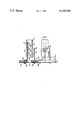
The FIGURE is a side view of an embodiment of the device of the present invention with portions in cross-section for purposes of illustration.
DESCRIPTION OF THE PREFERRED EMBODIMENTS
The principles of the present invention are particularly useful for positioning a plurality of piezo-electric transducer elements 1 in rows on a printed circuit board 9 prior to encapsulation to form a printing head.
As illustrated, each of the tubular piezo-electric elements 1 of a printing head of an ink printing device are arranged in a row and will be subsequently encapsulated in a synthetic material such as a synthetic plastic. To position each of the elements 1, two contacting elements, namely, a first contacting element 2 and a second contacting element 3 are utilized. Both the contacting elements 2 and 3 are single one-piece members and are manufactured from sheet metal by a stamping method. The first contacting element 2 will have an inside contacting sleeve 4 having a contact surface 5 which is pressed radially elastically against the inside wall surface of the transducer element 1. The contact sleeve 4 is connected to a flexible spacer 6 which will extend out of the tubular element 1 and as illustrated has a right angle bend forming a shoulder 15. The second contacting element 3 has a resilient connector 7 and a resilient clamp portion 8 which elastically embraces the outside surface of the transducer element. Thus, the clamp element 8 is biased to grip the outside surface of the element 1 while the contacting sleeve 4 is biased to grip the inside wall surface.
In an automated process, an automated device which is not illustrated will assemble the contacting elements 2 and 3 on the transducer elements 1. Thus, the first contact element 2 is designed to be inserted into the transducer element and make contact with the inside surface due to the resilient nature of the sleeve portion 4 while the clamp 8 of the second contact element will grip the outside of the sleeve 1.
The printed circuit board 9 will have a plurality of conductor paths 10 and 10' which can receive the driving currents for the transducer elements. As illustrated, the printed circuit board 9 has a row of feedthrough holes 11 which form part of the ink channels for the transducer elements. Each of the feedthrough holes 11 has a first acceptance opening 12 and a second acceptance opening 12'. The acceptance openings 12 and 12' are arranged adjacent to their feedthrough hole 11 and extend through conductor paths 10 and 10', respectively.
The contact elements 2 and 3 with their respective transducer element 1 are assembled on the board by the flexible spacer 6 being inserted into the opening 12 and the resilient conductor 7 being inserted into the opening 12'. In such an arrangement, the central opening of each of the elements 11 will be positioned in alignment directly above the feedthrough hole 11 at a distance a. This distance is maintained or selected by the position of the shoulder 15. After insertion of the contact elements into the respective acceptance holes 12 and 12' of the printed circuit board, a soldering process such as a flow or drag soldering is carried out to electrically connect the path 10 to the flexible spacer 6 and the path 10' to the resilient connector 7.
The elastic design of the flexible spacer 6 of the first contact element 2 having the shoulder 15 serves as a spacer in conjunction with the resilient connector 7 of the second contacting element. Due to the elastic nature of both the connector 7 and the spacer 6, the transducer element 1 can be pivoted around an angle α during the subsequent assembly of the print head. To this end, wire segments or mandrels are placed through the feed hole 11 and through the center openings in each of the elements 1 to obtain the desired alignment of the transducer element with the opening 11 and the desired aim of the ink channels when the arrangement of elements 1 on the board 9 are encapsulated.
Other embodiments are conceivable for designing the contact elements. Thus, it is possible to design the inner contact sleeve 4 of the contact element 2 so that it consists of a half spiral fan comb-like which can be stamped in a particularly simple manner. Additional slits such as 13 can be provided on the clamps 8 to increase the elasticity so that the clamp will be biased onto the outer surface of the elements 1. The individual fingers being formed therefrom will improve the contactability of each of the connectors 2 and 3.
It should be pointed out that the design of the contacting elements should be to improve the elastic properties. However, the portions of each of the elements which create the contact with the transducer element are designed in such a term that with regard to their contact force that no plastic flow or creep should occur in the contacting area during the elevated temperatures involved with the encapsulation.
Although various minor modifications may be suggested by those versed in the art, it should be understood that we wish to embody within the scope of the patent granted hereon, all such modifications as reasonably and properly come within the scope of our contribution to the art.

Claims (5)

We claim:
1. A device for contacting each of a plurality of tubular piezo-electrical transducer elements which are arranged in rows and encapsulated in a synthetic material to form a printing head for an ink printing device, said device comprising a printed circuit board; a first contacting element and a second contacting element for each transducer element, each of the first contacting elements consisting of an inside contact sleeve having a contact surface resiliently pressing against an inside wall surface of a transducer element, said inside contact sleeve being connected to a flexible spacer extending out of the transducer element, each of the second contact elements comprising a resilient connector with a resilient clamp for elastically embracing the outside of the transducer element extending therefrom, said circuit board having a row of feedthrough holes for each row of elements with one feedthrough hole for each of the transducer elements, each feedthrough hole having a first acceptance opening extending into an electrical conductor path and a second acceptance opening extending into a different conductor path; means for securing the flexible spacer of each first conducting element in the first openings and in electrical contact with the conductor path associated therewith; and means for securing each of the resilient connectors of the second conducting elements in the respective second openings and in electrical contact with the conductor path associated therewith so that each of the transducer elements are situated at a fixed distance from each of the feedthrough holes and aligned therewith.
2. A device according to claim 1, wherein the inside contact sleeve of each of the first contacting elements consist of a half-spiral fanned comb-like piece of sheet metal.
3. A device according to claim 1, wherein each of the first and second contact elements consist of a single stamped metal piece.
4. A device according to claim 3, wherein the inside contact sleeve of each of the first contact elements has a half-spiral fanned comb-like shape.
5. A device according to claim 1, wherein each of the flexible spacers has at least one right angle bend to form a shoulder to establish the desired spacing of the transducer element from the circuit board.
US06/465,120 1982-03-10 1983-02-09 Device for contacting tubular piezo-electric transducers Expired - Fee Related US4430594A (en)

Applications Claiming Priority (2)

Application Number Priority Date Filing Date Title
DE19823208679 DE3208679A1 (en) 1982-03-10 1982-03-10 DEVICE FOR CONTACTING TUBE-SHAPED PIEZWALKERS TO BE PLASTED IN PLASTIC
DE3208679 1982-03-10

Publications (1)

Publication Number Publication Date
US4430594A true US4430594A (en) 1984-02-07

Family

ID=6157853

Family Applications (1)

Application Number Title Priority Date Filing Date
US06/465,120 Expired - Fee Related US4430594A (en) 1982-03-10 1983-02-09 Device for contacting tubular piezo-electric transducers

Country Status (4)

Country Link
US (1) US4430594A (en)
EP (1) EP0088435A2 (en)
JP (1) JPS58171968A (en)
DE (1) DE3208679A1 (en)

Cited By (4)

* Cited by examiner, † Cited by third party
Publication number Priority date Publication date Assignee Title
EP0161341A2 (en) * 1984-05-18 1985-11-21 Siemens Aktiengesellschaft Device for fastening and contacting for cylindrical piezo-electrical transducers
EP0164445A2 (en) * 1984-05-16 1985-12-18 Siemens Aktiengesellschaft Arrangement for the fixing and the connecting of piezoelectrical drive elements in the print head of an ink jet printer
US4698644A (en) * 1986-10-27 1987-10-06 International Business Machines Drop-on-demand ink jet print head
US5258781A (en) * 1992-04-08 1993-11-02 Xerox Corporation One-step encapsulation, air gap sealing and structure bonding of thermal ink jet printhead

Families Citing this family (1)

* Cited by examiner, † Cited by third party
Publication number Priority date Publication date Assignee Title
JPH03124010A (en) * 1989-10-08 1991-05-27 Murata Mfg Co Ltd Terminal of electronic component

Family Cites Families (2)

* Cited by examiner, † Cited by third party
Publication number Priority date Publication date Assignee Title
DE2543420C3 (en) * 1975-09-29 1980-09-11 Siemens Ag, 1000 Berlin Und 8000 Muenchen Piezoelectric drive element for writing heads in ink mosaic writing devices
DE2740773A1 (en) * 1977-09-09 1979-03-15 Siemens Ag Multiple head ink jet printer - has array of piezoelectric pumps electrically connected by printed circuit foil

Cited By (6)

* Cited by examiner, † Cited by third party
Publication number Priority date Publication date Assignee Title
EP0164445A2 (en) * 1984-05-16 1985-12-18 Siemens Aktiengesellschaft Arrangement for the fixing and the connecting of piezoelectrical drive elements in the print head of an ink jet printer
EP0164445A3 (en) * 1984-05-16 1986-05-21 Siemens Aktiengesellschaft Arrangement for the fixing and the connecting of piezoelectrical drive elements in the print head of an ink jet printer
EP0161341A2 (en) * 1984-05-18 1985-11-21 Siemens Aktiengesellschaft Device for fastening and contacting for cylindrical piezo-electrical transducers
EP0161341A3 (en) * 1984-05-18 1986-10-22 Siemens Aktiengesellschaft Berlin Und Munchen Device for fastening and contacting for cylindrical piezo-electrical transducers
US4698644A (en) * 1986-10-27 1987-10-06 International Business Machines Drop-on-demand ink jet print head
US5258781A (en) * 1992-04-08 1993-11-02 Xerox Corporation One-step encapsulation, air gap sealing and structure bonding of thermal ink jet printhead

Also Published As

Publication number Publication date
DE3208679A1 (en) 1983-09-22
EP0088435A2 (en) 1983-09-14
JPS58171968A (en) 1983-10-08

Similar Documents

Publication Publication Date Title
US4737115A (en) Solderable lead
US4547756A (en) Multiple reed switch module
US3975072A (en) Low profile integrated circuit connector and method
CA2020462A1 (en) Electrical connector device
US5997367A (en) Adapter
JPS60227373A (en) Multicontact connector and method of producing same
EP0712142B1 (en) Electronic thick film component multiple terminal and method of making the same
EP0437606A4 (en) Electrical connectors
US3184532A (en) Electrical component and method of assembly
US4430594A (en) Device for contacting tubular piezo-electric transducers
US4776807A (en) Compliant contact
US4385341A (en) Strain relief member for flat flexible cables
JPH05144484A (en) Insulation rejecting type probe and connector using this probe
US3975078A (en) Folded electrical contact
US2776415A (en) Tube socket for printed wiring panels
US3668604A (en) Strip-type dip receptacle
US4785990A (en) Electronic component with lead terminals and method of manufacturing said electronic component
US5876221A (en) Surface mount contact assembly for printed circuit board
JPH0236242Y2 (en)
JP3340072B2 (en) PCB socket
JPH0617333Y2 (en) Connection terminal for printed wiring board
EP3937597B1 (en) Solder coated rivet electrical connector
CN216773563U (en) Connector with a locking member
US5279508A (en) Shifting connection device
JPH0236241Y2 (en)

Legal Events

Date Code Title Description
AS Assignment

Owner name: SIEMENS AKTIENGESELLSCHAFT BERLIN AND MUNICH A GER

Free format text: ASSIGNMENT OF ASSIGNORS INTEREST.;ASSIGNORS:BORK, KLAUS;HUMBS, ROLF;TREY, KARL;REEL/FRAME:004093/0292

Effective date: 19830117

FEPP Fee payment procedure

Free format text: PAYOR NUMBER ASSIGNED (ORIGINAL EVENT CODE: ASPN); ENTITY STATUS OF PATENT OWNER: LARGE ENTITY

FEPP Fee payment procedure

Free format text: MAINTENANCE FEE REMINDER MAILED (ORIGINAL EVENT CODE: REM.); ENTITY STATUS OF PATENT OWNER: LARGE ENTITY

LAPS Lapse for failure to pay maintenance fees
STCH Information on status: patent discontinuation

Free format text: PATENT EXPIRED DUE TO NONPAYMENT OF MAINTENANCE FEES UNDER 37 CFR 1.362

FP Lapsed due to failure to pay maintenance fee

Effective date: 19880207