US4462090A - Method of operating a semiconductor memory circuit - Google Patents
Method of operating a semiconductor memory circuit Download PDFInfo
- Publication number
- US4462090A US4462090A US06/393,608 US39360882A US4462090A US 4462090 A US4462090 A US 4462090A US 39360882 A US39360882 A US 39360882A US 4462090 A US4462090 A US 4462090A
- Authority
- US
- United States
- Prior art keywords
- gate electrode
- insulation layer
- gate
- memory elements
- drain
- Prior art date
- Legal status (The legal status is an assumption and is not a legal conclusion. Google has not performed a legal analysis and makes no representation as to the accuracy of the status listed.)
- Expired - Lifetime
Links
- 239000004065 semiconductor Substances 0.000 title claims abstract description 21
- 238000000034 method Methods 0.000 title claims description 8
- 238000009413 insulation Methods 0.000 claims abstract description 36
- 239000000758 substrate Substances 0.000 claims abstract description 26
- 230000015654 memory Effects 0.000 claims description 71
- 239000011159 matrix material Substances 0.000 claims description 8
- 239000003795 chemical substances by application Substances 0.000 description 6
- 238000010276 construction Methods 0.000 description 4
- 239000012535 impurity Substances 0.000 description 4
- 230000010354 integration Effects 0.000 description 4
- 238000002347 injection Methods 0.000 description 3
- 239000007924 injection Substances 0.000 description 3
- VYPSYNLAJGMNEJ-UHFFFAOYSA-N Silicium dioxide Chemical compound O=[Si]=O VYPSYNLAJGMNEJ-UHFFFAOYSA-N 0.000 description 2
- 239000000969 carrier Substances 0.000 description 2
- 238000005229 chemical vapour deposition Methods 0.000 description 2
- 230000003247 decreasing effect Effects 0.000 description 2
- 238000009792 diffusion process Methods 0.000 description 2
- 230000000694 effects Effects 0.000 description 2
- 230000005684 electric field Effects 0.000 description 2
- 239000002784 hot electron Substances 0.000 description 2
- 229910021420 polycrystalline silicon Inorganic materials 0.000 description 2
- 229910052710 silicon Inorganic materials 0.000 description 2
- 239000010703 silicon Substances 0.000 description 2
- XUIMIQQOPSSXEZ-UHFFFAOYSA-N Silicon Chemical compound [Si] XUIMIQQOPSSXEZ-UHFFFAOYSA-N 0.000 description 1
- 239000004411 aluminium Substances 0.000 description 1
- 229910052782 aluminium Inorganic materials 0.000 description 1
- XAGFODPZIPBFFR-UHFFFAOYSA-N aluminium Chemical compound [Al] XAGFODPZIPBFFR-UHFFFAOYSA-N 0.000 description 1
- 230000015572 biosynthetic process Effects 0.000 description 1
- 238000010586 diagram Methods 0.000 description 1
- 238000005468 ion implantation Methods 0.000 description 1
- 150000002500 ions Chemical class 0.000 description 1
- 229910052751 metal Inorganic materials 0.000 description 1
- 239000002184 metal Substances 0.000 description 1
- 230000002093 peripheral effect Effects 0.000 description 1
- 239000003870 refractory metal Substances 0.000 description 1
- 238000004904 shortening Methods 0.000 description 1
- 229910021332 silicide Inorganic materials 0.000 description 1
- FVBUAEGBCNSCDD-UHFFFAOYSA-N silicide(4-) Chemical compound [Si-4] FVBUAEGBCNSCDD-UHFFFAOYSA-N 0.000 description 1
- 229910052814 silicon oxide Inorganic materials 0.000 description 1
- 239000007787 solid Substances 0.000 description 1
Images


Classifications
-
- G—PHYSICS
- G11—INFORMATION STORAGE
- G11C—STATIC STORES
- G11C16/00—Erasable programmable read-only memories
- G11C16/02—Erasable programmable read-only memories electrically programmable
- G11C16/04—Erasable programmable read-only memories electrically programmable using variable threshold transistors, e.g. FAMOS
- G11C16/0408—Erasable programmable read-only memories electrically programmable using variable threshold transistors, e.g. FAMOS comprising cells containing floating gate transistors
- G11C16/0425—Erasable programmable read-only memories electrically programmable using variable threshold transistors, e.g. FAMOS comprising cells containing floating gate transistors comprising cells containing a merged floating gate and select transistor
-
- H—ELECTRICITY
- H01—ELECTRIC ELEMENTS
- H01L—SEMICONDUCTOR DEVICES NOT COVERED BY CLASS H10
- H01L29/00—Semiconductor devices adapted for rectifying, amplifying, oscillating or switching, or capacitors or resistors with at least one potential-jump barrier or surface barrier, e.g. PN junction depletion layer or carrier concentration layer; Details of semiconductor bodies or of electrodes thereof ; Multistep manufacturing processes therefor
- H01L29/66—Types of semiconductor device ; Multistep manufacturing processes therefor
- H01L29/68—Types of semiconductor device ; Multistep manufacturing processes therefor controllable by only the electric current supplied, or only the electric potential applied, to an electrode which does not carry the current to be rectified, amplified or switched
- H01L29/76—Unipolar devices, e.g. field effect transistors
- H01L29/772—Field effect transistors
- H01L29/78—Field effect transistors with field effect produced by an insulated gate
- H01L29/788—Field effect transistors with field effect produced by an insulated gate with floating gate
- H01L29/7881—Programmable transistors with only two possible levels of programmation
Definitions
- This invention relates to a semiconductor memory element of MOS type of which the contents may be electrically rewritten and, more particularly, to a memory circuit having the memory elements arranged in a matrix fashion.
- Source and drain regions are formed in a semiconductor substrate of P conductivity type.
- a first electrode as a floating gate electrode is formed on a channel region between the source and the drain region with a first insulation layer interposed between the first electrode and the channel region.
- a second gate electrode as a control gate is further formed on the first gate electrode with a second insulation layer interposed between both.
- a positive voltage (20 V or more) is applied to the control gate electrode while at the same time a positive voltage is applied to the drain.
- the transistor operates in a saturation region. Under this condition, an N-channel is formed between the source and the drain. High energy potential electrons arising from inpact ionization in the N-channel region are injected into the first and second insulation layers and attracted toward the control gate electrode with the positive voltage impressed. At this time, the electrons are trapped by the floating gate electrode so that the N-channel disappears and the MOS transistor is turned off.
- the write operation is carried out as described above.
- the read operation is at relatively high speed, but the write operation is at low speed, that is to say, it takes a relatively long time, about 2 ms.
- the voltages applied to the drain and the control gate in the write operation is high, e.g. 20 V or more. This is disadvantageous in fabricating the memory device having the memory elements of this type with high density and large memory capacity.
- the floating gate electrode is greatly extended into the field region so that a capacitance between the control gate and the floating gate can be larger than that between the floating gate and the substrate and the electric field in the first insulation layer becomes large enough to increase the electron injection.
- an object of the invention is to provide a semiconductor memory element of MOS type with a decreased write voltage and shortened write time.
- Another object of the invention is to provide a memory circuit having the MOS memory elements which effects the write operation at decreased voltage and for shortened time.
- a semiconductor memory element comprising: a semiconductor substrate of a first conductivity type; source and drain regions which are formed in the semiconductor substrate and are of a second conductivity type opposite to that of the first conductivity; a first gate insulation layer formed on the major surface of the substrate, corresponding to a channel region between the source and the drain; a first gate electrode formed on the first gate insulation layer so as to partially overlap the channel region; a second gate insulation layer formed on the first gate electrode; a second gate electrode formed on the second gate insulation layer so as to partially overlap the first gate electrode; a third gate insulation layer formed on the second gate electrode; and a third gate electrode formed on the third gate insulation layer, extending to a portion of the channel region not covered by the first and second gate electrodes.
- a semiconductor circuit having a plurality of memory elements in a matrix fashion, each memory element including a semiconductor substrate of a first conductivity type, source and drain regions which are formed in the semiconductor substrate and are of a second conductivity type opposite to that of the first conductivity, a first gate insulation layer formed on the major surface of the substrate, corresponding to a channel region between the source and the drain, a first gate electrode formed on the first gate insulation layer so as to partially overlap the channel region, a second gate insulation layer formed in the first gate electrode, a second gate electrode formed on the second gate insulation layer so as to partially overlap the first gate electrode, a third gate insulation layer formed on the second gate electrode, and a third gate electrode formed on the third gate insulation layer, extending to a portion of the channel region not covered by the first and second gate electrodes, wherein the second gate electrodes of the semiconductor memory elements are commonly connected to one another, the drain regions of the memory elements arranged on a row of the matrix are commonly connected one another, the third gate electrodes of the
- an operation method used in the memory circuit mentioned above comprising a step for applying, in advance of applying data writing signals, a fixed voltage to the second gate electrode of each memory element in the write mode for writing data into the respective memory elements; and a step for applying pulse voltages as the data writing signals to the drain region and the third gate electrode of the memory element, respectively, to be selected at a write timing.
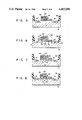
- FIG. 1 shows a cross sectional view of an embodiment of a semiconductor memory element according to the invention
- FIG. 2 shows an equivalent circuit of the memory element shown in FIG. 1;
- FIG. 3 shows a plan view of the memory element shown in FIG. 1;
- FIGS. 4 and 5 show cross sectional views of the memory elements of other embodiments of the invention, which are depicted in a similar way to that in FIG. 1;
- FIG. 6 shows a cross sectional view of the memory element as another embodiment of the invention.
- FIGS. 7 and 8 show cross sectional views of the memory elements as other embodiments of the invention, which are displayed in a similar way to that in FIG. 6;
- FIG. 9 shows a circuit diagram of a memory circuit having a plurality of the above-mentioned type memory elements as an embodiment of the invention.
- FIGS. 10A to 10E show a set of timing charts of various voltage signals applied useful in explaining a data write operation by the memory circuit shown in FIG. 9;
- FIGS. 11A to 11F show a set of timing charts of various voltage signals applied useful in explaining another data write operation by the memory circuit in FIG. 9.
- reference numeral 12 designates a semiconductor substrate of P conductivity type, for example, which is made of silicon.
- source and drain regions 14 and 16 having high impurity concentration are embedded with a suitable interval therebetween as shown.
- the conductivity of the source and drain regions 14 and 16 is of N type which is opposite to that (P type) of the substrate 12.
- a floating gate electrode 22 as a first gate electrode is partially formed, being self-aligned with the source region 14, with a silicon oxide film (SiO 2 ) 20 as a first gate insulation layer which is layered between the major surface and the floating gate electrode 22.
- the floating gate electrode 22 may be made of polycrystalline silicon (poli-silicon) and may be prepared by the chemical vapor deposition (CVD) process, for example.
- a control gate electrode 26 as a second gate electrode is layered on the floating gate electrode 22 with an interposition therebetween of a second gate insulation layer 24 preferably having the same construction as that of the first insulation layer 20.
- An addressing gate electrode 30 as a third gate electrode is layered over a third gate insulation layer 28 preferably having the same construction as that of the first or second gate insulation layer, which also is layered over the control gate electrode 26.
- the addressing gate electrode 30 includes an extension 34 (e.g. 3 ⁇ m) extending over the portion of the first insulation layer 20 which is located on the channel region 18 not covered by the floating gate electrode 22 and the control gate electrode 26.
- a field insulation film 36 is formed on the field region of the substrate 12.
- the floating gate electrode 22, the control gate electrode 26 and the addressing gate electrode 30 may be made of impurity doped poly-silicon.
- the addressing gate electrode 30 may be made of aluminium (Al), refractory metal or metal silicide.
- FIG. 2 shows an equivalent circuit of the memory element shown in FIG. 1.
- a DC voltage V CG +25 V, for example, is applied in advance of applying data writing signals to the control gate 26.
- a drain pulse voltage V D of about 10 V and an addressing pulse voltage V AG of about 10 V are applied as the data writing signals to the drain region 16 and the addressing gate electrode 30 respectively. Since the voltage V CG of about +25 V is applied in advance of applying the data writing signals to the control gate 26, and the extension 34 of the addressing gate 30 is disposed closer to the substrate 12, the addressing pulse voltage V AG at the time of the data write may be low, for example, about +10 V.
- the drain voltage V D may also be low, +10 V, for example.
- the memory element shown in FIG. 1 operates in the saturation region with such low voltages V AG and V D , to form an N channel ranging from the source region 14 to the drain region 16.
- the electrons moving through the N channel causes an impact ionization in the N channel due to a high electric field in the channel to thereby produce hot electrons of high energy. Part of those hot electrons are injected into the gate insulation layers 20, 24 and 28. During the moving, the electrons are trapped by the floating gate provided between the substrate 112 and the control gate electrode 26. Data is written into the memory element in this way.
- the addressing pulse voltage V AG is applied to the addressing gate 30 to form a channel in the substrate 12 under the extension 34 of the addressing gate electrode 30 thus to have the knowledge on the conduction or non-conduction state between the source region 14 and the drain region 16.
- positive or negative high voltage about 50 (V), for example, is applied to the control gate electrode 26 to remove the electrons due to a tunnel emission of Fowler-Nordheim type.
- the voltage V CG of about + ⁇ V is applied to the control gate electrode 26 in the data write and the effective length of the channel is reduced. Therefore, the writing speed of the memory may be improved up to within 500 ⁇ s. Further, the memory element of the invention allows the use of low voltage for the addressing pulse voltage V AG and the drain voltage V D at the time of the data write. For this, the integration density of the memory circuit having a plurality of the memory elements and the integration density of its peripheral circuits can be improved. Further, in the data write, the voltage V CG is applied in advance of applying the data writing signals to the control gate electrode 26.
- the floating gate electrode 22 greatly extending over the field region to gain a large capacitance, unlike the conventional memory element. Accordingly, the floating gate electrode 22 merely extends to the field region by a slight amount of distance, as shown in FIG. 3. Also in this point, the memory element is suitable for high density integration.
- FIGS. 4 and 5 show other embodiments of the memory elements according to the invention. Those embodiments are basically the same as that in FIG. 1 and accordingly, like numerals are used to designate like portions in FIG. 1. Only the different portions from the FIG. 1 embodiment will be described.
- the floating gate electrode 42 is not self-aligned with the source region. In other words, the floating gate electrode 42 does not extend to the side edge of the source region 14 closer to the drain region 16.
- An extension of the control gate electrode 44 extending over the first insulation layer 20 intervenes between the floating gate electrode 42 and the source region 14. The extension of the control gate 44 is self-aligned with the source region 14.
- control gate electrode 52 does not cover the entire of the floating gate electrode 54. That is, the control gate electrode 54 is absent at a portion of the floating gate electrode 54 closer to the drain region 16.
- the addressing gate electrode 56 extends over the control-gate-electrode absent portion of the floating gate electrode 54.
- FIGS. 4 and 5 may attain the same effects as those attained by the FIG. 1 embodiment.
- FIG. 6 there is shown another embodiment of the memory element of the invention.
- the feature of the embodiment resides in the use of an N - region 62 with a low impurity concentration in the surface area of the substrate 12, corresponding to the extension 34 of the addressing gate electrode 30 in FIG. 1.
- the N - region 62 is of the same conductivity type as that of the source and drain regions 14 and 16.
- the N - region 62 may be prepared by the ion injection method, the thermal diffusion method using the ion implantation, gas or solid diffusion source, or the combination of those methods.
- the provision of the N - region 62 facilitates the formation of an N channel and makes the channel current path closer to the surface. For this, carriers move through a portion of the N channel in the vicinity of the major surface of the substrate, so that carriers may effectively be injected into the gate insulation layers and trapped by the floating gate electrode 20. This feature further shortens the write time.
- FIGS. 7 and 8 other embodiments of the memory element according to the invention are shown.
- the features of these embodiments reside in that the N - regions 72 and 74 are formed in the surface areas of the substrate 12 under the extensions of the control gate electrode and the addressing gate electrode in the embodiments in FIGS. 4 and 5, as in the embodiment in FIG. 6.
- the N - regions 72 and 74 are the same conductivity type as that of the source 14 and drain 16 and have lower impurity concentration. Those embodiments can attain the shortening of the write time, satisfactorily.
- FIG. 9 shows a memory circuit having a plurality of memory elements as mentioned above arranged in a matrix fashion, which is an embodiment of the invention.
- the control gates of these memory elements 92 1 to 92 4 are commonly connected to one another, and have a DC voltage V CG of +25 V, for example, during memory writing.
- the address gate electrodes of the memory elements 92 1 to 92 2 arranged on a column of the memory matrix are connected commonly to a first column line 94 1 coupled with a pulse voltage V AG1 for addressing.
- the addressing gate electrodes of the memory elements 92 3 and 92 4 arranged on another column are commonly connected to a second column line 94 2 coupled with an address pulse voltage V AG2 .
- the drains of the memory elements 92 1 and 92 3 arranged on a row of the matrix are connected commonly to a first row line 96 1 coupled with a pulse drain voltage V D1 of about 10 V for memory writing.
- the drains of the memory elements 92 2 and 92 4 arranged on another row are commonly connected to a second row line 96 2 of a pulse drain voltage V D2 of about 10 V for memory writing.
- a desired address is specified by selecting the corresponding column and row lines and data is written into or read out from the address specified.
- FIGS. 10A to 10E show wave forms at the respective portions of the memory circuit shown in FIG. 9 in the write mode.
- a period T1 is a write period for the memory element 92 1
- a period T2 is a write period for the memory element 92 4 .
- the gate voltage V CG of +25 V as shown in FIG. 10A is applied to the control gates of the memory elements 92 1 to 92 4 .
- the pulse drain voltage V D1 as shown in FIG. 10B of about 10 V is then applied to the row line 96 1 at a given timing.
- the addressing pulse V AG1 of about 10 V as shown in FIG. 10D is applied to the first column line 94 1 .
- the memory element 92 1 is specified, which is located at the cross point of the row and column lines 96 1 and 94 1 .
- data is written into the specified memory.
- the addressing pulse voltage V AG1 and the drain pulse voltage V D2 as shown in FIGS. 10C and 10E are applied to the column line 94 2 and the row line 96 2 , respectively.
- the addressing pulse voltage V AG (V AG1 , V AG2 , . . . ) applied to the column line 94 (94 1 , 94 2 , . . . ) rises later than the pulse V D (V D1 , V D2 , . . . ) applied to the row line 96 (96 1 , 96 2 , . . . ) and falls earlier than the latter.
- FIGS. 11A to 11F illustrate another write operation different from that shown in FIGS. 10A to 10E.
- the major difference of this data write method resides in that a reverse bias voltage V SUB of about -3 V as shown in FIG. 11A is applied between the substrate 12 and the source region 14. This feature prevents punch-through from occurring in the memory element, improves the density of integration, shortens the write time, and prevents the erroneous data write.
Abstract
Disclosed is a semiconductor memory element having a semiconductor substrate of P conductivity type, source and drain regions which are of N conductivity type and formed in the substrate, a first gate insulation layer formed on the major surface of the substrate, corresponding to a channel region located between the source and drain, a floating gate electrode formed on the first gate insulation layer so as to partially overlap the channel region, a second gate insulation layer formed on the floating gate electrode, a control gate electrode formed on the second gate insulation layer so as to partially overlap the floating gate electrode, and an addressing gate electrode formed on the control gate electrode, extending to a portion of the channel region not covered by the floating gate electrode and the control gate electrode.
Description
This is a continuation of application Ser. No. 103,375, filed Dec. 13, 1979.
This invention relates to a semiconductor memory element of MOS type of which the contents may be electrically rewritten and, more particularly, to a memory circuit having the memory elements arranged in a matrix fashion.
The MOS type memory allowing the rewrite of the contents thereof has well been known and has the following construction. Source and drain regions are formed in a semiconductor substrate of P conductivity type. A first electrode as a floating gate electrode is formed on a channel region between the source and the drain region with a first insulation layer interposed between the first electrode and the channel region. A second gate electrode as a control gate is further formed on the first gate electrode with a second insulation layer interposed between both.
In the write operation, a positive voltage (20 V or more) is applied to the control gate electrode while at the same time a positive voltage is applied to the drain. The transistor operates in a saturation region. Under this condition, an N-channel is formed between the source and the drain. High energy potential electrons arising from inpact ionization in the N-channel region are injected into the first and second insulation layers and attracted toward the control gate electrode with the positive voltage impressed. At this time, the electrons are trapped by the floating gate electrode so that the N-channel disappears and the MOS transistor is turned off. The write operation is carried out as described above.
In the conventional MOS transistor as a memory element, the read operation is at relatively high speed, but the write operation is at low speed, that is to say, it takes a relatively long time, about 2 ms. Further, the voltages applied to the drain and the control gate in the write operation is high, e.g. 20 V or more. This is disadvantageous in fabricating the memory device having the memory elements of this type with high density and large memory capacity.
In the conventional memory element, in order to improve the efficiency of the electron injection into the floating gate, the floating gate electrode is greatly extended into the field region so that a capacitance between the control gate and the floating gate can be larger than that between the floating gate and the substrate and the electric field in the first insulation layer becomes large enough to increase the electron injection. This results in a bulky memory element and therefore is disadvantageous in fabricating the integrated circuit with high density.
Accordingly, an object of the invention is to provide a semiconductor memory element of MOS type with a decreased write voltage and shortened write time.
Another object of the invention is to provide a memory circuit having the MOS memory elements which effects the write operation at decreased voltage and for shortened time.
According to one aspect of the invention, there is provided a semiconductor memory element comprising: a semiconductor substrate of a first conductivity type; source and drain regions which are formed in the semiconductor substrate and are of a second conductivity type opposite to that of the first conductivity; a first gate insulation layer formed on the major surface of the substrate, corresponding to a channel region between the source and the drain; a first gate electrode formed on the first gate insulation layer so as to partially overlap the channel region; a second gate insulation layer formed on the first gate electrode; a second gate electrode formed on the second gate insulation layer so as to partially overlap the first gate electrode; a third gate insulation layer formed on the second gate electrode; and a third gate electrode formed on the third gate insulation layer, extending to a portion of the channel region not covered by the first and second gate electrodes.
According to another aspect of the invention, there is provided a semiconductor circuit having a plurality of memory elements in a matrix fashion, each memory element including a semiconductor substrate of a first conductivity type, source and drain regions which are formed in the semiconductor substrate and are of a second conductivity type opposite to that of the first conductivity, a first gate insulation layer formed on the major surface of the substrate, corresponding to a channel region between the source and the drain, a first gate electrode formed on the first gate insulation layer so as to partially overlap the channel region, a second gate insulation layer formed in the first gate electrode, a second gate electrode formed on the second gate insulation layer so as to partially overlap the first gate electrode, a third gate insulation layer formed on the second gate electrode, and a third gate electrode formed on the third gate insulation layer, extending to a portion of the channel region not covered by the first and second gate electrodes, wherein the second gate electrodes of the semiconductor memory elements are commonly connected to one another, the drain regions of the memory elements arranged on a row of the matrix are commonly connected one another, the third gate electrodes of the memory elements arranged on a column are commonly connected one another.
According to yet another aspect of the invention, there is provided an operation method used in the memory circuit mentioned above comprising a step for applying, in advance of applying data writing signals, a fixed voltage to the second gate electrode of each memory element in the write mode for writing data into the respective memory elements; and a step for applying pulse voltages as the data writing signals to the drain region and the third gate electrode of the memory element, respectively, to be selected at a write timing.
Other objects and features of the invention will be apparent from the following description taken in connection with the accompanying drawings, in which:
FIG. 1 shows a cross sectional view of an embodiment of a semiconductor memory element according to the invention;
FIG. 2 shows an equivalent circuit of the memory element shown in FIG. 1;
FIG. 3 shows a plan view of the memory element shown in FIG. 1;
FIGS. 4 and 5 show cross sectional views of the memory elements of other embodiments of the invention, which are depicted in a similar way to that in FIG. 1;
FIG. 6 shows a cross sectional view of the memory element as another embodiment of the invention;
FIGS. 7 and 8 show cross sectional views of the memory elements as other embodiments of the invention, which are displayed in a similar way to that in FIG. 6;
FIG. 9 shows a circuit diagram of a memory circuit having a plurality of the above-mentioned type memory elements as an embodiment of the invention;
FIGS. 10A to 10E show a set of timing charts of various voltage signals applied useful in explaining a data write operation by the memory circuit shown in FIG. 9; and
FIGS. 11A to 11F show a set of timing charts of various voltage signals applied useful in explaining another data write operation by the memory circuit in FIG. 9.
Referring now to FIG. 1, there is shown an embodiment of a MOS type semiconductor memory element according to the invention. In the figure, reference numeral 12 designates a semiconductor substrate of P conductivity type, for example, which is made of silicon. In the semiconductor substrate 12, source and drain regions 14 and 16 having high impurity concentration are embedded with a suitable interval therebetween as shown. The conductivity of the source and drain regions 14 and 16 is of N type which is opposite to that (P type) of the substrate 12. On the major surface of the substrate 12, located at an N channel region 18 between the source and drain regions 14 and 16, a floating gate electrode 22 as a first gate electrode is partially formed, being self-aligned with the source region 14, with a silicon oxide film (SiO2) 20 as a first gate insulation layer which is layered between the major surface and the floating gate electrode 22. The floating gate electrode 22 may be made of polycrystalline silicon (poli-silicon) and may be prepared by the chemical vapor deposition (CVD) process, for example. A control gate electrode 26 as a second gate electrode is layered on the floating gate electrode 22 with an interposition therebetween of a second gate insulation layer 24 preferably having the same construction as that of the first insulation layer 20. An addressing gate electrode 30 as a third gate electrode is layered over a third gate insulation layer 28 preferably having the same construction as that of the first or second gate insulation layer, which also is layered over the control gate electrode 26. The addressing gate electrode 30 includes an extension 34 (e.g. 3 μm) extending over the portion of the first insulation layer 20 which is located on the channel region 18 not covered by the floating gate electrode 22 and the control gate electrode 26. A field insulation film 36 is formed on the field region of the substrate 12.
The floating gate electrode 22, the control gate electrode 26 and the addressing gate electrode 30 may be made of impurity doped poly-silicon. Particularly, the addressing gate electrode 30 may be made of aluminium (Al), refractory metal or metal silicide.
FIG. 2 shows an equivalent circuit of the memory element shown in FIG. 1.
In the data write operation, a DC voltage VCG, +25 V, for example, is applied in advance of applying data writing signals to the control gate 26. At the data write, a drain pulse voltage VD of about 10 V and an addressing pulse voltage VAG of about 10 V are applied as the data writing signals to the drain region 16 and the addressing gate electrode 30 respectively. Since the voltage VCG of about +25 V is applied in advance of applying the data writing signals to the control gate 26, and the extension 34 of the addressing gate 30 is disposed closer to the substrate 12, the addressing pulse voltage VAG at the time of the data write may be low, for example, about +10 V. Further, since the effective channel length is reduced to the length of the portion 32 corresponding to the extension 34 of the addressing electrode 30, the drain voltage VD may also be low, +10 V, for example. The memory element shown in FIG. 1 operates in the saturation region with such low voltages VAG and VD, to form an N channel ranging from the source region 14 to the drain region 16. The electrons moving through the N channel causes an impact ionization in the N channel due to a high electric field in the channel to thereby produce hot electrons of high energy. Part of those hot electrons are injected into the gate insulation layers 20, 24 and 28. During the moving, the electrons are trapped by the floating gate provided between the substrate 112 and the control gate electrode 26. Data is written into the memory element in this way. In data read operation, the addressing pulse voltage VAG is applied to the addressing gate 30 to form a channel in the substrate 12 under the extension 34 of the addressing gate electrode 30 thus to have the knowledge on the conduction or non-conduction state between the source region 14 and the drain region 16.
For the erasure of the stored data, positive or negative high voltage, about 50 (V), for example, is applied to the control gate electrode 26 to remove the electrons due to a tunnel emission of Fowler-Nordheim type.
In the memory element of FIG. 1, in advance of applying data writing signals, the voltage VCG of about +≅V is applied to the control gate electrode 26 in the data write and the effective length of the channel is reduced. Therefore, the writing speed of the memory may be improved up to within 500 μs. Further, the memory element of the invention allows the use of low voltage for the addressing pulse voltage VAG and the drain voltage VD at the time of the data write. For this, the integration density of the memory circuit having a plurality of the memory elements and the integration density of its peripheral circuits can be improved. Further, in the data write, the voltage VCG is applied in advance of applying the data writing signals to the control gate electrode 26. This feature eliminates the large floating gate electrode 22 greatly extending over the field region to gain a large capacitance, unlike the conventional memory element. Accordingly, the floating gate electrode 22 merely extends to the field region by a slight amount of distance, as shown in FIG. 3. Also in this point, the memory element is suitable for high density integration.
FIGS. 4 and 5 show other embodiments of the memory elements according to the invention. Those embodiments are basically the same as that in FIG. 1 and accordingly, like numerals are used to designate like portions in FIG. 1. Only the different portions from the FIG. 1 embodiment will be described.
In the embodiment in FIG. 4, the floating gate electrode 42 is not self-aligned with the source region. In other words, the floating gate electrode 42 does not extend to the side edge of the source region 14 closer to the drain region 16. An extension of the control gate electrode 44 extending over the first insulation layer 20 intervenes between the floating gate electrode 42 and the source region 14. The extension of the control gate 44 is self-aligned with the source region 14.
In the embodiment in FIG. 5 having the same construction as that of the FIG. 4 embodiment, the control gate electrode 52 does not cover the entire of the floating gate electrode 54. That is, the control gate electrode 54 is absent at a portion of the floating gate electrode 54 closer to the drain region 16. The addressing gate electrode 56 extends over the control-gate-electrode absent portion of the floating gate electrode 54.
Those embodiments in FIGS. 4 and 5 may attain the same effects as those attained by the FIG. 1 embodiment.
Turning now to FIG. 6, there is shown another embodiment of the memory element of the invention. The feature of the embodiment resides in the use of an N- region 62 with a low impurity concentration in the surface area of the substrate 12, corresponding to the extension 34 of the addressing gate electrode 30 in FIG. 1. The N- region 62 is of the same conductivity type as that of the source and drain regions 14 and 16. The N- region 62 may be prepared by the ion injection method, the thermal diffusion method using the ion implantation, gas or solid diffusion source, or the combination of those methods.
The provision of the N- region 62 facilitates the formation of an N channel and makes the channel current path closer to the surface. For this, carriers move through a portion of the N channel in the vicinity of the major surface of the substrate, so that carriers may effectively be injected into the gate insulation layers and trapped by the floating gate electrode 20. This feature further shortens the write time.
Turning now to FIGS. 7 and 8, other embodiments of the memory element according to the invention are shown. The features of these embodiments reside in that the N- regions 72 and 74 are formed in the surface areas of the substrate 12 under the extensions of the control gate electrode and the addressing gate electrode in the embodiments in FIGS. 4 and 5, as in the embodiment in FIG. 6. The N- regions 72 and 74 are the same conductivity type as that of the source 14 and drain 16 and have lower impurity concentration. Those embodiments can attain the shortening of the write time, satisfactorily.
FIG. 9 shows a memory circuit having a plurality of memory elements as mentioned above arranged in a matrix fashion, which is an embodiment of the invention. In the embodiment, only four memory elements 921 to 924 are used for simplicity. The control gates of these memory elements 921 to 924 are commonly connected to one another, and have a DC voltage VCG of +25 V, for example, during memory writing. The address gate electrodes of the memory elements 921 to 922 arranged on a column of the memory matrix are connected commonly to a first column line 941 coupled with a pulse voltage VAG1 for addressing. Similarly, the addressing gate electrodes of the memory elements 923 and 924 arranged on another column are commonly connected to a second column line 942 coupled with an address pulse voltage VAG2. The drains of the memory elements 921 and 923 arranged on a row of the matrix are connected commonly to a first row line 961 coupled with a pulse drain voltage VD1 of about 10 V for memory writing. Similarly, the drains of the memory elements 922 and 924 arranged on another row are commonly connected to a second row line 962 of a pulse drain voltage VD2 of about 10 V for memory writing.
In operation, a desired address is specified by selecting the corresponding column and row lines and data is written into or read out from the address specified.
FIGS. 10A to 10E show wave forms at the respective portions of the memory circuit shown in FIG. 9 in the write mode. In those figures, a period T1 is a write period for the memory element 921 and a period T2 is a write period for the memory element 924. There will now be described how to write data into the memory element 924. Before data is written into the respective memories 921 to 924, the gate voltage VCG of +25 V as shown in FIG. 10A is applied to the control gates of the memory elements 921 to 924. In writing data into the memory element 921, the pulse drain voltage VD1 as shown in FIG. 10B of about 10 V is then applied to the row line 961 at a given timing. Within the duration of the drain pulse voltage VD1, the addressing pulse VAG1 of about 10 V as shown in FIG. 10D is applied to the first column line 941. As a result, the memory element 921 is specified, which is located at the cross point of the row and column lines 961 and 941. Then, data is written into the specified memory. For writing data into the memory element 924, the addressing pulse voltage VAG1 and the drain pulse voltage VD2 as shown in FIGS. 10C and 10E are applied to the column line 942 and the row line 962, respectively.
In order to prevent an erroneous data write, it is preferable that the addressing pulse voltage VAG (VAG1, VAG2, . . . ) applied to the column line 94 (941, 942, . . . ) rises later than the pulse VD (VD1, VD2, . . . ) applied to the row line 96 (961, 962, . . . ) and falls earlier than the latter.
FIGS. 11A to 11F illustrate another write operation different from that shown in FIGS. 10A to 10E. The major difference of this data write method resides in that a reverse bias voltage VSUB of about -3 V as shown in FIG. 11A is applied between the substrate 12 and the source region 14. This feature prevents punch-through from occurring in the memory element, improves the density of integration, shortens the write time, and prevents the erroneous data write.
Claims (2)
1. A method of operating a semiconductor memory circuit comprising: a plurality of memory elements in a matrix fashion with each memory element including a semiconductor substrate of a first conductivity type, source and drain regions which are formed in the semiconductor substrate and are of a second conductivity type opposite to that of said first conductivity, a first gate insulation layer formed on the major surface of said substrate, corresponding to a channel region between said source and drain, a first gate electrode acting as a floating gate electrode formed on said first gate insulation layer, the first gate electrode located nearer said source region than said drain region, a second gate insulation layer formed on said first gate electrode, a second gate electrode acting as a control gate electrode formed on said second gate insulation layer so as to partially overlap said first gate electrode, a third gate insulation layer formed on said second gate electrode, and a third gate electrode acting as an addressing gate electrode formed on said third gate insulation layer, extending to a portion of said channel region not covered by said first and second electrodes, wherein said second gate electrodes of said semiconductor memory elements are commonly connected to one another, the drain regions of said memory elements arranged on a row/column of said matrix are commonly connected to one another, said third gate electrodes of said memory elements arranged on a column/row are commonly connected to one another including the steps of:
applying, in advance of applying data write signals, a fixed voltage to said second gate electrode of each of said memory elements in the write mode for writing data into said respective memory elements; and applying pulse voltages as the data writing signals to the drain region and said third gate electrodes of the memory element, respectively, to be selected at a write timing.
2. The method of claim 1 further including the step of;
applying a positive or negative high voltage to said second gate electrode of said each memory element in the erasing mode for erasing the data stored.
Applications Claiming Priority (2)
| Application Number | Priority Date | Filing Date | Title |
|---|---|---|---|
| JP53153741A JPS6046554B2 (en) | 1978-12-14 | 1978-12-14 | Semiconductor memory elements and memory circuits |
| JP53-153741 | 1978-12-14 |
Related Parent Applications (1)
| Application Number | Title | Priority Date | Filing Date |
|---|---|---|---|
| US06103375 Continuation | 1979-12-13 |
Publications (1)
| Publication Number | Publication Date |
|---|---|
| US4462090A true US4462090A (en) | 1984-07-24 |
Family
ID=15569085
Family Applications (1)
| Application Number | Title | Priority Date | Filing Date |
|---|---|---|---|
| US06/393,608 Expired - Lifetime US4462090A (en) | 1978-12-14 | 1982-06-30 | Method of operating a semiconductor memory circuit |
Country Status (2)
| Country | Link |
|---|---|
| US (1) | US4462090A (en) |
| JP (1) | JPS6046554B2 (en) |
Cited By (81)
| Publication number | Priority date | Publication date | Assignee | Title |
|---|---|---|---|---|
| US4536785A (en) * | 1983-08-26 | 1985-08-20 | Gibbons James F | One transistor dynamic random access memory |
| US4652897A (en) * | 1984-07-13 | 1987-03-24 | Hitachi, Ltd. | Semiconductor memory device |
| US4663645A (en) * | 1984-05-23 | 1987-05-05 | Hitachi, Ltd. | Semiconductor device of an LDD structure having a floating gate |
| US4754320A (en) * | 1985-02-25 | 1988-06-28 | Kabushiki Kaisha Toshiba | EEPROM with sidewall control gate |
| US4769788A (en) * | 1986-09-22 | 1988-09-06 | Ncr Corporation | Shared line direct write nonvolatile memory cell array |
| EP0284724A2 (en) * | 1987-01-31 | 1988-10-05 | Kabushiki Kaisha Toshiba | Nonvolatile semiconductor memory device |
| US4795719A (en) * | 1984-05-15 | 1989-01-03 | Waferscale Integration, Inc. | Self-aligned split gate eprom process |
| US4821236A (en) * | 1983-03-07 | 1989-04-11 | Kogyo Gizyutsuin | Semiconductor nonvolatile memory |
| US4852062A (en) * | 1987-09-28 | 1989-07-25 | Motorola, Inc. | EPROM device using asymmetrical transistor characteristics |
| US4861730A (en) * | 1988-01-25 | 1989-08-29 | Catalyst Semiconductor, Inc. | Process for making a high density split gate nonvolatile memory cell |
| US4868629A (en) * | 1984-05-15 | 1989-09-19 | Waferscale Integration, Inc. | Self-aligned split gate EPROM |
| US4870470A (en) * | 1987-10-16 | 1989-09-26 | International Business Machines Corporation | Non-volatile memory cell having Si rich silicon nitride charge trapping layer |
| EP0335395A2 (en) * | 1988-03-30 | 1989-10-04 | Kabushiki Kaisha Toshiba | Non-volatile semiconductor memory device and method for manufacture thereof |
| EP0370416A2 (en) * | 1988-11-23 | 1990-05-30 | National Semiconductor Corporation | Novel architecture for a flash erase EPROM memory |
| US4939558A (en) * | 1985-09-27 | 1990-07-03 | Texas Instruments Incorporated | EEPROM memory cell and driving circuitry |
| US4947222A (en) * | 1988-07-15 | 1990-08-07 | Texas Instruments Incorporated | Electrically programmable and erasable memory cells with field plate conductor defined drain regions |
| WO1990016085A1 (en) * | 1989-06-21 | 1990-12-27 | Xicor, Inc. | Apparatus and method for a dual thickness dielectric floating gate memory cell |
| US4988635A (en) * | 1988-06-07 | 1991-01-29 | Mitsubishi Denki Kabushiki Kaisha | Method of manufacturing non-volatile semiconductor memory device |
| EP0411573A2 (en) * | 1989-07-31 | 1991-02-06 | Kabushiki Kaisha Toshiba | Nonvolatile semiconductor memory device and method of operating the same |
| US5021847A (en) * | 1984-05-15 | 1991-06-04 | Waferscale Integration, Inc. | Split gate memory array having staggered floating gate rows and method for making same |
| US5073513A (en) * | 1989-08-17 | 1991-12-17 | Samsung Electronics Co., Ltd. | Manufacture of a nonvolatile semiconductor memory device having a sidewall select gate |
| US5084745A (en) * | 1983-04-18 | 1992-01-28 | Kabushiki Kaisha Toshiba | Semiconductor memory device having a floating gate |
| EP0468218A1 (en) * | 1990-06-26 | 1992-01-29 | Sharp Kabushiki Kaisha | Semiconductor memory device |
| US5095344A (en) * | 1988-06-08 | 1992-03-10 | Eliyahou Harari | Highly compact eprom and flash eeprom devices |
| US5153691A (en) * | 1989-06-21 | 1992-10-06 | Xicor, Inc. | Apparatus for a dual thickness floating gate memory cell |
| US5153684A (en) * | 1988-10-19 | 1992-10-06 | Kabushiki Kaisha Toshiba | Nonvolatile semiconductor memory device with offset transistor |
| EP0509698A2 (en) * | 1991-04-18 | 1992-10-21 | National Semiconductor Corporation | Contactless EPROM array |
| US5168465A (en) * | 1988-06-08 | 1992-12-01 | Eliyahou Harari | Highly compact EPROM and flash EEPROM devices |
| US5216269A (en) * | 1989-03-31 | 1993-06-01 | U.S. Philips Corp. | Electrically-programmable semiconductor memories with buried injector region |
| US5241205A (en) * | 1990-06-26 | 1993-08-31 | Sharp Kabushiki Kaisha | Semiconductor memory device |
| US5243210A (en) * | 1987-02-21 | 1993-09-07 | Kabushiki Kaisha Toshiba | Semiconductor memory device and manufacturing method thereof |
| US5280446A (en) * | 1990-09-20 | 1994-01-18 | Bright Microelectronics, Inc. | Flash eprom memory circuit having source side programming |
| US5291439A (en) * | 1991-09-12 | 1994-03-01 | International Business Machines Corporation | Semiconductor memory cell and memory array with inversion layer |
| US5313421A (en) * | 1992-01-14 | 1994-05-17 | Sundisk Corporation | EEPROM with split gate source side injection |
| US5352620A (en) * | 1984-05-23 | 1994-10-04 | Hitachi, Ltd. | Method of making semiconductor device with memory cells and peripheral transistors |
| US5592001A (en) * | 1990-06-22 | 1997-01-07 | Kabushiki Kaisha Toshiba | Non-volatile semiconductor memory device |
| US5668757A (en) * | 1996-03-18 | 1997-09-16 | Jeng; Ching-Shi | Scalable flash eeprom memory cell and array |
| US5691939A (en) * | 1995-12-07 | 1997-11-25 | Programmable Microelectronics Corporation | Triple poly PMOS flash memory cell |
| US5712180A (en) * | 1992-01-14 | 1998-01-27 | Sundisk Corporation | EEPROM with split gate source side injection |
| US5719520A (en) * | 1994-02-15 | 1998-02-17 | Tadashi Shibata | Multi-valued ROM circuit #7 |
| US5856983A (en) * | 1996-06-27 | 1999-01-05 | Kabushiki Kaisha Toshiba | Magnetic disk drive and error correction method |
| US5856943A (en) * | 1996-03-18 | 1999-01-05 | Integrated Memory Technologies, Inc. | Scalable flash EEPROM memory cell and array |
| EP0902438A1 (en) * | 1997-09-09 | 1999-03-17 | Interuniversitair Micro-Elektronica Centrum Vzw | Methods of erasing a memory device and a method of programming a memory device for low-voltage and low-power applications |
| US5912843A (en) * | 1996-03-18 | 1999-06-15 | Integrated Memory Technologies, Inc. | Scalable flash EEPROM memory cell, method of manufacturing and operation thereof |
| US6057575A (en) * | 1996-03-18 | 2000-05-02 | Integrated Memory Technologies, Inc. | Scalable flash EEPROM memory cell, method of manufacturing and operation thereof |
| US6222762B1 (en) | 1992-01-14 | 2001-04-24 | Sandisk Corporation | Multi-state memory |
| EP1089340A3 (en) * | 1999-09-30 | 2001-08-22 | Micronas GmbH | EPROM structure for semiconductor memory |
| GB2364436A (en) * | 1999-12-22 | 2002-01-23 | Hyundai Electronics Ind | Multi-level flash EEPROM cell |
| US6476440B1 (en) * | 1999-08-24 | 2002-11-05 | Hyundai Electronics Industries Co., Inc. | Nonvolatile memory device and method of manufacturing the same |
| EP1089332A3 (en) * | 1999-09-30 | 2003-01-08 | Micronas GmbH | Method for the manufacture of a CMOS-integrated memory |
| US20030052360A1 (en) * | 1992-01-14 | 2003-03-20 | Guterman Daniel C. | EEPROM with split gate source side injection with sidewall spacers |
| US6563733B2 (en) | 2001-05-24 | 2003-05-13 | Winbond Electronics Corporation | Memory array architectures based on a triple-polysilicon source-side injection non-volatile memory cell |
| US6621115B2 (en) | 2001-11-06 | 2003-09-16 | Integrated Memory Technologies, Inc. | Scalable flash EEPROM memory cell with floating gate spacer wrapped by control gate |
| US20030223288A1 (en) * | 2002-03-19 | 2003-12-04 | O2Ic, Inc. | Non-volatile memory device |
| US20030231528A1 (en) * | 2002-03-19 | 2003-12-18 | 021C, Inc. | Non-volatile differential dynamic random access memory |
| US20030234397A1 (en) * | 2002-03-22 | 2003-12-25 | Gunter Schmid | Semiconductor memory cell and semiconductor memory device |
| US20040016947A1 (en) * | 2002-03-19 | 2004-01-29 | O2Ic, Inc. | Non-volatile dynamic random access memory |
| US6703662B1 (en) * | 1999-12-21 | 2004-03-09 | Nec Electronics Corporation | Semiconductor device and manufacturing method thereof |
| US20050036393A1 (en) * | 2003-07-02 | 2005-02-17 | Ching-Shi Jenq | Scalable flash EEPROM memory cell with notched floating gate and graded source region, and method of manufacturing the same |
| US20050161718A1 (en) * | 2004-01-28 | 2005-07-28 | O2Ic, Inc. | Non-volatile DRAM and a method of making thereof |
| US20050170586A1 (en) * | 2004-01-29 | 2005-08-04 | O2Ic, Inc., (A California Corporation) | Method of manufacturing non-volatile DRAM |
| DE19709926B4 (en) * | 1996-03-11 | 2005-09-08 | Hyundai Electronics Industries Co., Ltd., Ichon | EEPROM flash cell and method of making same |
| US20050201150A1 (en) * | 2003-06-06 | 2005-09-15 | Chih-Hsin Wang | Method and apparatus for semiconductor device and semiconductor memory device |
| US20050219913A1 (en) * | 2004-04-06 | 2005-10-06 | O2Ic, Inc. | Non-volatile memory array |
| US6965524B2 (en) * | 2002-03-19 | 2005-11-15 | O2Ic, Inc. | Non-volatile static random access memory |
| US6972229B2 (en) | 2003-12-23 | 2005-12-06 | 02Ic, Inc. | Method of manufacturing self-aligned non-volatile memory device |
| US20050269622A1 (en) * | 2004-06-07 | 2005-12-08 | Pavel Klinger | Semiconductor memory array of floating gate memory cells with program/erase and select gates, and methods of making and operating same |
| US20060001053A1 (en) * | 2003-06-06 | 2006-01-05 | Chih-Hsin Wang | Method and apparatus transporting charges in semiconductor device and semiconductor memory device |
| US20060007772A1 (en) * | 2002-03-19 | 2006-01-12 | O2Ic, Inc. | Non-volatile memory device |
| US20060006454A1 (en) * | 2004-07-01 | 2006-01-12 | Chih-Hsin Wang | Electrically alterable memory cell |
| US20060193174A1 (en) * | 2005-02-25 | 2006-08-31 | O2Ic | Non-volatile and static random access memory cells sharing the same bitlines |
| US20060289924A1 (en) * | 2005-06-28 | 2006-12-28 | Chih-Hsin Wang | Low power electrically alterable nonvolatile memory cells and arrays |
| US20070008778A1 (en) * | 2003-06-06 | 2007-01-11 | Chih-Hsin Wang | Methods for operating semiconductor device and semiconductor memory device |
| US7232717B1 (en) | 2002-05-28 | 2007-06-19 | O2Ic, Inc. | Method of manufacturing non-volatile DRAM |
| US20070242514A1 (en) * | 2005-03-10 | 2007-10-18 | O2Ic, Inc. | NAND-structured nonvolatile memory cell |
| US20080203464A1 (en) * | 2004-07-01 | 2008-08-28 | Chih-Hsin Wang | Electrically alterable non-volatile memory and array |
| US20080283825A1 (en) * | 2004-04-05 | 2008-11-20 | Lay-Lay Chua | Dual-Gate Transistors |
| US20110140189A1 (en) * | 2009-12-10 | 2011-06-16 | Electronics And Telecommunications Research Institute | Electrically erasable programmable read-only memory and manufacturing method thereof |
| US8072023B1 (en) | 2007-11-12 | 2011-12-06 | Marvell International Ltd. | Isolation for non-volatile memory cell array |
| US8120088B1 (en) | 2007-12-07 | 2012-02-21 | Marvell International Ltd. | Non-volatile memory cell and array |
| US8320191B2 (en) | 2007-08-30 | 2012-11-27 | Infineon Technologies Ag | Memory cell arrangement, method for controlling a memory cell, memory array and electronic device |
Families Citing this family (4)
| Publication number | Priority date | Publication date | Assignee | Title |
|---|---|---|---|---|
| JPH07112018B2 (en) * | 1984-03-31 | 1995-11-29 | 株式会社東芝 | Semiconductor memory device |
| US4688243A (en) * | 1985-08-21 | 1987-08-18 | E. I. Du Pont De Nemours And Company | Daylight X-ray cassette having variable size leaf springs |
| BRPI0621526A2 (en) | 2006-03-31 | 2011-12-13 | Maspro Denko Kk | coaxial cable connector |
| JP2009010281A (en) * | 2007-06-29 | 2009-01-15 | Renesas Technology Corp | Semiconductor device and manufacturing method thereof |
Citations (7)
| Publication number | Priority date | Publication date | Assignee | Title |
|---|---|---|---|---|
| US3728695A (en) * | 1971-10-06 | 1973-04-17 | Intel Corp | Random-access floating gate mos memory array |
| US3825945A (en) * | 1972-02-29 | 1974-07-23 | Tokyo Shibaura Electric Co | Field effect semiconductor memory apparatus with a floating gate |
| US3836992A (en) * | 1973-03-16 | 1974-09-17 | Ibm | Electrically erasable floating gate fet memory cell |
| US4051464A (en) * | 1975-09-08 | 1977-09-27 | Honeywell Inc. | Semiconductor memory cell |
| US4099196A (en) * | 1977-06-29 | 1978-07-04 | Intel Corporation | Triple layer polysilicon cell |
| US4122544A (en) * | 1976-12-27 | 1978-10-24 | Texas Instruments Incorporated | Electrically alterable floating gate semiconductor memory device with series enhancement transistor |
| US4258378A (en) * | 1978-05-26 | 1981-03-24 | Texas Instruments Incorporated | Electrically alterable floating gate memory with self-aligned low-threshold series enhancement transistor |
-
1978
- 1978-12-14 JP JP53153741A patent/JPS6046554B2/en not_active Expired
-
1982
- 1982-06-30 US US06/393,608 patent/US4462090A/en not_active Expired - Lifetime
Patent Citations (7)
| Publication number | Priority date | Publication date | Assignee | Title |
|---|---|---|---|---|
| US3728695A (en) * | 1971-10-06 | 1973-04-17 | Intel Corp | Random-access floating gate mos memory array |
| US3825945A (en) * | 1972-02-29 | 1974-07-23 | Tokyo Shibaura Electric Co | Field effect semiconductor memory apparatus with a floating gate |
| US3836992A (en) * | 1973-03-16 | 1974-09-17 | Ibm | Electrically erasable floating gate fet memory cell |
| US4051464A (en) * | 1975-09-08 | 1977-09-27 | Honeywell Inc. | Semiconductor memory cell |
| US4122544A (en) * | 1976-12-27 | 1978-10-24 | Texas Instruments Incorporated | Electrically alterable floating gate semiconductor memory device with series enhancement transistor |
| US4099196A (en) * | 1977-06-29 | 1978-07-04 | Intel Corporation | Triple layer polysilicon cell |
| US4258378A (en) * | 1978-05-26 | 1981-03-24 | Texas Instruments Incorporated | Electrically alterable floating gate memory with self-aligned low-threshold series enhancement transistor |
Non-Patent Citations (4)
| Title |
|---|
| Das Gupta et al., "Dual-Gate FAMOS Memory Cell", IBM Technical Disclosure Bulletin, vol. 17, (1/75), p. 2266. |
| Das Gupta et al., Dual Gate FAMOS Memory Cell , IBM Technical Disclosure Bulletin, vol. 17, (1/75), p. 2266. * |
| Iizuka et al., "Electrically Alterable Avalanche-Injection-Type MOS Read-Only Memory with Stacked-Gate Structure", IEEE Trans. Electron Devices, vol. ED-23, (4/76), pp. 379-387. |
| Iizuka et al., Electrically Alterable Avalanche Injection Type MOS Read Only Memory with Stacked Gate Structure , IEEE Trans. Electron Devices, vol. ED 23, (4/76), pp. 379 387. * |
Cited By (168)
| Publication number | Priority date | Publication date | Assignee | Title |
|---|---|---|---|---|
| US4821236A (en) * | 1983-03-07 | 1989-04-11 | Kogyo Gizyutsuin | Semiconductor nonvolatile memory |
| US5084745A (en) * | 1983-04-18 | 1992-01-28 | Kabushiki Kaisha Toshiba | Semiconductor memory device having a floating gate |
| US4536785A (en) * | 1983-08-26 | 1985-08-20 | Gibbons James F | One transistor dynamic random access memory |
| US4868629A (en) * | 1984-05-15 | 1989-09-19 | Waferscale Integration, Inc. | Self-aligned split gate EPROM |
| US5021847A (en) * | 1984-05-15 | 1991-06-04 | Waferscale Integration, Inc. | Split gate memory array having staggered floating gate rows and method for making same |
| US4795719A (en) * | 1984-05-15 | 1989-01-03 | Waferscale Integration, Inc. | Self-aligned split gate eprom process |
| US4663645A (en) * | 1984-05-23 | 1987-05-05 | Hitachi, Ltd. | Semiconductor device of an LDD structure having a floating gate |
| US5352620A (en) * | 1984-05-23 | 1994-10-04 | Hitachi, Ltd. | Method of making semiconductor device with memory cells and peripheral transistors |
| US4652897A (en) * | 1984-07-13 | 1987-03-24 | Hitachi, Ltd. | Semiconductor memory device |
| US4754320A (en) * | 1985-02-25 | 1988-06-28 | Kabushiki Kaisha Toshiba | EEPROM with sidewall control gate |
| US4939558A (en) * | 1985-09-27 | 1990-07-03 | Texas Instruments Incorporated | EEPROM memory cell and driving circuitry |
| US4769788A (en) * | 1986-09-22 | 1988-09-06 | Ncr Corporation | Shared line direct write nonvolatile memory cell array |
| US4870615A (en) * | 1987-01-31 | 1989-09-26 | Kabushiki Kaisha Toshiba | Nonvolatile floating gate semiconductor memory device |
| EP0440265A3 (en) * | 1987-01-31 | 1991-08-21 | Kabushiki Kaisha Toshiba | Nonvolatile semiconductor memory device |
| EP0440265A2 (en) * | 1987-01-31 | 1991-08-07 | Kabushiki Kaisha Toshiba | Nonvolatile semiconductor memory device |
| EP0284724A2 (en) * | 1987-01-31 | 1988-10-05 | Kabushiki Kaisha Toshiba | Nonvolatile semiconductor memory device |
| EP0284724A3 (en) * | 1987-01-31 | 1989-03-08 | Kabushiki Kaisha Toshiba | Nonvolatile semiconductor memory device |
| US5243210A (en) * | 1987-02-21 | 1993-09-07 | Kabushiki Kaisha Toshiba | Semiconductor memory device and manufacturing method thereof |
| US4852062A (en) * | 1987-09-28 | 1989-07-25 | Motorola, Inc. | EPROM device using asymmetrical transistor characteristics |
| US4870470A (en) * | 1987-10-16 | 1989-09-26 | International Business Machines Corporation | Non-volatile memory cell having Si rich silicon nitride charge trapping layer |
| US4861730A (en) * | 1988-01-25 | 1989-08-29 | Catalyst Semiconductor, Inc. | Process for making a high density split gate nonvolatile memory cell |
| EP0335395A2 (en) * | 1988-03-30 | 1989-10-04 | Kabushiki Kaisha Toshiba | Non-volatile semiconductor memory device and method for manufacture thereof |
| EP0335395A3 (en) * | 1988-03-30 | 1990-07-25 | Kabushiki Kaisha Toshiba | Non-volatile semiconductor memory device and method for manufacture thereof |
| US4988635A (en) * | 1988-06-07 | 1991-01-29 | Mitsubishi Denki Kabushiki Kaisha | Method of manufacturing non-volatile semiconductor memory device |
| US5095344A (en) * | 1988-06-08 | 1992-03-10 | Eliyahou Harari | Highly compact eprom and flash eeprom devices |
| US5168465A (en) * | 1988-06-08 | 1992-12-01 | Eliyahou Harari | Highly compact EPROM and flash EEPROM devices |
| US4947222A (en) * | 1988-07-15 | 1990-08-07 | Texas Instruments Incorporated | Electrically programmable and erasable memory cells with field plate conductor defined drain regions |
| US5153684A (en) * | 1988-10-19 | 1992-10-06 | Kabushiki Kaisha Toshiba | Nonvolatile semiconductor memory device with offset transistor |
| US4999812A (en) * | 1988-11-23 | 1991-03-12 | National Semiconductor Corp. | Architecture for a flash erase EEPROM memory |
| EP0370416A3 (en) * | 1988-11-23 | 1990-12-05 | National Semiconductor Corporation | Novel architecture for a flash erase eprom memory |
| EP0370416A2 (en) * | 1988-11-23 | 1990-05-30 | National Semiconductor Corporation | Novel architecture for a flash erase EPROM memory |
| US5216269A (en) * | 1989-03-31 | 1993-06-01 | U.S. Philips Corp. | Electrically-programmable semiconductor memories with buried injector region |
| US5153691A (en) * | 1989-06-21 | 1992-10-06 | Xicor, Inc. | Apparatus for a dual thickness floating gate memory cell |
| WO1990016085A1 (en) * | 1989-06-21 | 1990-12-27 | Xicor, Inc. | Apparatus and method for a dual thickness dielectric floating gate memory cell |
| US5091882A (en) * | 1989-07-31 | 1992-02-25 | Kabushiki Kaisha Toshiba | Nonvolatile semiconductor memory device and method of operating the same |
| EP0411573A2 (en) * | 1989-07-31 | 1991-02-06 | Kabushiki Kaisha Toshiba | Nonvolatile semiconductor memory device and method of operating the same |
| EP0411573A3 (en) * | 1989-07-31 | 1991-04-03 | Kabushiki Kaisha Toshiba | Nonvolatile semiconductor memory device and method of operating the same |
| US5073513A (en) * | 1989-08-17 | 1991-12-17 | Samsung Electronics Co., Ltd. | Manufacture of a nonvolatile semiconductor memory device having a sidewall select gate |
| US5592001A (en) * | 1990-06-22 | 1997-01-07 | Kabushiki Kaisha Toshiba | Non-volatile semiconductor memory device |
| US5241205A (en) * | 1990-06-26 | 1993-08-31 | Sharp Kabushiki Kaisha | Semiconductor memory device |
| EP0468218A1 (en) * | 1990-06-26 | 1992-01-29 | Sharp Kabushiki Kaisha | Semiconductor memory device |
| US5280446A (en) * | 1990-09-20 | 1994-01-18 | Bright Microelectronics, Inc. | Flash eprom memory circuit having source side programming |
| WO1995019624A1 (en) * | 1990-09-20 | 1995-07-20 | Bright Microelectronics, Inc. | Flash eprom memory circuit having source side programming |
| EP0509698A3 (en) * | 1991-04-18 | 1993-02-03 | National Semiconductor Corporation | Contactless eprom array |
| EP0509698A2 (en) * | 1991-04-18 | 1992-10-21 | National Semiconductor Corporation | Contactless EPROM array |
| US5291439A (en) * | 1991-09-12 | 1994-03-01 | International Business Machines Corporation | Semiconductor memory cell and memory array with inversion layer |
| US5847996A (en) * | 1992-01-14 | 1998-12-08 | Sandisk Corporation | Eeprom with split gate source side injection |
| US5883409A (en) * | 1992-01-14 | 1999-03-16 | Sandisk Corporation | EEPROM with split gate source side injection |
| US6275419B1 (en) | 1992-01-14 | 2001-08-14 | Sandisk Corporation | Multi-state memory |
| US5712180A (en) * | 1992-01-14 | 1998-01-27 | Sundisk Corporation | EEPROM with split gate source side injection |
| US6856546B2 (en) | 1992-01-14 | 2005-02-15 | Sandisk Corporation | Multi-state memory |
| US5776810A (en) * | 1992-01-14 | 1998-07-07 | Sandisk Corporation | Method for forming EEPROM with split gate source side injection |
| US20030052360A1 (en) * | 1992-01-14 | 2003-03-20 | Guterman Daniel C. | EEPROM with split gate source side injection with sidewall spacers |
| US5313421A (en) * | 1992-01-14 | 1994-05-17 | Sundisk Corporation | EEPROM with split gate source side injection |
| US7898868B2 (en) | 1992-01-14 | 2011-03-01 | Sandisk Corporation | Multi-state memory |
| US6222762B1 (en) | 1992-01-14 | 2001-04-24 | Sandisk Corporation | Multi-state memory |
| US6954381B2 (en) * | 1992-01-14 | 2005-10-11 | Sandisk Corporation | EEPROM with split gate source side injection with sidewall spacers |
| US6317363B1 (en) | 1992-01-14 | 2001-11-13 | Sandisk Corporation | Multi-state memory |
| US5910915A (en) * | 1992-01-14 | 1999-06-08 | Sandisk Corporation | EEPROM with split gate source side injection |
| US5910925A (en) * | 1992-01-14 | 1999-06-08 | Sandisk Corporation | EEPROM with split gate source side injection |
| US6317364B1 (en) | 1992-01-14 | 2001-11-13 | Sandisk Corporation | Multi-state memory |
| US6002152A (en) * | 1992-01-14 | 1999-12-14 | Sandisk Corporation | EEPROM with split gate source side injection with sidewall spacers |
| US5719520A (en) * | 1994-02-15 | 1998-02-17 | Tadashi Shibata | Multi-valued ROM circuit #7 |
| US5691939A (en) * | 1995-12-07 | 1997-11-25 | Programmable Microelectronics Corporation | Triple poly PMOS flash memory cell |
| US20040063283A1 (en) * | 1996-02-28 | 2004-04-01 | Guterman Daniel C. | Eeprom with split gate source side injection |
| US7071060B1 (en) | 1996-02-28 | 2006-07-04 | Sandisk Corporation | EEPROM with split gate source side infection with sidewall spacers |
| US20060163645A1 (en) * | 1996-02-28 | 2006-07-27 | Guterman Daniel C | EEPROM With Split Gate Source Side Injection |
| US7449746B2 (en) | 1996-02-28 | 2008-11-11 | Sandisk Corporation | EEPROM with split gate source side injection |
| US6861700B2 (en) | 1996-02-28 | 2005-03-01 | Sandisk Corporation | Eeprom with split gate source side injection |
| US6704222B2 (en) | 1996-02-28 | 2004-03-09 | Sandisk Corporation | Multi-state operation of dual floating gate array |
| US6664587B2 (en) | 1996-02-28 | 2003-12-16 | Sandisk Corporation | EEPROM cell array structure with specific floating gate shape |
| DE19709926B4 (en) * | 1996-03-11 | 2005-09-08 | Hyundai Electronics Industries Co., Ltd., Ichon | EEPROM flash cell and method of making same |
| US6057575A (en) * | 1996-03-18 | 2000-05-02 | Integrated Memory Technologies, Inc. | Scalable flash EEPROM memory cell, method of manufacturing and operation thereof |
| US5912843A (en) * | 1996-03-18 | 1999-06-15 | Integrated Memory Technologies, Inc. | Scalable flash EEPROM memory cell, method of manufacturing and operation thereof |
| US5856943A (en) * | 1996-03-18 | 1999-01-05 | Integrated Memory Technologies, Inc. | Scalable flash EEPROM memory cell and array |
| US5668757A (en) * | 1996-03-18 | 1997-09-16 | Jeng; Ching-Shi | Scalable flash eeprom memory cell and array |
| US5856983A (en) * | 1996-06-27 | 1999-01-05 | Kabushiki Kaisha Toshiba | Magnetic disk drive and error correction method |
| US7573740B2 (en) | 1997-08-07 | 2009-08-11 | Sandisk Corporation | Multi-state memory |
| US7187592B2 (en) | 1997-08-07 | 2007-03-06 | Sandisk Corporation | Multi-state memory |
| US7443723B2 (en) | 1997-08-07 | 2008-10-28 | Sandisk Corporation | Multi-state memory |
| US20050180211A1 (en) * | 1997-08-07 | 2005-08-18 | Guterman Daniel C. | Novel multi-state memory |
| US20080212374A1 (en) * | 1997-08-07 | 2008-09-04 | Guterman Daniel C | Novel Multi-State Memory |
| US7385843B2 (en) | 1997-08-07 | 2008-06-10 | Sandisk Corporation | Multi-state memory |
| US20080130364A1 (en) * | 1997-08-07 | 2008-06-05 | Guterman Daniel C | Novel Multi-State Memory |
| US20040042294A1 (en) * | 1997-08-07 | 2004-03-04 | Guterman Daniel C. | Novel Multi-state memory |
| US20060034124A1 (en) * | 1997-08-07 | 2006-02-16 | Sandisk Corporation | Novel multi-state memory |
| US6894926B2 (en) | 1997-08-07 | 2005-05-17 | Sandisk Corporation | Multi-state memory |
| US6862218B2 (en) | 1997-08-07 | 2005-03-01 | Sandisk Corporation | Multi-state memory |
| US7345934B2 (en) | 1997-08-07 | 2008-03-18 | Sandisk Corporation | Multi-state memory |
| US7289360B2 (en) | 1997-08-07 | 2007-10-30 | Sandisk Corporation | Multi-state memory |
| US7457162B2 (en) | 1997-08-07 | 2008-11-25 | Sandisk Corporation | Multi-state memory |
| US7088615B2 (en) | 1997-08-07 | 2006-08-08 | Sandisk Corporation | Multi-state memory |
| US20040165431A1 (en) * | 1997-08-07 | 2004-08-26 | Guterman Daniel C. | Novel multi-state memory |
| US20060129751A1 (en) * | 1997-08-07 | 2006-06-15 | Guterman Daniel C | Novel multi-state memory |
| US20050002233A1 (en) * | 1997-08-07 | 2005-01-06 | Guterman Daniel C. | Novel multi-state memory |
| US6144586A (en) * | 1997-09-09 | 2000-11-07 | Interuniversitair Micro-Electronica Centrum, Vzw | Methods of erasing a memory device and a method of programming a memory device for low-voltage and low-power applications |
| US6058043A (en) * | 1997-09-09 | 2000-05-02 | Interuniversitair Micro-Elektronica Centrum | Method of erasing a memory device and a method of programming a memory device for low-voltage and low-power applications |
| US6246612B1 (en) | 1997-09-09 | 2001-06-12 | Interuniversitair Micro-Elektronica Centrum, Vzw (Imec Vzw) | Methods of erasing a memory device and a method of programming a memory device for low-voltage and low-power applications |
| WO1999013513A1 (en) * | 1997-09-09 | 1999-03-18 | Interuniversitair Micro-Elektronica Centrum | Non-volatile memory cell |
| US6486509B1 (en) * | 1997-09-09 | 2002-11-26 | Imec Vzw | Non-volatile memory cell |
| EP0902438A1 (en) * | 1997-09-09 | 1999-03-17 | Interuniversitair Micro-Elektronica Centrum Vzw | Methods of erasing a memory device and a method of programming a memory device for low-voltage and low-power applications |
| US6476440B1 (en) * | 1999-08-24 | 2002-11-05 | Hyundai Electronics Industries Co., Inc. | Nonvolatile memory device and method of manufacturing the same |
| EP1089340A3 (en) * | 1999-09-30 | 2001-08-22 | Micronas GmbH | EPROM structure for semiconductor memory |
| EP1089332A3 (en) * | 1999-09-30 | 2003-01-08 | Micronas GmbH | Method for the manufacture of a CMOS-integrated memory |
| US6703662B1 (en) * | 1999-12-21 | 2004-03-09 | Nec Electronics Corporation | Semiconductor device and manufacturing method thereof |
| GB2364436A (en) * | 1999-12-22 | 2002-01-23 | Hyundai Electronics Ind | Multi-level flash EEPROM cell |
| GB2364436B (en) * | 1999-12-22 | 2004-08-11 | Hyundai Electronics Ind | Multi-Level Flash EEPROM Cell and Method of Manufacture Thereof |
| US6821850B2 (en) | 1999-12-22 | 2004-11-23 | Hyundai Electronics Industries Co., Ltd. | Method of manufacturing a multi-level flash EEPROM cell |
| US6630709B2 (en) | 1999-12-22 | 2003-10-07 | Hyundai Electronics Industries Co., Ltd. | Multi-level flash EEPROM cell and method of manufacture thereof |
| US20040071020A1 (en) * | 1999-12-22 | 2004-04-15 | Hyundai Electronics Industries Co., Ltd. A Corporation Of Republic Of Korea | Multi-level flash EEPROM cell and method of manufacture thereof |
| US6563733B2 (en) | 2001-05-24 | 2003-05-13 | Winbond Electronics Corporation | Memory array architectures based on a triple-polysilicon source-side injection non-volatile memory cell |
| US20040105319A1 (en) * | 2001-11-06 | 2004-06-03 | Ching-Shi Jeng | Method of manufacturing a scalable flash eeprom memory cell with floating gate spacer wrapped by control gate |
| US6621115B2 (en) | 2001-11-06 | 2003-09-16 | Integrated Memory Technologies, Inc. | Scalable flash EEPROM memory cell with floating gate spacer wrapped by control gate |
| US6764905B2 (en) | 2001-11-06 | 2004-07-20 | Integrated Memory Technologies, Inc. | Method of manufacturing a scalable flash EEPROM memory cell with floating gate spacer wrapped by control gate |
| US6965145B2 (en) | 2002-03-19 | 2005-11-15 | O2Ic, Inc. | Non-volatile memory device |
| US20060007772A1 (en) * | 2002-03-19 | 2006-01-12 | O2Ic, Inc. | Non-volatile memory device |
| US20030231528A1 (en) * | 2002-03-19 | 2003-12-18 | 021C, Inc. | Non-volatile differential dynamic random access memory |
| US20040016947A1 (en) * | 2002-03-19 | 2004-01-29 | O2Ic, Inc. | Non-volatile dynamic random access memory |
| US6965524B2 (en) * | 2002-03-19 | 2005-11-15 | O2Ic, Inc. | Non-volatile static random access memory |
| US20030223288A1 (en) * | 2002-03-19 | 2003-12-04 | O2Ic, Inc. | Non-volatile memory device |
| US6798008B2 (en) | 2002-03-19 | 2004-09-28 | 02Ic, Inc. | Non-volatile dynamic random access memory |
| US6954377B2 (en) * | 2002-03-19 | 2005-10-11 | O2Ic, Inc. | Non-volatile differential dynamic random access memory |
| US20030234397A1 (en) * | 2002-03-22 | 2003-12-25 | Gunter Schmid | Semiconductor memory cell and semiconductor memory device |
| US7232717B1 (en) | 2002-05-28 | 2007-06-19 | O2Ic, Inc. | Method of manufacturing non-volatile DRAM |
| US20050201150A1 (en) * | 2003-06-06 | 2005-09-15 | Chih-Hsin Wang | Method and apparatus for semiconductor device and semiconductor memory device |
| US7550800B2 (en) | 2003-06-06 | 2009-06-23 | Chih-Hsin Wang | Method and apparatus transporting charges in semiconductor device and semiconductor memory device |
| US20070008778A1 (en) * | 2003-06-06 | 2007-01-11 | Chih-Hsin Wang | Methods for operating semiconductor device and semiconductor memory device |
| US7613041B2 (en) | 2003-06-06 | 2009-11-03 | Chih-Hsin Wang | Methods for operating semiconductor device and semiconductor memory device |
| US20060001053A1 (en) * | 2003-06-06 | 2006-01-05 | Chih-Hsin Wang | Method and apparatus transporting charges in semiconductor device and semiconductor memory device |
| US7741177B2 (en) | 2003-06-06 | 2010-06-22 | Chih-Hsin Wang | Method and apparatus transporting charges in semiconductor device and semiconductor memory device |
| US7745286B2 (en) | 2003-06-06 | 2010-06-29 | Chih-Hsin Wang | Methods of forming semiconductor devices |
| US20080070390A1 (en) * | 2003-06-06 | 2008-03-20 | Chih-Hsin Wang | Method and apparatus for semiconductor device and semiconductor memory device |
| US7824981B2 (en) | 2003-06-06 | 2010-11-02 | Chih-Hsin Wang | Method and apparatus for semiconductor device and semiconductor memory device |
| US7297634B2 (en) | 2003-06-06 | 2007-11-20 | Marvell World Trade Ltd. | Method and apparatus for semiconductor device and semiconductor memory device |
| US20070281425A1 (en) * | 2003-06-06 | 2007-12-06 | Chih-Hsin Wang | Method and apparatus transporting charges in semiconductor device and semiconductor memory device |
| US20050036393A1 (en) * | 2003-07-02 | 2005-02-17 | Ching-Shi Jenq | Scalable flash EEPROM memory cell with notched floating gate and graded source region, and method of manufacturing the same |
| US20060131639A1 (en) * | 2003-07-02 | 2006-06-22 | Ching-Shi Jenq | Scalable flash EEPROM memory cell with notched floating gate and graded source region |
| US7009244B2 (en) | 2003-07-02 | 2006-03-07 | Integrated Memory Technologies, Inc. | Scalable flash EEPROM memory cell with notched floating gate and graded source region |
| US7199424B2 (en) | 2003-07-02 | 2007-04-03 | Integrated Memory Technologies, Inc. | Scalable flash EEPROM memory cell with notched floating gate and graded source region |
| US20060121674A1 (en) * | 2003-07-02 | 2006-06-08 | Jenq Ching-Shi | Method of making a scalable flash EEPROM memory cell with notched floating gate and graded source region |
| US7407857B2 (en) | 2003-07-02 | 2008-08-05 | Integrated Memory Technologies, Inc. | Method of making a scalable flash EEPROM memory cell with notched floating gate and graded source region |
| US6972229B2 (en) | 2003-12-23 | 2005-12-06 | 02Ic, Inc. | Method of manufacturing self-aligned non-volatile memory device |
| US7186612B2 (en) | 2004-01-28 | 2007-03-06 | O2Ic, Inc. | Non-volatile DRAM and a method of making thereof |
| US20050161718A1 (en) * | 2004-01-28 | 2005-07-28 | O2Ic, Inc. | Non-volatile DRAM and a method of making thereof |
| US20050170586A1 (en) * | 2004-01-29 | 2005-08-04 | O2Ic, Inc., (A California Corporation) | Method of manufacturing non-volatile DRAM |
| US20080283825A1 (en) * | 2004-04-05 | 2008-11-20 | Lay-Lay Chua | Dual-Gate Transistors |
| US20120154025A1 (en) * | 2004-04-05 | 2012-06-21 | Plastic Logic Ltd | Dual-gate transistors |
| US20050219913A1 (en) * | 2004-04-06 | 2005-10-06 | O2Ic, Inc. | Non-volatile memory array |
| US7829404B2 (en) | 2004-06-07 | 2010-11-09 | Silicon Storage Technology, Inc. | Method of making a semiconductor memory array of floating gate memory cells with program/erase and select gates |
| US7816723B2 (en) | 2004-06-07 | 2010-10-19 | Silicon Storage Technology, Inc. | Semiconductor memory array of floating gate memory cells with program/erase and select gates |
| US20050269622A1 (en) * | 2004-06-07 | 2005-12-08 | Pavel Klinger | Semiconductor memory array of floating gate memory cells with program/erase and select gates, and methods of making and operating same |
| US7315056B2 (en) | 2004-06-07 | 2008-01-01 | Silicon Storage Technology, Inc. | Semiconductor memory array of floating gate memory cells with program/erase and select gates |
| US20060006454A1 (en) * | 2004-07-01 | 2006-01-12 | Chih-Hsin Wang | Electrically alterable memory cell |
| US20080203464A1 (en) * | 2004-07-01 | 2008-08-28 | Chih-Hsin Wang | Electrically alterable non-volatile memory and array |
| US7759719B2 (en) | 2004-07-01 | 2010-07-20 | Chih-Hsin Wang | Electrically alterable memory cell |
| US20060193174A1 (en) * | 2005-02-25 | 2006-08-31 | O2Ic | Non-volatile and static random access memory cells sharing the same bitlines |
| US20070242514A1 (en) * | 2005-03-10 | 2007-10-18 | O2Ic, Inc. | NAND-structured nonvolatile memory cell |
| US20060289924A1 (en) * | 2005-06-28 | 2006-12-28 | Chih-Hsin Wang | Low power electrically alterable nonvolatile memory cells and arrays |
| US7547601B2 (en) | 2005-06-28 | 2009-06-16 | Marvell World Trade Ltd. | Low power electrically alterable nonvolatile memory cells and arrays |
| US7719050B1 (en) | 2005-06-28 | 2010-05-18 | Chih-Hsin Wang | Low power electrically alterable nonvolatile memory cells and arrays |
| US7411244B2 (en) | 2005-06-28 | 2008-08-12 | Chih-Hsin Wang | Low power electrically alterable nonvolatile memory cells and arrays |
| US20080061321A1 (en) * | 2005-06-28 | 2008-03-13 | Chih-Hsin Wang | Low power electrically alterable nonvolatile memory cells and arrays |
| US8320191B2 (en) | 2007-08-30 | 2012-11-27 | Infineon Technologies Ag | Memory cell arrangement, method for controlling a memory cell, memory array and electronic device |
| US9030877B2 (en) | 2007-08-30 | 2015-05-12 | Infineon Technologies Ag | Memory cell arrangement, method for controlling a memory cell, memory array and electronic device |
| US8072023B1 (en) | 2007-11-12 | 2011-12-06 | Marvell International Ltd. | Isolation for non-volatile memory cell array |
| US8120088B1 (en) | 2007-12-07 | 2012-02-21 | Marvell International Ltd. | Non-volatile memory cell and array |
| US20110140189A1 (en) * | 2009-12-10 | 2011-06-16 | Electronics And Telecommunications Research Institute | Electrically erasable programmable read-only memory and manufacturing method thereof |
| US8421144B2 (en) | 2009-12-10 | 2013-04-16 | Electronics And Telecommunications Research Institute | Electrically erasable programmable read-only memory and manufacturing method thereof |
Also Published As
| Publication number | Publication date |
|---|---|
| JPS6046554B2 (en) | 1985-10-16 |
| JPS5580886A (en) | 1980-06-18 |
Similar Documents
| Publication | Publication Date | Title |
|---|---|---|
| US4462090A (en) | Method of operating a semiconductor memory circuit | |
| US5300802A (en) | Semiconductor integrated circuit device having single-element type non-volatile memory elements | |
| EP0529234B1 (en) | Semiconductor memory device | |
| US5402372A (en) | High density EEPROM cell array with improved access time and method of manufacture | |
| US5493138A (en) | Single transistor non-volatile electrically alterable semiconductor memory device | |
| US6261904B1 (en) | Dual bit isolation scheme for flash devices | |
| US4972371A (en) | Semiconductor memory device | |
| JPS62502644A (en) | memory cell | |
| US5710735A (en) | EEPROM and method for fabricating the same | |
| JPH0997849A (en) | Semiconductor device | |
| US5340760A (en) | Method of manufacturing EEPROM memory device | |
| US5999453A (en) | Nonvolatile semiconductor memory | |
| JPH09252059A (en) | Semiconductor device | |
| JP3208383B2 (en) | Semiconductor integrated circuit and method of manufacturing the same | |
| JPH04105368A (en) | Nonvolatile semiconductor storage device | |
| US6242306B1 (en) | Dual bit isolation scheme for flash memory devices having polysilicon floating gates | |
| US5604142A (en) | Method of making an EPROM with peripheral transistor | |
| JPH06350098A (en) | Nonvolatile memory element, nonvolatile memory using it, and drive method for this memory | |
| US6573140B1 (en) | Process for making a dual bit memory device with isolated polysilicon floating gates | |
| JP2002043448A (en) | Integrated circuit and charge method of trap charge layer of memory cell | |
| US5511036A (en) | Flash EEPROM cell and array with bifurcated floating gates | |
| US5343424A (en) | Split-gate flash EEPROM cell and array with low voltage erasure | |
| US6642571B2 (en) | Nonvolatile semiconductor memory | |
| US5360756A (en) | Method of manufacturing a semiconductor device having a monocrystal silicon layer | |
| US5324677A (en) | Method of making memory cell and a peripheral circuit |
Legal Events
| Date | Code | Title | Description |
|---|---|---|---|
| AS | Assignment |
Owner name: TOKYO SHIBAURA DENKI KABUSHIKI KAISHA, 72 HORIKAWA Free format text: ASSIGNMENT OF ASSIGNORS INTEREST.;ASSIGNOR:IIZUKA, HISAKAZU;REEL/FRAME:004254/0086 Effective date: 19791121 |
|
| STCF | Information on status: patent grant |
Free format text: PATENTED CASE |
|
| FEPP | Fee payment procedure |
Free format text: PAYOR NUMBER ASSIGNED (ORIGINAL EVENT CODE: ASPN); ENTITY STATUS OF PATENT OWNER: LARGE ENTITY |
|
| FPAY | Fee payment |
Year of fee payment: 4 |
|
| FPAY | Fee payment |
Year of fee payment: 8 |
|
| FPAY | Fee payment |
Year of fee payment: 12 |