US4468659A - Electroluminescent display panel assembly - Google Patents
Electroluminescent display panel assembly Download PDFInfo
- Publication number
- US4468659A US4468659A US06/294,245 US29424581A US4468659A US 4468659 A US4468659 A US 4468659A US 29424581 A US29424581 A US 29424581A US 4468659 A US4468659 A US 4468659A
- Authority
- US
- United States
- Prior art keywords
- display panel
- matrix display
- circuit
- driver
- terminal
- Prior art date
- Legal status (The legal status is an assumption and is not a legal conclusion. Google has not performed a legal analysis and makes no representation as to the accuracy of the status listed.)
- Expired - Lifetime
Links
Images


Classifications
-
- G—PHYSICS
- G09—EDUCATION; CRYPTOGRAPHY; DISPLAY; ADVERTISING; SEALS
- G09G—ARRANGEMENTS OR CIRCUITS FOR CONTROL OF INDICATING DEVICES USING STATIC MEANS TO PRESENT VARIABLE INFORMATION
- G09G3/00—Control arrangements or circuits, of interest only in connection with visual indicators other than cathode-ray tubes
- G09G3/20—Control arrangements or circuits, of interest only in connection with visual indicators other than cathode-ray tubes for presentation of an assembly of a number of characters, e.g. a page, by composing the assembly by combination of individual elements arranged in a matrix no fixed position being assigned to or needed to be assigned to the individual characters or partial characters
- G09G3/22—Control arrangements or circuits, of interest only in connection with visual indicators other than cathode-ray tubes for presentation of an assembly of a number of characters, e.g. a page, by composing the assembly by combination of individual elements arranged in a matrix no fixed position being assigned to or needed to be assigned to the individual characters or partial characters using controlled light sources
- G09G3/30—Control arrangements or circuits, of interest only in connection with visual indicators other than cathode-ray tubes for presentation of an assembly of a number of characters, e.g. a page, by composing the assembly by combination of individual elements arranged in a matrix no fixed position being assigned to or needed to be assigned to the individual characters or partial characters using controlled light sources using electroluminescent panels
-
- H—ELECTRICITY
- H05—ELECTRIC TECHNIQUES NOT OTHERWISE PROVIDED FOR
- H05B—ELECTRIC HEATING; ELECTRIC LIGHT SOURCES NOT OTHERWISE PROVIDED FOR; CIRCUIT ARRANGEMENTS FOR ELECTRIC LIGHT SOURCES, IN GENERAL
- H05B44/00—Circuit arrangements for operating electroluminescent light sources
-
- G—PHYSICS
- G09—EDUCATION; CRYPTOGRAPHY; DISPLAY; ADVERTISING; SEALS
- G09G—ARRANGEMENTS OR CIRCUITS FOR CONTROL OF INDICATING DEVICES USING STATIC MEANS TO PRESENT VARIABLE INFORMATION
- G09G2310/00—Command of the display device
- G09G2310/02—Addressing, scanning or driving the display screen or processing steps related thereto
- G09G2310/0264—Details of driving circuits
- G09G2310/0267—Details of drivers for scan electrodes, other than drivers for liquid crystal, plasma or OLED displays
-
- G—PHYSICS
- G09—EDUCATION; CRYPTOGRAPHY; DISPLAY; ADVERTISING; SEALS
- G09G—ARRANGEMENTS OR CIRCUITS FOR CONTROL OF INDICATING DEVICES USING STATIC MEANS TO PRESENT VARIABLE INFORMATION
- G09G2310/00—Command of the display device
- G09G2310/02—Addressing, scanning or driving the display screen or processing steps related thereto
- G09G2310/0264—Details of driving circuits
- G09G2310/0275—Details of drivers for data electrodes, other than drivers for liquid crystal, plasma or OLED displays, not related to handling digital grey scale data or to communication of data to the pixels by means of a current
-
- Y—GENERAL TAGGING OF NEW TECHNOLOGICAL DEVELOPMENTS; GENERAL TAGGING OF CROSS-SECTIONAL TECHNOLOGIES SPANNING OVER SEVERAL SECTIONS OF THE IPC; TECHNICAL SUBJECTS COVERED BY FORMER USPC CROSS-REFERENCE ART COLLECTIONS [XRACs] AND DIGESTS
- Y02—TECHNOLOGIES OR APPLICATIONS FOR MITIGATION OR ADAPTATION AGAINST CLIMATE CHANGE
- Y02B—CLIMATE CHANGE MITIGATION TECHNOLOGIES RELATED TO BUILDINGS, e.g. HOUSING, HOUSE APPLIANCES OR RELATED END-USER APPLICATIONS
- Y02B20/00—Energy efficient lighting technologies, e.g. halogen lamps or gas discharge lamps
- Y02B20/30—Semiconductor lamps, e.g. solid state lamps [SSL] light emitting diodes [LED] or organic LED [OLED]
Definitions
- the present invention relates to a display panel assembly and, more particularly, to an electroluminescent (hereinafter referred to as "EL") display panel assembly.
- EL electroluminescent
- the conventional EL display panel assembly comprises an X-Y matrix type EL display element, some integrated circuit (IC) drivers each comprising some shift registers for sending data only in one direction. Output terminals of one of the IC drivers are connected to any one of X-axis electrodes and Y-axis electrodes of the X-Y matrix type EL display element.
- IC integrated circuit
- the EL display panel be assembled as small as possible.
- an electroluminescent (EL) display panel circuit comprises an EL display panel having four sides, a driver circuit for driving the EL display panel, the driver circuit comprising shift register circuits for selectively sending data in bi-directions, terminals of the EL display panel connected to the driver circuit, the terminals being led out from at least two opposite sides of the EL display panel, and flexible substrates for supporting the driver circuit in such a manner that one of the flexible substrates corresponding to the terminals on one side of the display panel is symmetrical to the other of the flexible substrates corresponding to the terminals on the opposite side of the display panel.
- FIG. 1 shows a block diagram of an EL display panel assembly circuit according to the present invention
- FIG. 2 shows a developing view indicating a combination of a flexible substrate and an EL display panel to form the EL display panel assembly according to the present invention
- FIG. 3 shows a perspective view representing the combination of the flexible substrate and the EL display panel according to the present invention
- FIG. 4 shows a developing view indicating the combination of the flexible substrate and the EL display panel according to the present invention
- FIG. 5(a) shows a plan view indicating the combination of the flexible substrate and the EL display panel, in which the flexible substrate is bent backward at the right angle and circuit elements on the substrate are at right angle to the EL display panel;
- FIG. 5(b) shows a front view of the combination of FIG. 5(a):
- FIG. 5(c) shows a bottom view of the combination of FIG. 5(a);
- FIG. 6(a) shows a plan view indicating the combination of the flexible substrate and the EL display panel, in which the flexible substrate is bent backward at the right angle and circuit elements on the substrate are opposing to the EL display panel;
- FIG. 6(b) shows a front view of the combination of FIG. 6(a);
- FIG. 6(c) shows a bottom view of the combination of FIG. 6(a);
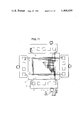
- FIG. 7 shows an exploded view of elements of the EL display panel assembly
- FIG. 8 shows a plan view of the EL display panel assembled to an inner chassis
- FIG. 9 shows an exploded view of the EL display assembly in which a printed circuit board is detached
- FIG. 10(a) shows a bottom view of the EL display panel assembly
- FIG. 10(b) shows a longitudinal sectional view of the assembly of FIG. 10(a);
- FIG. 11 shows a developing view of the combination of the flexible substrate and the EL display panel
- FIG. 12 shows a circuit diagram of the EL display panel assembly according to the present invention.
- FIG. 13 shows a circuit connection between the EL display panel and the flexible substrate
- FIG. 14 shows an exploded view of elements of the EL display panel assembly
- FIG. 15(a) shows a plan view of the EL display panel assembled to an inner chassis
- FIG. 15(b) shows a front view of the panel of FIG. 15(a);
- FIG. 15(c) shows a botton view of the panel of FIG. 15(a);
- FIG. 16(a) shows a plan view of the EL display panel assembly
- FIG. 16(b) shows a front view of the assembly of FIG. 16(a);
- FIG. 16(d) shows a partially cutaway view of the assembly of FIG. 16(a).
- FIG. 16(e) shows a longitudinal sectional view of the assembly of FIG. 16(a).
- the EL display panel assembly circuit comprises an EL display panel 10, integrated circuit (IC) drivers 20, 20', 21 and 21' and lines 30 for carrying signals and power energy.
- IC integrated circuit
- Each of the IC drivers 20 and 21' has output terminals from the first to the n-numbered one. It has additionally an input terminal IN and an output terminal OUT for inputting and outputting the data signals, respectively.
- a control terminal S is further provided in each.
- a specific output terminal OUT in one of the IC drivers is connected to a specific input terminal IN in another IC driver following said one.
- Each of the IC drivers has some shift registers.
- the direction of shifting data in any one of the shift registers is selective. More particularly, when the input signal applied to the control terminal S is in high level "H”, the data in the shift register are shifted from the first to the n-numbered output terminal. When the input signal applied to the control terminal S is in low level "L”, the data in the shift register are shifted from the n-numbered to the first output terminal.
- main surfaces of the IC drivers 20 and 21 are facing the front of a substrate for connecting to the EL display panel 10 while the opposite surfaces of the IC drivers 20' and 21' are facing the front of the substrate.
- FIG. 2 shows a developing view indicating a combination of the EL display panel assembly.
- This combination contains the IC drivers 20 1 to 20 4 and 20' 1 to 20' 4 flexible film substrates 70, 70', 71 and 71', and an EL display panel element 50.
- Each of the IC drivers contains some shift registers each for sending data in bi-directional directions.
- the IC drivers are arranged on the flexible film substrates.
- the flexible film substrates are attached to the EL display panel element 50.
- Markers are denoted as 80 and 80', indicating a particular location.
- Terminals are denoted as 90 and 90', supplying data signals and power energy.
- the output terminals OUT of the IC drivers 20 1 , 20 2 , 20 3 , 20' 1 , 20' 2 and 20' 3 are connected to the input terminals IN of the IC drivers 20 2 , 20 3 , 20 4 , 20' 2 , 20' 3 and 20' 4 .
- the input terminal IN of the IC driver 20 1 and the output terminal OUT of the In driver 20 4 are connected to the terminal 90.
- the input terminal N of the IC driver 20' 1 and the output terminal OUT of the IC driver 20' 4 are coupled to the terminal 90'.
- the control terminals S of the IC drivers 20 1 , 20 2 , 20 3 and 20 4 receive the input signal in the high level, the data signals are transferred from the input terminal IN of the IC driver 20 1 to the output terminal OUT of the IC driver 20 4 through the IC drivers 20 2 and 20 3 , these IC drivers being coupled in series.
- the EL display panel 50 is driven according to the so-called multiplex driving or the line-at-a-time operation.
- the data signals are transferred through the shift registers from the output terminal OUT of the IC driver 20' 4 to the input terminal IN of the IC driver 20' 1 through the IC drivers 20' 2 and 20' 3 , there IC drivers being coupled also in series.
- FIG. 3 shows a perspective view of the IC driver 20 connected to a substrate 40 similar to one of the flexible film substrates 70, 71, 70' and 71'.
- the IC driver 20 is lead-less ceramic chip carrier type.
- Output terminal electrodes of the IC driver 20 are denoted as 50 1 to 50 n .
- Soldering elements are denoted as 60 1 to 60n.
- Lead lines on the substrate 40 are denoted as 70 1 to 70 n .
- main surfaces of some IC drivers are confronting the front surface of substrate 40 on one side of the display panel while opposite surfaces of the remaining IC drivers are confronting the front of the substrate 40 on the opposite side of the display panel.
- FIG. 4 shows a developing view indicating the combination of the flexible film substrate and the EL display panel matrix according to the present invention.
- the drawing of FIG. 4 is similar to that of FIG. 2.
- the combination comprises a flexible film substrate B, IC drivers C, an EL display panel element A, and leads D.
- the IC drivers C are disposed on the substrate B.
- the IC drivers C comprise a driver, a shift register, a latch circuit, and a logic circuit etc.
- the number of the leads D necessary for controlling a plurality of X-axis electrodes and Y-axis electrodes on the EL display panel element A is minimized.
- the leads D contain 8 lines for data, clock (CR), latch, set, reset, ground (GND), power supply (VDD) for the EL display, and power supply (VSS) for the drivers.
- each of the X-axis electrodes and the Y-axis electrodes is lead out in one direction because of two of the flexible film substrates B, it is unnecessary to improve the number of the leads D. Further, when the number of the electrodes of the EL display panel is improved, it is unnecessary to improve the number of the leads D.
- a small number of leads D are lead out of the flexible film substrates B.
- FIGS. 5(a) through 5(c) show a specific example in which the flexible film substrate B is bent backward at the right angle and the IC drivers C on the substrate B are at right angle to the EL display panel A.
- FIGS. 6(a) through 6(c) show a specific example in which the flexible film substrate B is bent backward at the right angle and the IC drivers C on the substrate B are opposing to the EL display panel A.
- FIG. 7 shows an exploded view of the elements of the EL display panel assembly.
- the flexible film substrates B bent as shown in FIGS. 5(a) through 5(c) are used.
- An inner chasis E is provided, which has an insulating sheet in its sides. Corner elements I for alignment are provided on the front corners of the chassis E. The corner elements I support the corners of the EL display panel element A. The sides of the inner chassis E. touch with the flexible film substrate B as shown in FIG. 8.
- two pressing elements G may be provided.
- the pressing element G covers the upper flexible film substrate B and part of the side flexible film substrates B.
- An insulating sheet F may be interposed between the pressing element G and the substrate B.
- the inner chassis E it is possible that the EL display panel A and the flexible film substrates B are secured. Good resistance to mechanical shock can be obtained by the inner chassis E.
- the pressing element G provides protection for the flexible film substrates B and the IC drivers C etc. and assures thermal radiation.
- FIGS. 9, 10(a) and 10(b) show this embodiment.
- the inner chassis E supports the EL display panel A and the flexible film substrates B.
- the back of the chassis E is opened to reveal connectors K inside the chassis E.
- the printed circuit board J contains a control circuit and a power supply circuit etc.
- the board J is secured by the connectors K with a screw etc.
- the leads D on the substrates B are connected to circuit elements on the board J. This provides an improved compact circuit for the display system.
- FIGS. 11 through 14, 15(a) to 15(c) and 16(a) to 16(c) show a specific example of the EL display panel assembly.
- the EL display panel 1 involved has a size of 16 inches. It contains 160 terminals as the X-axis electrodes and 120 terminals as the Y-axis electrodes.
- polyamide film substrates 2 are used as specific flexible film substrates. Each of the substrates 2 supports IC drivers 3. The substrates 2 are coupled to the EL display panel 1. To the substrates 2, a display unit containing a flat cable 4, an inner chassis 6, pressing elements 9, a cover 10-1, and a printed circuit board 11 are connected.
- the inner chassis 6 has the corner members 7 to which the corners of the EL display panel 1 are secured.
- the polyamide film substrates 2 are bent along the sides of the inner chassis 6.
- An upper pressing element 9 1 is provided for covering the upper polyamide film substrate and part of the side polyamide film substrates.
- a lower pressing element 9 2 is provided for covering the lower polyamide film substrate and another part of the side polyamide film substrates.
- Insulating sheets 5 and 8 are interposed between the substrates 2 and the chassis 6.
- the cover 10-1 is secured to the combination of the EL display panel 1, the inner chassis 6, the polyamide film substrates 2 and the IC drivers 3.
- the printed circuit board 11 is disposed inside the inner chassis 6.
- the board 11 has a power supply circuit and a control circuit for controlling the IC drivers 3.
- the board 11 is fixed to terminals 13 of the chassis 6 with screws etc.
- the flat cable 4 is coupled to connectors 12 of the printed circuit board 11.
- FIG. 12 shows a circuit configuration of the EL display panel assembly.
- FIG. 12 indicates the EL display panel 1 and four of the IC drivers L around the panel 1.
- Each of the drivers L comprises shift registers (SR), latch circuits (LATCH), AND gates (AND), OR gates (OR), diodes (Di) and transistors (TR).
- the shift registers receive clock signals and data signals as input signals.
- the latch circuits receive output signals from the shift registers, and strobe signals as input signals.
- the AND gates receive, as input signals, the output signals from the latch circuits, and reset signals.
- the OR gates receive, as input signals, the output signals from the AND gates, and set signals.
- the diodes are provided for generating EL driving voltages in response to application of voltages.
- the transistors (TR) receive, as input signals, the output signals from the OR gates, and the EL driving voltages so as to drive the EL display panel.
- One of the IC drivers drives 32 electrodes in the EL display panel 1.
- the number of the IC drivers 3 for the X-axis electrodes is 5 in each side.
- the number of the IC drivers 3 for the Y-axis electrodes is 4 in each side.
- the flat cable 4 is connected to supply the clock signals (CR), the data signals (Data), the latch strobe signals (Strobe), the reset signals (Reset), the set signals (Set), power supply voltages (VDD) for anode common lines (A.C.) and power supply voltages (VSS) for logic circuits.
- the cover 10-1 has a window for entirely showing the front display surface of the EL display panel 1.
- the EL display panel 1 is fixed to the inner chassis 6.
- the EL display panel 1 together with the polyamide film substrates 2 is freely detachable from the back of the cover 10-1.
- the cover 10-1 can be fixed to the inner chassis 6 with screws etc.
Abstract
Description
Claims (15)
Applications Claiming Priority (6)
| Application Number | Priority Date | Filing Date | Title |
|---|---|---|---|
| JP11736580A JPS5741694A (en) | 1980-08-25 | 1980-08-25 | Electroluminescent display unit |
| JP55-117365 | 1980-08-25 | ||
| JP55119443A JPS5742073A (en) | 1980-08-28 | 1980-08-28 | Method of mounting panel display unit |
| JP55119444A JPS5742076A (en) | 1980-08-28 | 1980-08-28 | Electroluminiscent display unit |
| JP55-119443 | 1980-08-28 | ||
| JP55-119444 | 1980-08-28 |
Publications (1)
| Publication Number | Publication Date |
|---|---|
| US4468659A true US4468659A (en) | 1984-08-28 |
Family
ID=27313365
Family Applications (1)
| Application Number | Title | Priority Date | Filing Date |
|---|---|---|---|
| US06/294,245 Expired - Lifetime US4468659A (en) | 1980-08-25 | 1981-08-19 | Electroluminescent display panel assembly |
Country Status (3)
| Country | Link |
|---|---|
| US (1) | US4468659A (en) |
| DE (1) | DE3133618A1 (en) |
| GB (1) | GB2084778B (en) |
Cited By (31)
| Publication number | Priority date | Publication date | Assignee | Title |
|---|---|---|---|---|
| US4699470A (en) * | 1984-06-12 | 1987-10-13 | Taliq Corporation | NCAP liquid crystal apparatus incorporating a control means and an electrode means thereof incorporating a circuit means |
| US4730146A (en) * | 1986-10-21 | 1988-03-08 | W. H. Brady Co. | Folded electroluminescent lamp assembly |
| US4740781A (en) * | 1985-02-08 | 1988-04-26 | Itt Gilfillan | Touch panel data entry device for thin film electroluminescent panels |
| US4766426A (en) * | 1985-02-14 | 1988-08-23 | Matsushita Electric Industrial Co., Ltd. | Display panel assembly having a plurality of film carrier tapes on each of which a semiconductor divice is mounted |
| FR2611294A1 (en) * | 1987-02-23 | 1988-08-26 | Lohja Ab Oy | PLANAR DISPLAY DEVICE, PARTICULARLY ELECTROLUMINESCENT DISPLAY DEVICE |
| US4769753A (en) * | 1987-07-02 | 1988-09-06 | Minnesota Mining And Manufacturing Company | Compensated exponential voltage multiplier for electroluminescent displays |
| US4789858A (en) * | 1984-06-12 | 1988-12-06 | Taliq Corporation | Multifunction switch incorporating NCAP liquid crystal |
| US4806922A (en) * | 1987-09-23 | 1989-02-21 | Taliq Corporation | Display device utilizing a plurality of NCAP liquid crystal modules |
| US4808990A (en) * | 1983-11-11 | 1989-02-28 | Sharp Kabushiki Kaisha | Liquid crystal display assembly |
| US4859997A (en) * | 1986-12-16 | 1989-08-22 | Thomson-Csf | Display system for displaying essential data by separately handling different parts of the image to maximize reliability |
| US4982183A (en) * | 1988-03-10 | 1991-01-01 | Planar Systems, Inc. | Alternate polarity symmetric drive for scanning electrodes in a split-screen AC TFEL display device |
| US4984887A (en) * | 1988-03-23 | 1991-01-15 | Mitsubishi Denki Kabushiki Kaisha | Driving method for a flat panel display apparatus and the flat panel display apparatus |
| US5008656A (en) * | 1984-12-20 | 1991-04-16 | Raytheon Company | Flexible cable assembly |
| US5019807A (en) * | 1984-07-25 | 1991-05-28 | Staplevision, Inc. | Display screen |
| US5028916A (en) * | 1984-09-28 | 1991-07-02 | Kabushiki Kaisha Toshiba | Active matrix display device |
| WO1992014234A1 (en) * | 1991-01-31 | 1992-08-20 | Crystal Images, Inc. | Thermochromic image display apparatus |
| US5432015A (en) * | 1992-05-08 | 1995-07-11 | Westaim Technologies, Inc. | Electroluminescent laminate with thick film dielectric |
| US5563619A (en) * | 1993-03-22 | 1996-10-08 | Ncr Corporation | Liquid crystal display with integrated electronics |
| US5777610A (en) * | 1993-10-28 | 1998-07-07 | Sharp Kabushiki Kaisha | Small-sized, lightweight display device easy to rework and method of assembling the same |
| US20040004591A1 (en) * | 2002-05-17 | 2004-01-08 | Hajime Akimoto | Image display apparatus |
| US20070080917A1 (en) * | 2000-05-12 | 2007-04-12 | Semiconductor Engergy Laboratory Co., Ltd. | Display device |
| US20070176860A1 (en) * | 2006-02-02 | 2007-08-02 | Samsung Electronics Co., Ltd., | Display apparatus |
| US20070206127A1 (en) * | 2006-02-23 | 2007-09-06 | Chun-Seok Ko | Display device |
| US20080028601A1 (en) * | 2004-04-30 | 2008-02-07 | Lg Phillips Lcd Co., Ltd. | Structure for fixing printed circuit board and method of fixing thereof |
| US20080048948A1 (en) * | 2006-08-22 | 2008-02-28 | Samsung Electronics Co., Ltd. | Display device, flexible member, and method thereof |
| US20090073100A1 (en) * | 1999-04-16 | 2009-03-19 | Samsung Electronics Col, Ltd. | Signal transmission film and a liquid crystal display panel having the same |
| US20100224934A1 (en) * | 2004-12-06 | 2010-09-09 | Semiconductor Energy Laboratory Co., Ltd. | Display device |
| US8446348B2 (en) | 2003-06-13 | 2013-05-21 | Semiconductor Energy Laboratory Co., Ltd. | Display device |
| US8610645B2 (en) | 2000-05-12 | 2013-12-17 | Semiconductor Energy Laboratory Co., Ltd. | Display device |
| US20180122303A1 (en) * | 2016-11-02 | 2018-05-03 | Innolux Corporation | Display device |
| US20190146548A1 (en) * | 2017-11-10 | 2019-05-16 | Wuhan China Star Optoelectronics Semiconductor Display Technology Co., Ltd. | Display panel and display device |
Families Citing this family (7)
| Publication number | Priority date | Publication date | Assignee | Title |
|---|---|---|---|---|
| JPS6046581A (en) * | 1983-08-24 | 1985-03-13 | シャープ株式会社 | Package of device |
| CA1239468A (en) * | 1984-01-13 | 1988-07-19 | Yuji Watanabe | Video display system |
| GB8402654D0 (en) * | 1984-02-01 | 1984-03-07 | Secr Defence | Flatpanel display |
| US4613855A (en) * | 1984-03-05 | 1986-09-23 | Dale Electronics, Inc. | Direct current dot matrix plasma display having integrated drivers |
| GB2195196A (en) * | 1986-09-20 | 1988-03-30 | Emi Plc Thorn | Display device |
| JPH02296284A (en) * | 1989-05-11 | 1990-12-06 | Mitsubishi Electric Corp | Driver integration circuit device for display |
| CN107784940B (en) * | 2017-11-10 | 2019-11-05 | 武汉华星光电半导体显示技术有限公司 | Display panel and display device |
Citations (9)
| Publication number | Priority date | Publication date | Assignee | Title |
|---|---|---|---|---|
| US3668688A (en) * | 1969-12-29 | 1972-06-06 | Owens Illinois Inc | Gas discharge display and memory panel having addressing and interface circuits integral therewith |
| US3689131A (en) * | 1970-06-29 | 1972-09-05 | Rca Corp | Liquid crystal display device |
| US3705310A (en) * | 1970-05-27 | 1972-12-05 | Bbc Brown Boveri & Cie | Liquid crystal voltage display device having photoconductive means to enhance the contrast at the indicating region |
| US3928658A (en) * | 1972-04-28 | 1975-12-23 | Philips Corp | Method of providing transparent conductive electrodes on a transparent insulating support |
| US3974637A (en) * | 1975-03-28 | 1976-08-17 | Time Computer, Inc. | Light emitting diode wristwatch with angular display |
| US3975085A (en) * | 1973-10-31 | 1976-08-17 | Tokyo Shibaura Electric Co., Ltd. | Liquid crystal display device with interdigital electrodes |
| US4020627A (en) * | 1973-10-06 | 1977-05-03 | Citizen Watch Co., Ltd. | Liquid crystal display electronic watch |
| US4200868A (en) * | 1978-04-03 | 1980-04-29 | International Business Machines Corporation | Buffered high frequency plasma display system |
| US4231640A (en) * | 1977-07-07 | 1980-11-04 | Sharp Kabushiki Kaisha | Matrix type liquid crystal display panel |
Family Cites Families (5)
| Publication number | Priority date | Publication date | Assignee | Title |
|---|---|---|---|---|
| DE2441699A1 (en) * | 1974-08-30 | 1976-03-11 | Daut & Rietz Kg | Holder for display carriers, partic liquid crystal displays - comprises rotary closed frame with connecting springs in batten |
| DE2620165A1 (en) * | 1976-05-07 | 1977-11-17 | Joachim Sylla | Safety darkness visibility aid for pedestrians - comprises array of light elements connected via electronic timing and sampling circuit and amplifier elements to current source |
| FR2388460A1 (en) * | 1977-04-20 | 1978-11-17 | Yema | Printed circuit with provision for discrete component connection - has flexible substrate with folded connection strips bent into tight U=shape |
| DE2748899A1 (en) * | 1977-11-02 | 1979-05-10 | John Anderson | Electroluminescent display screen - has matrix of display points activated by digitised form of analogue signal |
| US4287449A (en) * | 1978-02-03 | 1981-09-01 | Sharp Kabushiki Kaisha | Light-absorption film for rear electrodes of electroluminescent display panel |
-
1981
- 1981-08-19 US US06/294,245 patent/US4468659A/en not_active Expired - Lifetime
- 1981-08-24 GB GB8125804A patent/GB2084778B/en not_active Expired
- 1981-08-25 DE DE19813133618 patent/DE3133618A1/en active Granted
Patent Citations (9)
| Publication number | Priority date | Publication date | Assignee | Title |
|---|---|---|---|---|
| US3668688A (en) * | 1969-12-29 | 1972-06-06 | Owens Illinois Inc | Gas discharge display and memory panel having addressing and interface circuits integral therewith |
| US3705310A (en) * | 1970-05-27 | 1972-12-05 | Bbc Brown Boveri & Cie | Liquid crystal voltage display device having photoconductive means to enhance the contrast at the indicating region |
| US3689131A (en) * | 1970-06-29 | 1972-09-05 | Rca Corp | Liquid crystal display device |
| US3928658A (en) * | 1972-04-28 | 1975-12-23 | Philips Corp | Method of providing transparent conductive electrodes on a transparent insulating support |
| US4020627A (en) * | 1973-10-06 | 1977-05-03 | Citizen Watch Co., Ltd. | Liquid crystal display electronic watch |
| US3975085A (en) * | 1973-10-31 | 1976-08-17 | Tokyo Shibaura Electric Co., Ltd. | Liquid crystal display device with interdigital electrodes |
| US3974637A (en) * | 1975-03-28 | 1976-08-17 | Time Computer, Inc. | Light emitting diode wristwatch with angular display |
| US4231640A (en) * | 1977-07-07 | 1980-11-04 | Sharp Kabushiki Kaisha | Matrix type liquid crystal display panel |
| US4200868A (en) * | 1978-04-03 | 1980-04-29 | International Business Machines Corporation | Buffered high frequency plasma display system |
Cited By (58)
| Publication number | Priority date | Publication date | Assignee | Title |
|---|---|---|---|---|
| US4808990A (en) * | 1983-11-11 | 1989-02-28 | Sharp Kabushiki Kaisha | Liquid crystal display assembly |
| US4789858A (en) * | 1984-06-12 | 1988-12-06 | Taliq Corporation | Multifunction switch incorporating NCAP liquid crystal |
| USRE33921E (en) * | 1984-06-12 | 1992-05-12 | Taliq Corporation | NCAP liquid crystal apparatus incorporating a control means and electrode means thereof incorporating a circuit means |
| US4699470A (en) * | 1984-06-12 | 1987-10-13 | Taliq Corporation | NCAP liquid crystal apparatus incorporating a control means and an electrode means thereof incorporating a circuit means |
| US5019807A (en) * | 1984-07-25 | 1991-05-28 | Staplevision, Inc. | Display screen |
| US5028916A (en) * | 1984-09-28 | 1991-07-02 | Kabushiki Kaisha Toshiba | Active matrix display device |
| US5008656A (en) * | 1984-12-20 | 1991-04-16 | Raytheon Company | Flexible cable assembly |
| US4740781A (en) * | 1985-02-08 | 1988-04-26 | Itt Gilfillan | Touch panel data entry device for thin film electroluminescent panels |
| US4766426A (en) * | 1985-02-14 | 1988-08-23 | Matsushita Electric Industrial Co., Ltd. | Display panel assembly having a plurality of film carrier tapes on each of which a semiconductor divice is mounted |
| US4730146A (en) * | 1986-10-21 | 1988-03-08 | W. H. Brady Co. | Folded electroluminescent lamp assembly |
| US4859997A (en) * | 1986-12-16 | 1989-08-22 | Thomson-Csf | Display system for displaying essential data by separately handling different parts of the image to maximize reliability |
| FR2611294A1 (en) * | 1987-02-23 | 1988-08-26 | Lohja Ab Oy | PLANAR DISPLAY DEVICE, PARTICULARLY ELECTROLUMINESCENT DISPLAY DEVICE |
| US4769753A (en) * | 1987-07-02 | 1988-09-06 | Minnesota Mining And Manufacturing Company | Compensated exponential voltage multiplier for electroluminescent displays |
| US4806922A (en) * | 1987-09-23 | 1989-02-21 | Taliq Corporation | Display device utilizing a plurality of NCAP liquid crystal modules |
| US4982183A (en) * | 1988-03-10 | 1991-01-01 | Planar Systems, Inc. | Alternate polarity symmetric drive for scanning electrodes in a split-screen AC TFEL display device |
| US4984887A (en) * | 1988-03-23 | 1991-01-15 | Mitsubishi Denki Kabushiki Kaisha | Driving method for a flat panel display apparatus and the flat panel display apparatus |
| WO1992014234A1 (en) * | 1991-01-31 | 1992-08-20 | Crystal Images, Inc. | Thermochromic image display apparatus |
| US5202677A (en) * | 1991-01-31 | 1993-04-13 | Crystal Images, Inc. | Display apparatus using thermochromic material |
| US5702565A (en) * | 1992-05-08 | 1997-12-30 | Westaim Technologies, Inc. | Process for laser scribing a pattern in a planar laminate |
| US5756147A (en) * | 1992-05-08 | 1998-05-26 | Westaim Technologies, Inc. | Method of forming a dielectric layer in an electroluminescent laminate |
| US5634835A (en) * | 1992-05-08 | 1997-06-03 | Westaim Technologies Inc. | Electroluminescent display panel |
| US5679472A (en) * | 1992-05-08 | 1997-10-21 | Westaim Technologies, Inc. | Electroluminescent laminate and a process for forming address lines therein |
| US5432015A (en) * | 1992-05-08 | 1995-07-11 | Westaim Technologies, Inc. | Electroluminescent laminate with thick film dielectric |
| US5563619A (en) * | 1993-03-22 | 1996-10-08 | Ncr Corporation | Liquid crystal display with integrated electronics |
| US5777610A (en) * | 1993-10-28 | 1998-07-07 | Sharp Kabushiki Kaisha | Small-sized, lightweight display device easy to rework and method of assembling the same |
| CN1120458C (en) * | 1993-10-28 | 2003-09-03 | 夏普公司 | Display device easy to rework and method of assembling the same |
| US20090073100A1 (en) * | 1999-04-16 | 2009-03-19 | Samsung Electronics Col, Ltd. | Signal transmission film and a liquid crystal display panel having the same |
| US8610645B2 (en) | 2000-05-12 | 2013-12-17 | Semiconductor Energy Laboratory Co., Ltd. | Display device |
| US10867557B2 (en) | 2000-05-12 | 2020-12-15 | Semiconductor Energy Laboratory Co., Ltd. | Display device |
| US10354589B2 (en) | 2000-05-12 | 2019-07-16 | Semiconductor Energy Laboratory Co., Ltd. | Display device |
| US20070080917A1 (en) * | 2000-05-12 | 2007-04-12 | Semiconductor Engergy Laboratory Co., Ltd. | Display device |
| US8125415B2 (en) | 2000-05-12 | 2012-02-28 | Semiconductor Energy Laboratory Co., Ltd. | Display device |
| US9536468B2 (en) | 2000-05-12 | 2017-01-03 | Semiconductor Energy Laboratory Co., Ltd. | Display device |
| US9013377B2 (en) | 2000-05-12 | 2015-04-21 | Semiconductor Energy Laboratory Co., Ltd. | Display device |
| US9514670B2 (en) | 2000-05-12 | 2016-12-06 | Semiconductor Energy Laboratory Co., Ltd. | Display device |
| US20040004591A1 (en) * | 2002-05-17 | 2004-01-08 | Hajime Akimoto | Image display apparatus |
| US7733309B2 (en) * | 2002-05-17 | 2010-06-08 | Hitachi, Ltd. | Image display apparatus |
| US9905582B2 (en) | 2003-06-13 | 2018-02-27 | Semiconductor Energy Laboratory Co., Ltd. | Display device |
| US9276018B2 (en) | 2003-06-13 | 2016-03-01 | Semiconductor Energy Laboratory Co., Ltd. | Display device |
| US9030389B2 (en) | 2003-06-13 | 2015-05-12 | Semiconductor Energy Laboratory Co., Ltd. | Display device |
| US8446348B2 (en) | 2003-06-13 | 2013-05-21 | Semiconductor Energy Laboratory Co., Ltd. | Display device |
| US8749461B2 (en) | 2003-06-13 | 2014-06-10 | Semiconductor Energy Laboratory Co., Ltd. | Display device |
| US7631421B2 (en) * | 2004-04-30 | 2009-12-15 | Lg Display Co., Ltd. | Method for fixing printed circuit board on a display panel |
| US20080028601A1 (en) * | 2004-04-30 | 2008-02-07 | Lg Phillips Lcd Co., Ltd. | Structure for fixing printed circuit board and method of fixing thereof |
| US8547315B2 (en) | 2004-12-06 | 2013-10-01 | Semiconductor Energy Laboratory Co., Ltd. | Display device |
| US8717269B2 (en) | 2004-12-06 | 2014-05-06 | Semiconductor Energy Laboratory Co., Ltd. | Display device |
| US8228277B2 (en) | 2004-12-06 | 2012-07-24 | Semiconductor Energy Laboratory Co., Ltd. | Display device |
| US9123625B2 (en) | 2004-12-06 | 2015-09-01 | Semiconductor Energy Laboratory Co., Ltd. | Display device |
| US8102347B2 (en) | 2004-12-06 | 2012-01-24 | Semiconductor Energy Laboratory Co., Ltd. | Display device |
| US20100224934A1 (en) * | 2004-12-06 | 2010-09-09 | Semiconductor Energy Laboratory Co., Ltd. | Display device |
| US20070176860A1 (en) * | 2006-02-02 | 2007-08-02 | Samsung Electronics Co., Ltd., | Display apparatus |
| US20070206127A1 (en) * | 2006-02-23 | 2007-09-06 | Chun-Seok Ko | Display device |
| US7633746B2 (en) | 2006-02-23 | 2009-12-15 | Samsung Electronics Co., Ltd. | Display device |
| US20080048948A1 (en) * | 2006-08-22 | 2008-02-28 | Samsung Electronics Co., Ltd. | Display device, flexible member, and method thereof |
| US20180122303A1 (en) * | 2016-11-02 | 2018-05-03 | Innolux Corporation | Display device |
| US10546537B2 (en) * | 2016-11-02 | 2020-01-28 | Innolux Corporation | Display device with display drivers arranged on edge thereof |
| US20190146548A1 (en) * | 2017-11-10 | 2019-05-16 | Wuhan China Star Optoelectronics Semiconductor Display Technology Co., Ltd. | Display panel and display device |
| US10509436B2 (en) * | 2017-11-10 | 2019-12-17 | Wuhan China Star Optoelectronics Semiconductor Display Technology Co., Ltd. | Display panel and display device |
Also Published As
| Publication number | Publication date |
|---|---|
| DE3133618C2 (en) | 1987-03-12 |
| GB2084778B (en) | 1984-12-05 |
| GB2084778A (en) | 1982-04-15 |
| DE3133618A1 (en) | 1982-08-12 |
Similar Documents
| Publication | Publication Date | Title |
|---|---|---|
| US4468659A (en) | Electroluminescent display panel assembly | |
| US6160605A (en) | Display device with particular external connections | |
| US20050205877A1 (en) | Display device having driving circuit | |
| US5462442A (en) | Module for information processing apparatus using stacked printed circuit boards and connector for stacking printed circuit boards | |
| US7012667B2 (en) | Liquid crystal display device | |
| GB1585394A (en) | Display arrangements | |
| GB2145561A (en) | Driver device mounting | |
| CN113539168B (en) | Driver circuit and display device | |
| JPS6315591B2 (en) | ||
| KR100665184B1 (en) | Semiconductor chip, Tape Carrier PackageTCP mounted on the chip and Liquid Crystal Display device including the TCP | |
| CN100507642C (en) | Liquid crystal display device | |
| US6356252B2 (en) | Apparatus for supplying gray level compensating voltage | |
| US5260698A (en) | Integrated circuit for liquid crystal display | |
| CN114938677A (en) | Light-emitting substrate and display device | |
| JPH0648541Y2 (en) | Liquid crystal display | |
| JPH032935Y2 (en) | ||
| JPH11126792A (en) | Electrode position of face-down type multi-output driver, electrode position of face-down type ic, wiring board and display module | |
| WO2024024516A1 (en) | Communication device, drive device, display device, and communication method | |
| CN115188278B (en) | Display module and display device | |
| EP0261369B1 (en) | Integrated circuit for liquid crystal display | |
| JP2846802B2 (en) | EL display device | |
| JPH086058A (en) | Liquid crystal display device | |
| US6577318B1 (en) | Integrated circuit device and display device with the same | |
| JPH07302066A (en) | Liquid crystal display device | |
| JP4581327B2 (en) | Wiring board, display module, and electronic device |
Legal Events
| Date | Code | Title | Description |
|---|---|---|---|
| AS | Assignment |
Owner name: SHARP KABUSHIKI KAISHA, 22-22 NAGAIKE-CHO,ABENO-KU Free format text: ASSIGNMENT OF ASSIGNORS INTEREST.;ASSIGNORS:OHBA, TOSHIHIRO;KANATANI, YOSHIHARU;KINOSHITA, HIROSHI;AND OTHERS;REEL/FRAME:003911/0076 Effective date: 19810810 |
|
| STCF | Information on status: patent grant |
Free format text: PATENTED CASE |
|
| FPAY | Fee payment |
Year of fee payment: 4 |
|
| FEPP | Fee payment procedure |
Free format text: PAYOR NUMBER ASSIGNED (ORIGINAL EVENT CODE: ASPN); ENTITY STATUS OF PATENT OWNER: LARGE ENTITY |
|
| FPAY | Fee payment |
Year of fee payment: 8 |
|
| FEPP | Fee payment procedure |
Free format text: PAYER NUMBER DE-ASSIGNED (ORIGINAL EVENT CODE: RMPN); ENTITY STATUS OF PATENT OWNER: LARGE ENTITY Free format text: PAYOR NUMBER ASSIGNED (ORIGINAL EVENT CODE: ASPN); ENTITY STATUS OF PATENT OWNER: LARGE ENTITY |
|
| FPAY | Fee payment |
Year of fee payment: 12 |