US4472738A - Pattern testing apparatus - Google Patents
Pattern testing apparatus Download PDFInfo
- Publication number
- US4472738A US4472738A US06/381,469 US38146982A US4472738A US 4472738 A US4472738 A US 4472738A US 38146982 A US38146982 A US 38146982A US 4472738 A US4472738 A US 4472738A
- Authority
- US
- United States
- Prior art keywords
- area
- pattern
- digital signals
- detection
- defect
- Prior art date
- Legal status (The legal status is an assumption and is not a legal conclusion. Google has not performed a legal analysis and makes no representation as to the accuracy of the status listed.)
- Expired - Fee Related
Links
Images


Classifications
-
- G—PHYSICS
- G01—MEASURING; TESTING
- G01N—INVESTIGATING OR ANALYSING MATERIALS BY DETERMINING THEIR CHEMICAL OR PHYSICAL PROPERTIES
- G01N21/00—Investigating or analysing materials by the use of optical means, i.e. using sub-millimetre waves, infrared, visible or ultraviolet light
- G01N21/84—Systems specially adapted for particular applications
- G01N21/88—Investigating the presence of flaws or contamination
- G01N21/95—Investigating the presence of flaws or contamination characterised by the material or shape of the object to be examined
- G01N21/956—Inspecting patterns on the surface of objects
-
- G—PHYSICS
- G06—COMPUTING; CALCULATING OR COUNTING
- G06T—IMAGE DATA PROCESSING OR GENERATION, IN GENERAL
- G06T7/00—Image analysis
- G06T7/0002—Inspection of images, e.g. flaw detection
- G06T7/0004—Industrial image inspection
- G06T7/001—Industrial image inspection using an image reference approach
-
- G—PHYSICS
- G06—COMPUTING; CALCULATING OR COUNTING
- G06T—IMAGE DATA PROCESSING OR GENERATION, IN GENERAL
- G06T2207/00—Indexing scheme for image analysis or image enhancement
- G06T2207/10—Image acquisition modality
- G06T2207/10016—Video; Image sequence
-
- G—PHYSICS
- G06—COMPUTING; CALCULATING OR COUNTING
- G06T—IMAGE DATA PROCESSING OR GENERATION, IN GENERAL
- G06T2207/00—Indexing scheme for image analysis or image enhancement
- G06T2207/30—Subject of image; Context of image processing
- G06T2207/30108—Industrial image inspection
- G06T2207/30148—Semiconductor; IC; Wafer
Definitions
- the present invention relates to a pattern testing apparatus which tests a digitized video signal derived from an image of a two-dimensional pattern such as a mask or a reticle used in the IC manufacture, with respect to a design pattern to detect a defect.
- a digitized video signal derived by imaging a pattern under test is compared with a design value.
- the method (3) above is relevant to the present invention. It utilizes a feature that a pattern width and a pattern-to-pattern interval of a pattern printed on the mask or reticle are always wider than a design width or a width of a pattern rule and an angle between patterns is constant. If the pattern under test has a narrower pattern than the width of the pattern rule or an angle which is not found in the pattern rule, a defect is detected. Since this method relies only on the characteristics of the pattern, no registration is required and a discrete defect which is smaller than the width of the pattern rule and a defect having a smaller pattern than the width of the pattern rule can be detected with a high precision by a simple logic circuit. However, even in the method (3) above, a special portion of a normal pattern such as an end of a right angle edge having a slope of 45 degrees may be misjudged as a defect.
- a first area and a second area are defined on the two-dimensional pattern, and means is provided for receiving digital signals one for each of the picture cells of the first and second areas and discriminating the presence of a defect in the second area when it detects that all of the picture cells of the first area have the same logical value and at least one of the picture cells of the second area has a logical value different from the logical value of the picture cells of the first area.
- the second area is generally rectangular shape having two opposing sides of a first length which is shorter than a width of a pattern rule and two opposing sides having a second length which is longer than the first length with at least one of the two opposing sides of the first length being concaved by at no smaller than one-half of the first length, and the first area has two equal sub-areas adjacent to the two opposing sides of the second length of the second area to sandwitch the second area are defined on the two-dimensional pattern.
- the concave area is defined by an arc of a circle having a diameter equal to the first length and a chord having a length equal to the first length.
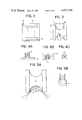
- FIG. 1 shows a block diagram of a configuration of a pattern testing apparatus of the present invention
- FIG. 2 shows a chart for explaining a portion of operation of the present invention
- FIG. 3 shows a detection area defined by a template in accordance with the present invention
- FIGS. 4A to 4C and 5A to 5B show charts for explaining other portions of the operation of the present invention
- FIGS. 6A to 6C, 10 and 11 show various detection areas used in the present invention
- FIGS. 7A to 7D show windows and templates corresponding to the detection area shown in FIG. 3,
- FIG. 8 shows one embodiment of a circuit for the template shown in FIG. 7A
- FIG. 9 shows a template corresponding to the detection area shown in FIG. 6C
- FIG. 10 shows an embodiment of a circuit for the template shown in FIG. 9,
- FIG. 12 shows a window and a template corresponding to the detection area shown in FIG. 11, and
- FIG. 13 shows an embodiment of a circuit for the template shown in FIG. 11.
- FIG. 1 shows a block diagram of a configuration of the present invention.
- a two-dimensional pattern such as a mask or a reticle in the IC manufacture is converted to an analog video signal representing a density of the pattern by an imaging device 1, and the analog video signal is converted by a digitizer 2 to a two-valued digital signal in synchronism with a clock pulse generated by a clock pulse generator, not shown.
- a filter circuit or smoothing circuit 3 eliminates a noise component included in the digital signal and supplies the digital signal to a set of shift registers 4 in synchronism with the clock pulse.
- the shift registers 4 sequentially store and shift the digital signal in the form of two logical values represented by two signals in synchronism with the clock pulse.
- the shift registers 4 comprise n registers 411, 412, . . . 41n and n-1 registers 421, 422, . . . 42n-1.
- the sums of the registers 411 and 421, 412, and 422, . . . ,41n-1 and 42n-1, respectively, are equal to the number of picture cells in one horizontal scan line of the imaging device 1.
- the shift registers 411, 412, . . . 41n have m bit positions A 11 , A 12 . . . A 1m ; A 21 , A 22 , . . . A 2n ; . . .; A n1 , A n2 , . . . A nm , respectively.
- Hatched areas shown in FIG. 2 are windows 8 each of which comprises nxm picture cells loaded to the shift registers 411, 412, . . . 41n from the reticle or pattern 9.
- a first detection circuits 5 and a second detection circuit 6 sequentially receive the digital signal corresponding to the picture cells to be detected which are in the window 8, from the shift registers 411, 412, . . . 41n in synchronism with the clock pulse.
- the picture cells to be detected by the first detection circuit 5 and the second detection circuit 6, respectively, are called templates.
- detection areas 11 and 12 are defined by the template associated with the first detection circuit 5, and a detection area 13 is defined by the template associated with the second detection circuit 6.
- the first detection circuit 5 and the second detection circuit 6 receive the digital signals representing the density of the picture cells in the corresponding templates and supply detection signals to a discrimination circuit 7, which checks any defect in the area based on the detection signal.
- the detection areas 11 and 12 correspond to the template associated with the first detection circuit 5 and the detection area 13 corresponds to the template associated with the second detection circuit 6.
- a template inner width ⁇ i, a template length l and a template radius r have the following relations.
- W 0 is a pattern rule width
- ⁇ is a thinning/thickening factor of the pattern in pre-processing by the digitizer 2 and the filter circuit 3 (the template inner width ⁇ i is always narrower than the pattern rule width W 0 in the window 8), and ⁇ is a width permitted for roundness of a corner of the pattern per se, roundness of the corner of the pattern due to the pre-processing, and irregularity of pattern boundary.
- a concaved area defined by an arc having a radius r is formed in the detection area 13 to prevent misdetection of a normal pattern as a defect, as will be explained later with reference to FIGS. 5A and 5B.
- the shapes and the sizes of the detection areas 11, 12 and 13 are defined in this manner, and logical values for the picture cells forming the detection areas 11, 12 and 13 are defined as follows:
- the mask or reticle pattern comprises dark areas and light areas and the dark areas are represented by logical value "1" and the light areas are represented by logical value "0".
- Both the expressions (1a) and (1b) simultaneously assume "1" when all of the logical values ai and bj representing the picture cells forming the detection areas 11 and 12 are of the same logical value and at least one of the logical values ci representing the picture cells forming the detection area 13 is different from the logical value of ai and bi.
- a smaller pattern than the pattern rule width W 0 exists and it should be regarded as a defect.
- a hatched area represents the dark area and a non-hatched area represents the light area.
- DEFB in the expression (1a) assumes "1" and the dark area defect is detected.
- DEFW in the expression (1b) assumes "1" and the light area defect is detected.
- the second term of the right side of each of the expressions (1a) and (1b) is "0" when the first term thereof is “1", and the first term is "0" when the second term is "1". Accordingly, the normal design pattern is not misdetected as a defect.
- a round corner of the pattern can also be correctly detected.
- the detection area shown in FIG. 3 can mainly detect the defect having a vertical component as shown in FIGS. 4A and 4B.
- a detection area for detecting a defect having a horizontal component as shown in FIG. 6A a detection area for detecting a defect in a 45-degree direction as shown in FIG. 6B and a detection area for detecting a defect in a 135-degree direction as shown in FIG. 6C
- the defects having horizontal, 45-degree and 135-degree components and the discrete defect can be detected.
- the detection areas having 15-degree, 30-degree, 60-degree, 75-degree, 105-degree, 120-degree, 150-degree and 165-degree directivities may be provided.
- a detection sensitivity is fixed depending on the size of the defect for the defect near the boundary of the dark area and the light area. Accordingly, by providing the detection areas of various sizes and various directivities within a range which meets a condition that the template inner width ⁇ i is narrower than W 0- ⁇ , all of the small defects can be detected and the types of the defects such as sizes and directions can be determined.
- the window 8 of the template is now explained. It is now assumed that the pattern rule width W 0 is eight picture cell length, the thinning or thickening of the pattern by the pre-processing is one picture cell length, and the roundness of the corner of the pattern and the irregurality ⁇ of the pattern boundary are one picture cell length, respectively. Under such an assumption, the width of the mask or reticle pattern, when it is digitized, may assume 7 to 9 picture cell length. Accordingly for the vertical and horizontal directivity templates, the template inner width ⁇ i may be 2, 4, 5 and 6 picture cell length. FIGS. 7A to 7D show the templates for the vertical directivity detection area.
- the window 8 is divided into 11 ⁇ 11 picture cells and the templates for defining the detection areas for detecting the vertical directivity defects are shown for the template inner width ⁇ i of 3 to 6 picture cell length.
- the 11 ⁇ 11 picture cells are defined by rows A, B, . . . K and columns 1, 2, . . . 11.
- a left line of picture cells designated by "1” correspond to the detection area 11
- a right line of picture cells designated by "1" correspond to the detection area 12
- the picture cells designated by "0" correspond to the detection area 13.
- the picture cells designated by “1” represent the template associated with the first detection circuit 5 and the picture cells designated by "0" represent the template associated with the second detection circuit 6.
- the first detection circuit 5, the second detection circuit 6 and the discrimination circuit 7 carry out the logical operations in accordance with the expressions (1a) and (1b) described above.
- the first detection circuit 5, the second detection circuit 6 and the discrimination circuit 7 are constructed as shown in FIG. 8.
- the logical values of the picture cells D4, E4, F4, G4 and H4 corresponding to the detection area 11 are designated by a 1 , a 2 , . . . a 5 , respectively, the logical values of the picture cells D8, E8, F8, G8 and H8 corresponding to the detection area 12 are designated by b 1 , b 2 , . .
- the first detection circuit 5 is an AND gate which receives the digital signals having the logical values a 1 ⁇ a 5 and b 1 ⁇ b 5
- the second detection circuit 6 is an OR gate which receives the digital signals having the logical values of inversions of c 1 ⁇ c 3
- the discrimination circuit 7 is an AND gate.
- the second detection circuit 6 may be a NAND gate which receives the digital signals having the logical values c 1 ⁇ c 3 .
- the first detection circuit 5 is an AND gate which receives the digital signals having the logical values of inversions of a 1 ⁇ a 5 and b 1 ⁇ b 5
- the second detection circuit 6 is an OR gate which receives the digital signals having the logical values c 1 ⁇ c 3
- the discrimination circuit 7 is an AND gate, as is apparent from the expression (1a).
- the first detection circuit 5 may be a NOR gate which receives the digital signals having the logical values a 1 ⁇ a 5 and b 1 ⁇ b 5 .
- the first detection circuits 5, the second detection circuits 6 and the discrimination circuits 7 for the templates shown in FIGS. 7B to 7D can be similarly constructed.
- the discrimination circuit 7 detects a defect in one of the picture cells, for example, the picture cell F6, in the template associated with the second detection circuit 6.
- FIG. 9 shows a 135-degree directivity template corresponding to the detection area shown in FIG. 6C.
- the template associated with the first detection circuit 5, which is shown by the picture cells designated by "1" is defined not only by the picture cells F2, G3, H4, I5 and J6 and the picture cells B6, C7, D8, E9 and F10 having the logical values a 1 ⁇ a 5 and b 1 ⁇ b 5 , respectively, but also by additional picture elements H3 and I4 and picture elements C8 and D9 having logical values of a 6 , a 7 and b 6 , b 7 , respectively.
- the template associated with the second detection circuit 6, which is shown by the picture cells designated by "1" is defined by the picture cells E7, F6, G5, G4, H5, D7 and E8 having logical values c 1 ⁇ c 7 , respectively.
- the first detection circuit 5, the second detection circuit 6 and the discrimination circuit 7 may be constructed as shown in FIG. 8.
- FIG. 10 shows an embodiment of the construction of the first detection circuit 5, the second detection circuit 6 and the discrimination circuit 7 for detecting the light area defect in the template shown in FIG. 9. A similar effect can be attained even if the picture cells G4, H5 and D7, E8 are not used in the defect detection logic.
- FIG. 11 shows a detection area defined by a template for detecting a small discrete defect.
- a hatched area 13' is a circle having a diameter ⁇ i and a ring area 14' intersects the area 13' from an external area.
- the logical values of the picture cells forming the area 14' and the area 13' are defined as follows, respectively:
- FIG. 12 shows an example of the template in the window 8 corresponding to the detection area shown in FIG. 11.
- the template associated with the first detection circuit 5, which is shown by the picture cells designated by "1" is defined by the picture cells D6, D7, E5, E8, F4, F10, G4, G10, H5, H8, I6, and I7 having logical values ab 1 , ab 2 , . . . ab 12 , respectively.
- the template associated with the second detection circuit 6, which is shown by the picture cells designated by "0” is defined by the picture cells F6, F7, G6 and G7 having the logical values c 1 ', c 2 '. . . C 4 ', respectively.
- the expressions (1a') and (1b') correspond to the expressions (1a) and (1b), respectively.
- the first detection circuit 5, the second detection circuit 6 and the discrimination circuit 7 may be constructed as shown in FIG. 8.
- FIG. 13 shows an embodiment of the construction of the first detection circuit 5, the second detection circuit 6 and the discrimination circuit 7 for detecting the discrete light area defect in the template shown in FIG. 12.
Abstract
Description
φi<W.sub.0 -ω
r=φi/2
l>2r+2δ
ai(i=1˜k)
bj(j=1˜k)
ck(k=1˜l)
DEFB=(a.sub.1 ·b.sub.1 ·a.sub.2 ·b.sub.2. . . a.sub.k ·b.sub.k)·(c.sub.1 +c.sub.2 +. . . c.sub.l) (1a)
DEFW=(a.sub.1 ·b.sub.1 ·a.sub.2 ·b.sub.2 ·. . . a.sub.k ·b.sub.k)·(c.sub.1 +c.sub.2 +. . . c.sub.l) (1b)
abi(i=1˜k')
c'k(k=1˜l')
DEFB'=(ab.sub.1 ·ab.sub.2 . . . ab.sub.k')·(c'.sub.1 +c'.sub.2 +. . . c'.sub.l') (1a')
DEFW'=(ab.sub.1 ·ab.sub.2 ·. . . ab.sub.k')·(c'.sub.1 +c'.sub.2 +. . . c'.sub.l') (1b')
Claims (2)
Applications Claiming Priority (2)
| Application Number | Priority Date | Filing Date | Title |
|---|---|---|---|
| JP56083373A JPS57198851A (en) | 1981-05-30 | 1981-05-30 | Inspecting device for defect of pattern |
| JP56-83373 | 1981-05-30 |
Publications (1)
| Publication Number | Publication Date |
|---|---|
| US4472738A true US4472738A (en) | 1984-09-18 |
Family
ID=13800611
Family Applications (1)
| Application Number | Title | Priority Date | Filing Date |
|---|---|---|---|
| US06/381,469 Expired - Fee Related US4472738A (en) | 1981-05-30 | 1982-05-24 | Pattern testing apparatus |
Country Status (2)
| Country | Link |
|---|---|
| US (1) | US4472738A (en) |
| JP (1) | JPS57198851A (en) |
Cited By (7)
| Publication number | Priority date | Publication date | Assignee | Title |
|---|---|---|---|---|
| US4532650A (en) * | 1983-05-12 | 1985-07-30 | Kla Instruments Corporation | Photomask inspection apparatus and method using corner comparator defect detection algorithm |
| WO1986001920A1 (en) * | 1984-09-21 | 1986-03-27 | Hughes Aircraft Co | Target discrimination utilizing median filters |
| US4633504A (en) * | 1984-06-28 | 1986-12-30 | Kla Instruments Corporation | Automatic photomask inspection system having image enhancement means |
| US4641353A (en) * | 1983-09-16 | 1987-02-03 | Fujitsu Limited | Inspection method and apparatus for a mask pattern used in semiconductor device fabrication |
| EP0290228A2 (en) * | 1987-05-08 | 1988-11-09 | Qc Optics, Inc. | Surface defect detection and confirmation system and method |
| US6775899B1 (en) * | 1999-05-24 | 2004-08-17 | Matsushita Electric Industrial Co., Ltd. | Method for inspecting printing state and substrate |
| US20070005279A1 (en) * | 2005-06-28 | 2007-01-04 | Boerstler David W | System and method for examining high-frequency clock-masking signal patterns at full speed |
Families Citing this family (3)
| Publication number | Priority date | Publication date | Assignee | Title |
|---|---|---|---|---|
| JPS59121563A (en) * | 1982-12-28 | 1984-07-13 | Fujitsu Ltd | Device for correcting design data of integrated circuit |
| JPS59159531A (en) * | 1983-03-01 | 1984-09-10 | Nec Corp | Pinhole detector |
| CN108961221B (en) * | 2018-06-15 | 2021-09-07 | 哈尔滨工业大学 | Aviation plug field static image detection algorithm |
Citations (5)
| Publication number | Priority date | Publication date | Assignee | Title |
|---|---|---|---|---|
| US4124865A (en) * | 1976-12-06 | 1978-11-07 | Hughes Aircraft Company | Automatic reticle detection and tracking method and system |
| US4319269A (en) * | 1978-11-24 | 1982-03-09 | Kanebo Limited | External appearance inspecting system |
| US4353087A (en) * | 1979-03-12 | 1982-10-05 | The Perkin-Elmer Corporation | Automatic mask alignment |
| US4364089A (en) * | 1979-10-31 | 1982-12-14 | Westinghouse Electric Corp. | Binary correlation video tracker |
| US4380025A (en) * | 1979-08-06 | 1983-04-12 | Ball Corporation | Auxiliary blanking and auxiliary simulated video line generator unit for a video inspection system |
Family Cites Families (3)
| Publication number | Priority date | Publication date | Assignee | Title |
|---|---|---|---|---|
| JPS5924361B2 (en) * | 1974-04-03 | 1984-06-08 | 株式会社日立製作所 | 2D image comparison inspection device |
| JPS52119844A (en) * | 1976-04-02 | 1977-10-07 | Hitachi Ltd | Comparative examination method for two-dimensional picture |
| JPS5855550B2 (en) * | 1979-08-27 | 1983-12-10 | 富士通株式会社 | Pattern inspection method |
-
1981
- 1981-05-30 JP JP56083373A patent/JPS57198851A/en active Pending
-
1982
- 1982-05-24 US US06/381,469 patent/US4472738A/en not_active Expired - Fee Related
Patent Citations (5)
| Publication number | Priority date | Publication date | Assignee | Title |
|---|---|---|---|---|
| US4124865A (en) * | 1976-12-06 | 1978-11-07 | Hughes Aircraft Company | Automatic reticle detection and tracking method and system |
| US4319269A (en) * | 1978-11-24 | 1982-03-09 | Kanebo Limited | External appearance inspecting system |
| US4353087A (en) * | 1979-03-12 | 1982-10-05 | The Perkin-Elmer Corporation | Automatic mask alignment |
| US4380025A (en) * | 1979-08-06 | 1983-04-12 | Ball Corporation | Auxiliary blanking and auxiliary simulated video line generator unit for a video inspection system |
| US4364089A (en) * | 1979-10-31 | 1982-12-14 | Westinghouse Electric Corp. | Binary correlation video tracker |
Cited By (9)
| Publication number | Priority date | Publication date | Assignee | Title |
|---|---|---|---|---|
| US4532650A (en) * | 1983-05-12 | 1985-07-30 | Kla Instruments Corporation | Photomask inspection apparatus and method using corner comparator defect detection algorithm |
| US4641353A (en) * | 1983-09-16 | 1987-02-03 | Fujitsu Limited | Inspection method and apparatus for a mask pattern used in semiconductor device fabrication |
| US4633504A (en) * | 1984-06-28 | 1986-12-30 | Kla Instruments Corporation | Automatic photomask inspection system having image enhancement means |
| WO1986001920A1 (en) * | 1984-09-21 | 1986-03-27 | Hughes Aircraft Co | Target discrimination utilizing median filters |
| EP0290228A2 (en) * | 1987-05-08 | 1988-11-09 | Qc Optics, Inc. | Surface defect detection and confirmation system and method |
| EP0290228A3 (en) * | 1987-05-08 | 1989-06-21 | Qc Optics, Inc. | Surface defect detection and confirmation system and method |
| US6775899B1 (en) * | 1999-05-24 | 2004-08-17 | Matsushita Electric Industrial Co., Ltd. | Method for inspecting printing state and substrate |
| US20070005279A1 (en) * | 2005-06-28 | 2007-01-04 | Boerstler David W | System and method for examining high-frequency clock-masking signal patterns at full speed |
| US7289926B2 (en) | 2005-06-28 | 2007-10-30 | International Business Machines Corporation | System and method for examining high-frequency clock-masking signal patterns at full speed |
Also Published As
| Publication number | Publication date |
|---|---|
| JPS57198851A (en) | 1982-12-06 |
Similar Documents
| Publication | Publication Date | Title |
|---|---|---|
| US4589139A (en) | Apparatus for detecting defects in pattern | |
| US4776023A (en) | Pattern inspection method | |
| EP0186874B1 (en) | Method of and apparatus for checking geometry of multi-layer patterns for IC structures | |
| US4953224A (en) | Pattern defects detection method and apparatus | |
| US4547895A (en) | Pattern inspection system | |
| US4506382A (en) | Apparatus for detecting two-dimensional pattern and method for transforming the pattern into binary image | |
| US4472738A (en) | Pattern testing apparatus | |
| JPH05227425A (en) | Improvement in automatic image segmentation | |
| US4962541A (en) | Pattern test apparatus | |
| JPH01224881A (en) | Pattern inspecting device | |
| US5200841A (en) | Apparatus for binarizing images | |
| US6192153B1 (en) | Image processing device | |
| JPH03278057A (en) | Pattern inspecting device | |
| JP3116438B2 (en) | Inspection apparatus and inspection method for printed wiring board | |
| JP3111563B2 (en) | Inspection equipment for printed wiring boards | |
| US7474787B2 (en) | Apparatus and method of detecting specified pattern | |
| JPS5830645A (en) | Pattern inspecting system | |
| JPH02277038A (en) | Original size detector | |
| JP2949628B2 (en) | Image area separation method | |
| JPH0132657B2 (en) | ||
| JPS6135303A (en) | Pattern defect inspecting instrument | |
| JPS6239813B2 (en) | ||
| JPH0727534A (en) | Inspecting device for printed wiring board | |
| JPS6057929A (en) | Method and apparatus for detecting defect of pattern | |
| JPS58218271A (en) | Halftone picture image detector |
Legal Events
| Date | Code | Title | Description |
|---|---|---|---|
| AS | Assignment |
Owner name: NIPPON KOGAKU K.K., 2-3, MARUNOUCHI 3-CHOME, CHIYO Free format text: ASSIGNMENT OF ASSIGNORS INTEREST.;ASSIGNORS:HADA, KAZUNARI;FUJII, NORIO;KAWAHARA, ATSUSHI;AND OTHERS;REEL/FRAME:004000/0619 Effective date: 19820520 Owner name: NIPPON KOGAKU K.K., A CORP. OF JAPAN,JAPAN Free format text: ASSIGNMENT OF ASSIGNORS INTEREST;ASSIGNORS:HADA, KAZUNARI;FUJII, NORIO;KAWAHARA, ATSUSHI;AND OTHERS;REEL/FRAME:004000/0619 Effective date: 19820520 |
|
| CC | Certificate of correction | ||
| FEPP | Fee payment procedure |
Free format text: PAYOR NUMBER ASSIGNED (ORIGINAL EVENT CODE: ASPN); ENTITY STATUS OF PATENT OWNER: LARGE ENTITY |
|
| FPAY | Fee payment |
Year of fee payment: 4 |
|
| AS | Assignment |
Owner name: NIKON CORPORATION, 2-3, MARUNOUCHI 3-CHOME, CHIYOD Free format text: CHANGE OF NAME;ASSIGNOR:NIPPON KOGAKU, K.K.;REEL/FRAME:004935/0584 |
|
| FPAY | Fee payment |
Year of fee payment: 8 |
|
| REMI | Maintenance fee reminder mailed | ||
| LAPS | Lapse for failure to pay maintenance fees | ||
| FP | Lapsed due to failure to pay maintenance fee |
Effective date: 19960918 |
|
| STCH | Information on status: patent discontinuation |
Free format text: PATENT EXPIRED DUE TO NONPAYMENT OF MAINTENANCE FEES UNDER 37 CFR 1.362 |