US4479142A - Interface apparatus and method for asynchronous encoding of digital television - Google Patents
Interface apparatus and method for asynchronous encoding of digital television Download PDFInfo
- Publication number
- US4479142A US4479142A US06/379,382 US37938282A US4479142A US 4479142 A US4479142 A US 4479142A US 37938282 A US37938282 A US 37938282A US 4479142 A US4479142 A US 4479142A
- Authority
- US
- United States
- Prior art keywords
- video
- data
- bit
- clock
- rate
- Prior art date
- Legal status (The legal status is an assumption and is not a legal conclusion. Google has not performed a legal analysis and makes no representation as to the accuracy of the status listed.)
- Expired - Lifetime
Links
Images


Classifications
-
- H—ELECTRICITY
- H04—ELECTRIC COMMUNICATION TECHNIQUE
- H04J—MULTIPLEX COMMUNICATION
- H04J3/00—Time-division multiplex systems
- H04J3/16—Time-division multiplex systems in which the time allocation to individual channels within a transmission cycle is variable, e.g. to accommodate varying complexity of signals, to vary number of channels transmitted
- H04J3/1605—Fixed allocated frame structures
- H04J3/1623—Plesiochronous digital hierarchy [PDH]
-
- H—ELECTRICITY
- H04—ELECTRIC COMMUNICATION TECHNIQUE
- H04N—PICTORIAL COMMUNICATION, e.g. TELEVISION
- H04N11/00—Colour television systems
- H04N11/04—Colour television systems using pulse code modulation
- H04N11/042—Codec means
- H04N11/046—DPCM
-
- H—ELECTRICITY
- H04—ELECTRIC COMMUNICATION TECHNIQUE
- H04N—PICTORIAL COMMUNICATION, e.g. TELEVISION
- H04N21/00—Selective content distribution, e.g. interactive television or video on demand [VOD]
- H04N21/20—Servers specifically adapted for the distribution of content, e.g. VOD servers; Operations thereof
- H04N21/23—Processing of content or additional data; Elementary server operations; Server middleware
- H04N21/236—Assembling of a multiplex stream, e.g. transport stream, by combining a video stream with other content or additional data, e.g. inserting a URL [Uniform Resource Locator] into a video stream, multiplexing software data into a video stream; Remultiplexing of multiplex streams; Insertion of stuffing bits into the multiplex stream, e.g. to obtain a constant bit-rate; Assembling of a packetised elementary stream
- H04N21/23614—Multiplexing of additional data and video streams
-
- H—ELECTRICITY
- H04—ELECTRIC COMMUNICATION TECHNIQUE
- H04N—PICTORIAL COMMUNICATION, e.g. TELEVISION
- H04N21/00—Selective content distribution, e.g. interactive television or video on demand [VOD]
- H04N21/20—Servers specifically adapted for the distribution of content, e.g. VOD servers; Operations thereof
- H04N21/23—Processing of content or additional data; Elementary server operations; Server middleware
- H04N21/236—Assembling of a multiplex stream, e.g. transport stream, by combining a video stream with other content or additional data, e.g. inserting a URL [Uniform Resource Locator] into a video stream, multiplexing software data into a video stream; Remultiplexing of multiplex streams; Insertion of stuffing bits into the multiplex stream, e.g. to obtain a constant bit-rate; Assembling of a packetised elementary stream
- H04N21/2368—Multiplexing of audio and video streams
-
- H—ELECTRICITY
- H04—ELECTRIC COMMUNICATION TECHNIQUE
- H04N—PICTORIAL COMMUNICATION, e.g. TELEVISION
- H04N21/00—Selective content distribution, e.g. interactive television or video on demand [VOD]
- H04N21/20—Servers specifically adapted for the distribution of content, e.g. VOD servers; Operations thereof
- H04N21/23—Processing of content or additional data; Elementary server operations; Server middleware
- H04N21/238—Interfacing the downstream path of the transmission network, e.g. adapting the transmission rate of a video stream to network bandwidth; Processing of multiplex streams
- H04N21/2383—Channel coding or modulation of digital bit-stream, e.g. QPSK modulation
-
- H—ELECTRICITY
- H04—ELECTRIC COMMUNICATION TECHNIQUE
- H04N—PICTORIAL COMMUNICATION, e.g. TELEVISION
- H04N21/00—Selective content distribution, e.g. interactive television or video on demand [VOD]
- H04N21/20—Servers specifically adapted for the distribution of content, e.g. VOD servers; Operations thereof
- H04N21/23—Processing of content or additional data; Elementary server operations; Server middleware
- H04N21/242—Synchronization processes, e.g. processing of PCR [Program Clock References]
-
- H—ELECTRICITY
- H04—ELECTRIC COMMUNICATION TECHNIQUE
- H04N—PICTORIAL COMMUNICATION, e.g. TELEVISION
- H04N7/00—Television systems
- H04N7/24—Systems for the transmission of television signals using pulse code modulation
- H04N7/52—Systems for transmission of a pulse code modulated video signal with one or more other pulse code modulated signals, e.g. an audio signal or a synchronizing signal
- H04N7/54—Systems for transmission of a pulse code modulated video signal with one or more other pulse code modulated signals, e.g. an audio signal or a synchronizing signal the signals being synchronous
- H04N7/56—Synchronising systems therefor
Definitions
- the present invention relates to the digital transmission of color television signals, especially transmission of digitized NTSC at the standard T3 rate and format.
- 3,843,940 discloses a "Differential Pulse Code Modulation Transmission System" for NTSC, SECAM or PAL video signals.
- Other examples of bandwidth compression techniques for color television are found in "Interframe Coding for 4 MHz Color Television Signals" by Iinuma et al. appearing in the IEEE Transactions on Communications, Vol. COM-23, No. 12, December 1975 at pages 1461 et seq; "1.544 Megabits per Second Transmission of TV Signals by Interframe Coding System” by Yasuda et al. appearing in the IEEE Transactions on Communications, Vol.
- bandwidth compression is applied and hence the ultimate data rate of the coded video depends on constraints such as desired picture quality, cost and complexity of equipment and expected mode of transmission. While captive systems have been proposed at bit rates in the range of 1.5-32 megabits per second, it is generally expected that cable and/or network quality television signals will require higher data rates especially if intraframe, and not interframe, coding is used.
- the video signal is necessarily asynchronous to the transmission clock. Even in the general case, however, since the digital transmission is but an adjunct to the generation and use of the video signals, it should not be expected that the transmission system clock rate can be imposed on the video signal generation and thus, even in general, one should expect that the video signal will be asynchronous to the transmission rate clock.
- T1 standard at 1.544 megabits per second
- T2 standard at 6.13 megabits per second
- T3 standard at 44.736 megabits per second
- the receiver Since the video is DPCM encoded, the receiver requires a decoder to recreate the original video. This decoder can be simplified if it can recognize each video line start. Since the video timing is asynchronous to the T3 clock, we cannot use the transmission clock to identify video lines, as could be the case with the Swada proposals referenced above. Accordingly, we insert into the video stream digital codes uniquely identifying each video line start. Accordingly, it is another object of the invention to provide a method and apparatus for transmitting digitized video which has the capability of inserting code words uniquely identifying each video line start.
- the transmission includes information relating the color subcarrier (or video sampling clock) to the T3 clock. Since the T3 clock is available at both transmitter and receiver, this data can be used to meter the color subcarrier at the receiver to ensure it tracks the color subcarrier at the transmitter.
- each frame includes 8 85-bit words.
- Each of these 85-bit words consists of 1 control bit and 84 (nominally) data bits. While in the standard T3 format these 84 bits are truly data, in the invention some are used for other purposes, hence they are referred to as only nominally data.
- Considering a multiframe we can locate 28 odd and 28 even 84-bit "data" words.
- each of the odd 84-bit data words includes a first 4-bit nibble which is used substantially only for transmission of digitized audio. Exceptions are two unused 4-bit nibbles, a single 4-bit stuff opportunity and a single 4-bit digitized video nibble per multiframe.
- the method and apparatus of the invention provides for the transmission of supplemental data in the form of a plurality of 4-bit nibbles.
- This supplemental data actually consists of 3 4-bit nibbles (or a 12-bit code word) signalling the start of each video horizontal scan line. Because the frame duration is fixed (by the T3 standard) that duration is not rationally related to the line rate or scan line duration. However, with the format described above, at least one of every pair of frames includes the code word mentioned above. For those frames which do not include this code word, encoded video is transmitted in its place.
- the apparatus of the invention provides a buffer which operates as a first in, first out memory.
- the buffer is subjected to four significant input signals, DPCM encoded video samples (since the digitized video is differential encoded, the samples are sometimes referred to as differences or video differences), horizontal sync and a sampling clock, the latter at an integer multiple of the color subcarrier, e.g. 10.7 MHz.
- This clock is used to write the buffer, and the buffer is read by a read clock which is nominally an integer (4) submultiple of the T3 44.736 MHz rate or 11.184 MHz.
- the read clock is exactly at this rate, the read operation is only nominally performed at this rate because, associated with the buffer is a sync detector which produces a sync detection signal, on reading a horizontal sync signal from the buffer which has the effect of inhibiting the read clock.
- This allows a supplemental data generator to generate and output the horizontal sync indicating code for insertion in the data stream during the time that the read clock is inhibited.
- reading of the buffer continues.
- the read clock is generated by a timing circuit control which is subjected to a T3 rate clock input.
- the DPCM encoded video is output from the buffer to a data multiplexer, another input to the data multiplexer is the supplemental data signal from the supplemental data generator.
- the invention provides for an interface for a video encoder arranged to output asynchronously encoded video and supplemental data in a T3 data format and rate for interfacing with encoded video, sampled at an integer multiple of f sc , where f sc is the color subcarrier frequency comprising:
- timing circuit control means responsive to a T3 rate clock for producing a data read clock at a submultiple of said T3 rate clock
- coupling means for coupling said data read clock to said buffer for reading out said buffer at said data read clock rate to produce a data stream
- sync detection means responsive to a sync signal read from said buffer for inhibiting said coupling means for a predetermined time
- supplemental data generator means with an output coupled to a data multiplexing means for generating supplemental data
- the standard T3 data rate and format constrains the availability of DPCM encoded video data which can be transmitted, and the asynchronous nature of the video sync and T3 data rate is a further complicating factor especially when it is desired to add horizontal line scan synchronous supplemental data which is therefore asynchronous with the frame rate.
- the T3 rate provides for 56 85-bit words wherein a first bit is control data and 84 bits are nominally data bits. The 56 words can be thought of as 28 odd and 28 even words. Of the 28 odd 84-bit data words, a 4-bit nibble of each is used for substantially only digitized audio. These 4-bit nibbles provide for two channels of digitized audio.
- the supplemental data in an embodiment of the invention, consists of three 4-bit nibbles representing horizontal line scan start, and a 4-bit parity nibble. Because of the asynchronous relation between the period between horizontal line scans and the T3 frame rate, the supplemental data does not appear in each frame. Rather, the supplemental data appears in at least one of each pair of frames, and in some instances occurs in both frames of a pair.
- the invention provides a method of transmitting DPCM encoded NTSC video in a T3 format comprising the steps of:
- serial digital bit stream consisting of a sequence of 56 85-bit digital words, 28 odd and 28 even words, each such word including a single control bit and 84 data bits, a majority of said 84 data bits comprising encoded video, each such odd digital word including a single 4-bit nibble of substantially only digitized audio data, said digital bit stream associated with at least every other frame including a plurality of 4-bit nibbles signalling a video scan line start.
- the multi-frame also includes provision for a frequency code which relates video sampling clock (directly tied to the color subcarrier) and the T3 clock. Actually, one is divided by the other and a single bit of the remainder is transmitted. At the receiver, this bit can be used to meter the generation of the color subcarrier to maintain the color subcarrier at receiver and transmitter in alignment relative to the T3 clock. More particularly, each multi-frame, a delay (four-stage counter) is pulsed, and the counter is clocked by the video sampling clock. At the same time, a one bit counter is clocked by the video sampling clock. The one bit counter is reset a fixed number of video sampling clocks after multi-frame start.
- a frequency code which relates video sampling clock (directly tied to the color subcarrier) and the T3 clock. Actually, one is divided by the other and a single bit of the remainder is transmitted. At the receiver, this bit can be used to meter the generation of the color subcarrier to maintain the color subcarrier at receiver and transmitter in alignment relative to the T
- a latch is enabled to latch the state of the one bit counter a fixed number of video sampling clocks after multi-frame start.
- the condition of this latch is the frequency code. It should be apparent that over many multi-frames, a sequence formed by a sequence of the single bit frequency code will indicate the relation between the multi-frame start period (tied to the T3 clock) and the video sampling clock period (tied to color subcarrier).
- the invention provides an interface for a video encoder arranged to output asynchronously encoded video and supplemental data in a T3 data format and rate for interfacing with DPCM encoded video sampled at an integer multiple of a color subcarrier comprising:
- FIG. 1 illustrates the format of the prior art T3 frame structure
- FIG. 2 illustrates the format of the frame as employed in accordance with the invention to transmit NTSC DPCM encoded video and auxiliary information
- FIG. 3 is a block diagram of the interface which accepts DPCM encoded video, horizontal and vertical sync, a sampling clock and audio data and produces the formatted data;
- FIGS. 4-7 are detailed block diagrams illustrating the sync detection and parity generation circuit 40, audio data latch 50 and timing control 90;
- FIG. 8 is a timing diagram illustrating the timing relation between the video sampling clock, the DPCM encoded video and the horizontal sync;
- FIG. 9 is a timing diagram illustrating the timing relationship between the audio nibble clock, the audio sampling clock and representative audio data.
- FIG. 10 is a timing diagram illustrating the response to detection of horizontal sync, and the insertion of the horizontal sync and parity code words onto the tristate data bus.
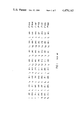
- FIG. 1 illustrates the standard T3 format.
- FIG. 1 is organized on seven lines, thus each line represents a different frame, the seven lines shown in FIG. 1 represent a single seven-frame multiframe.
- X represents an alarm service channel wherein in any multiframe the two X bits are identical.
- the P bits are parity information for parity taken over all information time slots in the preceding multiframe; conventionally, both P bits are identical.
- the M bits are multiframe alignment signals appearing, as shown in the fifth, sixth and seventh frames. Conventionally M 0 and M 1 are 0 and 1, respectively.
- the F bits are frame bits, which appear in a sequence as shown in FIG.
- Each frame provides for stuffing indicator bits C xy , where x identifies a frame and y is an integer in the range of 1-3. In any one frame, only one of two stuffing indicator words are allowed, either 000 or 111.
- the stuff time slot is the first data slot following F 1 after C i3 in the ith frame.
- the representation 84I represents 84 data bits.
- FIG. 1 can be said to represent a multiframe consisting of 56 85-bit digital words with each 85-bit digital word consisting of a single control bit and 84 data bits.
- FIG. 2 The particularized frame produced by the apparatus, and used in the method, of the present invention is shown in FIG. 2.
- each different frame is shown on four lines, those skilled in the art will understand of course that each frame is actually a time sequence which begins at the upper left, proceeds horizontally across to the end of the line, then drops down to the next line and begins at the left, and so forth.
- FIG. 2 also shows the seven different frames of each multiframe.
- the illustration in FIG. 2 is somewhat expanded relative to that of FIG. 1.
- the X, P, M 0 , M 1 , F 0 and F 1 positions have the same meaning as in FIG. 1.
- FIG. 2 indicates that it includes the X bit, a 4-bit audio nibble comprising bits A 1A through A 1D , and 80 bits consisting of 20 4-bit video samples (each sample including bits V 1 -V 4 ).
- the second 85-bit word includes a frame alignment bit F 1 and 21 4-bit video samples. It should be apparent from the format of FIG. 2 that every even word, that is the 28 85-bit words numbered 2-56 include 21 4-bit video samples and the first (control) bit is either F 1 or F 0 .
- the 28 odd 85-bit words each include 20 4-bit video samples, but for the most part the first 4-bit nibble is not a video sample.
- the bit positions A 1x and A 2x (where x is an alphabetic character from A-L, inclusive) represents two different audio channels.
- the 4-bit nibbles represented by the U bit positions are unused, the 4-bit nibble represented by the S bit positions are a single stuff opportunity per multiframe.
- the stuffing indicator bits are represented by some of the C bit positions, but in contrast to FIG. 1 which shows seven stuff opportunities, one for each frame, in FIG. 2 there is only one stuff opportunity per multiframe.
- the 4-bit nibble represented by the N bit positions is a further video sample.
- the unused bit positions carry time-consuming pulses, but do not represent meaningful information and are not employed, other than marking time, in the decoding process.
- the 4-bit nibble identified by the S bit positions is used for stuffing, if needed.
- the stuffing indicator word corresponds to the bit positions C xy (where x is 1-3 and y is 1-3). In any one multiframe, either all these bits are one, indicating the presence of stuffing, or all are zero, indicating the absence of stuffing.
- the bit positions identified by C xy (where x is 4 or 5 and y is 1-3, inclusive) are not used.
- the bit positions identified by C xy (where x is 6 or 7 and y is 1-3, inclusive) is a single bit frequency indicator appearing in six different locations in the multiframe.
- the frequency indicator indicates the measured value of f sc at the encoder (relative to the T3 rate) so the decoder can properly track and recreate the NTSC waveform.
- the apparatus to transmit the encoded video and auxiliary information in the T3 format is shown in FIG. 3.
- the 4-bit video samples which have been DPCM encoded via apparatus not shown is input to one terminal of a FIFO 10 on a 4-bit wide basis.
- a second input to the FIFO 10 is a horizontal sync signal.
- Both inputs to the FIFO 10 are written with the aid of a sampling clock which is related to the color subcarrier frequency f sc .
- a sampling clock is three times this subcarrier, i.e. typically 10.7 Mhz.
- the data path taken by the video samples proceeds from an output of the FIFO 10 to one input of a multiplexer 20.
- the multiplexer 20 Under control of a multiplexer control signal 21 from a sync detection and parity generation circuit 40, the multiplexer 20 accepts the 4-bit video samples, 4-bit sync and parity code words from the sync detection and parity generator 40 or 4-bit audio samples from a latch 50.
- the data multiplexer 20 produces a 4-bit wide XMIT data output, which is itself input to an overhead multiplexer 30.
- the other input to the overhead multiplexer 30 is frame and overhead bits from a frame and overhead generation circuit 70.
- the overhead multiplexer 30 accepts one or the other of its inputs in response to a multiplexer control signal 31 also derived from the frame and overhead generation circuit 70.
- the output of the multiplexer 30 is a serial stream at the T3 rate and in the T3 format which may, for example, be coupled through an amplifier 35 and output.
- a B3ZS encoder 80 accepts the T3 data and produces at an output bipolar T3 data for transmission purposes.
- the clock for reading the FIFO 10 is initially derived from a T3 clock which is input to a timing and control circuit 90.
- the timing and control circuit 90 produces an audio sampling clock and an audio nibble clock, both related to the T3 rate. These are used in the audio sampling equipment (not shown) which produces the audio data input to latch 50. Accordingly, the audio data is synchronous with the T3 clock.
- the timing and control circuit 90 produces a data clock 91, at 1/4 the T3 rate, or 11.184 MHz. This data clock 91 is input to the sync detection and parity generation circuit 40 which, in response thereto, couples a read clock 41 at 11.184 MHz to the FIFO 10.
- the T3 rate clock is also input to the frame and overhead generation circuit 70.
- This allows the production of the overhead multiplexer control signal 31 as well as the frame and overhead bits which provide one input to the overhead multiplexer 30.
- the frame and overhead generation circuit 70 also produces a multiframe signal 71 which is input to a frequency code generation circuit 60.
- the other input to the frequency code generation circuit is the sampling clock used to write the FIFO 10.
- the frequency code generation circuit 60 compares the periods of its two input signals.
- An output of the frequency code generation circuit 60 is a digital frequency code 61 which is input to the frame and overhead generation circuit 70 where it is used as a frequency indicator indicative of the frequency (f sc ), representing the sampling clock rate, and therefore the write clock rate for FIFO 10.
- audio data samples are coupled as an input to the latch 50.
- this audio data is accepted by the data multiplexer 20 for insertion into the serial 4-bit wide stream XMIT data.
- the sync detection and parity generation circuit 40 produces the data multiplexer control signal 21 and a sync and parity code word as referred to above. It receives the data clock 91 from the timing and control circuit 90 and from that fashions the read clock 41 to read the FIFO 10.
- the sync detection and parity generation circuit 40 is also responsive to a vertical sync signal from the video output as well as an indication that the FIFO 10 has read a horizontal sync signal. In response to the horizontal sync, the sync detection and parity generation circuit 40 interrupts the read clock 41 and provides the sync and parity code words to the data multiplexer 20 for insertion in the frame as shown in FIG. 2.
- the sync and parity words can be inserted into any video nibble.
- the read clock 41 is again enabled to continue reading FIFO 10.
- the T3 frame is composed of a time sequence of frame and other control bits dictated by the T3 format, video samples in the position specified in FIG. 2, a specified plurality of 4-bit nibbles representing the beginning of each horizontal line scan and the frequency code indicator produced by the frequency code generator 60.
- FIGS. 4-7 show, in more detail, the sync detection and parity generation circuit 40 as well as the associated data multiplexer 20, audio data latch 50 and timing and control circuit 90.
- FIGS. 8-10 show relevant waveforms.
- FIG. 8 A timing diagram is shown in FIG. 8 relating the video sampling clock to the video difference code and horizontal sync.
- the period T is 93.5 nanoseconds
- the data setup time t SU is 30 nanoseconds minimum
- the data hold time t HD is 30 nanoseconds minimum.
- FIG. 8 in indicating the timing of the horizontal sync pulse relative to the video sampling clock should not be taken as implying that a horizontal sync pulse is coincident with each video sampling clock, rather the horizontal sync pulse is produced at the beginning of each horizontal line scan.
- the video difference samples and the horizontal sync pulse are shifted out of the FIFO's 101 and 102 by the shift out clocks SOA and SOB. Both these shift out clocks are 11.184 MHz burst rate derivatives of the T3 clock.
- the shift out clocks' derivation is shown in FIG. 5 and will be discussed hereinafter. Accordingly, the FIFO's 101, 102 provide the function of a buffer.
- the output conductors of FIFO's 101 and 102 carry the video difference codes to the input of parity generator 104.
- the video difference codes, as read out from FIFO 101 or FIFO 102 are latched by the 11.184 MHz clock into a latch 105.
- the output of the latch 105 comprises a 4-bit wide tristate data bus (DB0-DB3) and the latch 105 is controlled by the signal DISABLE VIDEO or ENABLE VIDEO/Enable Sync & Parity (which is abbreviated EV/ES & P in FIG. 4). The production of both signals is described hereinafter.
- Audio samples are latched into a latch 106 via a nibble clock also derived from the timing control 90.
- the timing control 90 produces an audio sampling clock and an audio nibble clock; the timing is shown in FIG. 9.
- the sampled audio produces audio data; and as is shown in FIG. 9, the clocks provide for three 4-bit nibbles for each of two channels.
- the output of latch 106 is tristated onto the bus under control of the signal ENABLE AUDIO. Since the signals DISABLE VIDEO and ENABLE AUDIO are mutually exclusive, only one of the latches 105 or 106 places an output on the tristate data bus at any one time.
- Horizontal sync and parity is derived from the latch 107 which is clocked by the parity/sync clock, the production of which is shown in FIG. 5.
- the timing for the operation is shown in FIG. 10.
- the first two lines on FIG. 10 illustrate the 11.184 MHz derivative of the T3 clock and the second line illustrates one of the shift out clocks (SOA).
- the third line of FIG. 10 shows horizontal sync read out of either FIFO 101 or FIFO 102. When present, this pulse is latched, by the parity/sync clock, into the hex "D" flip-flop 108. At the Q5 output, the rising edge of the signal clocks flip-flop 109 producing the SYNC DETECT pulse; which is shown in the fifth line in FIG. 10. SYNC DETECT/LATCH PARITY is used to latch and then reset (via flip-flops 111, 112), the parity on the difference code.
- the opposite phase LATCH PARITY (output of the inverter 113) resets parity (flip-flop 111) and is latched by the 11 MHz clock (see FIG. 5) in flip-flop 116.
- the output of flip-flop 116 is STOP VIDEO, which is gated with the 11 MHz clock (gate 117) to stop the shift out clocks produced by flip-flop 118 is the absence of STOP VIDEO.
- the SYNC DETECT (LATCH PARITY) pulse is reclocked (in the zero stage) by the PARITY/SYNC CLOCK in the flip-flop 108 and the result, EV/ES & P ENABLE VIDEO/ENABLE SYNC AND PARITY) at the Q0 output (shown in line 6 of FIG. 10) is used to disable latch 105 and enable (via inverter 114) the output of the parity/sync latch 107.
- the output of latch 107 is tristated onto the common data bus (DB0-DB3).
- line 10 the sync detect results in EV/ES & P after a short delay.
- EV/ES & P is present for a total of four nibble times.
- three 4-bit nibbles, each 1's, are output from latch 107.
- the multiplexer 110 output Y A provides a single bit for each nibble and Y B provides the other three bits for each nibble.
- another 4-bit nibble is again put on the bus, however the makeup of this depends on the condition of S 1 . If S 1 is in a state indicating the presence of vertical sync, then the first three bits are all 1 and vice versa.
- the last bit is a parity bit from flip-flop 112.
- the T3 rate clock causes two counters 120 and 121 to count.
- the counters are arranged to divide the T3 rate clock by 85.
- One output produces the 11.184 MHz clock.
- the counters also produce a pulse, FRAME, which causes two additional counters 122 and 123 to count. These are arranged to divide the pulse FRAME by 56.
- the outputs of counters 122, 123 are the address lines of two 256 by 4 ROMs 124 which store multi-frame format data to generate necessary control signals.
- the output of the ROMs 124 is coupled to a hex flip-flop 125, one output of which is latched (by FRAME) into a flip-flop 126.
- flip-flop 126 The true output of flip-flop 126 is latched by an 11.184 MHz clock in a latch 127.
- DISABLE VIDEO and ENABLE AUDIO are the outputs of latch 127.
- DISABLE VIDEO disables the outputs of the video latch 105 and the parity/sync latch 107 when audio data is to be put on the data bus.
- ENABLE AUDIO is used to enable the output of the audio latch 106 and stops the shift out clocks via gate 128 (FIG. 5).
- the output of flip-flop 127 can be controlled to disable the video and enable audio at the appropriate times in the frame.
- the ROM 124 also stores other signals identifying other overhead locations in the frame. Specifically, the location of F, M, P, X, U and N (see FIG. 2) are stored in ROM 124. When read out of ROM 124, these are used to set two positions of the hex flip-flop 125 which produce the MUX select signals, also shown in FIG. 6.
- FIG. 5 also illustrates generation of the signal FREQ CODE.
- This is a digital signal representing the video clock rate.
- the video sampling clock is used to clock a quad flip-flop 141 with its outputs of one stage connected to inputs of the succeeding stage; the video sampling clock is also used to clock flip-flop 142 via exclusive OR gate 145. Accordingly, the flip-flop 142 provides for dividing the video sampling clock in half. At every multiframe, the output of flip-flop 142 is latched in flip-flop 143; the multiframe start input at stage D 0 is output of stage Q1 to clock flip-flop 143. Every multiframe, the flip-flop 142 is reset via NAND gate 144.
- the frequency code output is a single bit indicating a relation between the video sampling clock and the multiframe start.
- the frequency code output of flip-flop 143 provides one input to the multiplexer 130 (FIG. 7), another input to the multiplexer 130 corresponds to parity information coupled from parity generator 133 through flip-flop 135.
- the control signals for multiplexer 130 are provided by MUX select, i.e. from hex flip-flop 125 (FIG. 6).
- MUX select i.e. from hex flip-flop 125 (FIG. 6).
- LOAD SR pulse is produced via flip-flop 146. This is clocked with the T3 clock, and is set by the output of NAND gate 148, one of whose inputs is provided by the 4-bit counter 120, and the other of whose inputs is provided via NOR gate 147 from another output of the 4-bit counter 120.
- the LOAD SR signal is used to load shift register 131 (see FIG. 7).
- the information for this parallel loading of shift register 131 is provided by a buffer 132 which receives its input in turn from the 4-bit wide tristate data bus DB0-DB3.
- the inputs to the buffer 131 are coupled in parallel to the parity generator 133 to generate the parity information referred to above.
- the shift register 131 can also be serially loaded from the multiplexer 130 in a manner well-known to those skilled in the art.
- the MUX SELECT signals select frequency code parity information, or fixed data from the other multiplexer inputs, for shifting through the multiplexer 130 to the shift register 131 and out on the line labelled SERIAL DATA. It should be apparent how the ROM data stores a frame plan to generate appropriate MUX select signals to produce insertion of the appropriate inputs into the multiframe.
- the ROM 124 is also addressed by alarm and stuffing information.
- An alarm signal is generated (by equipment not illustrated), and its presence (or absence) produces the MUX SELECT signals to insert bits indicating the presence (or absence) of an alarm condition.
- the necessity for stuffing is determined. If stuffing is required, the signal disable video is inhibited. If stuffing is not required, the signal is not inhibited and instead the MUX SELECT provides a fixed bit pattern in the unused stuff opportunity. The stuffing requirement is also used via ROM 124 to generate the appropriate stuffing indicator bits in the same fashion.
- the interface described herein provides for a standard T3 format in which the information bearing signals consist of 4-bit nibbles of DPCM video and 4-bit audio nibbles.
- the clock reading out the 4-bit video DPCM nibbles is inhibited and a predetermined sequence (depending on whether or not horizontal or vertical sync is occurred) is inserted onto the data bus in place of a video nibble.
- a predetermined sequence (depending on whether or not horizontal or vertical sync is occurred) is inserted onto the data bus in place of a video nibble.
- parity, frequency code information or other data is inserted in a predetermined format.
- the multiplexer 20 (FIG. 3) which multiplexes, video samples, audio samples, sync digital codes and parity corresonds to the latches 105-107 and the attached tri-state bus DB0-DB3.
- the multiplexer 30 which multiplexes the output of multiplexer 20 with frame and overhead bits corresponds to the multiplexer 130, shift register 131 and buffer 132 (all in FIG. 7). The use of the shift register allows concurrent multiplexing and serializes the input from the tri-state bus DB0-DB3.
Abstract
Description
Claims (12)
Priority Applications (2)
| Application Number | Priority Date | Filing Date | Title |
|---|---|---|---|
| US06/379,382 US4479142A (en) | 1982-05-17 | 1982-05-17 | Interface apparatus and method for asynchronous encoding of digital television |
| CA000422179A CA1189953A (en) | 1982-05-17 | 1983-02-23 | Interface apparatus and method for asynchronous encoding of digital television |
Applications Claiming Priority (1)
| Application Number | Priority Date | Filing Date | Title |
|---|---|---|---|
| US06/379,382 US4479142A (en) | 1982-05-17 | 1982-05-17 | Interface apparatus and method for asynchronous encoding of digital television |
Publications (1)
| Publication Number | Publication Date |
|---|---|
| US4479142A true US4479142A (en) | 1984-10-23 |
Family
ID=23497010
Family Applications (1)
| Application Number | Title | Priority Date | Filing Date |
|---|---|---|---|
| US06/379,382 Expired - Lifetime US4479142A (en) | 1982-05-17 | 1982-05-17 | Interface apparatus and method for asynchronous encoding of digital television |
Country Status (2)
| Country | Link |
|---|---|
| US (1) | US4479142A (en) |
| CA (1) | CA1189953A (en) |
Cited By (47)
| Publication number | Priority date | Publication date | Assignee | Title |
|---|---|---|---|---|
| WO1985003184A1 (en) * | 1984-01-03 | 1985-07-18 | American Telephone & Telegraph Company | Technique for the transmission of video and audio signals over a digital transmission system |
| US4607364A (en) * | 1983-11-08 | 1986-08-19 | Jeffrey Neumann | Multimode data communication system |
| US4807031A (en) * | 1987-10-20 | 1989-02-21 | Interactive Systems, Incorporated | Interactive video method and apparatus |
| US4870479A (en) * | 1988-05-02 | 1989-09-26 | Dubner Computer Systems, Inc. | Video graphics memory storage reduction technique |
| US5081619A (en) * | 1988-11-11 | 1992-01-14 | Hitachi, Ltd. | Digital signal multiplex communication system having signal path monitoring function |
| US5161191A (en) * | 1990-11-27 | 1992-11-03 | Gupta Shanti S | Encryption system for time division multiplexed networks |
| US5204882A (en) * | 1990-12-14 | 1993-04-20 | Bell Communications Research, Inc. | Service clock recovery for variable bit rate services |
| US5387945A (en) * | 1988-07-13 | 1995-02-07 | Seiko Epson Corporation | Video multiplexing system for superimposition of scalable video streams upon a background video data stream |
| US5655945A (en) * | 1992-10-19 | 1997-08-12 | Microsoft Corporation | Video and radio controlled moving and talking device |
| US5929933A (en) * | 1988-07-13 | 1999-07-27 | Seiko Epson Corporation | Video multiplexing system for superimposition of scalable video data streams upon a background video data stream |
| US20020042923A1 (en) * | 1992-12-09 | 2002-04-11 | Asmussen Michael L. | Video and digital multimedia aggregator content suggestion engine |
| US6618095B1 (en) * | 1998-12-07 | 2003-09-09 | Matsushita Electric Industrial Co., Ltd. | Serial digital interface system transmission/reception method and device therefor |
| US20040104755A1 (en) * | 2002-01-31 | 2004-06-03 | Noriyuki Suzuki | SDI signal discriminating apparatus |
| US7096487B1 (en) * | 1999-10-27 | 2006-08-22 | Sedna Patent Services, Llc | Apparatus and method for combining realtime and non-realtime encoded content |
| US20070044007A1 (en) * | 2005-08-17 | 2007-02-22 | International Business Machines Corporation | Method and apparatus for providing error correction capability to longitudinal position data |
| US20070286246A1 (en) * | 2003-05-01 | 2007-12-13 | Genesis Microchip Inc. | Multimedia interface |
| US20080246711A1 (en) * | 2003-09-18 | 2008-10-09 | Genesis Microchip Inc. | Using packet transfer for driving lcd panel driver electronics |
| US20080288263A1 (en) * | 2005-09-14 | 2008-11-20 | Lg Electronics, Inc. | Method and Apparatus for Encoding/Decoding |
| US7464394B1 (en) | 1999-07-22 | 2008-12-09 | Sedna Patent Services, Llc | Music interface for media-rich interactive program guide |
| US20090128698A1 (en) * | 2007-11-21 | 2009-05-21 | Yoshinori Okajima | Audio synchronizer for digital television broadcast |
| US7733915B2 (en) | 2003-05-01 | 2010-06-08 | Genesis Microchip Inc. | Minimizing buffer requirements in a digital video system |
| US20100146554A1 (en) * | 1999-04-15 | 2010-06-10 | Comcast Ip Holdings I, Llc | Temporal Slice Persistence Method and Apparatus for Delivery of Interactive Program Guide |
| US7800623B2 (en) | 2003-09-18 | 2010-09-21 | Genesis Microchip Inc. | Bypassing pixel clock generation and CRTC circuits in a graphics controller chip |
| US7839860B2 (en) | 2003-05-01 | 2010-11-23 | Genesis Microchip Inc. | Packet based video display interface |
| US20110022961A1 (en) * | 1998-07-23 | 2011-01-27 | Comcast Ip Holdings I, Llc | Interactive User Interface |
| US8032906B2 (en) | 1999-10-27 | 2011-10-04 | Comcast Ip Holdings I, Llc | Method and system for providing a program guide and multiple video streams using slice-based encoding |
| US8059673B2 (en) | 2003-05-01 | 2011-11-15 | Genesis Microchip Inc. | Dynamic resource re-allocation in a packet based video display interface |
| US8156238B2 (en) | 2009-05-13 | 2012-04-10 | Stmicroelectronics, Inc. | Wireless multimedia transport method and apparatus |
| US8204076B2 (en) | 2003-05-01 | 2012-06-19 | Genesis Microchip Inc. | Compact packet based multimedia interface |
| US8291207B2 (en) | 2009-05-18 | 2012-10-16 | Stmicroelectronics, Inc. | Frequency and symbol locking using signal generated clock frequency and symbol identification |
| US8370554B2 (en) | 2009-05-18 | 2013-02-05 | Stmicroelectronics, Inc. | Operation of video source and sink with hot plug detection not asserted |
| US8385544B2 (en) | 2003-09-26 | 2013-02-26 | Genesis Microchip, Inc. | Packet based high definition high-bandwidth digital content protection |
| US8429440B2 (en) | 2009-05-13 | 2013-04-23 | Stmicroelectronics, Inc. | Flat panel display driver method and system |
| US8468285B2 (en) | 2009-05-18 | 2013-06-18 | Stmicroelectronics, Inc. | Operation of video source and sink with toggled hot plug detection |
| US8578419B2 (en) | 1999-04-15 | 2013-11-05 | Comcast Ip Holdings I, Llc | Server-centric customized interactive program guide in an interactive television environment |
| US8582452B2 (en) | 2009-05-18 | 2013-11-12 | Stmicroelectronics, Inc. | Data link configuration by a receiver in the absence of link training data |
| US8671234B2 (en) | 2010-05-27 | 2014-03-11 | Stmicroelectronics, Inc. | Level shifting cable adaptor and chip system for use with dual-mode multi-media device |
| US8739218B2 (en) | 1998-07-23 | 2014-05-27 | Comcast Ip Holdings I, Llc | Data structure and methods for providing an interactive program guide |
| US8760461B2 (en) | 2009-05-13 | 2014-06-24 | Stmicroelectronics, Inc. | Device, system, and method for wide gamut color space support |
| US8860888B2 (en) | 2009-05-13 | 2014-10-14 | Stmicroelectronics, Inc. | Method and apparatus for power saving during video blanking periods |
| US9154813B2 (en) | 2011-06-09 | 2015-10-06 | Comcast Cable Communications, Llc | Multiple video content in a composite video stream |
| US20170134040A1 (en) * | 2014-06-30 | 2017-05-11 | Indice Semiconductor Inc. | Asynchronous electrical circuitry techniques for producing stationary carrier signal to encode input signal amplitude into output signal time-sequence information |
| US9813641B2 (en) | 2000-06-19 | 2017-11-07 | Comcast Ip Holdings I, Llc | Method and apparatus for targeting of interactive virtual objects |
| US9924234B2 (en) | 1998-07-23 | 2018-03-20 | Comcast Ip Holdings I, Llc | Data structure and methods for providing an interactive program |
| US10140433B2 (en) | 2001-08-03 | 2018-11-27 | Comcast Ip Holdings I, Llc | Video and digital multimedia aggregator |
| US10349096B2 (en) | 2001-08-03 | 2019-07-09 | Comcast Ip Holdings I, Llc | Video and digital multimedia aggregator content coding and formatting |
| US10681399B2 (en) * | 2002-10-23 | 2020-06-09 | The Nielsen Company (Us), Llc | Digital data insertion apparatus and methods for use with compressed audio/video data |
Citations (1)
| Publication number | Priority date | Publication date | Assignee | Title |
|---|---|---|---|---|
| US4122477A (en) * | 1977-01-28 | 1978-10-24 | Ampex Corporation | Method and apparatus for inserting synchronizing words in a digitalized television signal data stream |
-
1982
- 1982-05-17 US US06/379,382 patent/US4479142A/en not_active Expired - Lifetime
-
1983
- 1983-02-23 CA CA000422179A patent/CA1189953A/en not_active Expired
Patent Citations (1)
| Publication number | Priority date | Publication date | Assignee | Title |
|---|---|---|---|---|
| US4122477A (en) * | 1977-01-28 | 1978-10-24 | Ampex Corporation | Method and apparatus for inserting synchronizing words in a digitalized television signal data stream |
Cited By (66)
| Publication number | Priority date | Publication date | Assignee | Title |
|---|---|---|---|---|
| US4607364A (en) * | 1983-11-08 | 1986-08-19 | Jeffrey Neumann | Multimode data communication system |
| US4544950A (en) * | 1984-01-03 | 1985-10-01 | At&T Bell Laboratories | Technique for the transmission of video and audio signals over a digital transmission system |
| WO1985003184A1 (en) * | 1984-01-03 | 1985-07-18 | American Telephone & Telegraph Company | Technique for the transmission of video and audio signals over a digital transmission system |
| US4807031A (en) * | 1987-10-20 | 1989-02-21 | Interactive Systems, Incorporated | Interactive video method and apparatus |
| US4870479A (en) * | 1988-05-02 | 1989-09-26 | Dubner Computer Systems, Inc. | Video graphics memory storage reduction technique |
| US5929933A (en) * | 1988-07-13 | 1999-07-27 | Seiko Epson Corporation | Video multiplexing system for superimposition of scalable video data streams upon a background video data stream |
| USRE37879E1 (en) | 1988-07-13 | 2002-10-15 | Seiko Epson Corporation | Image control device for use in a video multiplexing system for superimposition of scalable video data streams upon a background video data stream |
| US5387945A (en) * | 1988-07-13 | 1995-02-07 | Seiko Epson Corporation | Video multiplexing system for superimposition of scalable video streams upon a background video data stream |
| US5929870A (en) * | 1988-07-13 | 1999-07-27 | Seiko Epson Corporation | Video multiplexing system for superimposition of scalable video data streams upon a background video data stream |
| US5793439A (en) * | 1988-07-13 | 1998-08-11 | Seiko Epson Corporation | Image control device for use in a video multiplexing system for superimposition of scalable video data streams upon a background video data stream |
| US5081619A (en) * | 1988-11-11 | 1992-01-14 | Hitachi, Ltd. | Digital signal multiplex communication system having signal path monitoring function |
| US5161191A (en) * | 1990-11-27 | 1992-11-03 | Gupta Shanti S | Encryption system for time division multiplexed networks |
| US5204882A (en) * | 1990-12-14 | 1993-04-20 | Bell Communications Research, Inc. | Service clock recovery for variable bit rate services |
| US5655945A (en) * | 1992-10-19 | 1997-08-12 | Microsoft Corporation | Video and radio controlled moving and talking device |
| US20020042923A1 (en) * | 1992-12-09 | 2002-04-11 | Asmussen Michael L. | Video and digital multimedia aggregator content suggestion engine |
| US9286294B2 (en) | 1992-12-09 | 2016-03-15 | Comcast Ip Holdings I, Llc | Video and digital multimedia aggregator content suggestion engine |
| US8739218B2 (en) | 1998-07-23 | 2014-05-27 | Comcast Ip Holdings I, Llc | Data structure and methods for providing an interactive program guide |
| US9924234B2 (en) | 1998-07-23 | 2018-03-20 | Comcast Ip Holdings I, Llc | Data structure and methods for providing an interactive program |
| US9674586B2 (en) | 1998-07-23 | 2017-06-06 | Comcast Ip Holdings I, Llc | Data structure and methods for providing an interactive program guide |
| US20110022961A1 (en) * | 1998-07-23 | 2011-01-27 | Comcast Ip Holdings I, Llc | Interactive User Interface |
| US8522277B2 (en) | 1998-07-23 | 2013-08-27 | Comcast Ip Holdings I, Llc | Interactive user interface |
| US6618095B1 (en) * | 1998-12-07 | 2003-09-09 | Matsushita Electric Industrial Co., Ltd. | Serial digital interface system transmission/reception method and device therefor |
| US8578419B2 (en) | 1999-04-15 | 2013-11-05 | Comcast Ip Holdings I, Llc | Server-centric customized interactive program guide in an interactive television environment |
| US9042446B2 (en) | 1999-04-15 | 2015-05-26 | Comcast Ip Holdings I, Llc | Temporal slice persistence method and apparatus for delivery of interactive program guide |
| US9456241B2 (en) | 1999-04-15 | 2016-09-27 | Comcast Ip Holdings I, Llc | Server-centric customized interactive program guide in an interactive television environment |
| US20100146554A1 (en) * | 1999-04-15 | 2010-06-10 | Comcast Ip Holdings I, Llc | Temporal Slice Persistence Method and Apparatus for Delivery of Interactive Program Guide |
| US7464394B1 (en) | 1999-07-22 | 2008-12-09 | Sedna Patent Services, Llc | Music interface for media-rich interactive program guide |
| US8032906B2 (en) | 1999-10-27 | 2011-10-04 | Comcast Ip Holdings I, Llc | Method and system for providing a program guide and multiple video streams using slice-based encoding |
| US7096487B1 (en) * | 1999-10-27 | 2006-08-22 | Sedna Patent Services, Llc | Apparatus and method for combining realtime and non-realtime encoded content |
| US8930998B2 (en) | 1999-10-27 | 2015-01-06 | Comcast Ip Holdings I, Llc | Method and system for providing a program guide and multiple video streams using slice-based encoding |
| US20100296574A1 (en) * | 1999-10-27 | 2010-11-25 | Comcast Ip Holdings I, Llc | Apparatus and method for combining realtime and non-realtime encoded content |
| US9264711B2 (en) | 1999-10-27 | 2016-02-16 | Comcast Ip Holdings I, Llc | Apparatus and method for combining realtime and non-realtime encoded content |
| US8661465B2 (en) | 1999-10-27 | 2014-02-25 | Comcast Ip Holdings I, Llc | Apparatus and method for combining realtime and non-realtime encoded content |
| US7810116B2 (en) | 1999-10-27 | 2010-10-05 | Comcast Ip Holdings I, Llc | Apparatus and method for combining realtime and non-realtime encoded content |
| US9813641B2 (en) | 2000-06-19 | 2017-11-07 | Comcast Ip Holdings I, Llc | Method and apparatus for targeting of interactive virtual objects |
| US10140433B2 (en) | 2001-08-03 | 2018-11-27 | Comcast Ip Holdings I, Llc | Video and digital multimedia aggregator |
| US10349096B2 (en) | 2001-08-03 | 2019-07-09 | Comcast Ip Holdings I, Llc | Video and digital multimedia aggregator content coding and formatting |
| US20040104755A1 (en) * | 2002-01-31 | 2004-06-03 | Noriyuki Suzuki | SDI signal discriminating apparatus |
| US10681399B2 (en) * | 2002-10-23 | 2020-06-09 | The Nielsen Company (Us), Llc | Digital data insertion apparatus and methods for use with compressed audio/video data |
| US11223858B2 (en) | 2002-10-23 | 2022-01-11 | The Nielsen Company (Us), Llc | Digital data insertion apparatus and methods for use with compressed audio/video data |
| US8059673B2 (en) | 2003-05-01 | 2011-11-15 | Genesis Microchip Inc. | Dynamic resource re-allocation in a packet based video display interface |
| US8204076B2 (en) | 2003-05-01 | 2012-06-19 | Genesis Microchip Inc. | Compact packet based multimedia interface |
| US7733915B2 (en) | 2003-05-01 | 2010-06-08 | Genesis Microchip Inc. | Minimizing buffer requirements in a digital video system |
| US8068485B2 (en) | 2003-05-01 | 2011-11-29 | Genesis Microchip Inc. | Multimedia interface |
| US20070286246A1 (en) * | 2003-05-01 | 2007-12-13 | Genesis Microchip Inc. | Multimedia interface |
| US7839860B2 (en) | 2003-05-01 | 2010-11-23 | Genesis Microchip Inc. | Packet based video display interface |
| US20080246711A1 (en) * | 2003-09-18 | 2008-10-09 | Genesis Microchip Inc. | Using packet transfer for driving lcd panel driver electronics |
| US7800623B2 (en) | 2003-09-18 | 2010-09-21 | Genesis Microchip Inc. | Bypassing pixel clock generation and CRTC circuits in a graphics controller chip |
| US8385544B2 (en) | 2003-09-26 | 2013-02-26 | Genesis Microchip, Inc. | Packet based high definition high-bandwidth digital content protection |
| US20070044007A1 (en) * | 2005-08-17 | 2007-02-22 | International Business Machines Corporation | Method and apparatus for providing error correction capability to longitudinal position data |
| US7421640B2 (en) * | 2005-08-17 | 2008-09-02 | International Business Machines Corporation | Method and apparatus for providing error correction capability to longitudinal position data |
| US20080288263A1 (en) * | 2005-09-14 | 2008-11-20 | Lg Electronics, Inc. | Method and Apparatus for Encoding/Decoding |
| US20090128698A1 (en) * | 2007-11-21 | 2009-05-21 | Yoshinori Okajima | Audio synchronizer for digital television broadcast |
| US8156238B2 (en) | 2009-05-13 | 2012-04-10 | Stmicroelectronics, Inc. | Wireless multimedia transport method and apparatus |
| US8860888B2 (en) | 2009-05-13 | 2014-10-14 | Stmicroelectronics, Inc. | Method and apparatus for power saving during video blanking periods |
| US8788716B2 (en) | 2009-05-13 | 2014-07-22 | Stmicroelectronics, Inc. | Wireless multimedia transport method and apparatus |
| US8760461B2 (en) | 2009-05-13 | 2014-06-24 | Stmicroelectronics, Inc. | Device, system, and method for wide gamut color space support |
| US8429440B2 (en) | 2009-05-13 | 2013-04-23 | Stmicroelectronics, Inc. | Flat panel display driver method and system |
| US8291207B2 (en) | 2009-05-18 | 2012-10-16 | Stmicroelectronics, Inc. | Frequency and symbol locking using signal generated clock frequency and symbol identification |
| US8582452B2 (en) | 2009-05-18 | 2013-11-12 | Stmicroelectronics, Inc. | Data link configuration by a receiver in the absence of link training data |
| US8468285B2 (en) | 2009-05-18 | 2013-06-18 | Stmicroelectronics, Inc. | Operation of video source and sink with toggled hot plug detection |
| US8370554B2 (en) | 2009-05-18 | 2013-02-05 | Stmicroelectronics, Inc. | Operation of video source and sink with hot plug detection not asserted |
| US8671234B2 (en) | 2010-05-27 | 2014-03-11 | Stmicroelectronics, Inc. | Level shifting cable adaptor and chip system for use with dual-mode multi-media device |
| US9154813B2 (en) | 2011-06-09 | 2015-10-06 | Comcast Cable Communications, Llc | Multiple video content in a composite video stream |
| US20170134040A1 (en) * | 2014-06-30 | 2017-05-11 | Indice Semiconductor Inc. | Asynchronous electrical circuitry techniques for producing stationary carrier signal to encode input signal amplitude into output signal time-sequence information |
| US9813077B2 (en) * | 2014-06-30 | 2017-11-07 | Indice Semiconductor Inc. | Asynchronous electrical circuitry techniques for producing stationary carrier signal to encode input signal amplitude into output signal time-sequence information |
Also Published As
| Publication number | Publication date |
|---|---|
| CA1189953A (en) | 1985-07-02 |
Similar Documents
| Publication | Publication Date | Title |
|---|---|---|
| US4479142A (en) | Interface apparatus and method for asynchronous encoding of digital television | |
| US5687356A (en) | Hub and interface for isochronous token ring | |
| US4397020A (en) | Error monitoring in digital transmission systems | |
| US5189410A (en) | Digital cross connect system | |
| US4928275A (en) | Synchronization of asynchronous data signals | |
| USRE33900E (en) | Error monitoring in digital transmission systems | |
| US4383322A (en) | Combined use of PN sequence for data scrambling and frame synchronization in digital communication systems | |
| US4587514A (en) | Interface method and apparatus | |
| KR100360134B1 (en) | Signal processing system | |
| CA1105586A (en) | Digital data transmission arrangement | |
| CA1151260A (en) | Digital data transmission system | |
| JPH0710058B2 (en) | Advanced digital communication system with multiplexer and demultiplexer | |
| US4398290A (en) | Process and apparatus for digital data communication using packet switching | |
| GB1481849A (en) | Digital code transmission systems | |
| US4481648A (en) | Method and system for producing a synchronous signal from _cyclic-redundancy-coded digital data blocks | |
| CA1187169A (en) | Video/audio simultaneous transmission system | |
| US4713692A (en) | Method and apparatus for deriving frame interval signals | |
| US5006936A (en) | Method and system for high density analog data storage retrieval, and transmission | |
| US5504752A (en) | Pulse stuffing synchronization control system | |
| US4665444A (en) | Circuit for reproducing video signals | |
| US4203003A (en) | Frame search control for digital transmission system | |
| US4442520A (en) | Signal error detecting | |
| CA1074029A (en) | Framing circuit for digital signals using evenly spaced alternating framing bits | |
| EP0299265A2 (en) | Receiver synchronization in encoder/decoder | |
| CA1291832C (en) | Higher order digital transmission system including a multiplexer and a demultiplexer |
Legal Events
| Date | Code | Title | Description |
|---|---|---|---|
| AS | Assignment |
Owner name: DIGITAL COMMUNICATIONS CORPORATION, 11717 EXPLORAT Free format text: ASSIGNMENT OF ASSIGNORS INTEREST.;ASSIGNORS:BUSCHMAN, BOB D.;MUTH, GLENN D.;O'CONNELL, RONALD T.;REEL/FRAME:004003/0149 Effective date: 19820504 Owner name: DIGITAL COMMUNICATIONS CORPORATION, A CORP. OF DEL Free format text: ASSIGNMENT OF ASSIGNORS INTEREST;ASSIGNORS:BUSCHMAN, BOB D.;MUTH, GLENN D.;O'CONNELL, RONALD T.;REEL/FRAME:004003/0149 Effective date: 19820504 |
|
| AS | Assignment |
Owner name: M/A-COM DCC, INC. Free format text: CHANGE OF NAME;ASSIGNOR:DIGITAL COMMUNICATIONS CORPORATION;REEL/FRAME:003997/0789 Effective date: 19820426 |
|
| STCF | Information on status: patent grant |
Free format text: PATENTED CASE |
|
| AS | Assignment |
Owner name: M/A-COM TELECOMMUNICATIONS, INC., Free format text: CHANGE OF NAME;ASSIGNOR:M/A-COM DCC, INC.,;REEL/FRAME:004537/0868 Effective date: 19851216 |
|
| FEPP | Fee payment procedure |
Free format text: PAYOR NUMBER ASSIGNED (ORIGINAL EVENT CODE: ASPN); ENTITY STATUS OF PATENT OWNER: LARGE ENTITY |
|
| FPAY | Fee payment |
Year of fee payment: 4 |
|
| AS | Assignment |
Owner name: HUGHES NETWORK SYSTEMS, INC. Free format text: CHANGE OF NAME;ASSIGNOR:M/A-COM TELECOMMUNICATIONS, INC.,;REEL/FRAME:004827/0112 Effective date: 19870930 |
|
| FPAY | Fee payment |
Year of fee payment: 8 |
|
| FEPP | Fee payment procedure |
Free format text: PAYER NUMBER DE-ASSIGNED (ORIGINAL EVENT CODE: RMPN); ENTITY STATUS OF PATENT OWNER: LARGE ENTITY Free format text: PAYOR NUMBER ASSIGNED (ORIGINAL EVENT CODE: ASPN); ENTITY STATUS OF PATENT OWNER: LARGE ENTITY |
|
| FPAY | Fee payment |
Year of fee payment: 12 |
|
| AS | Assignment |
Owner name: HUGHES ELECTRONICS CORPORATION, CALIFORNIA Free format text: ASSIGNMENT OF ASSIGNORS INTEREST;ASSIGNOR:HE HOLDINGS INC., HUGHES ELECTRONICS, FORMERLY KNOWN AS HUGHES AIRCRAFT COMPANY;REEL/FRAME:009123/0473 Effective date: 19971216 |