US4489998A - Bussing connector system - Google Patents
Bussing connector system Download PDFInfo
- Publication number
- US4489998A US4489998A US06/437,997 US43799782A US4489998A US 4489998 A US4489998 A US 4489998A US 43799782 A US43799782 A US 43799782A US 4489998 A US4489998 A US 4489998A
- Authority
- US
- United States
- Prior art keywords
- pin
- bussing
- circuit board
- shroud
- header
- Prior art date
- Legal status (The legal status is an assumption and is not a legal conclusion. Google has not performed a legal analysis and makes no representation as to the accuracy of the status listed.)
- Expired - Fee Related
Links
Images


Classifications
-
- H—ELECTRICITY
- H01—ELECTRIC ELEMENTS
- H01R—ELECTRICALLY-CONDUCTIVE CONNECTIONS; STRUCTURAL ASSOCIATIONS OF A PLURALITY OF MUTUALLY-INSULATED ELECTRICAL CONNECTING ELEMENTS; COUPLING DEVICES; CURRENT COLLECTORS
- H01R31/00—Coupling parts supported only by co-operation with counterpart
- H01R31/06—Intermediate parts for linking two coupling parts, e.g. adapter
-
- H—ELECTRICITY
- H01—ELECTRIC ELEMENTS
- H01R—ELECTRICALLY-CONDUCTIVE CONNECTIONS; STRUCTURAL ASSOCIATIONS OF A PLURALITY OF MUTUALLY-INSULATED ELECTRICAL CONNECTING ELEMENTS; COUPLING DEVICES; CURRENT COLLECTORS
- H01R12/00—Structural associations of a plurality of mutually-insulated electrical connecting elements, specially adapted for printed circuits, e.g. printed circuit boards [PCB], flat or ribbon cables, or like generally planar structures, e.g. terminal strips, terminal blocks; Coupling devices specially adapted for printed circuits, flat or ribbon cables, or like generally planar structures; Terminals specially adapted for contact with, or insertion into, printed circuits, flat or ribbon cables, or like generally planar structures
- H01R12/70—Coupling devices
- H01R12/71—Coupling devices for rigid printing circuits or like structures
- H01R12/712—Coupling devices for rigid printing circuits or like structures co-operating with the surface of the printed circuit or with a coupling device exclusively provided on the surface of the printed circuit
- H01R12/716—Coupling device provided on the PCB
- H01R12/718—Contact members provided on the PCB without an insulating housing
Definitions
- the present invention relates to a bussing connector system for providing a pluggable interconnect between conductive planes of adjacent pairs of parallel, spaced circuit boards.
- U.S. Pat. Nos. 3,404,367 and 3,634,816 both of which show a mother circuit board having a plurality of connector members attached thereto and the like plurality of daughter boards each having an edge connector received in a respective one of the mother circuit board connectors.
- U.S. Pat. No. 4,133,592 shows a connector for electrically and mechanically joining a plurality of circuit boards in a stack. This arrangement has a clear disadvantage in that the boards towards the middle of the stack are not readily accessible. Such arrangements are not readily adaptable and have the obvious disadvantage in that they must initially be designed into a system and then are rather fixed in configuration. They are, generally, rather expensive to install and maintain.
- the present invention pertains to a connector system which can be used to selectively connect any number of pairs of adjacent parallel spaced circuit boards.
- the subject connector system includes a bussing connector for each pair of circuit boards and a connector assembly mounted on each circuit board.
- Each bussing connector has a housing of rigid insulative material with a plurality of parallel spaced profiled slots. Each slot includes a groove on each opposite face of the connector extending away from a mating face in parallel spaced fashion.
- the bussing connector has a plurality of receptacle terminals, each mounted in a respective slot in the housing and each terminal having a cross bar portion and a pair of parallel spaced contact legs which lie in respective grooves.
- the connector assembly on each circuit board includes a pin header and a pin shroud mounted on opposite sides of a mating edge portion of each circuit board.
- Each header and each shroud have a plurality of terminal passages extending therethrough, each aligned with a respective conductive aperture in the circuit board.
- a plurality of pin terminals extend through the respective passages and conductive aperture of the circuit board to project from both oppositely directed mating faces of the header and shroud.
- the bussing connector terminals engage the pin terminals extending from the mating face of a pin header of a first circuit board and the pin terminals extending from the shroud of a second circuit board so that the circuits of the first and second boards are bussed together.
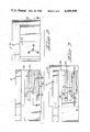
- FIG. 1 is an exploded perspective view of the subject connector system according to the present invention
- FIG. 2 is an elevation taken along line 2--2 of FIG. 4 showing an end portion of the subject connector system according to the present invention in an unmated condition;
- FIG. 3 is a view similar to FIG. 2 showing the subject connector system in the mated condition
- FIG. 4 is a section through the subject connector system in the unmated condition
- FIG. 5 is a perspective view of a bussing terminal of the type used in the present invention.
- FIG. 6 is a perspective view of a pin terminal of the type used in the present invention.
- FIG. 7 is a perspective view of the connector members of the subject connector system exploded from an edge portion of a circuit board
- FIG. 8 is a side elevation schematically illustrating the operation of the present invention.
- FIG. 9 is a perspective view of an alternate bussing connector for use in the present invention.
- FIG. 10 is a perspective view of a further alternate embodiment of a bussing connector for the subject invention.
- FIG. 11 is a perspective view of the subject invention in a backplane mounting configuration.
- the subject bussing system 20 is formed by a bussing connector 12, a pin connector assembly 14 formed by a pin header 16 mounted on a first side of a circuit board 18, and a pin shroud 20 mounted on a second opposite side of circuit board 18.
- the bussing connector 12 has a housing 22 made of rigid insulative material defining a plurality of parallel spaced apart slots 24 extending inwardly along a mating face 26 thereof.
- the connector can be mounted on a chassis 28, as shown in FIG. 1, or may be formed with a handle 30, as shown in FIG. 9, or extending into an aperture 32 in a mother circuit board 34, as shown in FIG. 10, or as a back plane 36, as shown in FIG. 11.
- a plurality of receptacle contacts 38 are mounted in each respective slot 24 of the bussing connector 12.
- Each terminal 38 has a cross bar portion 40 and a pair of integral parallel spaced contacting legs 42, 44 extending normal to the cross bar.
- the terminal can also be provided with retention means.
- the slots 24 are profiled, as best seen from FIGS. 2 and 4.
- Each slot has a profiled side groove 46, 48 extending in spaced parallel relationship on opposite sides of the receptacle connector 12 with each groove having a recess 50, 52 spaced from the mating face 26.
- the grooves 46, 48 are interconnected at the mating face 26 by a slot 54.
- Each terminal 38 is mounted in a respective slot 24, in the manner shown in FIGS. 2 and 4, with the legs 42, 44 extending the length of respective grooves 46, 48 and with the cross bar 40 lying in the respective recesses 50, 52 and extending through the slot 54.
- Each pin header 16 is an elongated member 56 of rigid insulative material having a first printed board engaging surface 58 and oppositely directed mating face 60 enclosed on three sides by keyed end flanges 62, 64 and elongated flange 66.
- a plurality of terminal passages 68 extend between the surface 58 and face 60 and each is aligned with a respective conductive aperture 70 in the circuit board 18.
- the header 16 also includes at least one mounting aperture 72 extending between the surface 58 and mating face 60.
- a plurality of terminals 74 are mounted in the respective passages 68 of the header 16 with each terminal 74 having a first pin portion 76, mounting shoulders 78, a first body portion 80, a compliant mounting portion 82, a second body portion 84, and a second oppositely directed pin portion 86.
- This terminal is preferably formed from flat stock with the compliant mounting portion 82 formed in the manner of U.S. Pat. No. 4,186,982, the disclosure of which is incorporated herein by reference.
- Each terminal 74 is mounted in a respective passage 68 and help to secure the header 16 on the circuit board 18 by insertion of the compliant portion 82 of the terminals 74 into the respective conductive holes 70 of the circuit board 18.
- the pin portions 76, 86 can have any section shape, such as round or square.
- the pin shroud 20 is mounted from the opposite side of the circuit board 18.
- the shroud 20 likewise is an elongated member 88 of rigid insulative material having a circuit board contacting surface 90 and oppositely directed parallel spaced mating face 92, a plurality of terminal passages 94 extending between surface 90 and face 92 and at least one mounting stud 96.
- the mating face 92 is enclosed on three sides by keyed end walls 98, 100 and elongated wall 102.
- the pin shroud 20 is mounted on the opposite side of the circuit board 18 from the header 16 by applying it so the second body 84 of the terminal 74 can extend through the passages 94 with the second pins 86 extending from the mating face 92.
- the mounting stud 96 passes through an aperture 97 in the circuit board 18 to engage in the mounting aperture 72 in the pin header 16 with a frictional fit engagement.
- the mounting of the header 16 and shroud 20 on opposite sides of the circuit boards 18 with a single pin terminal 74 extending through the header 16, shroud 20, and circuit board 18, provides the circuit board 18 with the capability of being bussed from both sides.
- a bussing connector 12 can be inserted between the header 16 of a first circuit board and a shroud 20 of a second circuit board, as shown in FIG. 4, to make a bussing interconnect between the circuit boards.
- the pin terminals 74 have been shown on a staggered array which conforms with the array of the slots 24. The pin terminals 74 will pass down the respective grooves 46, 48 and in doing so will come to rest against the free ends of the respective legs 42, 44 as shown in FIG. 3.
- FIG. 7 shows in an exploded view, the manner in which the subject header 16 and shroud 20 are mounted on a circuit board 18.
- the terminals 74 are preloaded in the header 16 from mating face 60 with shoulders 78 preventing the terminals from dropping through passages 68.
- the compliant portions 82 are positioned to engage in the conductive apertures 70 of the circuit board.
- the second bodies 84 are received in the shroud 20 with the second pins 86 extending from mating face 92.
- the compliant portions of the pins hold the header 16 on the circuit board but it is the engagement of studs 96 in apertures 72 which holds the shroud on the circuit board.
- other known mounting means could be used without departing from the invention.
- FIG. 8 is a schematic illustration of how the subject invention can be used to bus together a number of circuit boards that are mounted in a parallel spaced fashion. Each circuit board would also be provided with a known connector 104. The keyed end walls of the headers and shrouds assure proper mating with the bussing connector.
- FIGS. 9 and 10 show alternate embodiments of the subject bussing connector.
- the handle embodiment of FIG. 9 would allow it to be used separately from a mother circuit board or chassis, as in the previous embodiments.
- FIG. 10 shows how the bussing connector could be used to make a bussing interconnect within an array of circuit boards. In this instance the central mother circuit board could bus to two adjacent daughter circuit boards (not shown).
- FIG. 11 shows an embodiment of the invention in a backplane mounting arrangement. This would be a substitute for the previous mother board or chassis mounting arrangements.
Abstract
Description
Claims (15)
Priority Applications (1)
| Application Number | Priority Date | Filing Date | Title |
|---|---|---|---|
| US06/437,997 US4489998A (en) | 1982-11-01 | 1982-11-01 | Bussing connector system |
Applications Claiming Priority (1)
| Application Number | Priority Date | Filing Date | Title |
|---|---|---|---|
| US06/437,997 US4489998A (en) | 1982-11-01 | 1982-11-01 | Bussing connector system |
Publications (1)
| Publication Number | Publication Date |
|---|---|
| US4489998A true US4489998A (en) | 1984-12-25 |
Family
ID=23738797
Family Applications (1)
| Application Number | Title | Priority Date | Filing Date |
|---|---|---|---|
| US06/437,997 Expired - Fee Related US4489998A (en) | 1982-11-01 | 1982-11-01 | Bussing connector system |
Country Status (1)
| Country | Link |
|---|---|
| US (1) | US4489998A (en) |
Cited By (6)
| Publication number | Priority date | Publication date | Assignee | Title |
|---|---|---|---|---|
| US4772211A (en) * | 1986-04-17 | 1988-09-20 | Amp Incorporated | Multi-plane interconnection system |
| JPH01130590U (en) * | 1988-02-29 | 1989-09-05 | ||
| US4897054A (en) * | 1986-12-19 | 1990-01-30 | Amp Incorporated | Modular circuit board bussing connector |
| AU685102B2 (en) * | 1993-06-23 | 1998-01-15 | Stramit Corporation Pty Limited | Clip arrangement for panels |
| US5821637A (en) * | 1994-05-19 | 1998-10-13 | Fujitsu Limited | Communication apparatus for converting an unbalanced signal into a balanced signal |
| US20040077220A1 (en) * | 2002-10-21 | 2004-04-22 | Bruce Musolf | High density patching system |
Citations (12)
| Publication number | Priority date | Publication date | Assignee | Title |
|---|---|---|---|---|
| US2701346A (en) * | 1953-11-05 | 1955-02-01 | Hughes Aircraft Co | Connector for circuit cards |
| US2904768A (en) * | 1955-04-13 | 1959-09-15 | Hughes Aircraft Co | Circuit connector for printed circuit boards |
| US3193787A (en) * | 1962-03-01 | 1965-07-06 | Clarence L Mcghee | Printed circuit board connector |
| US3206648A (en) * | 1961-07-21 | 1965-09-14 | Bunker Ramo | Coordinate array structure |
| US3404367A (en) * | 1966-06-20 | 1968-10-01 | Amp Inc | Disengageable electrical connections |
| US3634816A (en) * | 1969-10-09 | 1972-01-11 | Amp Inc | Connector keying system |
| US3731254A (en) * | 1971-08-02 | 1973-05-01 | Thomas & Betts Corp | Jumper for interconnecting dual-in-line sockets |
| US4050758A (en) * | 1976-11-17 | 1977-09-27 | International Telephone And Telegraph Corporation | Zero insertion force connector |
| US4133592A (en) * | 1975-11-11 | 1979-01-09 | Amp Incorporated | Stacked printed circuit boards and circuit board system |
| EP0004422A2 (en) * | 1978-03-28 | 1979-10-03 | AMP INCORPORATED (a New Jersey corporation) | Circuit board header and assembly |
| US4186982A (en) * | 1973-08-01 | 1980-02-05 | Amp Incorporated | Contact with split portion for engagement with substrate |
| US4384754A (en) * | 1980-11-17 | 1983-05-24 | Amp Incorporated | Multi-plane connectors |
-
1982
- 1982-11-01 US US06/437,997 patent/US4489998A/en not_active Expired - Fee Related
Patent Citations (13)
| Publication number | Priority date | Publication date | Assignee | Title |
|---|---|---|---|---|
| US2701346A (en) * | 1953-11-05 | 1955-02-01 | Hughes Aircraft Co | Connector for circuit cards |
| US2904768A (en) * | 1955-04-13 | 1959-09-15 | Hughes Aircraft Co | Circuit connector for printed circuit boards |
| US3206648A (en) * | 1961-07-21 | 1965-09-14 | Bunker Ramo | Coordinate array structure |
| US3193787A (en) * | 1962-03-01 | 1965-07-06 | Clarence L Mcghee | Printed circuit board connector |
| US3404367A (en) * | 1966-06-20 | 1968-10-01 | Amp Inc | Disengageable electrical connections |
| US3634816A (en) * | 1969-10-09 | 1972-01-11 | Amp Inc | Connector keying system |
| US3731254A (en) * | 1971-08-02 | 1973-05-01 | Thomas & Betts Corp | Jumper for interconnecting dual-in-line sockets |
| US4186982A (en) * | 1973-08-01 | 1980-02-05 | Amp Incorporated | Contact with split portion for engagement with substrate |
| US4186982B1 (en) * | 1973-08-01 | 1986-07-15 | ||
| US4133592A (en) * | 1975-11-11 | 1979-01-09 | Amp Incorporated | Stacked printed circuit boards and circuit board system |
| US4050758A (en) * | 1976-11-17 | 1977-09-27 | International Telephone And Telegraph Corporation | Zero insertion force connector |
| EP0004422A2 (en) * | 1978-03-28 | 1979-10-03 | AMP INCORPORATED (a New Jersey corporation) | Circuit board header and assembly |
| US4384754A (en) * | 1980-11-17 | 1983-05-24 | Amp Incorporated | Multi-plane connectors |
Cited By (10)
| Publication number | Priority date | Publication date | Assignee | Title |
|---|---|---|---|---|
| US4772211A (en) * | 1986-04-17 | 1988-09-20 | Amp Incorporated | Multi-plane interconnection system |
| US4897054A (en) * | 1986-12-19 | 1990-01-30 | Amp Incorporated | Modular circuit board bussing connector |
| JPH01130590U (en) * | 1988-02-29 | 1989-09-05 | ||
| JPH051112Y2 (en) * | 1988-02-29 | 1993-01-12 | ||
| AU685102B2 (en) * | 1993-06-23 | 1998-01-15 | Stramit Corporation Pty Limited | Clip arrangement for panels |
| US5821637A (en) * | 1994-05-19 | 1998-10-13 | Fujitsu Limited | Communication apparatus for converting an unbalanced signal into a balanced signal |
| US5873738A (en) * | 1994-05-19 | 1999-02-23 | Fujitsu Limited | Communication apparatus |
| CN1043601C (en) * | 1994-05-19 | 1999-06-09 | 富士通株式会社 | Communication apparatus |
| US20040077220A1 (en) * | 2002-10-21 | 2004-04-22 | Bruce Musolf | High density patching system |
| US6875060B2 (en) * | 2002-10-21 | 2005-04-05 | Adc Telecommunications, Inc. | High density patching system |
Similar Documents
| Publication | Publication Date | Title |
|---|---|---|
| US4384754A (en) | Multi-plane connectors | |
| EP0492944B1 (en) | A high density connector system | |
| US4616893A (en) | Surface mount, miniature, bussing connector | |
| EP0292538B1 (en) | Impedance matched electrical connector | |
| US4867690A (en) | Electrical connector system | |
| US3696319A (en) | Flat conductor cable connector | |
| US4898539A (en) | Surface mount HDI contact | |
| US4537454A (en) | Intercard-extraction means | |
| US5183405A (en) | Grounded electrical connector assembly | |
| EP0829930B1 (en) | Connector with integrated power leads | |
| JP2855197B2 (en) | Electrical connector | |
| US5145386A (en) | Low profile electrical connector | |
| US4891019A (en) | Electrical connector for interconnecting a printed circuit board to a ribbon cable | |
| US5413491A (en) | Small form factor connectors with center ground plate | |
| EP0107288A1 (en) | Electrical connector assembly for terminating flat shielded electrical cable | |
| GB1574587A (en) | Electrical interconnection assembly for printed circuit boards | |
| US5906518A (en) | Electrical connector and connector assembly | |
| US4798541A (en) | Right angle electrical connector | |
| US4475781A (en) | Bussing system for stacked array of panel boards | |
| US6190196B1 (en) | Cable connector assembly | |
| EP0140473B1 (en) | Solderless circuit board conductor and connector assemblies employing same | |
| US4405189A (en) | Narrow profile power distribution block | |
| US4907979A (en) | Surface mount, miniature, bussing connector | |
| US4490000A (en) | Multi-plane crossover contact | |
| EP0245161A1 (en) | Fixing structure for contact pins of electrical connector |
Legal Events
| Date | Code | Title | Description |
|---|---|---|---|
| AS | Assignment |
Owner name: AMP INCORPORATED. P.O. BOX 3608 HARRISBURG,PA.1710 Free format text: ASSIGNMENT OF ASSIGNORS INTEREST.;ASSIGNORS:ASICK, JOHN C.;DOUTY, GEORGE H.;GOODMAN, JOSEPH R.;AND OTHERS;REEL/FRAME:004097/0777 Effective date: 19821027 |
|
| FEPP | Fee payment procedure |
Free format text: PAYOR NUMBER ASSIGNED (ORIGINAL EVENT CODE: ASPN); ENTITY STATUS OF PATENT OWNER: LARGE ENTITY |
|
| FPAY | Fee payment |
Year of fee payment: 4 |
|
| REMI | Maintenance fee reminder mailed | ||
| LAPS | Lapse for failure to pay maintenance fees | ||
| FP | Lapsed due to failure to pay maintenance fee |
Effective date: 19921227 |
|
| STCH | Information on status: patent discontinuation |
Free format text: PATENT EXPIRED DUE TO NONPAYMENT OF MAINTENANCE FEES UNDER 37 CFR 1.362 |