US4498079A - Prioritized overlay of foreground objects line buffer system for a video display system - Google Patents
Prioritized overlay of foreground objects line buffer system for a video display system Download PDFInfo
- Publication number
- US4498079A US4498079A US06/520,762 US52076283A US4498079A US 4498079 A US4498079 A US 4498079A US 52076283 A US52076283 A US 52076283A US 4498079 A US4498079 A US 4498079A
- Authority
- US
- United States
- Prior art keywords
- display
- data
- buffer
- foreground
- video
- Prior art date
- Legal status (The legal status is an assumption and is not a legal conclusion. Google has not performed a legal analysis and makes no representation as to the accuracy of the status listed.)
- Expired - Lifetime
Links
Images


Classifications
-
- A—HUMAN NECESSITIES
- A63—SPORTS; GAMES; AMUSEMENTS
- A63F—CARD, BOARD, OR ROULETTE GAMES; INDOOR GAMES USING SMALL MOVING PLAYING BODIES; VIDEO GAMES; GAMES NOT OTHERWISE PROVIDED FOR
- A63F13/00—Video games, i.e. games using an electronically generated display having two or more dimensions
-
- G—PHYSICS
- G06—COMPUTING; CALCULATING OR COUNTING
- G06T—IMAGE DATA PROCESSING OR GENERATION, IN GENERAL
- G06T15/00—3D [Three Dimensional] image rendering
- G06T15/50—Lighting effects
- G06T15/80—Shading
-
- A—HUMAN NECESSITIES
- A63—SPORTS; GAMES; AMUSEMENTS
- A63F—CARD, BOARD, OR ROULETTE GAMES; INDOOR GAMES USING SMALL MOVING PLAYING BODIES; VIDEO GAMES; GAMES NOT OTHERWISE PROVIDED FOR
- A63F2300/00—Features of games using an electronically generated display having two or more dimensions, e.g. on a television screen, showing representations related to the game
- A63F2300/20—Features of games using an electronically generated display having two or more dimensions, e.g. on a television screen, showing representations related to the game characterised by details of the game platform
- A63F2300/203—Image generating hardware
Definitions
- This invention relates to the display of video images in the context of electronic video amusement games.
- Recent developments in the video game art have been directed to the design of hardware that tends to relieve the game microcomputer from its display control responsibilities.
- the game microcomputer is then available for game associated computations to the extent that it can delegate the supervision and control of the game display to the display hardware.
- the display hardware "steals time" from the microcomputer to the extent that the hardware must communicate with the microcomputer and to the extent that the hardware requires microcomputer supervision.
- Chung's display circuit utilizes display controllers which act upon data supplied by the microcomputer. Each controller is indicated as having the capability of controlling up to 16 objects and putting a substantially single color background between each pair of objects. The objects are displayed on the basis of data supplied by the microcomputer which must, in turn, interrogate the display circuitry to obtain some of the game computational logic from a replaceable cartridge ROM in the display circuitry.
- Chung's display circuit gives the microcomputer only limited relief from duties that steal time that would otherwise be available for game-associated calculations.
- the microcomputer is required to be inactivated whenever communications occur between the microcomputer and the display circuitry.
- a further disadvantage of the Chung design is that it requires the use of content addressable memories which are special purpose devices and tend to be costly. It would be much more desirable for commercial reasons to build circuits using readily available low cost devices in the design of circuitry for arcade games.
- a feature of a preferred embodiment of the present invention is the rapid composition of a single horizontal line of a picture on the basis of minimal information from the game microcomputer.
- the passing of information from the microcomputer to the display circuit may then be completed in a very short period of time by a quick "handshake" operation. Except during the handshake period, which may take place at any time during the display cycle, the microcomputer and display circuitry operate independently of each other.
- the game display may have representations of objects to be displayed stored as blocks of digital data in a permanent memory means. Some of the blocks of data may be representations of a single object in a sequence of different orientations. Sequential preparation to a viewer of the different orientations in successive pictures would then provide an illusion of a single rotating object. Because of the flexibility of the display circuitry it is only necessary to store representations of rotations through a single quadrant. That is, the circuitry can display the 360° rotation of the point of an arrow about an axis if representations of the arrow pointing straight up, 90° to the right, and sufficient positions in between to give the illusion of smooth motion are contained in the permanent memory. The display circuitry is capable of inverting one or both orthogonal axes of presentation in order to generate the three remaining quadrants.
- the circuitry may also utilize a permanent memory means to store background information in the form of blocks of digital data.
- An embodiment of the invention provides means for determining which bits of data from the object, or foreground, memory means, and the background memory means are required for the composition of each horizontal line of a raster scan video display. Having made the determination, a transfer means then begins loading the buffer means with the digital data required by forthcoming horizontal lines. Loading of the buffer means begins just prior to the commencement of the display of a single picture and continues throughout the display of that picture. Meanwhile output means cause the buffer means to begin outputting a data stream for controlling the video presentation.
- Control means are provided for controlling the picture on a color monitor using the information provided by the output data stream.
- the specific embodiments envisioned herein may utilize the data stream signals to control directly the voltages applied to the color and intensity terminals of a color gun in the monitor.
- the buffer means comprises a pair of buffer memories which may be used for alternate lines.
- the buffer means comprises a pair of buffer memories which may be used for alternate lines.
- one buffer is outputting a data stream for controlling the color monitor for the line currently being drawn on the video screen, the other buffer is being loaded with data for the following line.
- An alternate construction may make use of a larger number of buffers or, for example, a dual-port memory. Considerations of speed and economy will often suggest the particular devices to be used to implement this invention at any particular stage of development of the electronics art.
- multiple digital data packets representing a plurality of objects each having display picture segments can be written into a single buffer location corresponding to a single display picture with ordered priority to achieve a selectively overlayed multiple object picture.
- the first packet to be written into a buffer location is written in its entirety.
- Non-display areas of each subsequent packet to be written to said buffer location can be suppressed to avoid overwriting into the buffer with non-displayable data.
- the priority of ordering of the data packets in the foreground memory can be made inversely or directly proportional to the addressable location of a data packet within the foreground memory relative to the address origin. (See FIGS. 20-26 and discussion thereof for further detail.)
- the digital data for storage in the buffer means is particularly characterized as including color group data representative of a selection and assignment of a particular color group to all pixels within a picture character block of buffer locations.
- This color group data is in addition to the pixel display data coupled from said foreground memory. (See FIGS. 24-26).
- Another object of the present invention is to provide a simple and economic method for presenting and manipulating large numbers of objects on a video screen in the play of a game.
- Another object of the invention is to provide a "flip" feature for a video screen display whereby a single picture or a single object may be inverted, or the mirror image of the picture or object presented, or both.
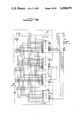
- FIG. 1 is an overall functional block diagram of a specific construction of a preferred embodiment following the teachings of the present invention.
- FIG. 2 is a functional block diagram of the timing section shown as a block in FIG. 1.
- FIG. 3 is a functional block diagram of the foreground generator shown as a block in FIG. 1.
- FIGS. 4A and 4B show a circuit diagram of a specific construction of the object section shown as a logical subsection in FIG. 3.
- FIG. 5 is a circuit diagram of a specific construction of the object control section shown as a logical subsection in FIG. 3.
- FIG. 6 is a circuit diagram of a specific construction of the foreground ROM shown as a logical block in FIG. 3.
- FIG. 7 is a circuit diagram of a specific construction of the object loading section shown as a logical subsection in FIG. 3.
- FIG. 8 is a circuit diagram of a specific construction of the shift register shown as a logical block in FIG. 3.
- FIGS. 9A and 9B are a circuit diagram of a specific construction of the buffer section shown as a logical subsection in FIG. 3.
- FIG. 10 is a circuit diagram of a specific construction of the output section shown as a logical subsection in FIG. 3.
- FIG. 11 is a functional block diagram of the control section shown as a block in FIG. 1.
- FIG. 12 is a circuit diagram of a specific construction of the central section shown as a functional block diagram in FIG. 11.
- FIG. 13 is a functional block diagram of the background generator shown as a block in FIG. 1.
- FIG. 14 is a circuit diagram of a specific construction of the background generator shown as a functional block diagram in FIG. 13.
- FIG. 15 is a circuit diagram of a specific construction of the communication section shown as a logical subsection in FIG. 3.
- FIG. 16 is a detailed functional block diagram of the timing section shown as a simplified schematic in FIG. 2.
- FIGS. 17A and 17B show a circuit diagram of a specific construction of the timing section shown as a functional block diagram in FIG. 16.
- FIG. 18 is a functional block diagram of an overall system combining the elements of FIGS. 1-17.
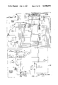
- FIG. 19 is a perspective view of a video game system employing the present invention.
- FIG. 20 is functional block diagram of systems of FIGS. 1 and 18 combined with priority overlay of video foreground objects;
- FIGS. 21 A-B illustrates the spatial correlation of the contents of two object packets in the foreground memory to the respective displayed picture blocks on the display screen
- FIGS. 22 A-B illustrate the different displays resulting from swapping the priority of the object packets in the buffer memory
- FIGS. 23 A-B illustrates the temporal relationship of writing into the buffers in the illustrated embodiments of FIGS. 22 A-B;
- FIG. 24 illustrates the object packet contents as stored in the buffer memory, and illustrates the relationship and mappings of the contents of the buffer to the color ROM, color group latch, and display;
- FIG. 25 is an electronic block diagram illustrating the detailed embodiment as illustrated in FIGS. 26 A-G.
- FIGS. 26 A-G are a specific detailed electronic schematic of the foreground video generator of FIGS. 18-25.
- a specific construction of an embodiment of the present invention is a double line buffer for use with a raster scan color video monitor.
- FIG. 1 shows schematically the logical operation of the specific construction.
- the double line buffer comprises a foreground generator 10 and a background generator 12.
- the foreground generator is block oriented and is also capable of displaying 128 individual, independent objects.
- the background generator is also block oriented and may display selections from 256 different blocks.
- Foreground and background ROM's providing permanent memory means within the respective generators are programmed with information to control the display.
- the foreground and background generators are controlled by a timing section 14.
- the generators output their data into a control section 16.
- a microprocessor 18 governs overall operation of the system.
- the timing section 14 includes a system clock and counters.
- the system clock 30 runs a 10 bit horizontal counter 32, as shown in a simplified schematic, FIG. 2.
- the horizontal counter counts from 0 to 511 during active video scan and from 512 to 634 during horizontal retrace. "Active video scan” is the time during which a horizontal line is actually being traced on the monitor face.
- each horizontal count causes the monitor to draw one horizontal pixel on the screen, except during horizontal blanking, by means that will be described in connection with the "flip" features.
- Each vertical count commences the drawing of one horizontal line by means also to be described in connection with the "flip” feature, except during vertical blanking. Successive horizontal lines are drawn one below another, as the monitor is normally viewed.
- the vertical counter starts at 0 and counts to 239 during active video.
- the video is blanked for retrace for 16 counts commencing with count 239.5, and a second active period starts on a count of 255.5. Blanking again occurs on count 495 for another 16 counts.
- On count 511 the vertical counter is reset to 0 and the cycle recurs.
- the half line count is obtained by detecting the 317th horizontal count.
- the horizontal lines during the second active period, or trace are interlaced between the lines drawn during the first active period.
- the first trace thereby draws a field of the odd numbered lines; the second trace draws a field of the even numbered lines.
- the two interlaced fields or traces together comprise a single "frame" or "picture.”
- the display resolution will be 512 pixels per horizontal line and there will be 479 interlaced lines.
- the foreground generator contains two RAM buffers. Each RAM buffer is capable of holding information for one horizontal, or scan, line. The buffers work as complements of each other. One buffer alternatively unloads its information to the screen on one scan line while the other buffer is loaded with the data for the next scan line. Each scan line is digitized by division into 512 "pixels.”
- the background video display area for the illustrated system is made up of an array comprising blocks 32 pixels wide and 16 lines high. Each block can be individually specified by a programmer to be any one of 256 available pictures.
- a foreground is created by positioning object data in a display buffer at ordered locations having respective associated spatial display locations.
- the foreground data if present, is given priority over the background data present in a background memory in determining the picture to be displayed. If no foreground data is present, such as can be indicated by an all zero, 1, or other code, the background data is instead determinative of the picture to be displayed. In either event, the data determinative of the picture to be displayed is passed to the circuitry for converting said data to signals compatible with driving a raster scan display system.
- the foreground generator 10 is comprised of an object section 20, which provides storage and readout for object packages to be used in the composition of the display.
- a specific construction of the object section is shown in FIG. 4.
- the object packages are stored in an object or foreground RAM 50.
- Each object package comprises four words of information.
- the first word of the package contains a starting vertical position.
- the second word contains a picture number (or index) and an HFLP and a VFLP indicator.
- the third word contains a starting horizontal position.
- the fourth word is a color group which provides a selection of 1 of a plurality of color mappings to be associated and stored with the high priority determinative video data in the buffer.
- the foreground object RAM memory 50 contains the data describing the location on the screen of each of the foreground objects.
- the foreground memory 50 is a read-write memory.
- each object package is comprised of four words of information, comprising a block.
- each block boundary is four-word locations further in memory.
- 32 bits of data are passed for each object packet block.
- Addressing of the next block commences at four address locations subsequent to the starting address for the transfer of the previous object packet block. This is useful, for example, where a counter is loaded with the initial block starting address, and thereafter the counter sequences through the addresses for that block thereby freeing the host processor.
- the ordering of the object packet blocks in the foreground memory 50 is determinative of a priority as among foreground object packet blocks containing identical vertical and horizontal spatial display association.
- the system scans the foreground memory in sequential ascending order, and utilizes horizontal and vertical words from each object packet block to position the associated picture number at the appropriate spatially associated location in the buffer memory. Since, in the illustrated example, the list is scanned in ascending order, the location at which a block is stored in the foreground memory is inversely proportional to the priority of storage in the buffer. As the foreground list is scanned, a subsequent write to the same location overlays the displayable portions of a different object packet block on top of the originally written locations.
- the picture number enables the foreground object memory containing video data corresponding to the picture number to output said data for the line to be displayed to the buffer means for storage at the appropriate location therein.
- the object packet blocks contain video data for a plurality of pixels of display, many of which have no display associated therewith.
- non-display data detection is provided to suppress overwrite of such data to corresponding buffer locations.
- the object RAM 50 comprises four 256 ⁇ 4 Fairchild 93422's addressed in pairs. A read at a single address location thereby causes the RAM to output one byte of data. Four sequential address locations constitute the data for a single object.
- the RAM can store 128 objects at any time.
- the present invention also encompasses other constructions which may have a greater or lesser number of objects, and use more or less than eight bytes of storage per object.
- a 32 bit wide foreground memory 50 is utilized to provide for single-cycle output of entire object packet blocks.
- Other variations can also be utilized in accordance with and complimentary with the present invention.
- an object control section 22 in the foreground generator 10 which provides control for reading object packages out of the object RAM 50.
- An object address counter 52 in the object control section is a nine bit counter which addresses the object RAM locations. This counter is set to zero at the start of every horizontal scan line.
- the object address counter starts at the address of the first object package and counts in steps of 4 in order to determine from the vertical position byte of each package whether an object is to be loaded into one of a pair of RAM buffers 54 and 55 during the current scan line.
- the most significant bit of the nine bit vertical counter may be used as a frame counter to count whether the frame is odd (0 to 239.5) or even (256 to 495).
- the vertical counter will thereby be an eight bit counter for each frame which counts downward starting from zero at the top of the screen.
- the vertical position in each package is specified in the object RAM 50 by counting lines upward starting from zero at the bottom of the screen, as the screen is normally viewed.
- Testing to determine whether an object is to be placed in a buffer may therefore be accomplished by adding the vertical counter contents to the vertical position byte contents from the object RAM 50.
- the four most significant bits become “ones” 16 scan lines before all eight bits become “ones.” This condition occurs once in the even frame and once in the odd frame.
- a test for all "ones" in the four most significant bits therefore permits the object to be placed in one of the buffers 54 or 55 during drawing of 16 horizontal lines before the object's lowest horizontal position line is drawn.
- Addition is performed by an adder 53, in an object section 20 which is fed by the least significant eight bits 57 from the vertical counter and the output 56 of the object RAM 50 which comprises one of the starting vertical position bytes.
- the adder outputs into a vertical latch 58 which is clocked by signals on an LVERT* line and cleared by EOPAC pulses from the object address counter 52.
- the vertical latch 58 in turn outputs the four most significant bits 60 into a load detect circuit 62.
- the load detect circuit which is a NAND gate in the specific construction illustrated in FIG. 4, enables a counter control circuit 65 when the load detect's input is all "ones,” emitting a low logic signal on an LDET* line 64.
- FIG. 6 is a circuit diagram illustrating a specific construction of the foreground ROM 68.
- the four least significant bits 66 from the vertical latch 58 output address terminals A3 through A6 of the foreground ROM 68, and are incremented by one unit at the start of each horizontal line. Terminals A3 through A6 thereby point to successive groups of eight addresses in the foreground ROM. Each group represents data for one horizontal line of a picture.
- the counter control circuit 65 is in object control section 22, and is used to control the frequency and increment size of the object address counter 52. At the start of each horizontal scan the control circuit causes the object address counter to count in 200 nanosecond (ns). steps of 4.
- the load detect circuit 62 determines that an object has to be loaded into the buffer it outputs a low on the LDET* line 64 to the counter control circuit, as already described.
- the counter control circuit 65 switches the count sequence of the object address counter to steps of 1 so that successive bytes of data may be retrieved from the object RAM 50. At the same time the time between steps is increased to 800 nanoseconds to provide time for each object to be loaded into the buffer. As illustrated in FIGS.
- this time can also be different, such as 400 ns.
- the slower counting rate obviates the possibility that the hardware might attempt to load a second object into the buffer before loading of the first one is complete. Once an object has been loaded into the buffer, the counting rate increases to provide for 200 nanosecond steps of 4.
- the second byte out of the object RAM 50 is the picture number of the object being loaded into the buffer.
- the picture number is latched into a picture latch 72 by an LOBJ * signal generated from signals from the object address counter 52 on an OBJ bus 73, as will be described.
- the picture number now comprises the upper address lines 74 to the foreground ROM 68.
- the upper address lines 74 address the block of memory where the representation of the particular picture corresponding to the picture number is stored.
- a byte counter 76 in an object loading section 23, having a specific construction as illustrated in the circuit diagram, FIG. 7, is also enabled by the counter control circuit 65 when the picture number is latched.
- the byte counter addresses the two least significant digits of the foreground ROM, as shown in FIG. 4.
- Count 512 in the object address counter is transmitted as a low on an EOPAC line in the OBJ bus 73, as shown in FIG. 5, to clear the picture latch 72.
- the latch is then enabled at the start of each horizontal scan when the EOPAC line goes high.
- a flip-flop 77 in the object address counter outputs on a START line to reset the object address counter.
- the 634th count from the horizontal counter 32 is transmitted as a low to the flip-flop clear pin 77-1, causing the START line to go low. It will be recalled that the 634th count occurs at the end of horizontal blanking. As the horizontal counter starts counting out the next line, the clear pin 77-1 goes high and flip-flop 77 is enabled. The low on the START line resets the object address counter to zero, as may be seen from FIG. 5.
- the foreground ROM is comprised of four Texas Instruments, Inc. 2732 ROM's.
- the four 4K ⁇ eight-bit ROM's are simultaneously addressed to provide a 4K ⁇ 32 bit memory.
- Another construction of the embodiment may use 2764 ROM's to provide an 8K ⁇ 32 bit, or larger, memory.
- the third byte, the horizontal position byte is output from the object RAM 50.
- the horizontal position and successive bytes are loaded into an eight-bit buffer loading counter 78 during an approximately 3.2 microsec. interval, the time required to scan 32 pixels.
- the counter is clocked at one-half the pixel rate by rises on the line carrying the least significant count from the horizontal counter.
- the byte counter 76 meanwhile counts out bits corresponding to one horizontal line of the picture stored in the foreground ROM 68 causing the ROM to read out the corresponding data.
- the count is from 0 to 3, addressing the two least significant digits of the ROM address. Counting is at the 800 ns. rate; the counter clears on the fourth count.
- ROM picture information for each picture is in the form of a set of words for one frame followed by a set of words for the second frame.
- the data from the ROM 68 is read out in 32 bit words.
- Each word is first loaded into a set of shift registers 80.
- a specific construction of the shift registers is illustrated in FIG. 8.
- the word is shifted bit-by-bit through one of a pair of flip multiplexers 82, 83 and then through one of a pair of data input enable multiplexers 84, 85, which may have a specific construction as indicated in FIGS. 9A and 9B, illustrating a specific construction of a buffer section 23 of the foreground generator 10.
- the flip multiplexers implement a flip feature which will be described.
- the shift registers shift out the bits comprising the word at the same rate that the buffer loading counter 78 is counting.
- the bits are written into one of the buffer RAM's 54, 55 through buffer latches 86, 87. Picture information from the ROM is loaded into successive buffer locations, starting at the location specified by the horizontal position byte.
- the buffer loading counter 78 addresses the buffer RAM's through a 2-to-1 buffer multiplexer 89, shown in FIG. 7.
- the shift registers 80 shift out each word, eight bits at a time.
- the byte counter 76 increments the ROM 68 address and the next 32 bits are loaded into the shift registers. This process occurs a total of four times for one horizontal line of a single object, and a total of 128 bits of data are written into the buffer.
- Each pixel requires four bits of data; 32 pixels thereby comprise a single horizontal line representation of one object.
- color group data is loaded into the successive buffer locations as an attachment to the picture information from the ROM so as to form a picture value comprising a color group subpart common to all pixels within an object packet block and a picture information value as output from the ROM.
- This increases color selection from the color memory.
- This increases the width of the buffer memory storage words to accommodate the increased storage per buffer location for the additional color group information for each location.
- four-bit wide data words must be expanded to eight bits, and four-bit wide 2-to-1 multiplexers must be expanded to eight-bit wide, and so forth.
- the functional aspects of this embodiment are consistent with the teachings herein and hereafter.
- each time data is loaded into one of the buffers 54, 55 data existing in the buffer is first read out and "OR”ed with the incoming data through one of a pair of OR-gates 90, 91; the result of the "OR”ing is then latched into the corresponding buffer latch and read back into the buffer.
- the "OR”ing operation is performed to insure that when picture background information consisting of all zeros is written into the buffer, any object data already existing in the buffer will not be erased.
- zero writes are inhibited by zero detection circuitry.
- Read/writes out of or into the buffers are controlled by a buffer enable 93 which also clocks the buffer latches 86, 87. The time comes to output the data from the buffers at the beginning of each horizontal line.
- the 2-to-1 multiplexer 89 switches the buffer address lines of the selected buffer to couple to the output H0-H8 from the horizontal counter 30. Data coming out of the buffer is latched into one of a pair of data-out latches 94, 95 in an output section 25 of the foreground generator 10. A specific construction of the output section is illustrated in the circuit diagram of FIG. 10.
- the corresponding 512 bytes of data are sequentially read out of the buffer and zeros are written into the corresponding locations by holding all the data-in inputs to the buffer at zero and enabling the write-mode, thereby flushing the buffer.
- the flushing operation is necessary because the buffer has to be cleared of old data (previous horizontal line) before new data (upcoming horizontal line) can be entered.
- a four bit 2-to-1 A-multiplexer 98 switches between the least and most significant four bits at the pixel rate to provide a four-bit wide data stream 99.
- the four bit output of the A-multiplexer makes up one-half of the input to a four bit 2-to-1 B-multiplexer 202 in the control section 16, as may be seen by reference to FIGS. 11 and 12. Background information may make up the other half of the input, as will be described. Whether the background or foreground is selected is determined by the foreground information. If, for example, the foreground data has all zeros in the least significant three bits, as may be deduced from FIG. 12, then the background is displayed, otherwise the foreground is displayed.
- the data from the B-multiplexer 202 indicates an address in a color RAM 204 as illustrated in FIGS. 11 and 12.
- the color RAM is a fast bipolar RAM comprising sixteen 12 bit words. Each 12 bit word can be altered by the programmer and corresponds to a color, thereby providing for 4096 colors, sixteen of which may be displayed at any one time. As the data in the foreground/background combination changes, different locations are addressed in the color RAM and corresponding data outputted to monitor driving circuitry 206.
- the B-multiplexer 202 communicates with the color RAM 204 via a C-multiplexer 208.
- the C-multiplexer is a quadruple 2-to-1 multiplexer which permits the microprocessor to address the color RAM directly.
- the data from the color RAM is converted to voltage levels by a resistor network and a current mirror comprising the monitor driving circuitry and interfaced to the color guns of a color monitor.
- the B-multiplexer 202 communicates with the color RAM 204 through a 2-to-1 C-multiplexer 208.
- the background generator's construction and operation may be understood by reference to FIGS. 13 and 14.
- the background display comprises an array of 32 blocks width by 30 blocks high. Each block is 16 pixels wide and sixteen lines high.
- the background display may control the pixels in pairs, thereby decreasing the resolution of the background as compared with the foreground.
- the display information for each pair of pixels then comprises two bits of data.
- a 1K ⁇ 8 background RAM 302 may be used to store a set of data bytes which serve as pointers to the 32 ⁇ 30 array.
- Each eight-bit byte of data in the RAM 302 points to an initial address in the 4K ⁇ 8 background ROM 304.
- the particular background ROM then contains 256 different pictures which may be selected for display in each block of the array.
- the background RAM 302 is addressed by a 2-to-1 background multiplexer 306.
- the background multiplexer under control of the microprocessor, selects either the microprocessor address bus 308 or a ten-bit timing bus 210 from the timing selection.
- the most significant bits on the timing bus are the fourth through seventh most significant bits of the vertical count, V3-V7; the remaining bits are the five most significant horizontal count bits, H4-H8, as shown in FIG. 13.
- the lower order horizontal and vertical counter bits are not used for addressing the background RAM thereby insuring that the address lines to the RAM change only 32 times during a horizontal line and 32 times for a vertical scan. That is, the address lines change only on every 17th horizontal count and every 9th vertical count.
- the same eight bits of data appear at the output of the background RAM 302.
- the background RAM 302 output is latched into a background latch 312.
- the latched data becomes the upper address lines to the background ROM 304.
- Latching is clocked by NAND gate 313 on the third horizontal count after the RAM address changes in order to accommodate the access time of the RAM.
- the three least significant vertical count bits and the fourth least significant horizontal count bit make up the low order address lines to the background ROM 304, also as shown in FIG. 14.
- the upper address lines thereby remain fixed while the low order lines count out bytes in the background ROM on every ninth horizontal count during the scan of a single line.
- the eight bits of data comprising one byte from the background ROM are then latched into a background out latch 314.
- the eight bits comprise data representing four pars of pixels.
- a 4-to-1 multiplexer 316 converts the eight bits into a two bit wide stream 318.
- the multiplexing is controlled by the second and third least significant horizontal counter bits, thereby providing a background resolution one-half that of the foreground.
- the 2-bit wide stream 318 from the 4-to-1 multiplexer inputs to the alternate least significant input bits of the 2-to-1 B-multiplexer 202, as indicated in FIGS. 11 and 12.
- the output of the B-multiplexer addresses the color RAM through the 2-to-1 C-multiplexer 206, as already described.
- An alternative construction of the embodiment may use separate color RAM's for foreground and background.
- the second set of inputs of the C-multiplexer may be connected to the microprocessor, thereby providing a capability of direct microprocessor control of the color output from time to time.
- the background RAM is partially updated from time to time during vertical blanking. Update is dictated by the play of the game. In normal play, only a very few background blocks will need to be altered and even a very slow microprocessor will have time to make the alterations during vertical blanking.
- Data for the background RAM is taken off the microprocessor data bus by a bi-directional buffer 220 as described earlier with reference to the foreground data.
- a staging RAM 402 in a communications section 26 may be utilized for communication with the controlling CPU (which may be microprocessor based) as shown in FIG. 3.
- FIG. 15 is a circuit diagram of a specific construction of the communication section. Data is moved from the staging RAM to the object RAM 50 during every second vertical blanking time at intervals of approximately 1/30 sec. The total move takes eight horizontal line times--approximately 508 microseconds in the specific construction described herein. During the move time a staging multiplexer 404 addressing the staging RAM selects a transfer counter 405 as input. An object multiplexer 406 addressing the object RAM simultaneously selects the transfer counter as input. Selection occurs at the beginning of the final eight vertical counts of the second vertical blank period. In the specific construction shown in FIG. 11 there is provision for the microprocessor to prevent the selection from occurring.
- the transfer counter 405 steps through successive locations in the staging RAM 402; the data from the staging RAM is presented as input to the object RAM 50.
- a write enable signal is also generated by the transfer counter from the clock 30 and horizontal counter 32 and sent to the object RAM for each address. Because the address lines to each of the RAM's are identical, data is therefore transferred from the staging RAM 402 to the object RAM 50.
- An interrupt signal sent to the microprocessor by the transfer counter 405 at the beginning of the transfer is used to inhibit the microprocessor from transferring data during the next 508 microseconds, during the time the staging RAM 402 is transferring its data.
- the data transfer occurs between vertical counts 496 and 503.
- the staging multiplexer 404 switches and allows the microprocessor address bus to address the staging RAM.
- the object multiplexer 406 at the same time, allows the object address counter 52 to address the object RAM for readout purposes.
- the staging RAM is thereby available to be refreshed by the microprocessor except during vertical counts 496 to 503.
- Microprocessor data is input into the staging RAM through a bi-directional buffer 410 which may communicate with a microprocessor data bus 412.
- the transfer counter 405 operates upon combinations of outputs from the horizontal and vertical counters. In the specific construction it is a nine bit counter. The five least significant bits are the five most significant horizontal count bits, as shown in FIG. 15. The three most significant bits are the three least significant vertical count bits. The counter thereby counts from zero to 1023 during the time required to draw four horizontal lines. Thus, in the specific construction, only one-half the available time is used for data transfer.
- the staging RAM in FIG. 15 is constructed utilizing a pair of commercially available Intersil IM2114 RAM's with 1024 ⁇ 4-bit memories.
- the flip feature is associated with the timing and foreground sections and controlled, in the specific construction, by the microprocessor.
- the underlying principle of the flip feature involves complementary, or backward, counting as a method for inverting and/or obtaining right-to-left reversal of the images presented on the screen.
- the embodiment described herein readily lends itself to complementary counting which, properly applied, merely reverses the horizontal and/or vertical scanning directions of the raster scan.
- a FLIP command from the microprocessor inverts the entire picture, interchanging right-left and up-down, as required for a cocktail table game where two players are sitting opposite each other.
- the FLIP command affects the output of the timing section.
- FIG. 16 is a more detailed schematic of the timing section than the simplified schematic in FIG. 2.
- the horizontal counter 32 of FIG. 2 is seen to comprise a horizontal first counter 500 and a FLIP horizontal logic circuit 502.
- the horizontal first counter 500 comprises a plurality of horizontal synchronous counters 510 feeding a horizontal logic circuit 512 as may be seen in the circuit diagram, FIG. 17.
- the horizontal counters are clocked by the leading edges of the positive 100 microsec.
- HCLK pulses from the system clock 30.
- the horizontal logic circuit emits a low on the 317* line on the 317th count, and a low on a 634* line on the 634th count.
- the 634* low is fed back to, and resets the horizontal synchronous counters 510, causing it to output lows on each of ten output lines, SH0 to SH9.
- the horizontal synchronous counters are thereby reset on every 635th count.
- the horizontal synchronous counters 510 are clocked by the 100 ns.
- HCLK pulses generated by the system clock 30 and the D-type flip-flop 514.
- the HCLK pulses cause the counters to count on the output lines SH0-SH9 which are numbered in increasing order of significance.
- the vertical counter 34 of FIG. 2 is seen to comprise a vertical first counter 520 and flip vertical logic 522, as shown in FIG. 17.
- the vertical first counter comprises a plurality of vertical synchronous counters 530 and a vertical logic circuit 532.
- the vertical logic circuit 532 emits a high (low) on the VBLK (VBLK*) line between vertical counts 239.5 and 255.5 and between vertical counts 495 and 511, as previously described.
- the vertical logic circuit also emits a low on a 511* line on count 511.
- the vertical synchronous counters 530 are clocked by the SH9 line from the horizontal synchronous counters 510.
- the SH9 line goes high, as described, on every 635th count.
- the SH9 line is also the HBLK line to the monitor.
- the vertical synchronous counters are consequently advanced at the beginning of each HBLK period.
- the vertical synchronous counters 530 are reset every 512th count by a low on the 511* line.
- the 511* low is a short pulse because the counters are reset substantially as soon as the 511* line goes low.
- Circuit diagrams for the FLIP horizontal and vertical logic 502, 522 are also displayed in FIGS. 17A and 17B.
- the SH0 to SH5 outputs of the first horizontal counter 500 are fed to the input of a 74S174 D-type flip-flop 540 having a short set-up time approximately 5 ns.
- the outputs corresponding to inputs SH0 to SH2 are each fed to one of a first plurality of exclusive OR-gates 542.
- the second input to each of the exclusive OR-gates 542 is a FLIP line from the microprocessor.
- each of the exclusive OR-gates 542 is fed to a different one of a triad of exclusive OR-gates 544, each also having the FLIP line as input.
- the outputs of the OR-gates 544 corresponding, respectively, to the inputs SH0 to SH2 are labeled*H0 to *H2.
- the flip-flop 540 is triggered by an SQ2C* signal from the load detect circuit which is shown in FIG. 4.
- the SQ2C* signal because of delays in a pair of inverters 546, 548 OR-gates 550, 552, and flip-flop 554, all shown in FIG. 6, resembles an HCLK signal delayed by about 15 ns.
- the *H0-*H2 signals in consequence, taking into account delays in the exclusive OR-gates 542, 544 are delayed about 50 ns. with respect to the SH0-SH2 signals.
- the *H0-*H2 signals are substantially unaffected by the state of the FLIP line. If FLIP is low, each exclusive OR-gate transmits the signals from SH0-SH2 unaffected. If FLIP is high then each exclusive OR-gate complements the signals and the resulting double complement leaves the signal unaffected.
- Signals SH3-SH9 are clocked through the flip-flop 540 and then each is fed to a different exclusive OR-gate of the triad 556.
- the exclusive OR-gates output signals, respectively, H3-H9 which are delayed by about 25 ns. with respect to SH3-SH9.
- the FLIP line is a second input to each of the plurality of gates 556.
- the signals *H0-*H2 are fed to a triad of inverters 564 to generate the complementary signals H0* -H2*.
- the flip vertical logic 522 comprises an octal D-type flip-flop 566 and a set of nine exclusive OR-gates 568.
- the FLIP line is an input to each exclusive OR-gate.
- the vertical first counter 520 output V0-V7 is input to the flip-flop 566.
- the eight output lines from flip-flop 566 are each fed to a different one of the exclusive OR-gates 568, V4-V7 also feeding through adder 569.
- the V8 output from counter 520 is fed directly to the remaining one of the exclusive OR-gates 568.
- a set of output signals DV0-DV8 are thereby respectively generated through the flip-flop 566 and exclusive OR-gates 568 as shown explicitly in FIG. 17.
- a flip-flop 566 is clocked by the START line from the object address counter 52.
- the START line it will be recalled, goes low just before the start of each horizontal line. It goes high on the first count from the counter control circuit which will be at the count of either the first or fourth horizontal pixel, depending upon whether an object is to be loaded.
- START goes high the current vertical count V0-V7, is clocked into flip-flop 566 and through eight of the exclusive OR-gates 568, to generate the output signals DV0-DV7.
- the even or odd frame count bit, V8 is fed directly to the ninth of the exclusive OR-gates 568.
- the DV0 output also inputs to an inverter 570 to generate a complementary output DV0*.
- the adder 569 adds 16 to the complimented vertical count to compensate for the displacement introduced by VBLNK when counting backward from 511.
- activation of FLIP by the microprocessor causes the significant horizontal and vertical counter bits to be complemented and will thereby cause the line buffer system to invert up-down and right-left in presenting its display
- An HFLP and a VFLP feature of the embodiment provide for inversion of a single object.
- the VFLP and HFLP indicators are, respectively, the most significant bit and next most significant bit in the second byte of each object package.
- the HFLP and VFLP indicators are loaded into the picture latch 406 when an object is to be displayed. When either indicator is high the corresponding feature is enabled, as may be seen explicitly in FIG. 4.
- the VFLP line provides one input to each of five exclusive OR-gates 574.
- the other input to each OR-gate is one of the lines carrying the four least significant bits from the vertical latch 58.
- the remaining one of the exclusive OR-gates 574 carries the even-odd frame count bit DV8.
- the outputs from the exclusive OR-gates 574 address terminals A2 to A6 of the foreground ROM as already described
- the HFLP line acts in an analogous fashion to the VFLP line.
- the HFLP line When the HFLP line is high it causes the pair of exclusive OR-gates 576 to complement the input to the two least significant address pins of foreground ROM 68.
- the four words comprising a line of a picture are thereby read out in backward order.
- the HFLP high also selects the B-inputs from flip-muxes I and II, 82, 83 . . . .
- the B-inputs contain the output from shift registers 80 in inverted order from the A-outputs. As a result, the picture information will ultimately be read out backward, corresponding to right-left inversion, or reflection, of an individual picture.
- FIG. 18 is a block diagram illustrating the functional blocks of a complete video display system as taught in FIGS. 1-17.
- a player stimulus signal is output from input means 660 responsive to player activation of a player control, such as joystick 695 or pushbutton 691-693 of FIG. 19.
- a control means 605 provides appropriate address, data and control signals to selectively store foreground and background object packet lists for storage in the foreground means 610 and background means 620, respectively.
- the foreground means 610 can be the system as illustrated in FIG. 3.
- the background means 620 can be the system as illustrated in FIG. 13.
- the video data corresponding to foreground and background object selection data are coupled from the foreground means 610 and background means 620 to the foreground/background selector means 630 which selectively provides output of either the foreground or background video data.
- the selection of the foreground/background selector means 630 is determined responsive to the presence or absence of foreground video display data. If no video display data is present for a particular foreground location, then the selector means 630 selects the background object video display data for display.
- the output from the foreground/background selector means 630 is a video data signal which is coupled to the color memory 640 which selects one of a plurality of colors for association with a respective location on the display 670 corresponding to the video data from the selector means 630.
- the output from the color memory 640 is a multi-bit color value signal which is coupled to digital to analog converter 650 which converts the digital color value signals output from the color memory 640 to analog picture signals for driving the display 670.
- One embodiment of the foreground/background selector means 630, color RAM 640, digital analog conversion means 650, and associated display driver circuitry are illustrated in FIG. 10.
- the selector means 630 is represented by the blocks 25, 202, and 209.
- the color memory is represented at block 204.
- the digital to analog conversion circuitry is illustrated at block 206.
- the video game system in block 700 is comprised of a cabinet housing 698 containing all necessary electronics therein.
- a display screen 697 is provided for player viewing.
- the display 697 is provided on a slight vertical incline for viewing comfort by the player.
- the display 697 is a raster scan display.
- the housing 698 also includes user input means for providing a source of player-provided stimuli for transfer to the system electronics.
- the player input control means include a joystick 695, and pushbuttons 691, 692 and 693.
- the joystick 695 provides signals responsive to user movement of the joystick in a 360° radius about the center pivot point of the joystick to control interraction of the player with the game play and logic.
- the pushbuttons 691 and 692 provide for 1 and 2 player selection of the game.
- the pushbutton 693 can be used to start the game, or may alternatively be utilized during the play of the game for various purposes.
- a coin slot mechanism 694 is provided on the front of the cabinet 698 to accept user coins or tokens to activate credits for game plays.
- Each game play can comprise multiple turns per single player, or can comprise alternating multiple turns for multiple players. Additionally, fewer or lesser numbers of joysticks and pushbuttons can be provided according to the requirements of the video game desired.
- an input means 702 provides an output signal responsive to an external player-provided stimulus, such as a signal output responsive to player movement of the joystick 695 or one of pushbuttons 691-693 of FIG. 19.
- a control processor system 705 provides control of display presentation to be made upon the display 770 responsive to stored and predefined game logic and the output signal from the input means.
- the display means 770 provides a raster scan video display comprising a plurality of display lines. Each display line is further comprised of a plurality of display segments.
- the video display is provided responsive to picture signals as output from the display source selector 740, as discussed further hereinafter.
- the processor 705 causes object information to be selectively output from foreground object storage means 720 from predefined locations therein, in the form of blocks of foreground data, each such block corresponding to a display segment of the video display.
- the processor 705 also controls the selective outputting of background information from the background memory 715 in the form of blocks of background data, each such block corresponding to a display segment of the video display.
- a buffer 730 provides means for selectively storing foreground data corresponding to a plurality of adjacent display lines on the monitor screen during active video display of a picture containing one of the adjacent display lines.
- Selection means comprising the processor system 705 and overlay control circuitry 725, control the priority of display of overlaid objects for each single location on the display.
- the selection means controls the selective overwriting of object information representing multiple object data packets representing multiple pictures to single buffer locations, selectively overlaying only display video data, with the result as shown in FIGS. 21-23.
- the selection means selectively stores object information representing at least two different objects at the same location in the buffer, overwriting the object information first stored at the location in the buffer with a display part of the object information stored second in the location in the buffer.
- the display part of the object information refers to display data. Any default signal pattern indicating non-display data can be detected and utilized to inhibit overwriting of data to corresponding locations, such as zero detection.
- the controller 740 selectively provides picture signals to the display 770 for providing a picture display thereupon responsive to the foreground and the background video data as output from the buffer 730 and background memory 715, respectively.
- the lack of displayable foreground video data enables the selection and display of the corresponding background video data for the respective display location.
- the selection means provides for selective overwriting of object information representing multiple object data packets.
- the order in which the object data is written into the buffer is determinative of the overlay pattern which will result on the video display 770.
- the processor 705 provides means for writing a list of object information in a selectable order into a foreground read-write memory 710. The order of prioritization of said object information can be determined by the order in which the object information is located within the foreground memory 710. If the foreground memory 710 is then scanned in a sequential ascending order, the higher addresses will then represent higher priority objects to be overlaid onto lower priority objects corresponding to the same buffer and display locations.
- the output from the foreground memory 710 is coupled to and drives the foreground object memory 720 for providing blocks of corresponding foreground data for coupling to the buffer 730 and overlay control circuit 725 to provide for writing to locations in the buffer 730 responsive to the blocks of foreground data as stored in the foreground memory 710.
- the priority of overlay of object information can thus be determined responsive to the order in which the object information is output from the foreground memory list means 710.
- the overlay control circuit 725 is coupled to the output from the foreground object memory 720 and provides an output to the buffer 730.
- the overlay control circuit 725 inhibits writing of object information to locations containing display data when the object information to be overwritten consists of non-display data. This is illustrated in greater detail in FIGS. 25 and 26.
- the buffer 730 of FIG. 20 is comprised of a pair of random access memories 1270 and 1280 which are alternately refreshed and displayed. During active video display of a display line corresponding to the output of the contents of one of the pair of random access memories the other of the pair being refreshed (i.e. loaded).
- a shift register 1230 couples object packet information from the foreground object storage memory 1220 (e.g. 720 in FIG. 20), to the buffer memories 1270 and 1280 (730 of FIG. 20).
- FIGS. 21 A-B the spatial correlation of the contents of two object packets in the foreground memory 720 to the respective corresponding displayed picture blocks on the display 770 are illustrated.
- the two object data packets, object 1 data packet 810, and object 3 data packet 820, of Fig. 21 A correspond to the two display picture blocks 811 and 821 of FIG. 21 B, respectively.
- the picture block for object packet 1 comprises a brick wall having an opening in the center thereof corresponding to non-display data.
- the picture block 821, corresponding to object packet 3 illustrates a man standing up, with a background of non-display data.
- FIGS. 22 A-B one of the benefits achieved utilizing the present invention is illustrated by swapping the order of writing of the object packet 1 and 3 into the buffer memory.
- the order of writing of the object packets to the buffer memory determines the priority of overlay in the illustrated embodiment. This can be more clearly seen by referring to FIGS. 22 A-B and 23 A-B together.
- FIGS. 23 A-B illustrate the temporal relationship of writing into a single location in the buffers, relative to the priority ordering relationship of the overlaid display respectively illustrated in FIGS. 22 A-B.
- the object packet 1 is first written to the buffer memory, followed by the writing of object packet 3 at some later time, as shown in FIG. 23 A.
- the resultant display picture block is illustrated in FIG. 22 A, showing the man with the brick wall having an opening therein positioned behind him.
- picture block 811 has been selectively and partially overlaid with picture block 821 only insofar as the picture block 821 contains displayable video data.
- FIGS. 22 B and 23 B By reversing the priority of writing, the opposite effect is achieved, as shown in FIGS. 22 B and 23 B.
- FIG. 22 B by first writing the object packet 3 data into the buffer at a selected address, and then, for the same display line, writing object packet 1 to the same location, at a later time, a reversed priority display is obtained as shown in FIG. 22 B.
- FIG. 22 B a portion of the man is seen through the opening in the wall.
- the picture block 821 is overlaid with the picture block 811, only as to displayable video data. Since the opening in the wall does not consist of displayable video data, the portion of the video data corresponding to object packet 3 representing the man is preserved in the display in the opening of the brick wall.
- 22 B is accomplished by simply reversing the order in which the object data packets are written to a single location in the buffer memory. This concept can be expanded to multiple selective overlays of a plurality of different object packets to a single location. Alternatively, the order of addressing the foreground memory 710 can be varied to vary the order of writing to the buffer 730. Other selectively variable priority ordering techniques can also be utilized.
- color memory 710 the relationship and mappings of the contents of the color memory 710, color object memory 720, color group latch 950, and buffer memory 730 is illustrated.
- the object packet in the illustrated embodiment is comprised of four words of information.
- foreground memory 710 contains four-word object packets, such as packets 920 and 930.
- each packet is comprised of four words comprising a starting vertical position word Vpos, 921, a picture number word, PICT, 922, a color group word, C.G., 923, and a horizontal position word, Hpos, 924.
- the foreground object memory 720 provides corresponding pixel object packets, such as object packet 910, responsive and corresponding to the picture number as output from the foreground memory 710.
- the pixel object packet 910 is comprised of 32 pixels corresponding to a foreground display pixel block.
- the foreground object memory 720 is also responsive to video timing signals for determining the proper pixels within the object packet 910 for output to the buffer 730.
- the color group information, e.g. 923, corresponding to the picture number, e.g. 922, as output to the foreground object memory 720, is stored in a color group latch 950.
- the color group word as stored in the latch 950 is output from the color latch 950 so as to be combined with the pixel data output from the foreground object memory 720 prior to storage in the buffer 730.
- the buffer 730 provides for combined storage of each pixel and the associated color group word in associated locations in the buffer 730, as shown in FIG. 24.
- object packet 910 in the illustrated embodiment, corresponds to the buffer packet 911 which combines the color group word as output from the color group latch 950 with the associated pixel data.
- the determination of when and where to place the combined pixel and color group data into the buffer is made responsive to the vertical position data Vpos from the foreground memory object respectively associated with the combined data being stored in the buffer.
- the video timing and horizontal position data Hpos from the respectively associated foreground memory object packet respectively in combination with the vertical position data Vpos are determinative of the selected locations within the buffer 730 where the combined data will be stored.
- the combined data is output, a pixel and color group word for each color value, to a display driver 740 which provides video picture signals to drive the display 770.
- FIG. 25 a detailed electronic block diagram of a foreground generator system having priority overlay of foreground object packets is shown, corresponding to the detailed electrical schematic of FIGS. 26 A-G.
- the detailed electronic circuitry of FIGS. 26 A-G are blocked in functional subgroupings and numbered corresponding to the respectively numbered functional blocks of FIG. 25.
- the discussion hereafter relative to FIG. 25 applies to the FIGS. 26 A-G which corresponds to a detailed embodiment of the elements of FIG. 25.
- FIGS. 25 and 26 A-G correspond to an enhanced version of the systems as illustrated in FIGS. 3 and the detailed electrical drawings thereof (e.g. FIGS. 4-10, and 15).
- FIG. 25 and 26 A-G correspond to an enhanced version of the systems as illustrated in FIGS. 3 and the detailed electrical drawings thereof (e.g. FIGS. 4-10, and 15).
- the microprocessor such as the microprocessor system 705 of FIG. 20, provides data address and control signals to a bi-directional buffer 1110, a 2-1 mux 1100, and a 2-1 mux pair 1100 and 1140, respectively.
- An object address counter is initialized responsive to control signals, and passes an object address value to an object latch 1150 which provides an output to the other input of the 2-1 multiplexer 1140.
- a staging RAM 1120 selectively stores data from the microprocessor responsive to the 2-1 multiplexer 1100 and the bi-directional buffer 1110, so as to store the equivalent list of foreground object data in a manner so as not to interrupt the normal processing cycles of the system.
- the output of the staging RAM is coupled to the data input of the foreground object memory 1130, which is also coupled to the output of the bi-directional buffer 1110.
- This allows either direct loading of data from the microprocessor, or passing of data from the staging RAM to the object RAM in a manner independent of and asynchronous to transfer of data from the microprocessor to the staging RAM.
- the staging RAM acts to provide a buffer to isolate loading of object list data, and provide for minimal interruption in processing the power due to overhead in loading the foreground data list.
- the miscellaneous control circuitry 1360 provides for decode of video timing data and performs various other miscellaneous control functions.
- the circuitry of 1370 provides additional horizontal timing control signals.
- the data from the staging RAM is transferred to the object RAM in a manner to avoid interference with operation of the processor system and the operation of the foreground system, as discussed with reference to FIGS. 3 et seq. in the operation of the staging system.
- the four words in the object packet within the foreground memory 1130 includes Vpos, picture number data, color group data, and Hpos data.
- each of the four words is output and coupled to respective circuitry for performing the functions as described above herein with reference to FIG. 24.
- the Vpos data is coupled to the input of adder 1170, to be processed along with an input from the raster scan video timing circuitry Vdpos.
- the output of the adder 1170 is coupled to the vertical latch 1180 which provides outputs to a load-detect circuit 1190 and to the foreground object memory 1220.
- the load-detect circuitry 1190 provides an output to the counter control circuitry.
- the picture number data output from the foreground memory 1130 is coupled to the picture number latch 1200 which provides an output to the foreground object memory 1220.
- Video timing circuitry provides a load object signal to clear a byte counter 1210 which is then clocked to provide an output coupled to the input of the foreground object memory 1220.
- the foreground object memory 1220 provides the object picture memory data packet output responsive to the output from the vertical latch 1180, the picture number latch 1200, and the byte counter 1210.
- the foreground object memory provides four words of output in parallel, as illustrated in detail in FIGS. 26 F-G.
- the shift registers 1230 perform word-size conversion in conjunction with the buffer input multiplexers 1290 and 1300 for compatability with the word-size and timing of the buffers 1270 and 1280.
- the Hpos data is coupled to the input of the buffer loading counter 1240 which provides outputs to multiplexer circuitry 1260.
- the multiplexer 1260 is responsive to the buffer loading counter 1240 and horizontal timing from the video timing circuitry to provide an output.
- the output from the multiplexer 1260 enables the addressing of locations in the buffer memories 1270 and 1280 having a spatial correlation to the respective object packets Hpos data.
- the color group word is coupled from the foreground memory 1130 to the input of the color group latch 1250.
- the output from the color group latch 1250 is coupled to the buffers 1270 and 1280, in a selective manner, so as to be stored and associated with respective pixel data values as output from the foreground object memory 1220 responsive to the picture number corresponding to the color group number for the object packet from the foreground memory 1130.
- the outputs from the line buffers 1270 and 1280 are coupled to output control latches 1310 and 1320, respectively, which in an alternating manner display the contents associated with one of the buffers 1270 and 1280 while the other of the buffers 1270 and 1280 is being loaded with display data for a subsequent display line.
- the output of the control latches 1310 and 1320 are coupled to a 2-1 multiplexer 1330 to provide word size conversion for providing an output of video data vid 0-vid X, including color group data and associated pixel data, for coupling to the foreground/background selector means, such as controller 740 of FIG. 20.
- the starting address is loaded into the counters 1240 at the same time that the color group word is loaded into the color group latch 1250.
- the circuitry 1260 provides for selection of one of the buffers 1270 or 1280 responsive to timing and gating signals.
- the 2-1 address multiplexer 1100, foreground staging memory 1120, bi-directional buffer 1110, and miscellaneous control circuitry 1360 are shown in detail in FIG. 26 A. Additional details of the miscellaneous control circuitry 1360 are shown in FIG. 26 B, which also illustrates the details of the object address counter 1160.
- the foreground object memory 1130 portions of the miscellaneous control circuitry 1360, adder circuitry 1170, vertical latch circuitry 1180, load-detect circuitry 1190, and buffer loading counter 1240 are shown in detail in FIG. 26 C.
- a second part of the vertical latch 1180, the byte counter 1210, the 2-1 multiplexer circuitry 1260, write-control circuitry 1350 associated with the suppression of non-video data in conjunction with the zero detect circuitry (i.e. 1340 of FIG. 26 E), and the double-line buffer RAM 1270 and 1280 are shown in detail in FIG. 26 D.
- the picture number latch 1200, the zero detection circuitry 1340 i.e.
- FIG. 26 E details are illustrated for the foreground object memory 1220 (e.g., illustrated as read-only memory circuits), buffer input multiplexers 1290 and 1300, object packet shift registers 1230, and additional horizontal timing circuitry 1370.
- the additional horizontal timing circuitry 1370 provides the horizontal clock bar HCLK signal output utilized in the write-control circuitry 1350 in conjunction with the zero detection outputs and the nd.0. to nd3 outputs from zero detection circuitry 1340 to control the selective overwriting of display video data, inhibiting the overwriting of non-display video data.
- FIG. 26 G illustrates a detailed embodiment of the foreground object memory 1220 (e.g. illustrated as ROMs) and shift registers 1240.
Abstract
Description
Claims (33)
Priority Applications (1)
| Application Number | Priority Date | Filing Date | Title |
|---|---|---|---|
| US06/520,762 US4498079A (en) | 1981-08-20 | 1983-08-08 | Prioritized overlay of foreground objects line buffer system for a video display system |
Applications Claiming Priority (2)
| Application Number | Priority Date | Filing Date | Title |
|---|---|---|---|
| US06/294,438 US4398189A (en) | 1981-08-20 | 1981-08-20 | Line buffer system for displaying multiple images in a video game |
| US06/520,762 US4498079A (en) | 1981-08-20 | 1983-08-08 | Prioritized overlay of foreground objects line buffer system for a video display system |
Related Parent Applications (1)
| Application Number | Title | Priority Date | Filing Date |
|---|---|---|---|
| US06/294,438 Continuation-In-Part US4398189A (en) | 1981-08-20 | 1981-08-20 | Line buffer system for displaying multiple images in a video game |
Publications (1)
| Publication Number | Publication Date |
|---|---|
| US4498079A true US4498079A (en) | 1985-02-05 |
Family
ID=26968528
Family Applications (1)
| Application Number | Title | Priority Date | Filing Date |
|---|---|---|---|
| US06/520,762 Expired - Lifetime US4498079A (en) | 1981-08-20 | 1983-08-08 | Prioritized overlay of foreground objects line buffer system for a video display system |
Country Status (1)
| Country | Link |
|---|---|
| US (1) | US4498079A (en) |
Cited By (35)
| Publication number | Priority date | Publication date | Assignee | Title |
|---|---|---|---|---|
| US4599610A (en) * | 1984-03-21 | 1986-07-08 | Phillips Petroleum Company | Overlaying information on a video display |
| US4616336A (en) * | 1983-05-11 | 1986-10-07 | International Business Machines Corp. | Independent image and annotation overlay with highlighting of overlay conflicts |
| US4675666A (en) * | 1983-11-15 | 1987-06-23 | Motorola Inc. | System and method for altering an aspect of one of a plurality of coincident visual objects in a video display generator |
| US4688181A (en) * | 1982-12-22 | 1987-08-18 | International Business Machines Corporation | Image transformations on an interactive raster scan or matrix display |
| US4744047A (en) * | 1984-11-01 | 1988-05-10 | Hitachi, Ltd. | Pattern test apparatus including a plurality of pattern generators |
| US4754966A (en) * | 1983-10-19 | 1988-07-05 | U.S. Philips Corp. | Circuit for forming objects in a video picture |
| US4774506A (en) * | 1984-10-05 | 1988-09-27 | Thomson-Csf | Process for producing synthetic video images for real time visual display and high information density and apparatus using this process |
| US4878181A (en) * | 1986-11-17 | 1989-10-31 | Signetics Corporation | Video display controller for expanding monochrome data to programmable foreground and background color image data |
| US4951229A (en) * | 1988-07-22 | 1990-08-21 | International Business Machines Corporation | Apparatus and method for managing multiple images in a graphic display system |
| US5016876A (en) * | 1988-10-14 | 1991-05-21 | Williams Electronics Games, Inc. | Video display co-processor for use in a video game |
| US5254984A (en) * | 1992-01-03 | 1993-10-19 | Tandy Corporation | VGA controller for displaying images having selective components from multiple image planes |
| US5271097A (en) * | 1988-06-30 | 1993-12-14 | International Business Machines Corporation | Method and system for controlling the presentation of nested overlays utilizing image area mixing attributes |
| WO1996020470A1 (en) * | 1994-12-23 | 1996-07-04 | Philips Electronics N.V. | Single frame buffer image processing system |
| US5621431A (en) * | 1994-04-29 | 1997-04-15 | Atari Games Corporation | Animation system having variable video display rate |
| US5632681A (en) * | 1995-03-07 | 1997-05-27 | International Business Machines Corporation | Universal electronic video game renting/distributing system |
| US5638094A (en) * | 1994-11-01 | 1997-06-10 | United Microelectronics Corp. | Method and apparatus for displaying motion video images |
| US5707288A (en) * | 1994-12-31 | 1998-01-13 | Sega Enterprises, Ltd. | Video game system and methods for enhanced processing and display of graphical character elements |
| US5742271A (en) * | 1993-11-11 | 1998-04-21 | Seiko Epson Corporaiton | Matrix type display device, electronic system including the same and method of driving such a display device |
| US5748174A (en) * | 1994-03-01 | 1998-05-05 | Vtech Electronics, Ltd. | Video display system including graphic layers with sizable, positionable windows and programmable priority |
| US5941775A (en) * | 1994-10-14 | 1999-08-24 | Sega Of America, Inc. | Data processing system, method thereof and memory cassette |
| US5982350A (en) * | 1991-10-07 | 1999-11-09 | Eastman Kodak Company | Compositer interface for arranging the components of special effects for a motion picture production |
| US6010405A (en) * | 1994-12-30 | 2000-01-04 | Sega Enterprises, Ltd. | Videogame system for creating simulated comic book game |
| US6113494A (en) * | 1997-06-17 | 2000-09-05 | Intel Corporation | Using multiple prioritized statements of abstracted intention to align different views |
| US6224485B1 (en) | 1998-05-01 | 2001-05-01 | Midway Amusement Games, Llc | High-score display system for a video game |
| US6269403B1 (en) | 1997-06-30 | 2001-07-31 | Microsoft Corporation | Browser and publisher for multimedia object storage, retrieval and transfer |
| US20020193161A1 (en) * | 2000-01-25 | 2002-12-19 | Katsuhiro Ishii | Game system, program and image generation method |
| US20020196461A1 (en) * | 2001-06-25 | 2002-12-26 | Hanna Stephen D. | Compressed data transmission over a plurality of transmission paths |
| US20030093331A1 (en) * | 2001-11-13 | 2003-05-15 | International Business Machines Corporation | Internet strategic brand weighting factor |
| US6604144B1 (en) * | 1997-06-30 | 2003-08-05 | Microsoft Corporation | Data format for multimedia object storage, retrieval and transfer |
| US20040199419A1 (en) * | 2001-11-13 | 2004-10-07 | International Business Machines Corporation | Promoting strategic documents by bias ranking of search results on a web browser |
| US6924821B2 (en) * | 2000-04-01 | 2005-08-02 | Autodesk Canada Inc. | Processing pipeline responsive to input and output frame rates |
| US7289823B1 (en) | 2004-06-28 | 2007-10-30 | Neomagic Corp. | Video overlay buffer mirrored through a shared mailbox between two processors in a feature phone |
| US7307635B1 (en) | 2005-02-02 | 2007-12-11 | Neomagic Corp. | Display rotation using a small line buffer and optimized memory access |
| US20080163060A1 (en) * | 2007-01-03 | 2008-07-03 | Microsoft Corporation | Motion desktop |
| US20100117996A1 (en) * | 2005-12-02 | 2010-05-13 | Kim Sang-Hun | Display device capable of performing left/right change display and display method thereof |
Citations (7)
| Publication number | Priority date | Publication date | Assignee | Title |
|---|---|---|---|---|
| US4070710A (en) * | 1976-01-19 | 1978-01-24 | Nugraphics, Inc. | Raster scan display apparatus for dynamically viewing image elements stored in a random access memory array |
| US4112422A (en) * | 1976-12-13 | 1978-09-05 | Atari, Inc. | Method and apparatus for generating moving objects on a video display screen |
| US4116444A (en) * | 1976-07-16 | 1978-09-26 | Atari, Inc. | Method for generating a plurality of moving objects on a video display screen |
| US4177462A (en) * | 1976-12-30 | 1979-12-04 | Umtech, Inc. | Computer control of television receiver display |
| US4225929A (en) * | 1978-03-10 | 1980-09-30 | Taito Corporation | Code converter circuitry system for selectively rotating a video display picture |
| US4243984A (en) * | 1979-03-08 | 1981-01-06 | Texas Instruments Incorporated | Video display processor |
| US4324401A (en) * | 1979-01-15 | 1982-04-13 | Atari, Inc. | Method and system for generating moving objects on a video display screen |
-
1983
- 1983-08-08 US US06/520,762 patent/US4498079A/en not_active Expired - Lifetime
Patent Citations (7)
| Publication number | Priority date | Publication date | Assignee | Title |
|---|---|---|---|---|
| US4070710A (en) * | 1976-01-19 | 1978-01-24 | Nugraphics, Inc. | Raster scan display apparatus for dynamically viewing image elements stored in a random access memory array |
| US4116444A (en) * | 1976-07-16 | 1978-09-26 | Atari, Inc. | Method for generating a plurality of moving objects on a video display screen |
| US4112422A (en) * | 1976-12-13 | 1978-09-05 | Atari, Inc. | Method and apparatus for generating moving objects on a video display screen |
| US4177462A (en) * | 1976-12-30 | 1979-12-04 | Umtech, Inc. | Computer control of television receiver display |
| US4225929A (en) * | 1978-03-10 | 1980-09-30 | Taito Corporation | Code converter circuitry system for selectively rotating a video display picture |
| US4324401A (en) * | 1979-01-15 | 1982-04-13 | Atari, Inc. | Method and system for generating moving objects on a video display screen |
| US4243984A (en) * | 1979-03-08 | 1981-01-06 | Texas Instruments Incorporated | Video display processor |
Non-Patent Citations (8)
| Title |
|---|
| Giloi, W. K., Interactive Computer Graphics, Englewood Cliffs, N.J., Prentice Hall, 1978, Ch. 7. * |
| Giloi, W. K., Interactive Computer Graphics, Englewood Cliffs, N.J., Prentice-Hall, 1978, Ch. 7. |
| Midway s Galaxian Trouble Shooting Logic Board, Part I, Franklin Park, Ill., Midway Mfg. Co., 1980, p. 13. * |
| Midway s Pac Man Parts and Operating Manual, Franklin Park, Ill., Midway Mfg. Co., 1980, p. 32. * |
| Midway's Galaxian Trouble Shooting Logic Board, Part I, Franklin Park, Ill., Midway Mfg. Co., 1980, p. 13. |
| Midway's Pac-Man Parts and Operating Manual, Franklin Park, Ill., Midway Mfg. Co., 1980, p. 32. |
| Newman, W. M. and Sproull, R. F., Principles of Interactive Computer Graphics, N.Y., McGraw Hill, 1979, Ch. 26. * |
| Newman, W. M. and Sproull, R. F., Principles of Interactive Computer Graphics, N.Y., McGraw-Hill, 1979, Ch. 26. |
Cited By (44)
| Publication number | Priority date | Publication date | Assignee | Title |
|---|---|---|---|---|
| US4688181A (en) * | 1982-12-22 | 1987-08-18 | International Business Machines Corporation | Image transformations on an interactive raster scan or matrix display |
| US4616336A (en) * | 1983-05-11 | 1986-10-07 | International Business Machines Corp. | Independent image and annotation overlay with highlighting of overlay conflicts |
| US4754966A (en) * | 1983-10-19 | 1988-07-05 | U.S. Philips Corp. | Circuit for forming objects in a video picture |
| US4675666A (en) * | 1983-11-15 | 1987-06-23 | Motorola Inc. | System and method for altering an aspect of one of a plurality of coincident visual objects in a video display generator |
| US4599610A (en) * | 1984-03-21 | 1986-07-08 | Phillips Petroleum Company | Overlaying information on a video display |
| US4774506A (en) * | 1984-10-05 | 1988-09-27 | Thomson-Csf | Process for producing synthetic video images for real time visual display and high information density and apparatus using this process |
| US4744047A (en) * | 1984-11-01 | 1988-05-10 | Hitachi, Ltd. | Pattern test apparatus including a plurality of pattern generators |
| US4878181A (en) * | 1986-11-17 | 1989-10-31 | Signetics Corporation | Video display controller for expanding monochrome data to programmable foreground and background color image data |
| US5271097A (en) * | 1988-06-30 | 1993-12-14 | International Business Machines Corporation | Method and system for controlling the presentation of nested overlays utilizing image area mixing attributes |
| US4951229A (en) * | 1988-07-22 | 1990-08-21 | International Business Machines Corporation | Apparatus and method for managing multiple images in a graphic display system |
| US5016876A (en) * | 1988-10-14 | 1991-05-21 | Williams Electronics Games, Inc. | Video display co-processor for use in a video game |
| US5982350A (en) * | 1991-10-07 | 1999-11-09 | Eastman Kodak Company | Compositer interface for arranging the components of special effects for a motion picture production |
| US5254984A (en) * | 1992-01-03 | 1993-10-19 | Tandy Corporation | VGA controller for displaying images having selective components from multiple image planes |
| US5742271A (en) * | 1993-11-11 | 1998-04-21 | Seiko Epson Corporaiton | Matrix type display device, electronic system including the same and method of driving such a display device |
| US5896114A (en) * | 1993-11-11 | 1999-04-20 | Seiko Epson Corporation | Matrix type display device, electronic system including the same and method of driving such a display device |
| US5748174A (en) * | 1994-03-01 | 1998-05-05 | Vtech Electronics, Ltd. | Video display system including graphic layers with sizable, positionable windows and programmable priority |
| US5621431A (en) * | 1994-04-29 | 1997-04-15 | Atari Games Corporation | Animation system having variable video display rate |
| US5941775A (en) * | 1994-10-14 | 1999-08-24 | Sega Of America, Inc. | Data processing system, method thereof and memory cassette |
| US5638094A (en) * | 1994-11-01 | 1997-06-10 | United Microelectronics Corp. | Method and apparatus for displaying motion video images |
| WO1996020470A1 (en) * | 1994-12-23 | 1996-07-04 | Philips Electronics N.V. | Single frame buffer image processing system |
| US6010405A (en) * | 1994-12-30 | 2000-01-04 | Sega Enterprises, Ltd. | Videogame system for creating simulated comic book game |
| US5935003A (en) * | 1994-12-31 | 1999-08-10 | Sega Of America, Inc. | Videogame system and methods for enhanced processing and display of graphical character elements |
| US5707288A (en) * | 1994-12-31 | 1998-01-13 | Sega Enterprises, Ltd. | Video game system and methods for enhanced processing and display of graphical character elements |
| US6155923A (en) * | 1994-12-31 | 2000-12-05 | Sega Enterprises, Ltd. | Videogame system and methods for enhanced processing and display of graphical character elements |
| US5632681A (en) * | 1995-03-07 | 1997-05-27 | International Business Machines Corporation | Universal electronic video game renting/distributing system |
| US6113494A (en) * | 1997-06-17 | 2000-09-05 | Intel Corporation | Using multiple prioritized statements of abstracted intention to align different views |
| US6604144B1 (en) * | 1997-06-30 | 2003-08-05 | Microsoft Corporation | Data format for multimedia object storage, retrieval and transfer |
| US6269403B1 (en) | 1997-06-30 | 2001-07-31 | Microsoft Corporation | Browser and publisher for multimedia object storage, retrieval and transfer |
| US6224485B1 (en) | 1998-05-01 | 2001-05-01 | Midway Amusement Games, Llc | High-score display system for a video game |
| US20020193161A1 (en) * | 2000-01-25 | 2002-12-19 | Katsuhiro Ishii | Game system, program and image generation method |
| US6924821B2 (en) * | 2000-04-01 | 2005-08-02 | Autodesk Canada Inc. | Processing pipeline responsive to input and output frame rates |
| US20020196461A1 (en) * | 2001-06-25 | 2002-12-26 | Hanna Stephen D. | Compressed data transmission over a plurality of transmission paths |
| US6981069B2 (en) | 2001-06-25 | 2005-12-27 | International Business Machines Corp. | Compressed data transmission over a plurality of transmission paths |
| US8117072B2 (en) | 2001-11-13 | 2012-02-14 | International Business Machines Corporation | Promoting strategic documents by bias ranking of search results on a web browser |
| US20040199419A1 (en) * | 2001-11-13 | 2004-10-07 | International Business Machines Corporation | Promoting strategic documents by bias ranking of search results on a web browser |
| US7272573B2 (en) | 2001-11-13 | 2007-09-18 | International Business Machines Corporation | Internet strategic brand weighting factor |
| US20030093331A1 (en) * | 2001-11-13 | 2003-05-15 | International Business Machines Corporation | Internet strategic brand weighting factor |
| US7289823B1 (en) | 2004-06-28 | 2007-10-30 | Neomagic Corp. | Video overlay buffer mirrored through a shared mailbox between two processors in a feature phone |
| US7307635B1 (en) | 2005-02-02 | 2007-12-11 | Neomagic Corp. | Display rotation using a small line buffer and optimized memory access |
| US20100117996A1 (en) * | 2005-12-02 | 2010-05-13 | Kim Sang-Hun | Display device capable of performing left/right change display and display method thereof |
| US20080163060A1 (en) * | 2007-01-03 | 2008-07-03 | Microsoft Corporation | Motion desktop |
| US7712047B2 (en) | 2007-01-03 | 2010-05-04 | Microsoft Corporation | Motion desktop |
| US20100171748A1 (en) * | 2007-01-03 | 2010-07-08 | Microsoft Corporation | Motion Desktop |
| US8863028B2 (en) | 2007-01-03 | 2014-10-14 | Microsoft Corporation | Motion desktop |
Similar Documents
| Publication | Publication Date | Title |
|---|---|---|
| US4498079A (en) | Prioritized overlay of foreground objects line buffer system for a video display system | |
| US4398189A (en) | Line buffer system for displaying multiple images in a video game | |
| JP3274682B2 (en) | Still image display device and external storage device used therefor | |
| US4979738A (en) | Constant spatial data mass RAM video display system | |
| EP0013801B1 (en) | Method and system for generating moving objects on a video display screen | |
| US4823120A (en) | Enhanced video graphics controller | |
| US5162779A (en) | Point addressable cursor for stereo raster display | |
| KR100218987B1 (en) | Video display apparatus and external storage device used therein | |
| JPS646477B2 (en) | ||
| CA1220293A (en) | Raster scan digital display system | |
| WO1984002027A1 (en) | Color video system using data compression and decompression | |
| US4626839A (en) | Programmable video display generator | |
| JPH0429479A (en) | Picture output controller | |
| US4951042A (en) | Pixel memory arrangement for information display system | |
| EP0264603B1 (en) | Raster scan digital display system | |
| EP0099189A2 (en) | High speed CPU/sequencer for video games | |
| JPH027478B2 (en) | ||
| JPH0125071B2 (en) | ||
| KR100213474B1 (en) | Memory structure and pixel clock selecting circuit for 3-d graphic processing | |
| SU1714584A1 (en) | Graphic data display unit | |
| SU1432592A1 (en) | Device for displaying graphic information | |
| JPH0435190B2 (en) | ||
| GB2252224A (en) | Providing an overlay e.g. a cursor, for a computer display | |
| JPS6318219B2 (en) | ||
| JPS5984293A (en) | Display |
Legal Events
| Date | Code | Title | Description |
|---|---|---|---|
| AS | Assignment |
Owner name: BALLY MANUFACTURING CORPORATION; 8700 W. BRYN MAWR Free format text: ASSIGNMENT OF ASSIGNORS INTEREST.;ASSIGNORS:GHOSH, ATISH;PASIERB, JOHN;REEL/FRAME:004158/0773 Effective date: 19830808 Owner name: BALLY MANUFACTURING CORPORATION, ILLINOIS Free format text: ASSIGNMENT OF ASSIGNORS INTEREST;ASSIGNORS:GHOSH, ATISH;PASIERB, JOHN;REEL/FRAME:004158/0773 Effective date: 19830808 |
|
| STCF | Information on status: patent grant |
Free format text: PATENTED CASE |
|
| FEPP | Fee payment procedure |
Free format text: PAYOR NUMBER ASSIGNED (ORIGINAL EVENT CODE: ASPN); ENTITY STATUS OF PATENT OWNER: LARGE ENTITY |
|
| FPAY | Fee payment |
Year of fee payment: 4 |
|
| AS | Assignment |
Owner name: MANUFACTURERS HANOVER TRUST COMPANY Free format text: SECURITY INTEREST;ASSIGNOR:BALLY GAMING, INC. A CORP. OF NEVADA;REEL/FRAME:005758/0285 Effective date: 19910513 Owner name: MANUFACTURERS HANOVER TRUST COMPANY Free format text: SECURITY INTEREST;ASSIGNOR:SCIENTIFIC GAMES INC., A CORPORATION OF DE;REEL/FRAME:005763/0685 Effective date: 19910513 |
|
| AS | Assignment |
Owner name: MANUFACTURERS HANOVER TRUST COMPANY Free format text: TO AMEN OBLIGATIONS OF SAID PARTIES IN ACCORDANCE WITH THE TERMS AND PROVISIONS OF A SECURITY AGREEMENT DATED FEB. 20, 1991;ASSIGNOR:BALLY MANUFACTURING CORPORATION, A CORP. OF DE;REEL/FRAME:005886/0009 Effective date: 19910513 Owner name: MANUFACTURERS HANOVER TRUST COMPANY Free format text: AMENDED AND RESTATED SECURITY AGREEMENT;ASSIGNOR:LIFE FITNESS, INC. A CORP. OF DELAWARE;REEL/FRAME:005891/0015 Effective date: 19910513 |
|
| AS | Assignment |
Owner name: NMB POSTBANK GROEP N.V., NEW YORK Free format text: SECURITY INTEREST;ASSIGNOR:SCIENTIFIC GAMES OPERATING CORP.;REEL/FRAME:005903/0968 Effective date: 19911001 |
|
| FPAY | Fee payment |
Year of fee payment: 8 |
|
| AS | Assignment |
Owner name: BALLY GAMING, INC., NEVADA Free format text: ASSIGNMENT OF ASSIGNORS INTEREST.;ASSIGNOR:BALLY MANUFACTURING CORPORATION;REEL/FRAME:006393/0562 Effective date: 19921229 |
|
| AS | Assignment |
Owner name: BALLY GAMING INTERNATIONAL, INC., NEVADA Free format text: NUNC PRO TUNC ASSIGNMENT;ASSIGNOR:BALLY GAMING, INC.;REEL/FRAME:006325/0406 Effective date: 19921229 |
|
| AS | Assignment |
Owner name: CHEMICAL BANK, ILLINOIS Free format text: RELEASED BY SECURED PARTY;ASSIGNOR:BALLY'S HOLDING COMPANY, INC.;REEL/FRAME:006496/0379 Effective date: 19930204 |
|
| AS | Assignment |
Owner name: BALLY'S HOLDING COMPANY, INC., ILLINOIS Free format text: RELEASE BY SECURED PARTY;ASSIGNOR:CHEMICAL BANK;REEL/FRAME:006487/0248 Effective date: 19930204 |
|
| AS | Assignment |
Owner name: SCIENTIFIC GAMES, INC., GEORGIA Free format text: RELEASE BY SECURED PARTY;ASSIGNOR:INTERNATIONALE NEDERLANDER BANK, N.V. (FORMERLY KNOWN AS NMB POSTBANK GROEP N.V.), AS AGENT;REEL/FRAME:006726/0754 Effective date: 19930930 |
|
| AS | Assignment |
Owner name: BALLY MANUFACTURING CORPORATION, ILLINOIS Free format text: RELEASE OF AMENDED AND RESTATED BALLY MANUFACTURING CORPORATION SECURITY AGREEMENT RECORDED AUGUST 13, 1991 AT REEL 5886, FRAMES 009-167.;ASSIGNOR:CHEMICAL BANK, AS SUCCESSOR BY MERGER WITH MANUFACTURERS HANOVER TRUST COMPANY;REEL/FRAME:007288/0350 Effective date: 19941221 Owner name: BALLY GAMING, INC., NEVADA Free format text: RELEASE OF BALLY GAMING SECURITY AGREEMENT RECORDED JULY 1, 1991 AT REEL 5758, FRAMES 285-354.;ASSIGNOR:CHEMICAL BANK, AS SUCCESSOR BY MERGER WITH MANUFACTURERS HANOVER TRUST COMPANY;REEL/FRAME:007349/0209 Effective date: 19941221 Owner name: LIFE FITNESS, INC., ILLINOIS Free format text: RELEASE OF AMENDED AND RESTATED LIFE FITNESS SECURITY AGREEMENT RECORDED AUGUST 13, 1991 AT REEL 5891 FRAMES 015-097.;ASSIGNOR:CHEMICAL BANK, AS SUCCESSOR BY MERGER WITH MANUFACTURERS HANOVER TRUST COMPANY;REEL/FRAME:007349/0232 Effective date: 19941221 Owner name: SCIENTIFIC GAMES, INC., GEORGIA Free format text: RELEASE OF SCIENTIFIC GAMES SECURITY AGREEMENT RECORDED JULY 1, 1991 AT REEL 5763, FRAMES 685-746;ASSIGNOR:CHEMICAL BANK, AS SUCCESSOR BY MERGER WITH MANUFACTURERS HANOVER TRUST COMPANY;REEL/FRAME:007288/0298 Effective date: 19941221 |
|
| FPAY | Fee payment |
Year of fee payment: 12 |
|
| AS | Assignment |
Owner name: MIDWAY AMUSEMENT GAMES, LLC, ILLINOIS Free format text: ASSIGNMENT OF ASSIGNORS INTEREST;ASSIGNOR:MIDWAY GAMES, INC.;REEL/FRAME:011027/0864 Effective date: 19990701 |
|
| AS | Assignment |
Owner name: DLJ CAPITAL FUNDING, INC., AS ADMINISTRATIVE AGENT Free format text: GRANT OF PATENT SECURITY INTEREST;ASSIGNOR:SCIENTIFIC GAMES, INC., A CORP. OF DELAWARE;REEL/FRAME:011238/0993 Effective date: 20000906 |
|
| AS | Assignment |
Owner name: BANK OF AMERICA, N.A., AS ADMINISTRATIVE AGENT, CA Free format text: SECURITY INTEREST;ASSIGNORS:ALLIANCE GAMING CORPORATION;BALLY GAMING INTERNATIONAL, INC.;UNITED COIN MACHINE CO.;REEL/FRAME:011967/0507 Effective date: 20010622 Owner name: BANK OF AMERICA, N.A., AS ADMINISTRATIVE AGENT, CA Free format text: SECURITY AGREEMENT;ASSIGNOR:BALLY GAMING, INC.;REEL/FRAME:012199/0879 Effective date: 20010622 |
|
| AS | Assignment |
Owner name: THE BANK OF NEW YORK, ADMINISTRATIVE AGENT, NEW Y Free format text: SECURITY AGREEMENT;ASSIGNOR:SCIENTIFIC GAMES INTERNATIONAL, INC. (DE CORPORATION);REEL/FRAME:013608/0709 Effective date: 20021219 |
|
| AS | Assignment |
Owner name: SCIENTIFIC GAMES INTERNATIONAL, INC., GEORGIA Free format text: RELEASE OF SECURITY INTEREST;ASSIGNOR:CREDIT SUISSE FIRST BOSTON;REEL/FRAME:013669/0703 Effective date: 20021219 |
|
| AS | Assignment |
Owner name: BANK OF AMERICA, N.A., AS ADMINISTRATIVE AGENT, CA Free format text: SECURITY INTEREST;ASSIGNOR:BALLY GAMING, INC. (D/B/A BALLY GAMING AND SYSTEMS);REEL/FRAME:014770/0335 Effective date: 20030905 |
|
| AS | Assignment |
Owner name: BALLY GAMING, INC. (D/B/A BALLY GAMING AND SYSTEMS Free format text: TERMINATION AND RELEASE OF SECURITY INTEREST (RELEASES RF 014770/0335);ASSIGNOR:BANK OF AMERICA, N.A.;REEL/FRAME:034674/0082 Effective date: 20141218 Owner name: BALLY GAMING, INC., NEVADA Free format text: TERMINATION AND RELEASE OF SECURITY INTEREST (RELEASES RF 011967/0507);ASSIGNOR:BANK OF AMERICA, N.A.;REEL/FRAME:034674/0596 Effective date: 20141218 Owner name: BALLY GAMING INTERNATIONAL, INC., NEVADA Free format text: TERMINATION AND RELEASE OF SECURITY INTEREST (RELEASES RF 011967/0507);ASSIGNOR:BANK OF AMERICA, N.A.;REEL/FRAME:034674/0596 Effective date: 20141218 Owner name: BALLY GAMING, INC., NEVADA Free format text: TERMINATION AND RELEASE OF SECURITY INTEREST (RELEASES RF 012199/0879);ASSIGNOR:BANK OF AMERICA, N.A.;REEL/FRAME:034674/0565 Effective date: 20141218 |