US4502205A - Method of manufacturing an MIS type semiconductor device - Google Patents
Method of manufacturing an MIS type semiconductor device Download PDFInfo
- Publication number
- US4502205A US4502205A US06/505,976 US50597683A US4502205A US 4502205 A US4502205 A US 4502205A US 50597683 A US50597683 A US 50597683A US 4502205 A US4502205 A US 4502205A
- Authority
- US
- United States
- Prior art keywords
- impurity
- containing regions
- implantation
- semiconductor substrate
- set forth
- Prior art date
- Legal status (The legal status is an assumption and is not a legal conclusion. Google has not performed a legal analysis and makes no representation as to the accuracy of the status listed.)
- Expired - Lifetime
Links
- 239000004065 semiconductor Substances 0.000 title claims abstract description 34
- 238000004519 manufacturing process Methods 0.000 title claims description 9
- 239000012535 impurity Substances 0.000 claims abstract description 97
- 238000000034 method Methods 0.000 claims abstract description 43
- 238000002513 implantation Methods 0.000 claims abstract description 33
- 239000000758 substrate Substances 0.000 claims description 35
- 229910052785 arsenic Inorganic materials 0.000 claims description 13
- RQNWIZPPADIBDY-UHFFFAOYSA-N arsenic atom Chemical group [As] RQNWIZPPADIBDY-UHFFFAOYSA-N 0.000 claims description 11
- 230000001678 irradiating effect Effects 0.000 claims description 11
- 150000002500 ions Chemical class 0.000 claims description 10
- 238000010894 electron beam technology Methods 0.000 claims description 7
- 229910052710 silicon Inorganic materials 0.000 claims description 7
- 239000010703 silicon Substances 0.000 claims description 7
- 229910052724 xenon Inorganic materials 0.000 claims description 7
- FHNFHKCVQCLJFQ-UHFFFAOYSA-N xenon atom Chemical compound [Xe] FHNFHKCVQCLJFQ-UHFFFAOYSA-N 0.000 claims description 7
- 238000009826 distribution Methods 0.000 claims description 6
- 238000005468 ion implantation Methods 0.000 abstract description 11
- 238000009792 diffusion process Methods 0.000 abstract description 7
- 230000003213 activating effect Effects 0.000 abstract 1
- 238000000137 annealing Methods 0.000 description 10
- 239000007787 solid Substances 0.000 description 5
- XUIMIQQOPSSXEZ-UHFFFAOYSA-N Silicon Chemical compound [Si] XUIMIQQOPSSXEZ-UHFFFAOYSA-N 0.000 description 4
- 230000010354 integration Effects 0.000 description 4
- 238000002955 isolation Methods 0.000 description 3
- 239000000463 material Substances 0.000 description 3
- 229910021420 polycrystalline silicon Inorganic materials 0.000 description 3
- VYPSYNLAJGMNEJ-UHFFFAOYSA-N Silicium dioxide Chemical compound O=[Si]=O VYPSYNLAJGMNEJ-UHFFFAOYSA-N 0.000 description 2
- 238000001994 activation Methods 0.000 description 2
- -1 arsenic ions Chemical class 0.000 description 2
- 238000007796 conventional method Methods 0.000 description 2
- IJGRMHOSHXDMSA-UHFFFAOYSA-N Atomic nitrogen Chemical compound N#N IJGRMHOSHXDMSA-UHFFFAOYSA-N 0.000 description 1
- ZOXJGFHDIHLPTG-UHFFFAOYSA-N Boron Chemical compound [B] ZOXJGFHDIHLPTG-UHFFFAOYSA-N 0.000 description 1
- 230000004913 activation Effects 0.000 description 1
- 230000002411 adverse Effects 0.000 description 1
- HAYXDMNJJFVXCI-UHFFFAOYSA-N arsenic(5+) Chemical compound [As+5] HAYXDMNJJFVXCI-UHFFFAOYSA-N 0.000 description 1
- 230000015572 biosynthetic process Effects 0.000 description 1
- 229910052796 boron Inorganic materials 0.000 description 1
- 239000000969 carrier Substances 0.000 description 1
- 238000005229 chemical vapour deposition Methods 0.000 description 1
- 229910052681 coesite Inorganic materials 0.000 description 1
- 229910052906 cristobalite Inorganic materials 0.000 description 1
- 230000000593 degrading effect Effects 0.000 description 1
- 230000000694 effects Effects 0.000 description 1
- 238000010438 heat treatment Methods 0.000 description 1
- BHEPBYXIRTUNPN-UHFFFAOYSA-N hydridophosphorus(.) (triplet) Chemical compound [PH] BHEPBYXIRTUNPN-UHFFFAOYSA-N 0.000 description 1
- 230000003647 oxidation Effects 0.000 description 1
- 238000007254 oxidation reaction Methods 0.000 description 1
- 238000000059 patterning Methods 0.000 description 1
- 239000000377 silicon dioxide Substances 0.000 description 1
- 229910052682 stishovite Inorganic materials 0.000 description 1
- 238000007669 thermal treatment Methods 0.000 description 1
- 229910052905 tridymite Inorganic materials 0.000 description 1
Images
Classifications
-
- H—ELECTRICITY
- H01—ELECTRIC ELEMENTS
- H01L—SEMICONDUCTOR DEVICES NOT COVERED BY CLASS H10
- H01L21/00—Processes or apparatus adapted for the manufacture or treatment of semiconductor or solid state devices or of parts thereof
- H01L21/02—Manufacture or treatment of semiconductor devices or of parts thereof
- H01L21/04—Manufacture or treatment of semiconductor devices or of parts thereof the devices having at least one potential-jump barrier or surface barrier, e.g. PN junction, depletion layer or carrier concentration layer
- H01L21/18—Manufacture or treatment of semiconductor devices or of parts thereof the devices having at least one potential-jump barrier or surface barrier, e.g. PN junction, depletion layer or carrier concentration layer the devices having semiconductor bodies comprising elements of Group IV of the Periodic System or AIIIBV compounds with or without impurities, e.g. doping materials
- H01L21/26—Bombardment with radiation
- H01L21/263—Bombardment with radiation with high-energy radiation
- H01L21/265—Bombardment with radiation with high-energy radiation producing ion implantation
- H01L21/26506—Bombardment with radiation with high-energy radiation producing ion implantation in group IV semiconductors
- H01L21/26513—Bombardment with radiation with high-energy radiation producing ion implantation in group IV semiconductors of electrically active species
- H01L21/2652—Through-implantation
-
- H—ELECTRICITY
- H01—ELECTRIC ELEMENTS
- H01L—SEMICONDUCTOR DEVICES NOT COVERED BY CLASS H10
- H01L21/00—Processes or apparatus adapted for the manufacture or treatment of semiconductor or solid state devices or of parts thereof
- H01L21/02—Manufacture or treatment of semiconductor devices or of parts thereof
- H01L21/04—Manufacture or treatment of semiconductor devices or of parts thereof the devices having at least one potential-jump barrier or surface barrier, e.g. PN junction, depletion layer or carrier concentration layer
- H01L21/18—Manufacture or treatment of semiconductor devices or of parts thereof the devices having at least one potential-jump barrier or surface barrier, e.g. PN junction, depletion layer or carrier concentration layer the devices having semiconductor bodies comprising elements of Group IV of the Periodic System or AIIIBV compounds with or without impurities, e.g. doping materials
- H01L21/26—Bombardment with radiation
- H01L21/263—Bombardment with radiation with high-energy radiation
- H01L21/2636—Bombardment with radiation with high-energy radiation for heating, e.g. electron beam heating
-
- H—ELECTRICITY
- H01—ELECTRIC ELEMENTS
- H01L—SEMICONDUCTOR DEVICES NOT COVERED BY CLASS H10
- H01L21/00—Processes or apparatus adapted for the manufacture or treatment of semiconductor or solid state devices or of parts thereof
- H01L21/02—Manufacture or treatment of semiconductor devices or of parts thereof
- H01L21/04—Manufacture or treatment of semiconductor devices or of parts thereof the devices having at least one potential-jump barrier or surface barrier, e.g. PN junction, depletion layer or carrier concentration layer
- H01L21/18—Manufacture or treatment of semiconductor devices or of parts thereof the devices having at least one potential-jump barrier or surface barrier, e.g. PN junction, depletion layer or carrier concentration layer the devices having semiconductor bodies comprising elements of Group IV of the Periodic System or AIIIBV compounds with or without impurities, e.g. doping materials
- H01L21/26—Bombardment with radiation
- H01L21/263—Bombardment with radiation with high-energy radiation
- H01L21/268—Bombardment with radiation with high-energy radiation using electromagnetic radiation, e.g. laser radiation
- H01L21/2686—Bombardment with radiation with high-energy radiation using electromagnetic radiation, e.g. laser radiation using incoherent radiation
-
- H—ELECTRICITY
- H01—ELECTRIC ELEMENTS
- H01L—SEMICONDUCTOR DEVICES NOT COVERED BY CLASS H10
- H01L29/00—Semiconductor devices adapted for rectifying, amplifying, oscillating or switching, or capacitors or resistors with at least one potential-jump barrier or surface barrier, e.g. PN junction depletion layer or carrier concentration layer; Details of semiconductor bodies or of electrodes thereof ; Multistep manufacturing processes therefor
- H01L29/02—Semiconductor bodies ; Multistep manufacturing processes therefor
- H01L29/06—Semiconductor bodies ; Multistep manufacturing processes therefor characterised by their shape; characterised by the shapes, relative sizes, or dispositions of the semiconductor regions ; characterised by the concentration or distribution of impurities within semiconductor regions
- H01L29/08—Semiconductor bodies ; Multistep manufacturing processes therefor characterised by their shape; characterised by the shapes, relative sizes, or dispositions of the semiconductor regions ; characterised by the concentration or distribution of impurities within semiconductor regions with semiconductor regions connected to an electrode carrying current to be rectified, amplified or switched and such electrode being part of a semiconductor device which comprises three or more electrodes
- H01L29/0843—Source or drain regions of field-effect devices
- H01L29/0847—Source or drain regions of field-effect devices of field-effect transistors with insulated gate
Definitions
- This invention relates to a method of manufacturing an MIS (Metal-Insulator-Semiconductor) type semiconductor device and more specifically to a method of forming an impurity region for an MIS type device in a semiconductor substrate using an ion implantation method.
- MIS Metal-Insulator-Semiconductor
- ion implantation has been used extensively as a means for accurately forming an impurity region having a desired impurity concentration profile.
- the ion implantation method has diversified merits as compared with the thermal diffusion method. For example, fluctuation of sheet resistance of the implantation layer can be reduced, impurity concentration can be increased, processing can be executed at a comparatively low temperature and within a short period of time, junction depth can be controlled with excellent accuracy, a complicated impurity profile can be formed rather easily, and pattern accuracy can be improved.
- the solid solubility at which an impurity becomes active electrically in a semiconductor material lies at a point lower than the metallurgical solid solubility at which the impurity is capable of being dissolved into the semiconductor material under the thermal equilibrium state, when the impurity is implanted into a semiconductor base material.
- This solid solubility is called an electrically active solubility, and it is about, for example, 2 ⁇ 6 ⁇ 10 20 atm/cm 3 when arsenic (As) is implanted as an impurity into silicon (Si).
- An MIS type semiconductor device particularly an MIS IC, is designed in many cases so that the impurity region functions as wiring. Therefore, it is often desirable to keep the sheet resistance of the impurity region as low as possible even if this requires increasing integration density.
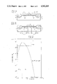
- a gate oxide film 4 is formed at a thickness of about 500 ⁇ on a surface portion of a p-type Si substrate 3 having an impurity concentration of about 10 15 atm/cm 3 .
- the gate oxide film 4 is exposed and surrounded by a field isolation oxide film 1 and a p + -type channel stopper region 2.
- a polycrystalline Si gate electrode 5 is formed on the gate oxide film 4 to a thickness of about 3000 ⁇ 4000 ⁇ ; thereafter arsenic ions (As + are implanted with a dosage of about 4 ⁇ 10 15 atm/cm 2 at an energy in the range of 100 ⁇ 150 KeV, for example 120 KeV, to the surface of the p-type Si substrate 3 through the gate oxide film 4 with the gate electrode 5 used as the mask (where 6' is the As + implanting region).
- FIG. 2 is a graph of an As concentration profile of the As implanting region thus formed.
- the curve shows the concentration of As vs. depth
- S is metallurgical solid solubility at 1100° C.
- EAS is electrically active solubility
- SiO 2 denotes a gate oxide film region
- Si denotes a p-type Si substrate region.
- the concentration of As at the peak value is larger than the electrically active solubility.
- As is redistributed by a thermal treatment in succeeding process steps and, as a result, the peak value of the concentration of As is lowered.
- FIG. 1(b) ia a cross-sectional view illustrating the condition after such annealing.
- 6 is the As diffused region (n+-type source/drain region) formed by annealing the As implanting region.
- the implanted As is diffused by the annealing process, so that the As diffused region (source/drain region) 6 is formed to a depth (d) of about 4000 ⁇ .
- the high temperature-heated annealing method has been accompanied by the problem that the lateral diffusion changes in dimension because the concentration profile of As in the diffused region cannot be controlled strictly, and element characteristics fluctuate due to the change in the length of the channel of the MIS type transistor.
- An example of a method which has been attempted in order to alleviate the above problems is the shallow formation of a diffused region. In this case, however, the total amount of As in the diffused region runs short and accordingly the desired low sheet resistance value cannot be obtained.
- Another example of a method which has been conducted is where the ion-implanted impurity is irradiated with an energy beam and is activated without any substantial redistribution of impurity. When redistribution of the impurity does not occur, the impurity does not expand laterally during the annealing process. However, an impurity implanted in such a concentration as to exceed the electrically active solubility is not activated because it is never reduced to a concentration lower than the electrically active solubility by redistribution. Nevertheless, if the ion implantation method is used, such a large amount of impurity must be implanted that the peak concentration exceeds the electrically active solubility, in order to obtain the low sheet resistance which is usually desired in an MIS type semiconductor
- a primary object of the present invention is to provide a method of forming an impurity region for a MIS type device having a desired low sheet resistance, without causing lateral diffusion of the impurity.
- Another object of the present invention is to prevent any adverse effects on the characteristics of the MIS type device caused by impurity concentrations exceeding the electrically active solubility.
- a method of manufacturing an MIS type semiconductor device having an impurity region formed in a semiconductor device comprising the steps of: implanting ions of an impurity into the semiconductor substrate with a plurality of varied implantation energies and with an implantation dosage to form the impurity region, the energies and the dosage being selected to provide an impurity distribution in the region having a peak concentration which does not exceed the electrically active solubility of the impurity; and irradiating the impurity region with an energy beam to render the implanted impurity in the region electrically active without any substantial redistribution of the impurity.
- the impurity is arsenic
- the electrically active solubility is 6 ⁇ 10 20 atm/cm 3
- a light beam emitted from a xenon lamp, a laser beam or an electron beam can be used as the energy beam.
- FIGS. 1(a) and 1(b) are cross-sectional views of a semiconductor substrate during the manufacturing process for an MIS type semiconductor device according to the prior art
- FIG. 2 is a graph indicating a prior art concentration profile for arsenic obtained by implanting arsenic ions
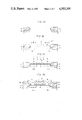
- FIGS. 3(a) through 3(d) are cross-sectional views of a semiconductor substrate during the manufacturing process for the MIS type semiconductor device according to the preferred embodiment of the present invention
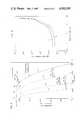
- FIG. 4 is a graph of the concentration profile for arsenic obtained by ion implantation of arsenic in accordance with the preferred embodiment of the present invention.
- FIG. 5 is a graph indicating the leakage current characteristic of a PN junction formed by the arsenic ion implantation process of the present invention.
- FIGS. 3(a) through 3(d) A preferred embodiment of the present invention will be explained in detail by referring to the cross-sectional view of a substrate during the manufacturing process as shown in FIGS. 3(a) through 3(d), and to the arsenic (As) concentration profile (FIG. 4) of an As implanted region of the same embodiment.
- As arsenic
- a substrate is prepared by a conventional method, wherein a field isolation oxide film 12 and a p + -type channel stopper region 13 are formed on a surface of a p-type silicon (Si) substrate 11, with an impurity concentration of about 10 15 atm/cm 3 .
- a gate oxide film 14 is formed to a thickness, for example, of about 500 ⁇ on the exposed surface of the p-type Si substrate 11 by an ordinary thermal oxidation method, and a polycrystalline Si gate electrode 15 is formed on the gate oxide film 14 by an ordinary chemical vapor deposition or patterning process.
- the As ion implantations are sequentially carried out under the following four kinds of conditions: (1) implantation energy of 110 KeV and dosage of 6 ⁇ 10 14 atm/cm 2 ; (2) implantation energy of 160 KeV and dosage of 7 ⁇ 10 14 atm/cm 2 ; (3) implantation energy of 240 KeV and dosage of 9.5 ⁇ 10 14 atm/cm 2 ; and (4) implantation energy of 320 KeV and dosage of 2.2 ⁇ 10 15 atm/cm 2 .
- an impurity-implanted region can be formed, wherein the peak concentration of the implanted As profile does not exceed the electrically active solubility of 6 ⁇ 10 20 atm/cm 3 .
- the field isolation oxide film 12 and the polycrystalline Si gate electrode 15 function as the implantation mask, and the arsenic (As) is implanted in the surface of p-type Si substrate 11 through the gate oxide film 14 (where 16' is the As + -implanted region).
- solid curve A indicates the profile of the total concentration of As in the p-type Si substrate 11 to which the As is implanted in multiple steps under the four kinds of implantation conditions.
- the vertical axis indicates the concentration of As, while the horizontal axis indicates the depth from the Si substrate surface.
- the dotted line curves A 1 through A 4 respectively indicate the concentration profile of As individually implanted under the respective conditions.
- the condition of the multiple implantation is preset so that the As concentration profile after multiple implantation does not exceed the electrically active solubility (EAS) in silicon at the peak value, since the EAS of As is about 2.5 ⁇ 10 20 atm/cm 3 .
- EAS electrically active solubility
- the junction depth is almost 4000 ⁇ .
- a light beam having an intensity of 26 J/cm 2 is irradiated for a short period of about 400 ⁇ s onto the As + -implanted region under the condition that the substrate is preheated, for example, up to 450° to 550° C. by a heater in an underlying substrate holder, so that the implanted As is activated without any substantial redistribution.
- a xenon flash lamp, etc. may be used as the light source.
- As-implanted regions 16a and 16b, at a depth of about 4000 ⁇ for N + -type source/drain regions are formed as shown in FIG. 3(c).
- the sheet resistance of the As-implanted regions 16a and 16b processed by the light irradiation annealing is as low as 20 ⁇ 30 ohms, substantially the same as the value obtained by the existing high temperature annealing method. Moreover, since the As is not redistributed during the light irradiation annealing process, the thus formed impurity region does not expand in the lateral direction from the edge of mask 17. Therefore, diffusion of impurity in the lateral direction from the mask edge in the present invention is kept within 0.1 ⁇ m which is inevitably introduced by the implantation of As + .
- FIG. 5 is the leakage current characteristic of the PN junction between the N + -type region thus formed and the p-type substrate under the reverse bias.
- the horizontal axis indicates bias voltage, while the vertical axis indicates the leakage current, and curve B shows the characteristic of the PN junction formed in this embodiment.
- the curve C shows the characteristic of a PN junction formed for comparison.
- This sample for comparison has been formed by a single As ion implantation with implantation energy of 200 KeV and dosage of 1 ⁇ 10 16 atm/cm 3 .
- the substrate used, annealing, and other conditions are the same as those for the embodiment of the invention.
- the resultant sheet resistance of the As-implanted region is about 30 ohms and this is almost the same as that of the embodiment.
- the leakage current is about double compared to the embodiment.
- the As region formed by the method of the above embodiment of the present invention has a much improved leakage current characteristic.
- the insulating layer 18 is formed on the substrate by a conventional method, an electrode window is formed in the insulating film and the source/drain wirings 19a, 19b are formed, thus completing an n-channel MIS-IC.
- a dosage of As + is adjusted to a value near its electrically active solubility in order to lower the sheet resistance as much as possible, but when a higher sheet resistance is acceptable, the total dosage is naturally selected to be lower.
- the present invention has been explained with reference to the source/drain regions in the above embodiment, but the method of this invention can also be applied to form wiring regions, such as bit wiring consisting of an impurity introduced region substrate as well.
- Phosphorous (P) and boron (B), in addition to As, can be used as the impurity to be implanted.
- the energy beam used to anneal for activation can be any energy beam (e.g., a laser beam, an electron beam, etc.) which is capable of instantly heating the substrate by irradiation.
- the method of the present invention when forming an impurity region having a low sheet resistance by using an ion implantation method, lateral diffusion of the impurity region and fluctuation in the size of the region are minimized. Therefore, the method of this invention is very effective for achieving high integration density and equalization of characteristics in a semiconductor device.
Abstract
Description
Claims (14)
Applications Claiming Priority (2)
| Application Number | Priority Date | Filing Date | Title |
|---|---|---|---|
| JP57-108003 | 1982-06-23 | ||
| JP57108003A JPS59920A (en) | 1982-06-23 | 1982-06-23 | Manufacture of semiconductor device |
Publications (1)
| Publication Number | Publication Date |
|---|---|
| US4502205A true US4502205A (en) | 1985-03-05 |
Family
ID=14473515
Family Applications (1)
| Application Number | Title | Priority Date | Filing Date |
|---|---|---|---|
| US06/505,976 Expired - Lifetime US4502205A (en) | 1982-06-23 | 1983-06-20 | Method of manufacturing an MIS type semiconductor device |
Country Status (4)
| Country | Link |
|---|---|
| US (1) | US4502205A (en) |
| EP (1) | EP0097533B1 (en) |
| JP (1) | JPS59920A (en) |
| DE (1) | DE3369426D1 (en) |
Cited By (16)
| Publication number | Priority date | Publication date | Assignee | Title |
|---|---|---|---|---|
| US4584763A (en) * | 1983-12-15 | 1986-04-29 | International Business Machines Corporation | One mask technique for substrate contacting in integrated circuits involving deep dielectric isolation |
| US4617066A (en) * | 1984-11-26 | 1986-10-14 | Hughes Aircraft Company | Process of making semiconductors having shallow, hyperabrupt doped regions by implantation and two step annealing |
| US4621411A (en) * | 1984-09-28 | 1986-11-11 | Texas Instruments Incorporated | Laser-enhanced drive in of source and drain diffusions |
| US4692992A (en) * | 1986-06-25 | 1987-09-15 | Rca Corporation | Method of forming isolation regions in a semiconductor device |
| US4697333A (en) * | 1985-02-20 | 1987-10-06 | Kabushiki Kaisha Toshiba | Method of manufacturing a semiconductor device using amorphous silicon as a mask |
| US4717684A (en) * | 1985-02-01 | 1988-01-05 | Hitachi, Ltd. | Semiconductor integrated circuit device |
| US4732868A (en) * | 1987-03-30 | 1988-03-22 | Eastman Kodak Company | Method of manufacture of a uniphase CCD |
| US4784968A (en) * | 1984-08-22 | 1988-11-15 | Hitachi, Ltd. | Process for manufacturing a semiconductor device having MIS-type field effect transistors with impurity region below the gate electrode |
| US5436484A (en) * | 1983-12-26 | 1995-07-25 | Hitachi, Ltd. | Semiconductor integrated circuit device having input protective elements and internal circuits |
| US5610089A (en) * | 1983-12-26 | 1997-03-11 | Hitachi, Ltd. | Method of fabrication of semiconductor integrated circuit device |
| US5933733A (en) * | 1994-06-23 | 1999-08-03 | Sgs-Thomson Microelectronics, S.R.L. | Zero thermal budget manufacturing process for MOS-technology power devices |
| US5966605A (en) * | 1997-11-07 | 1999-10-12 | Advanced Micro Devices, Inc. | Reduction of poly depletion in semiconductor integrated circuits |
| US6146953A (en) * | 1998-04-20 | 2000-11-14 | Hyundai Electronics Industries Co., Ltd. | Fabrication method for mosfet device |
| US6500704B1 (en) * | 1995-07-03 | 2002-12-31 | Sanyo Electric Co., Ltd | Semiconductor device, display device and method of fabricating the same |
| US20040121567A1 (en) * | 2002-09-06 | 2004-06-24 | Nat'l Inst. Of Advan. Industrial Science And Tech. | Doping method and semiconductor device fabricated using the method |
| US6790714B2 (en) | 1995-07-03 | 2004-09-14 | Sanyo Electric Co., Ltd. | Semiconductor device, display device and method of fabricating the same |
Families Citing this family (4)
| Publication number | Priority date | Publication date | Assignee | Title |
|---|---|---|---|---|
| DE3342773A1 (en) * | 1983-11-25 | 1985-06-05 | Siemens AG, 1000 Berlin und 8000 München | Process for producing MOS field-effect transistors with high dielectric strength and with a gentle concentration profile at the drain junction |
| EP0164605B1 (en) * | 1984-05-17 | 1990-02-28 | Kabushiki Kaisha Toshiba | Method of manufacturing nonvolatile semiconductor eeprom device |
| FR2566583B1 (en) * | 1984-06-22 | 1986-09-19 | Thomson Csf | METHOD FOR MANUFACTURING AT LEAST ONE THIN FILM FIELD-EFFECT TRANSISTOR, AND TRANSISTOR OBTAINED BY THIS METHOD |
| US5789802A (en) * | 1996-06-21 | 1998-08-04 | Advanced Micro Devices, Inc. | Dopant profile spreading for arsenic source/drain |
Citations (4)
| Publication number | Priority date | Publication date | Assignee | Title |
|---|---|---|---|---|
| US4116717A (en) * | 1976-12-08 | 1978-09-26 | The United States Of America As Represented By The Secretary Of The Air Force | Ion implanted eutectic gallium arsenide solar cell |
| JPS54106180A (en) * | 1978-02-08 | 1979-08-20 | Nippon Telegr & Teleph Corp <Ntt> | Manufacture of semiconductor integrated circuit |
| JPS55107229A (en) * | 1979-02-08 | 1980-08-16 | Chiyou Lsi Gijutsu Kenkyu Kumiai | Method of manufacturing semiconductor device |
| US4331485A (en) * | 1980-03-03 | 1982-05-25 | Arnon Gat | Method for heat treating semiconductor material using high intensity CW lamps |
Family Cites Families (3)
| Publication number | Priority date | Publication date | Assignee | Title |
|---|---|---|---|---|
| FR2236271A1 (en) * | 1973-06-19 | 1975-01-31 | Anvar | Method of semiconductor junction fabrication - uses localised laser irradiation followed by reheating |
| JPS5839376B2 (en) * | 1978-10-30 | 1983-08-30 | 富士通株式会社 | Ion implantation method |
| JPS55128823A (en) * | 1979-03-28 | 1980-10-06 | Hitachi Ltd | Semiconductor device and manufacture thereof |
-
1982
- 1982-06-23 JP JP57108003A patent/JPS59920A/en active Pending
-
1983
- 1983-06-20 US US06/505,976 patent/US4502205A/en not_active Expired - Lifetime
- 1983-06-22 EP EP83303587A patent/EP0097533B1/en not_active Expired
- 1983-06-22 DE DE8383303587T patent/DE3369426D1/en not_active Expired
Patent Citations (4)
| Publication number | Priority date | Publication date | Assignee | Title |
|---|---|---|---|---|
| US4116717A (en) * | 1976-12-08 | 1978-09-26 | The United States Of America As Represented By The Secretary Of The Air Force | Ion implanted eutectic gallium arsenide solar cell |
| JPS54106180A (en) * | 1978-02-08 | 1979-08-20 | Nippon Telegr & Teleph Corp <Ntt> | Manufacture of semiconductor integrated circuit |
| JPS55107229A (en) * | 1979-02-08 | 1980-08-16 | Chiyou Lsi Gijutsu Kenkyu Kumiai | Method of manufacturing semiconductor device |
| US4331485A (en) * | 1980-03-03 | 1982-05-25 | Arnon Gat | Method for heat treating semiconductor material using high intensity CW lamps |
Non-Patent Citations (2)
| Title |
|---|
| P. Siffert, in Proceedings, 4th European Community Photovoltaic Solar Energy Conf., Stresa, Italy, May 1982, Reidel Pub. Co., pp. 901 918. * |
| P. Siffert, in Proceedings, 4th European Community Photovoltaic Solar Energy Conf., Stresa, Italy, May 1982, Reidel Pub. Co., pp. 901-918. |
Cited By (19)
| Publication number | Priority date | Publication date | Assignee | Title |
|---|---|---|---|---|
| US4584763A (en) * | 1983-12-15 | 1986-04-29 | International Business Machines Corporation | One mask technique for substrate contacting in integrated circuits involving deep dielectric isolation |
| US5436484A (en) * | 1983-12-26 | 1995-07-25 | Hitachi, Ltd. | Semiconductor integrated circuit device having input protective elements and internal circuits |
| US5610089A (en) * | 1983-12-26 | 1997-03-11 | Hitachi, Ltd. | Method of fabrication of semiconductor integrated circuit device |
| US5436483A (en) * | 1983-12-26 | 1995-07-25 | Hitachi, Ltd. | Semiconductor integrated circuit device having a first MISFET of an output buffer circuit and a second MISFET of an internal circuit |
| US4784968A (en) * | 1984-08-22 | 1988-11-15 | Hitachi, Ltd. | Process for manufacturing a semiconductor device having MIS-type field effect transistors with impurity region below the gate electrode |
| US4621411A (en) * | 1984-09-28 | 1986-11-11 | Texas Instruments Incorporated | Laser-enhanced drive in of source and drain diffusions |
| US4617066A (en) * | 1984-11-26 | 1986-10-14 | Hughes Aircraft Company | Process of making semiconductors having shallow, hyperabrupt doped regions by implantation and two step annealing |
| US4717684A (en) * | 1985-02-01 | 1988-01-05 | Hitachi, Ltd. | Semiconductor integrated circuit device |
| US4697333A (en) * | 1985-02-20 | 1987-10-06 | Kabushiki Kaisha Toshiba | Method of manufacturing a semiconductor device using amorphous silicon as a mask |
| US4692992A (en) * | 1986-06-25 | 1987-09-15 | Rca Corporation | Method of forming isolation regions in a semiconductor device |
| US4732868A (en) * | 1987-03-30 | 1988-03-22 | Eastman Kodak Company | Method of manufacture of a uniphase CCD |
| US5933733A (en) * | 1994-06-23 | 1999-08-03 | Sgs-Thomson Microelectronics, S.R.L. | Zero thermal budget manufacturing process for MOS-technology power devices |
| US6500704B1 (en) * | 1995-07-03 | 2002-12-31 | Sanyo Electric Co., Ltd | Semiconductor device, display device and method of fabricating the same |
| US6790714B2 (en) | 1995-07-03 | 2004-09-14 | Sanyo Electric Co., Ltd. | Semiconductor device, display device and method of fabricating the same |
| US7084052B2 (en) | 1995-07-03 | 2006-08-01 | Sanyo Electric Co., Ltd. | Semiconductor device, display device and method of fabricating the same |
| US5966605A (en) * | 1997-11-07 | 1999-10-12 | Advanced Micro Devices, Inc. | Reduction of poly depletion in semiconductor integrated circuits |
| US6146953A (en) * | 1998-04-20 | 2000-11-14 | Hyundai Electronics Industries Co., Ltd. | Fabrication method for mosfet device |
| US20040121567A1 (en) * | 2002-09-06 | 2004-06-24 | Nat'l Inst. Of Advan. Industrial Science And Tech. | Doping method and semiconductor device fabricated using the method |
| US7138688B2 (en) * | 2002-09-06 | 2006-11-21 | National Institute Of Advanced Industrial Science And Technology | Doping method and semiconductor device fabricated using the method |
Also Published As
| Publication number | Publication date |
|---|---|
| EP0097533A2 (en) | 1984-01-04 |
| EP0097533B1 (en) | 1987-01-21 |
| JPS59920A (en) | 1984-01-06 |
| EP0097533A3 (en) | 1985-05-29 |
| DE3369426D1 (en) | 1987-02-26 |
Similar Documents
| Publication | Publication Date | Title |
|---|---|---|
| US4502205A (en) | Method of manufacturing an MIS type semiconductor device | |
| US5899732A (en) | Method of implanting silicon through a polysilicon gate for punchthrough control of a semiconductor device | |
| US6331468B1 (en) | Formation of integrated circuit structure using one or more silicon layers for implantation and out-diffusion in formation of defect-free source/drain regions and also for subsequent formation of silicon nitride spacers | |
| US6184112B1 (en) | Method of forming a MOSFET transistor with a shallow abrupt retrograde dopant profile | |
| US7217627B2 (en) | Semiconductor devices having diffusion barrier regions and halo implant regions and methods of fabricating the same | |
| US5552332A (en) | Process for fabricating a MOSFET device having reduced reverse short channel effects | |
| US7605064B2 (en) | Selective laser annealing of semiconductor material | |
| US5976956A (en) | Method of controlling dopant concentrations using transient-enhanced diffusion prior to gate formation in a device | |
| US5943595A (en) | Method for manufacturing a semiconductor device having a triple-well structure | |
| US4038107A (en) | Method for making transistor structures | |
| EP1068637A1 (en) | Reduced channel length lightly doped drain transistor using a sub-amorphous large tilt angle implant to provide enhanced lateral diffusion | |
| US4243433A (en) | Forming controlled inset regions by ion implantation and laser bombardment | |
| JPH08203842A (en) | Manufacture of semiconductor device | |
| US6013566A (en) | Method of forming a doped region in a semiconductor substrate | |
| US6475885B1 (en) | Source/drain formation with sub-amorphizing implantation | |
| US5677213A (en) | Method for forming a semiconductor device having a shallow junction and a low sheet resistance | |
| JPS6362227A (en) | Correction of characteristics of p-type dopant by other p-type dopant | |
| US4621413A (en) | Fabricating a semiconductor device with reduced gate leakage | |
| US5844276A (en) | CMOS integrated circuit and method for implanting NMOS transistor areas prior to implanting PMOS transistor areas to optimize the thermal diffusivity thereof | |
| US20030082922A1 (en) | Method of fabricating integrated circuit having shallow junction | |
| WO1985000694A1 (en) | Shallow-junction semiconductor devices | |
| US4621411A (en) | Laser-enhanced drive in of source and drain diffusions | |
| US5874343A (en) | CMOS integrated circuit and method for forming source/drain areas prior to forming lightly doped drains to optimize the thermal diffusivity thereof | |
| US20010018258A1 (en) | Method for fabricating semiconductor device | |
| KR100671594B1 (en) | Method of manufacturing a transistor having a shallow junction in a semiconductor device |
Legal Events
| Date | Code | Title | Description |
|---|---|---|---|
| AS | Assignment |
Owner name: FUJITSU LIMITED, 1015, KAMIKODANAKA, NAKAHARA-KU, Free format text: ASSIGNMENT OF ASSIGNORS INTEREST.;ASSIGNOR:YAHANO, TOSHI;REEL/FRAME:004144/0355 Effective date: 19830613 |
|
| STCF | Information on status: patent grant |
Free format text: PATENTED CASE |
|
| CC | Certificate of correction | ||
| FEPP | Fee payment procedure |
Free format text: PAYOR NUMBER ASSIGNED (ORIGINAL EVENT CODE: ASPN); ENTITY STATUS OF PATENT OWNER: LARGE ENTITY |
|
| FPAY | Fee payment |
Year of fee payment: 4 |
|
| FPAY | Fee payment |
Year of fee payment: 8 |
|
| FEPP | Fee payment procedure |
Free format text: PAYOR NUMBER ASSIGNED (ORIGINAL EVENT CODE: ASPN); ENTITY STATUS OF PATENT OWNER: LARGE ENTITY Free format text: PAYER NUMBER DE-ASSIGNED (ORIGINAL EVENT CODE: RMPN); ENTITY STATUS OF PATENT OWNER: LARGE ENTITY |
|
| FPAY | Fee payment |
Year of fee payment: 12 |