US4509140A - Data transmitting link - Google Patents
Data transmitting link Download PDFInfo
- Publication number
- US4509140A US4509140A US06/391,778 US39177882A US4509140A US 4509140 A US4509140 A US 4509140A US 39177882 A US39177882 A US 39177882A US 4509140 A US4509140 A US 4509140A
- Authority
- US
- United States
- Prior art keywords
- memory
- ports
- local
- access
- data
- Prior art date
- Legal status (The legal status is an assumption and is not a legal conclusion. Google has not performed a legal analysis and makes no representation as to the accuracy of the status listed.)
- Expired - Lifetime
Links
- 230000015654 memory Effects 0.000 claims abstract description 143
- 238000004891 communication Methods 0.000 claims abstract description 7
- 230000009977 dual effect Effects 0.000 claims abstract description 6
- 238000012545 processing Methods 0.000 claims description 7
- 125000004122 cyclic group Chemical group 0.000 claims description 3
- 230000004044 response Effects 0.000 claims description 3
- 239000000872 buffer Substances 0.000 description 16
- 230000005540 biological transmission Effects 0.000 description 10
- 238000010586 diagram Methods 0.000 description 8
- 230000000694 effects Effects 0.000 description 4
- 101000685663 Homo sapiens Sodium/nucleoside cotransporter 1 Proteins 0.000 description 3
- 102100023116 Sodium/nucleoside cotransporter 1 Human genes 0.000 description 3
- 241001061076 Melanonus zugmayeri Species 0.000 description 2
- 101100108340 Solanum commersonii SCM1 gene Proteins 0.000 description 2
- 101100495267 Saccharomyces cerevisiae (strain ATCC 204508 / S288c) CDC25 gene Proteins 0.000 description 1
- 239000013078 crystal Substances 0.000 description 1
- 238000013461 design Methods 0.000 description 1
- 230000006870 function Effects 0.000 description 1
- 230000010365 information processing Effects 0.000 description 1
- 238000000034 method Methods 0.000 description 1
- 238000012360 testing method Methods 0.000 description 1
Images


Classifications
-
- G—PHYSICS
- G06—COMPUTING; CALCULATING OR COUNTING
- G06F—ELECTRIC DIGITAL DATA PROCESSING
- G06F13/00—Interconnection of, or transfer of information or other signals between, memories, input/output devices or central processing units
- G06F13/14—Handling requests for interconnection or transfer
- G06F13/16—Handling requests for interconnection or transfer for access to memory bus
- G06F13/18—Handling requests for interconnection or transfer for access to memory bus based on priority control
Definitions
- This invention relates to information processing and more particularly to forwarding data from one station of a data processing network to another.
- the invention features, in a communication link, a memory unit including a common section accessible to all ports of the link and a plurality of local sections each associated with one of the ports and accessible to its associated port, and no other port; interconnections including a dual memory bus with a common bus subsystem providing access to the common memory section and a local bus subsystem providing access to the plurality of local memory sections, the common and local subsystems being constructed to enable concurrent independent use; ports including decoding circuitry which receives signals from its associated station and in response thereto emits signals distinctively indicating the need for access to the memory common section or its associated memory local section, which emitted signals are transmitted to said memory priority circuitry; memory priority circuitry supplying timed signals which designate for each memory operating cycle the one of the ports which may have access to the memory, access being made available to the several ports in cyclic order, and futher designating for each memory cycle one of the ports for current service and responding to request signals indicating needs for memory access, and if the currently designated port requests memory access, enabling the currently designated port
- the invention may additionally feature circuitry for processing access requests for a succeeding memory operation while a current memory operation is in progress and for effecting a memory operation rate such that a time interval expressed by (n+1) T+L is less than the minimum time required to transmit one byte of data to one of said ports, n being the number of ports, T being the memory operating cycle period, and L being the overlap period during which memory requests are being processed for a succeeding memory operation while a current operation is in progress.
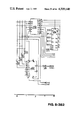
- FIG. 1 shows in block diagram a data processing network in which a communication link according to the invention is used.
- FIG. 2 shows in block diagram form the communication link of FIG. 1.
- FIG. 3 shows in block diagram form the processor which is a part of the link of FIG. 2.
- FIG. 4 shows in block diagram form the memory unit which is a part of the link of FIG. 2.
- FIG. 5 shows in block diagram form one of the data ports of the link of FIG. 2.
- FIGS. 6-1A, 6-1B, 6-1C, 6-2A, 6-2B, 6-2C, 6-3A, 6-3B, and 6-3C are in the aggregate the schematic wiring diagram of the processor of FIG. 3.
- FIGS. 7-1A, 7-1B, 7-1C, 7-2A, 7-2B, and 7-2C are in the aggregate the schematic wiring diagram of the memory unit of FIG. 4.
- FIGS. 8-1A, 8-1B, 8-1C, 8-2A, 8-2B, 8-2C, 8-3A, 8-3B, and 8-3C are in the aggregate the schematic wiring diagram of the data port of FIG. 5.
- FIGS. 6-1 through 3, 7-1 through 2 and 8-1 through 3 should be considered as reconstituted by placing the -A, -B, and -C parts side by side to form a single figure.
- a number of connecting leads are not shown in full but are terminated with an arrowhead and a notation identifying the lead and the location on the drawing where it goes, the location being given by a first number, a letter, and a second number all in parenthesis.
- the first number indicates the drawing part
- the letter and the second number indicates, by reference to the edge marking, the place on the sheet.
- the arrowhead and arrowtail thus coupled are to be considered as connected.
- data processing network 10 includes a communication link 12, according to the invention, linking four work stations 14-0, 14-1, 14-2, and 14-3, the work stations being connected to data ports 16-0, 16-1, 16-2, 16-3, respectively which are part of link 12.
- Link 12 includes data ports 16-0, 16-1, 16-2, 16-3, processor 18, memory unit 20, and power supply 22, with switch 24.
- Interconnections 26 connect together the ports, processor, memory unit, and power supply, and include a dual memory bus system 28 with a local memory bus subsystem 30 having a local address bus 32 and a local data bus 34, and a common memory bus subsystem 36 having a common address bus 38 and a common data bus 40.
- Interconnections 26 also include diagnostic bus 42 and other control leads.
- processor unit 18 includes a Z80 CPU L56 and a Z80 CTC L55, a local memory address buffer L54 connected to the local memory address bus 32, a local memory data-in buffer L84, and a local memory data-out buffer L85, both connected to local memory data bus 34, a common memory address buffer L51 and L52 connected to the common memory address bus 38 and a common data in buffer L89 and common data out buffer L90 both connected to the common data bus 40.
- the processor unit 18 additionally includes a start up memory 44 of elements L11 through L15 and L25 through L28, wherein there are 7K of programmable read only memory and 1K of random access memory.
- the processor also includes memory request/control circuitry 46 connecting through leads ZMRQ, ZMWT, ZCM, ZENC, ZENL, ZBS0, ZBS1 to memory unit 20.
- the processor unit includes circuitry 48 of conventional design dealing with diagnostic operations for detecting errors and other control functions which are shown in detail in FIGS. 6-1, 6-2, 6-3 but are not directly related to the subject invention and need not be discussed further.
- the data port 16-1 is shown as representative of the four identical ports 16-0, 16-1, 16-2, 16-3.
- the data port includes coax driver and receiver circuitry 50, which is connected by dual coax transmission lines 52-1 to an associated remote station, and decoding circuitry 53 which includes IC components L40, L41, L42, and L25.
- the data port also includes diagnostic and control circuitry 54 and memory request-control circuitry 56 connecting through leads SMRQ1, SMWT1, SCM1, SENC1, SENL1, and SMAK1 to memory unit 20.
- the data port additionally includes status buffer L64, local memory address buffer L58 connecting with local address bus 32, local memory data-in buffer L62 and local memory data-out buffer L80, both connecting with local data bus 34, common memory address buffer L59, L78 connecting with common address bus 38, and common memory data-in buffer L63 and common memory data-out buffer L81 both connecting with common memory data bus 40.
- memory unit 20 includes a common section 58 with a memory controller 60, and refresh circuitry 66, local memory sections 62 with local memory controller 64, memory priority circuitry 68 and timing circuitry 70.
- Common memory 58 has a 9 bit by 64K capacity and its 16 address bits connect to common address bus 38, and its 8 data bits and one parity bit to common data bus 40.
- Local memory 62 has a 9 bit by 1K capacity and its data bits connect to local memory bus 54. Of the 10 addressing bits of the local memory 62 eight (LA0-LA7) connect to local address bus 32. The remaining 2 addressing bits are connected through leads B20 and BS1 to memory priority circuitry 68.
- Local memory 62 is thus effectively divided into 4 sections with data entering from local data bus 34 entered into a memory section in accordance with the signals on leads BS0 and BS1 from memory priority circuitry 68.
- Timing circuitry 70 includes a crystal oscillator operating with a period 58 ns from which are derived various timing signals for synchronizing the system. Among these are signals emitted on lead CNT0 with period 936 ns and on lead CNT1 with period 1872 ns which are used to control the time sharing of the four ports.
- Memory priority circuitry 68 connects through control leads 72-0, 72-1, 72-2, 72-3, to ports 16-0, 16-1, 16-2, 16-3, and to processor 18, through leads 72-Z, ZBS0 and ZBS1. It also connects with the local and common memories, the refresh circuitry and the timing circuitry.
- each port of the link transfers serial data to or from its corresponding station at a rate of 4.27 megabits per second over the double coaxial cable 52-1 (using port 16-1 as exemplary).
- the transmission character consists of 11 bits: a start bit (one) eight data bits (transmitted most significant bit first), an odd parity bit, and a stop bit (zero).
- start bit one
- odd parity bit an odd parity bit
- stop bit zero
- the protocol between the link and the stations calls for the station to initiate all transmissions. When such a signal is transmitted to the port it is stripped of its start and stop bits, parallelized and parity checked.
- the protocol admits of six commands:
- the first following transmission character will contain the 8-bit high order address of the memory site, the second following character will contain the 8-bit lower address, and the third following character will contain the 8-bit data byte.
- the first following transmission character will contain the high order address and the second following character the low order address of the byte to be read.
- the first following transmission character will contain the high order address and the second following will contain the low order address of the first of the 256 bytes to be read.
- the parallelized byte is entered into decoding buffer L41, into memory-out buffers L80, L81 and address buffers L58, L59, L62.
- Decode circuitry decodes the command, counts successive bytes as required to interpret whether a byte is a high order address, a low order address, a data byte, or a command and decodes the address to distinguish whether the address is in local or common memory. (The lowest 256 addresses are assigned to local memory).
- the decode circuitry outputs on leads SMRQ1, SMWT1, and SCM1 signals indicating respectively whether memory is needed or not, whether read or write is required, and whether common or local memory is required.
- the CPU Concurrently with the transmission flowing between each of the ports and its associated station, the CPU is engaged in activities for management of the link and its data space under control of the program in a portion of the common memory and these activities generate requirements to have access to the common and to each of the local memory sections.
- Memory request control circuitry 46 in the CPU unit indicates its needs for memory access by signals on lead ZMRQZMWT, ZCM in a manner directly analogous to similar signals from the ports as described above.
- the memory request circuitry generates signals on leads ZBS0 and ZBS1 which indicate which of the four sections of local memory are needed.
- the priority circuitry also receives signals from the timing circuitry 70 on lead ⁇ R indicating a need to refresh the dynamic common memory and signals on CNT0 and CTN1 which designate the particular one of the ports to have its turn to be served.
- the logic of the priority circuits designate the access to the memory buses for the next memory cycle in response to input signals according to the following priorities:
- the memory priority circuitry emits signals on leads SENC-1, SENL-1, and SMAK-1 to port 16-1 and analogous ones to other ports and the CPU unit to effect the switching to the buses in accordance with the priority decision as described above.
- the priority circuitry generates signals which designate the particular section of the local memory to be addressed by generating address bits emitted on leads BS0 and BS1. When a particular port is given access to the local memory, these two bits are derived from the signals on CNT0 and CNT1 which indicate the port on turn. When the CPU is given access to the local memory the two address bits are derived from the signals emitted by the CPU on leads ZBS0 and ZBS1.
- a single operation of the memory includes a period of 117 ns for resolving the bus priorities followed by a period of 468 ns for actual memory access.
- the successive operations are overlapped, with priority resolution for a succeeding cycle going forward while memory entry is in progress, so that the memory cyclic period is 468 ns.
- a wait of 4 cycles or 1872 ns as the priority circuitry serviced the other ports and returned to the request of the particular port. Then there would be the intervals of 117 ns and 468 ns while its memory operation was processed--a total of 2457 ns.
- the maximum rate at which a port needs memory access is however, 389 MHz or 1.566 MHz for the aggregate of the 4 ports.
- the memory access requirements for the refresh logic is 0.064 MHz so that even with maximum port activity 0.52 MHz of memory access is available for the CPU, and in practice more than this because of the dual memory system.
- the start up of the link is not directly related to the invention and needs only cursory description. It is effected by turning on switch 24 of power supply 22.
- the application of power supplies to the equipment set gates in initial states and starts the CPU on a program at address 0000 in start-up memory 44.
- the program may go through various system test of if desired but in any case selects a station as a master station for implementation and sets a flag in the status register L64 of corresponding port indicating that the link is ready to be programmed.
- the master station has been periodically requesting a status report from the link and now for the first time receives a report that the link is ready for programming.
- the master station then enters the operating program into the common memory using the procedure as described above for entering data. After the program is entered the master station transmits the reset command and this transfers the CPU to the program just entered in the common memory.
- the system then begins its normal operations.
Abstract
Description
Claims (4)
Priority Applications (1)
| Application Number | Priority Date | Filing Date | Title |
|---|---|---|---|
| US06/391,778 US4509140A (en) | 1980-11-10 | 1982-06-24 | Data transmitting link |
Applications Claiming Priority (2)
| Application Number | Priority Date | Filing Date | Title |
|---|---|---|---|
| US20516480A | 1980-11-10 | 1980-11-10 | |
| US06/391,778 US4509140A (en) | 1980-11-10 | 1982-06-24 | Data transmitting link |
Related Parent Applications (1)
| Application Number | Title | Priority Date | Filing Date |
|---|---|---|---|
| US20516480A Continuation-In-Part | 1980-11-10 | 1980-11-10 |
Publications (1)
| Publication Number | Publication Date |
|---|---|
| US4509140A true US4509140A (en) | 1985-04-02 |
Family
ID=26900177
Family Applications (1)
| Application Number | Title | Priority Date | Filing Date |
|---|---|---|---|
| US06/391,778 Expired - Lifetime US4509140A (en) | 1980-11-10 | 1982-06-24 | Data transmitting link |
Country Status (1)
| Country | Link |
|---|---|
| US (1) | US4509140A (en) |
Cited By (22)
| Publication number | Priority date | Publication date | Assignee | Title |
|---|---|---|---|---|
| US4627018A (en) * | 1983-09-08 | 1986-12-02 | Sperry Corporation | Priority requestor accelerator |
| US4633434A (en) * | 1984-04-02 | 1986-12-30 | Sperry Corporation | High performance storage unit |
| US4649475A (en) * | 1984-04-02 | 1987-03-10 | Sperry Corporation | Multiple port memory with port decode error detector |
| US4654788A (en) * | 1983-06-15 | 1987-03-31 | Honeywell Information Systems Inc. | Asynchronous multiport parallel access memory system for use in a single board computer system |
| US4665483A (en) * | 1983-10-25 | 1987-05-12 | Honeywell Information Systems Italia | Data processing system architecture |
| US4674033A (en) * | 1983-10-24 | 1987-06-16 | British Telecommunications Public Limited Company | Multiprocessor system having a shared memory for enhanced interprocessor communication |
| US4716521A (en) * | 1983-07-13 | 1987-12-29 | Fujitsu Limited | Microcomputer |
| US4754394A (en) * | 1984-10-24 | 1988-06-28 | International Business Machines Corporation | Multiprocessing system having dynamically allocated local/global storage and including interleaving transformation circuit for transforming real addresses to corresponding absolute address of the storage |
| US4754399A (en) * | 1983-12-28 | 1988-06-28 | Hitachi, Ltd. | Data transfer control system for controlling data transfer between a buffer memory and input/output devices |
| US4853850A (en) * | 1985-09-10 | 1989-08-01 | Krass Jr James E | Vehicle computer diagnostic interface apparatus |
| USH696H (en) | 1984-07-03 | 1989-10-03 | Cpt Corporation | System for accessing shared resource device by intelligent user devices |
| US4901230A (en) * | 1983-04-25 | 1990-02-13 | Cray Research, Inc. | Computer vector multiprocessing control with multiple access memory and priority conflict resolution method |
| US5142638A (en) * | 1989-02-07 | 1992-08-25 | Cray Research, Inc. | Apparatus for sharing memory in a multiprocessor system |
| US5146565A (en) * | 1986-07-18 | 1992-09-08 | Intel Corporation | I/O Control system having a plurality of access enabling bits for controlling access to selective ports of an I/O device |
| US5159674A (en) * | 1982-11-09 | 1992-10-27 | Siemens Aktiengesellschaft | Method for supplying microcommands to multiple independent functional units having a next microcommand available during execution of a current microcommand |
| US5202970A (en) * | 1989-02-07 | 1993-04-13 | Cray Research, Inc. | Method for sharing memory in a multiprocessor system |
| US5206952A (en) * | 1990-09-12 | 1993-04-27 | Cray Research, Inc. | Fault tolerant networking architecture |
| US5212631A (en) * | 1990-08-31 | 1993-05-18 | Allen-Bradley Company, Inc. | Programmable controller processor module having multiple program instruction execution sections |
| US5247637A (en) * | 1990-06-01 | 1993-09-21 | Cray Research, Inc. | Method and apparatus for sharing memory in a multiprocessor system |
| US5265005A (en) * | 1990-08-31 | 1993-11-23 | Allen-Bradley Company, Inc. | Processor for a programmable controller |
| US5367680A (en) * | 1990-02-13 | 1994-11-22 | International Business Machines Corporation | Rendering context manager for display adapters supporting multiple domains |
| US5584010A (en) * | 1988-11-25 | 1996-12-10 | Mitsubishi Denki Kabushiki Kaisha | Direct memory access control device and method in a multiprocessor system accessing local and shared memory |
Citations (4)
| Publication number | Priority date | Publication date | Assignee | Title |
|---|---|---|---|---|
| US3530438A (en) * | 1965-12-13 | 1970-09-22 | Sperry Rand Corp | Task control |
| US4071887A (en) * | 1975-10-30 | 1978-01-31 | Motorola, Inc. | Synchronous serial data adaptor |
| US4124891A (en) * | 1976-11-18 | 1978-11-07 | Honeywell Information Systems Inc. | Memory access system |
| US4164787A (en) * | 1977-11-09 | 1979-08-14 | Bell Telephone Laboratories, Incorporated | Multiple microprocessor intercommunication arrangement |
-
1982
- 1982-06-24 US US06/391,778 patent/US4509140A/en not_active Expired - Lifetime
Patent Citations (4)
| Publication number | Priority date | Publication date | Assignee | Title |
|---|---|---|---|---|
| US3530438A (en) * | 1965-12-13 | 1970-09-22 | Sperry Rand Corp | Task control |
| US4071887A (en) * | 1975-10-30 | 1978-01-31 | Motorola, Inc. | Synchronous serial data adaptor |
| US4124891A (en) * | 1976-11-18 | 1978-11-07 | Honeywell Information Systems Inc. | Memory access system |
| US4164787A (en) * | 1977-11-09 | 1979-08-14 | Bell Telephone Laboratories, Incorporated | Multiple microprocessor intercommunication arrangement |
Cited By (22)
| Publication number | Priority date | Publication date | Assignee | Title |
|---|---|---|---|---|
| US5159674A (en) * | 1982-11-09 | 1992-10-27 | Siemens Aktiengesellschaft | Method for supplying microcommands to multiple independent functional units having a next microcommand available during execution of a current microcommand |
| US4901230A (en) * | 1983-04-25 | 1990-02-13 | Cray Research, Inc. | Computer vector multiprocessing control with multiple access memory and priority conflict resolution method |
| US4654788A (en) * | 1983-06-15 | 1987-03-31 | Honeywell Information Systems Inc. | Asynchronous multiport parallel access memory system for use in a single board computer system |
| US4716521A (en) * | 1983-07-13 | 1987-12-29 | Fujitsu Limited | Microcomputer |
| US4627018A (en) * | 1983-09-08 | 1986-12-02 | Sperry Corporation | Priority requestor accelerator |
| US4674033A (en) * | 1983-10-24 | 1987-06-16 | British Telecommunications Public Limited Company | Multiprocessor system having a shared memory for enhanced interprocessor communication |
| US4665483A (en) * | 1983-10-25 | 1987-05-12 | Honeywell Information Systems Italia | Data processing system architecture |
| US4754399A (en) * | 1983-12-28 | 1988-06-28 | Hitachi, Ltd. | Data transfer control system for controlling data transfer between a buffer memory and input/output devices |
| US4633434A (en) * | 1984-04-02 | 1986-12-30 | Sperry Corporation | High performance storage unit |
| US4649475A (en) * | 1984-04-02 | 1987-03-10 | Sperry Corporation | Multiple port memory with port decode error detector |
| USH696H (en) | 1984-07-03 | 1989-10-03 | Cpt Corporation | System for accessing shared resource device by intelligent user devices |
| US4754394A (en) * | 1984-10-24 | 1988-06-28 | International Business Machines Corporation | Multiprocessing system having dynamically allocated local/global storage and including interleaving transformation circuit for transforming real addresses to corresponding absolute address of the storage |
| US4853850A (en) * | 1985-09-10 | 1989-08-01 | Krass Jr James E | Vehicle computer diagnostic interface apparatus |
| US5146565A (en) * | 1986-07-18 | 1992-09-08 | Intel Corporation | I/O Control system having a plurality of access enabling bits for controlling access to selective ports of an I/O device |
| US5584010A (en) * | 1988-11-25 | 1996-12-10 | Mitsubishi Denki Kabushiki Kaisha | Direct memory access control device and method in a multiprocessor system accessing local and shared memory |
| US5142638A (en) * | 1989-02-07 | 1992-08-25 | Cray Research, Inc. | Apparatus for sharing memory in a multiprocessor system |
| US5202970A (en) * | 1989-02-07 | 1993-04-13 | Cray Research, Inc. | Method for sharing memory in a multiprocessor system |
| US5367680A (en) * | 1990-02-13 | 1994-11-22 | International Business Machines Corporation | Rendering context manager for display adapters supporting multiple domains |
| US5247637A (en) * | 1990-06-01 | 1993-09-21 | Cray Research, Inc. | Method and apparatus for sharing memory in a multiprocessor system |
| US5212631A (en) * | 1990-08-31 | 1993-05-18 | Allen-Bradley Company, Inc. | Programmable controller processor module having multiple program instruction execution sections |
| US5265005A (en) * | 1990-08-31 | 1993-11-23 | Allen-Bradley Company, Inc. | Processor for a programmable controller |
| US5206952A (en) * | 1990-09-12 | 1993-04-27 | Cray Research, Inc. | Fault tolerant networking architecture |
Similar Documents
| Publication | Publication Date | Title |
|---|---|---|
| US4509140A (en) | Data transmitting link | |
| US4212057A (en) | Shared memory multi-microprocessor computer system | |
| US4523272A (en) | Bus selection control in a data transmission apparatus for a multiprocessor system | |
| AU663536B2 (en) | Bus control logic for computer system having dual bus architecture | |
| US4695952A (en) | Dual redundant bus interface circuit architecture | |
| US4394726A (en) | Distributed multiport memory architecture | |
| US6189062B1 (en) | Apparatus and method for address translation in bus bridge devices | |
| US4945473A (en) | Communications controller interface | |
| EP0184976B1 (en) | Apparatus for interfacing between at least one channel and at least one bus | |
| CA1307352C (en) | Shared memory controller arrangement | |
| US7412556B2 (en) | Method and system for master devices accessing slave devices | |
| US4695948A (en) | Bus to bus converter using a RAM for multiple address mapping | |
| JPH04257054A (en) | Inter-channel connecting apparatus | |
| JPS6336586B2 (en) | ||
| CA1178685A (en) | Data transmitting link | |
| US5444852A (en) | I/O device interface having buffer mapped in processor memory addressing space and control registers mapped in processor I/O addressing space | |
| GB2111271A (en) | Data transmission and processing systems | |
| US20040054843A1 (en) | Configuration and method having a first device and a second device connected to the first device through a cross bar | |
| GB2111735A (en) | Data transmission and processing systems | |
| US5721946A (en) | Signal transfer method having unique word assigned to terminal stations appended before control frames originated from control station and terminal stations | |
| US6601147B1 (en) | Computer system and method for maintaining an integrated shared buffer memory in a group of interconnected hosts | |
| JPH10116225A (en) | Address converting circuit and multiprocessor system | |
| JPH104410A (en) | Communication control system | |
| SU1262511A1 (en) | Interface for linking two electronic computers | |
| KR920001815B1 (en) | Synchronizing method of interrupt bus |
Legal Events
| Date | Code | Title | Description |
|---|---|---|---|
| AS | Assignment |
Owner name: WANG LABORATORIES INC ONE INDUSTRIAL AVE LOWELL MA Free format text: ASSIGNMENT OF ASSIGNORS INTEREST.;ASSIGNOR:CHEUNG, KIN L.;REEL/FRAME:004018/0159 Effective date: 19820623 Owner name: WANG LABORATORIES INC, A CORP OF, MASSACHUSETTS Free format text: ASSIGNMENT OF ASSIGNORS INTEREST;ASSIGNOR:CHEUNG, KIN L.;REEL/FRAME:004018/0159 Effective date: 19820623 |
|
| STCF | Information on status: patent grant |
Free format text: PATENTED CASE |
|
| FPAY | Fee payment |
Year of fee payment: 4 |
|
| AS | Assignment |
Owner name: FIRST NATIONAL BANK OF BOSTON, MASSACHUSETTS Free format text: SECURITY INTEREST;ASSIGNOR:WANG LABORATORIES, INC.;REEL/FRAME:005296/0001 Effective date: 19890915 |
|
| FEPP | Fee payment procedure |
Free format text: PAYOR NUMBER ASSIGNED (ORIGINAL EVENT CODE: ASPN); ENTITY STATUS OF PATENT OWNER: LARGE ENTITY |
|
| FPAY | Fee payment |
Year of fee payment: 8 |
|
| AS | Assignment |
Owner name: CONGRESS FINANCIAL CORPORATION (NEW ENGLAND), MASS Free format text: SECURITY INTEREST;ASSIGNOR:WANG LABORATORIES, INC.;REEL/FRAME:006932/0047 Effective date: 19931220 Owner name: WANG LABORATORIES, INC., MASSACHUSETTS Free format text: TERMINATION OF SECURITY INTEREST;ASSIGNOR:FIRST NATIONAL BANK OF BOSTON, AS TRUSTEE;REEL/FRAME:006932/0001 Effective date: 19930830 |
|
| AS | Assignment |
Owner name: WANG LABORATORIES, INC., MASSACHUSETTS Free format text: RELEASE OF SECURITY INTEREST IN AND REASSIGNMENT OF U.S. PATENTS AND PATENT APPLICATIONS;ASSIGNOR:CONGRESS FINANCIAL CORPORATION (NEW ENGLAND);REEL/FRAME:007341/0041 Effective date: 19950130 |
|
| AS | Assignment |
Owner name: BT COMMERCIAL CORPORATION (AS AGENT), NEW YORK Free format text: SECURITY INTEREST;ASSIGNOR:WANG LABORATORIES, INC.;REEL/FRAME:007377/0072 Effective date: 19950130 |
|
| FPAY | Fee payment |
Year of fee payment: 12 |
|
| AS | Assignment |
Owner name: BT COMMERICAL CORPORATION, NEW YORK Free format text: SECURITY AGREEMENT;ASSIGNOR:WANG LABORATORIES, INC.;REEL/FRAME:008246/0001 Effective date: 19960828 |
|
| AS | Assignment |
Owner name: BANKERS TRUST COMPANY, NEW YORK Free format text: SECURITY AGREEMENT;ASSIGNOR:WANG LABORATORIES, INC.;REEL/FRAME:009586/0961 Effective date: 19980313 |
|
| AS | Assignment |
Owner name: AMIGA DEVELOPMENT, LLC, SOUTH DAKOTA Free format text: ASSIGNMENT OF ASSIGNORS INTEREST;ASSIGNOR:WANG LABORATORIES, INC.;REEL/FRAME:009845/0659 Effective date: 19980515 |