US4511638A - Photoresponsive amorphous semiconductor materials, methods of making the same, and photoanodes made therewith - Google Patents
Photoresponsive amorphous semiconductor materials, methods of making the same, and photoanodes made therewith Download PDFInfo
- Publication number
- US4511638A US4511638A US06/499,900 US49990083A US4511638A US 4511638 A US4511638 A US 4511638A US 49990083 A US49990083 A US 49990083A US 4511638 A US4511638 A US 4511638A
- Authority
- US
- United States
- Prior art keywords
- semiconductor
- group
- photoanode
- cell
- semiconductor film
- Prior art date
- Legal status (The legal status is an assumption and is not a legal conclusion. Google has not performed a legal analysis and makes no representation as to the accuracy of the status listed.)
- Expired - Lifetime
Links
- 239000004065 semiconductor Substances 0.000 title claims abstract description 113
- 239000000463 material Substances 0.000 title claims abstract description 54
- 238000000034 method Methods 0.000 title claims description 32
- 239000003795 chemical substances by application Substances 0.000 claims abstract description 41
- 239000000758 substrate Substances 0.000 claims abstract description 25
- 238000006243 chemical reaction Methods 0.000 claims abstract description 23
- 239000001257 hydrogen Substances 0.000 claims abstract description 20
- 229910052739 hydrogen Inorganic materials 0.000 claims abstract description 20
- 150000001875 compounds Chemical class 0.000 claims abstract description 16
- 229910052710 silicon Inorganic materials 0.000 claims abstract description 15
- 239000010703 silicon Substances 0.000 claims abstract description 15
- 229910052782 aluminium Inorganic materials 0.000 claims abstract description 14
- XAGFODPZIPBFFR-UHFFFAOYSA-N aluminium Chemical compound [Al] XAGFODPZIPBFFR-UHFFFAOYSA-N 0.000 claims abstract description 14
- 239000012298 atmosphere Substances 0.000 claims abstract description 11
- 230000007704 transition Effects 0.000 claims abstract description 11
- PXGOKWXKJXAPGV-UHFFFAOYSA-N Fluorine Chemical compound FF PXGOKWXKJXAPGV-UHFFFAOYSA-N 0.000 claims abstract description 7
- WHXSMMKQMYFTQS-UHFFFAOYSA-N Lithium Chemical compound [Li] WHXSMMKQMYFTQS-UHFFFAOYSA-N 0.000 claims abstract description 7
- 239000011737 fluorine Substances 0.000 claims abstract description 7
- 229910052731 fluorine Inorganic materials 0.000 claims abstract description 7
- 239000000446 fuel Substances 0.000 claims abstract description 7
- 229910052747 lanthanoid Inorganic materials 0.000 claims abstract description 7
- 150000002602 lanthanoids Chemical class 0.000 claims abstract description 7
- 229910052744 lithium Inorganic materials 0.000 claims abstract description 7
- ZOXJGFHDIHLPTG-UHFFFAOYSA-N Boron Chemical compound [B] ZOXJGFHDIHLPTG-UHFFFAOYSA-N 0.000 claims abstract description 6
- FYYHWMGAXLPEAU-UHFFFAOYSA-N Magnesium Chemical compound [Mg] FYYHWMGAXLPEAU-UHFFFAOYSA-N 0.000 claims abstract description 6
- 229910052790 beryllium Inorganic materials 0.000 claims abstract description 6
- ATBAMAFKBVZNFJ-UHFFFAOYSA-N beryllium atom Chemical compound [Be] ATBAMAFKBVZNFJ-UHFFFAOYSA-N 0.000 claims abstract description 6
- 229910052796 boron Inorganic materials 0.000 claims abstract description 6
- 238000010438 heat treatment Methods 0.000 claims abstract description 6
- 229910052749 magnesium Inorganic materials 0.000 claims abstract description 6
- 239000011777 magnesium Substances 0.000 claims abstract description 6
- 125000004435 hydrogen atom Chemical class [H]* 0.000 claims abstract 4
- GWEVSGVZZGPLCZ-UHFFFAOYSA-N Titan oxide Chemical group O=[Ti]=O GWEVSGVZZGPLCZ-UHFFFAOYSA-N 0.000 claims description 61
- 239000003792 electrolyte Substances 0.000 claims description 25
- 238000000151 deposition Methods 0.000 claims description 19
- 238000004544 sputter deposition Methods 0.000 claims description 18
- 230000008021 deposition Effects 0.000 claims description 17
- HEMHJVSKTPXQMS-UHFFFAOYSA-M Sodium hydroxide Chemical compound [OH-].[Na+] HEMHJVSKTPXQMS-UHFFFAOYSA-M 0.000 claims description 15
- RTAQQCXQSZGOHL-UHFFFAOYSA-N Titanium Chemical compound [Ti] RTAQQCXQSZGOHL-UHFFFAOYSA-N 0.000 claims description 12
- QVGXLLKOCUKJST-UHFFFAOYSA-N atomic oxygen Chemical compound [O] QVGXLLKOCUKJST-UHFFFAOYSA-N 0.000 claims description 12
- 239000001301 oxygen Substances 0.000 claims description 12
- 229910052760 oxygen Inorganic materials 0.000 claims description 12
- 239000010936 titanium Substances 0.000 claims description 12
- XEEYBQQBJWHFJM-UHFFFAOYSA-N Iron Chemical compound [Fe] XEEYBQQBJWHFJM-UHFFFAOYSA-N 0.000 claims description 11
- XUIMIQQOPSSXEZ-UHFFFAOYSA-N Silicon Chemical compound [Si] XUIMIQQOPSSXEZ-UHFFFAOYSA-N 0.000 claims description 11
- -1 SrTiO2 Inorganic materials 0.000 claims description 11
- 229910052719 titanium Inorganic materials 0.000 claims description 11
- XKRFYHLGVUSROY-UHFFFAOYSA-N Argon Chemical compound [Ar] XKRFYHLGVUSROY-UHFFFAOYSA-N 0.000 claims description 6
- WMFOQBRAJBCJND-UHFFFAOYSA-M Lithium hydroxide Chemical compound [Li+].[OH-] WMFOQBRAJBCJND-UHFFFAOYSA-M 0.000 claims description 6
- KWYUFKZDYYNOTN-UHFFFAOYSA-M Potassium hydroxide Chemical compound [OH-].[K+] KWYUFKZDYYNOTN-UHFFFAOYSA-M 0.000 claims description 6
- 238000005868 electrolysis reaction Methods 0.000 claims description 6
- VYZAMTAEIAYCRO-UHFFFAOYSA-N Chromium Chemical compound [Cr] VYZAMTAEIAYCRO-UHFFFAOYSA-N 0.000 claims description 5
- 229910017344 Fe2 O3 Inorganic materials 0.000 claims description 5
- 229910052777 Praseodymium Inorganic materials 0.000 claims description 5
- 229910052804 chromium Inorganic materials 0.000 claims description 5
- 239000011651 chromium Substances 0.000 claims description 5
- 239000011248 coating agent Substances 0.000 claims description 5
- 238000000576 coating method Methods 0.000 claims description 5
- 229910052742 iron Inorganic materials 0.000 claims description 5
- PUDIUYLPXJFUGB-UHFFFAOYSA-N praseodymium atom Chemical compound [Pr] PUDIUYLPXJFUGB-UHFFFAOYSA-N 0.000 claims description 5
- 229910000878 H alloy Inorganic materials 0.000 claims description 4
- PXHVJJICTQNCMI-UHFFFAOYSA-N Nickel Chemical compound [Ni] PXHVJJICTQNCMI-UHFFFAOYSA-N 0.000 claims description 4
- 230000005611 electricity Effects 0.000 claims description 4
- 238000004519 manufacturing process Methods 0.000 claims description 4
- 229910052758 niobium Inorganic materials 0.000 claims description 4
- 239000010955 niobium Substances 0.000 claims description 4
- GUCVJGMIXFAOAE-UHFFFAOYSA-N niobium atom Chemical compound [Nb] GUCVJGMIXFAOAE-UHFFFAOYSA-N 0.000 claims description 4
- 150000003346 selenoethers Chemical class 0.000 claims description 4
- 238000002791 soaking Methods 0.000 claims description 4
- 150000003568 thioethers Chemical class 0.000 claims description 4
- 229910052786 argon Inorganic materials 0.000 claims description 3
- UHYPYGJEEGLRJD-UHFFFAOYSA-N cadmium(2+);selenium(2-) Chemical compound [Se-2].[Cd+2] UHYPYGJEEGLRJD-UHFFFAOYSA-N 0.000 claims description 3
- 239000011521 glass Substances 0.000 claims description 3
- 239000012528 membrane Substances 0.000 claims description 3
- 239000010935 stainless steel Substances 0.000 claims description 3
- 229910001220 stainless steel Inorganic materials 0.000 claims description 3
- CMSGUKVDXXTJDQ-UHFFFAOYSA-N 4-(2-naphthalen-1-ylethylamino)-4-oxobutanoic acid Chemical compound C1=CC=C2C(CCNC(=O)CCC(=O)O)=CC=CC2=C1 CMSGUKVDXXTJDQ-UHFFFAOYSA-N 0.000 claims description 2
- 229910052759 nickel Inorganic materials 0.000 claims description 2
- 229910021417 amorphous silicon Inorganic materials 0.000 claims 1
- 230000004048 modification Effects 0.000 abstract description 9
- 238000012986 modification Methods 0.000 abstract description 9
- 239000010408 film Substances 0.000 description 58
- XLYOFNOQVPJJNP-UHFFFAOYSA-N water Substances O XLYOFNOQVPJJNP-UHFFFAOYSA-N 0.000 description 13
- UFHFLCQGNIYNRP-UHFFFAOYSA-N Hydrogen Chemical compound [H][H] UFHFLCQGNIYNRP-UHFFFAOYSA-N 0.000 description 10
- 238000005984 hydrogenation reaction Methods 0.000 description 8
- 230000000694 effects Effects 0.000 description 7
- 230000006872 improvement Effects 0.000 description 7
- 239000013078 crystal Substances 0.000 description 6
- 150000002431 hydrogen Chemical class 0.000 description 6
- 239000003607 modifier Substances 0.000 description 6
- 239000012300 argon atmosphere Substances 0.000 description 5
- 230000007797 corrosion Effects 0.000 description 5
- 238000005260 corrosion Methods 0.000 description 5
- 230000036961 partial effect Effects 0.000 description 5
- 230000002378 acidificating effect Effects 0.000 description 4
- 238000000137 annealing Methods 0.000 description 4
- 229910052751 metal Inorganic materials 0.000 description 4
- 239000002184 metal Substances 0.000 description 4
- 239000004408 titanium dioxide Substances 0.000 description 4
- 238000010521 absorption reaction Methods 0.000 description 3
- 230000007423 decrease Effects 0.000 description 3
- 230000003247 decreasing effect Effects 0.000 description 3
- 239000008151 electrolyte solution Substances 0.000 description 3
- 238000005286 illumination Methods 0.000 description 3
- 230000003647 oxidation Effects 0.000 description 3
- 238000007254 oxidation reaction Methods 0.000 description 3
- 230000008569 process Effects 0.000 description 3
- 230000009467 reduction Effects 0.000 description 3
- 230000004044 response Effects 0.000 description 3
- 238000001228 spectrum Methods 0.000 description 3
- IJGRMHOSHXDMSA-UHFFFAOYSA-N Atomic nitrogen Chemical compound N#N IJGRMHOSHXDMSA-UHFFFAOYSA-N 0.000 description 2
- 229910002370 SrTiO3 Inorganic materials 0.000 description 2
- 230000008901 benefit Effects 0.000 description 2
- 230000015572 biosynthetic process Effects 0.000 description 2
- PHFQLYPOURZARY-UHFFFAOYSA-N chromium trinitrate Chemical compound [Cr+3].[O-][N+]([O-])=O.[O-][N+]([O-])=O.[O-][N+]([O-])=O PHFQLYPOURZARY-UHFFFAOYSA-N 0.000 description 2
- 239000002019 doping agent Substances 0.000 description 2
- 239000011159 matrix material Substances 0.000 description 2
- 230000010287 polarization Effects 0.000 description 2
- 230000002829 reductive effect Effects 0.000 description 2
- 239000012266 salt solution Substances 0.000 description 2
- 239000000243 solution Substances 0.000 description 2
- 239000000126 substance Substances 0.000 description 2
- 239000010409 thin film Substances 0.000 description 2
- ZNOKGRXACCSDPY-UHFFFAOYSA-N tungsten(VI) oxide Inorganic materials O=[W](=O)=O ZNOKGRXACCSDPY-UHFFFAOYSA-N 0.000 description 2
- 229910052724 xenon Inorganic materials 0.000 description 2
- FHNFHKCVQCLJFQ-UHFFFAOYSA-N xenon atom Chemical compound [Xe] FHNFHKCVQCLJFQ-UHFFFAOYSA-N 0.000 description 2
- MYMOFIZGZYHOMD-UHFFFAOYSA-N Dioxygen Chemical compound O=O MYMOFIZGZYHOMD-UHFFFAOYSA-N 0.000 description 1
- 229910001200 Ferrotitanium Inorganic materials 0.000 description 1
- 229910002651 NO3 Inorganic materials 0.000 description 1
- GRYLNZFGIOXLOG-UHFFFAOYSA-N Nitric acid Chemical compound O[N+]([O-])=O GRYLNZFGIOXLOG-UHFFFAOYSA-N 0.000 description 1
- 240000008881 Oenanthe javanica Species 0.000 description 1
- 206010034972 Photosensitivity reaction Diseases 0.000 description 1
- 238000002441 X-ray diffraction Methods 0.000 description 1
- 230000004913 activation Effects 0.000 description 1
- 229910045601 alloy Inorganic materials 0.000 description 1
- 239000000956 alloy Substances 0.000 description 1
- 125000004429 atom Chemical group 0.000 description 1
- 230000004888 barrier function Effects 0.000 description 1
- 238000005452 bending Methods 0.000 description 1
- 238000005513 bias potential Methods 0.000 description 1
- 238000004061 bleaching Methods 0.000 description 1
- 230000015556 catabolic process Effects 0.000 description 1
- 238000007385 chemical modification Methods 0.000 description 1
- 230000002596 correlated effect Effects 0.000 description 1
- 239000002178 crystalline material Substances 0.000 description 1
- 238000006731 degradation reaction Methods 0.000 description 1
- 230000002939 deleterious effect Effects 0.000 description 1
- 230000006866 deterioration Effects 0.000 description 1
- 230000001627 detrimental effect Effects 0.000 description 1
- ZOMNIUBKTOKEHS-UHFFFAOYSA-L dimercury dichloride Chemical class Cl[Hg][Hg]Cl ZOMNIUBKTOKEHS-UHFFFAOYSA-L 0.000 description 1
- 208000037265 diseases, disorders, signs and symptoms Diseases 0.000 description 1
- 238000001704 evaporation Methods 0.000 description 1
- 230000008020 evaporation Effects 0.000 description 1
- 239000003574 free electron Substances 0.000 description 1
- 230000031700 light absorption Effects 0.000 description 1
- 238000005259 measurement Methods 0.000 description 1
- 229910021421 monocrystalline silicon Inorganic materials 0.000 description 1
- 229910017604 nitric acid Inorganic materials 0.000 description 1
- 229910052757 nitrogen Inorganic materials 0.000 description 1
- 239000008188 pellet Substances 0.000 description 1
- 239000011941 photocatalyst Substances 0.000 description 1
- 230000036211 photosensitivity Effects 0.000 description 1
- 238000002360 preparation method Methods 0.000 description 1
- 230000002035 prolonged effect Effects 0.000 description 1
- 230000001681 protective effect Effects 0.000 description 1
- 238000005546 reactive sputtering Methods 0.000 description 1
- 230000002441 reversible effect Effects 0.000 description 1
- 239000012047 saturated solution Substances 0.000 description 1
- 238000000926 separation method Methods 0.000 description 1
- 238000001179 sorption measurement Methods 0.000 description 1
- 238000005979 thermal decomposition reaction Methods 0.000 description 1
- XOLBLPGZBRYERU-UHFFFAOYSA-N tin dioxide Chemical compound O=[Sn]=O XOLBLPGZBRYERU-UHFFFAOYSA-N 0.000 description 1
- 229910001887 tin oxide Inorganic materials 0.000 description 1
- 229910052723 transition metal Inorganic materials 0.000 description 1
Images


Classifications
-
- H—ELECTRICITY
- H01—ELECTRIC ELEMENTS
- H01G—CAPACITORS; CAPACITORS, RECTIFIERS, DETECTORS, SWITCHING DEVICES OR LIGHT-SENSITIVE DEVICES, OF THE ELECTROLYTIC TYPE
- H01G9/00—Electrolytic capacitors, rectifiers, detectors, switching devices, light-sensitive or temperature-sensitive devices; Processes of their manufacture
- H01G9/20—Light-sensitive devices
-
- C—CHEMISTRY; METALLURGY
- C25—ELECTROLYTIC OR ELECTROPHORETIC PROCESSES; APPARATUS THEREFOR
- C25B—ELECTROLYTIC OR ELECTROPHORETIC PROCESSES FOR THE PRODUCTION OF COMPOUNDS OR NON-METALS; APPARATUS THEREFOR
- C25B1/00—Electrolytic production of inorganic compounds or non-metals
- C25B1/50—Processes
- C25B1/55—Photoelectrolysis
-
- H—ELECTRICITY
- H01—ELECTRIC ELEMENTS
- H01L—SEMICONDUCTOR DEVICES NOT COVERED BY CLASS H10
- H01L31/00—Semiconductor devices sensitive to infrared radiation, light, electromagnetic radiation of shorter wavelength or corpuscular radiation and specially adapted either for the conversion of the energy of such radiation into electrical energy or for the control of electrical energy by such radiation; Processes or apparatus specially adapted for the manufacture or treatment thereof or of parts thereof; Details thereof
- H01L31/18—Processes or apparatus specially adapted for the manufacture or treatment of these devices or of parts thereof
- H01L31/20—Processes or apparatus specially adapted for the manufacture or treatment of these devices or of parts thereof such devices or parts thereof comprising amorphous semiconductor materials
-
- H—ELECTRICITY
- H01—ELECTRIC ELEMENTS
- H01M—PROCESSES OR MEANS, e.g. BATTERIES, FOR THE DIRECT CONVERSION OF CHEMICAL ENERGY INTO ELECTRICAL ENERGY
- H01M14/00—Electrochemical current or voltage generators not provided for in groups H01M6/00 - H01M12/00; Manufacture thereof
- H01M14/005—Photoelectrochemical storage cells
-
- Y—GENERAL TAGGING OF NEW TECHNOLOGICAL DEVELOPMENTS; GENERAL TAGGING OF CROSS-SECTIONAL TECHNOLOGIES SPANNING OVER SEVERAL SECTIONS OF THE IPC; TECHNICAL SUBJECTS COVERED BY FORMER USPC CROSS-REFERENCE ART COLLECTIONS [XRACs] AND DIGESTS
- Y02—TECHNOLOGIES OR APPLICATIONS FOR MITIGATION OR ADAPTATION AGAINST CLIMATE CHANGE
- Y02E—REDUCTION OF GREENHOUSE GAS [GHG] EMISSIONS, RELATED TO ENERGY GENERATION, TRANSMISSION OR DISTRIBUTION
- Y02E10/00—Energy generation through renewable energy sources
- Y02E10/50—Photovoltaic [PV] energy
- Y02E10/542—Dye sensitized solar cells
-
- Y—GENERAL TAGGING OF NEW TECHNOLOGICAL DEVELOPMENTS; GENERAL TAGGING OF CROSS-SECTIONAL TECHNOLOGIES SPANNING OVER SEVERAL SECTIONS OF THE IPC; TECHNICAL SUBJECTS COVERED BY FORMER USPC CROSS-REFERENCE ART COLLECTIONS [XRACs] AND DIGESTS
- Y02—TECHNOLOGIES OR APPLICATIONS FOR MITIGATION OR ADAPTATION AGAINST CLIMATE CHANGE
- Y02P—CLIMATE CHANGE MITIGATION TECHNOLOGIES IN THE PRODUCTION OR PROCESSING OF GOODS
- Y02P20/00—Technologies relating to chemical industry
- Y02P20/10—Process efficiency
- Y02P20/133—Renewable energy sources, e.g. sunlight
-
- Y—GENERAL TAGGING OF NEW TECHNOLOGICAL DEVELOPMENTS; GENERAL TAGGING OF CROSS-SECTIONAL TECHNOLOGIES SPANNING OVER SEVERAL SECTIONS OF THE IPC; TECHNICAL SUBJECTS COVERED BY FORMER USPC CROSS-REFERENCE ART COLLECTIONS [XRACs] AND DIGESTS
- Y10—TECHNICAL SUBJECTS COVERED BY FORMER USPC
- Y10S—TECHNICAL SUBJECTS COVERED BY FORMER USPC CROSS-REFERENCE ART COLLECTIONS [XRACs] AND DIGESTS
- Y10S204/00—Chemistry: electrical and wave energy
- Y10S204/03—Auxiliary internally generated electrical energy
Definitions
- This invention relates generally to photoresponsive amorphous semiconductor materials and more specifically to cathodically treated n-type amorphous semiconductors as photoanodes for use in the photoelectrolysis of water and conversion of light to electrical energy.
- the electrolysis of an aqueous electrolyte solution requires a potential of at least 1.23 volts from an external power source to cause the desired reaction to occur. Neglecting over-voltages which arise from energy barriers at the electrodes, this potential is required to shift the Fermi level of the metal anode to the energy level at which oxidation of water occurs (H 2 O/O 2 ) and to shift the Fermi level of the metal cathode to the energy level at which reduction of water occurs (H 2 O/H 2 ).
- the generation of hydrogen using a photoanode in an electrochemical cell requires at least one counter electrode in an electrolyte.
- the electrochemical cell can utilize either a photocathode or a conventional metal cathode with the photoanode.
- the electrolyte may be either acidic or alkaline. When the electrolyte is acidic, the reaction at the counter electrode is:
- the electrons when an n-type semiconductor photoanode is exposed to light, the electrons are excited from the valence band to the conduction band, thereby creating holes in the valence band and free electrons in the conduction band.
- the electrons produced at the photoanode are conducted by means of an external electrical connection to the counter electrode where the electrons combine with hydrogen ions of water molecules in the electrolytic solution to produce hydrogen gas.
- the electrons are provided from the hydroxyl ions in the solution to fill the holes created by the excited electrons of the photoanode and evolve oxygen.
- a positive potential for example, 0.5 volts
- the bank bending also tends to direct the excited electrons into the electrical circuit and the holes to the surface of the photoanode where they can combine more readily with hydroxyl ions provided by the electrolyte.
- the electrolysis of water can be accomplished solely through the use of solar energy. At least a portion of the electrode potential of the reaction can be supplied by light to reduce the energy required from an external power source.
- the semiconductor utilized for the photoanode should have a band gap in the approximate range of 1.5 to 1.7 eV with a Fermi level which is compatible with the electrolytic solution.
- the water elctrolysis process proceeds best when the semiconductor has a band gap slightly greater than 1.5 eV.
- a small work function also is desirable so that electrons diffuse into the water to attain thermal equilibrium. This causes the energy bands of the semiconductor to bend up near the interface of the electrolyte. The incident light is then absorbed in the semiconductor creatng electron-hole pairs. The photoexcited holes are accelerated towards the semiconductor-electrolyte interface by the internal field.
- a redox couple can also be used for the electrolyte.
- the redox couple is utilized for the direct production of electricity instead of producing hydrogen gas.
- the redox couple is selected to have a chemical potential within the band gap of the photoanode.
- Prior photoanodes have been very inefficient, unstable or otherwise unsuitable for commercial application.
- crystalline or polycrystalline semiconducting oxides such as TiO 2 , WO 3 , Fe 2 O 3 , or SrTiO 3 are stable under conditions of electrolysis but as a result of their large band gaps, i.e. 3.0 eV or greater, the conversion efficiencies are very small and not useful in a practical sense.
- a photoanode with a band gap of 1.5 eV can potentially utilize approximately 40% of the total solar energy available in the visible light spectrum.
- a photoanode having a band gap of 3.0 eV can potentially utilize only energy at the ultraviolet wavelength, amounting to approximately 3% of the total solar energy available. While such devices may have high quantum efficiency, the amount of total solar energy converted to electricity is quite low.
- a polycrystalline TiO 2 substrate may be sprayed with a salt solution of nickel and chromium nitrate, followed by the thermal decomposition of the salt solution.
- the resulting material was reported in the Journal of the Electrochemical Society, Vol. 127, page 1567 (1980) to have a slight shift of the band gap toward the visible light range and thus allowed a very small amount of additional solar energy to be utilized.
- the quantum efficiency of the material in the ultraviolet range was greatly reduced from the level obtained before the addition of chromium. Thus, the overall conversion efficiency of the material was much lower.
- photoanodes are fabricated utilizing cathodically treated amorphous semiconductors.
- Amorphous semiconductors are particularly useful because of the independent control that one has over the work function, Fermi level and energy gap.
- the amorphous semiconductors modified in accordance with the present invention are as photoresponsive as crystalline semiconductors but less expensive and more easy to produce.
- the photoanodes contemplated herein resist corrosion by their environment.
- the photoanodes also have an improved stability in terms of operating life and shelf life by comparision to the prior art.
- the present invention alleviates the problems discussed above by improving the quantum efficiency of photoanodes in the visible region of the spectrum without decreasing the quantum efficiency in the ultraviolet region.
- the present invention can be used to significantly improve the corrosion resistance of low band gap semiconductors without a consequential loss of quantum efficiency.
- the present invention includes cathodically treated amorphous semiconductors, methods of making the same, and photoanodes made therewith.
- the photoanodes may be utilized for the photoelectrolysis of water and conversion of light into electrical energy.
- the problems in prior photoanodes as discussed above are obviated by the present invention, all without deleterious consequences.
- a method of making a photoresponsive amorphous semiconductor material includes the steps of forming an amorphous semiconductor and cathodically treating the amorphous semiconductor so that a compensating agent modifies the semiconductor to eliminate or compensate the localized states and enhance the photoresponse of the semiconductor.
- the method may include modifying the semiconductor by incorporating therein at least one compensating agent selected from the group consisting of hydrogen, lithium, fluorine, beryllium, aluminum, boron, magnesium, other Group I elements, and compounds of these elements.
- the amorphous semiconductor is preferably subjected to a heat treatment before the treating step.
- the method also may include incorporating a modifying agent in the amorphous semiconductor prior to the cathodically treating step.
- the modifying agent is selected from a group consisting of silicon, the transition elements, lanthanides, and compounds of these elements.
- a photoanode having enhanced photoresponse includes a substrate having a deposition surface.
- An amorphous semiconductor film is in electrical contact with the deposition surface.
- the semiconductor film is prepared in accordance with the above described invention.
- a tandem photoelectrode is prepared by inserting a small band gap semiconductor material between the above described substrate and amorphous semiconductor film.
- a photoelectrochemical cell for the conversion of light into electrical energy or energy stored in a fuel includes a cell having an interior space therein. The space is divided by a membrane positioned in the space to form an anode compartment and a counter electrode compartment within the cell. An electrolyte is placed in the anode compartment and in the counter electrode compartment. A counter electrode is positioned in the counter electrode compartment with at least a portion in contact with the electrolyte. A photoanode, as described above, is positioned in the anode compartment with at least a portion in contact with the electrolyte.
- the photoelectrochemical cell also includes means for allowing light to enter the cell and illuminate the photoanode wherein the light will have access to the photoanode to be converted into energy usable as electricity or a fuel.
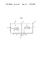
- FIG. 1 is a schematic representation of an electrochemical cell which incorporates a photoanode and a counter electrode in accordance with the invention
- FIG. 2 is a plot of current density vs. electrode potential for amorphous TiO 2 reactively sputtered at three different oxygen partial pressures: (a) 1% O 2 /Ar, (b) 2.5% O 2 /Ar, and (c) 5% O 2 /Ar, illustrating the effect of different degrees of amorphocity on photoresponse;
- FIG. 3 is a plot of photocurrent vs. electrode potential (vs. S.C.E.) for cathodically treated amorphous TiO 2 films annealed for 30 minutes at (a) room temperature, (b) 120° C., (c) 210° C., (d) 300° C., (e) 400° C., and (f) single crystal, illustrating the effect of hydrogenation at different annealing temperatures;
- FIG. 4 is a plot of current density vs. electrode potential (vs. S.C.E.) for hydrogenated amorphous TiO 2 films illustrating the effect of a second compensating agent, aluminum;
- FIG. 5 is a plot of photocurrent vs. time (hours) for two hydrogenated amorphous TiO 2 films illustrating the stability imparted by annealing prior to cathodic treatment in accordance with the present invention
- FIG. 6 is a plot of the quantum efficiency (%) vs. wavelength for hydrogenated amorphous TiO 2 films modified with (a) aluminum and silicon, (b) aluminum and (c) silicon illustrating the increase in quantum efficiencies due to modification with a second modifying agent and a second compensating agent in comparison to (d) single crystal TiO 2 ;
- FIG. 7 is a plot of the photospectral response vs. wavelength for amorphous TiO 2 film co-sputtered with silicon and two amorphous TiO 2 films chemically modified with iron or praseodymium illustrating the increase in photoresponse due to modification with a second modifying agent.
- the cell 10 includes a container 12 with a photoanode 14 and a counter electrode 16 immersed in an electrolyte. The two electrodes are separated by a membrane 18.
- the photoanode has a substrate 20 with a deposition surface 22.
- the substrate 20 can be stainless steel or any other material which provides a conductive support.
- titanium or stainless steel tin oxide coated glass (NESA glass) is utilized as the substrate material.
- the photoelectrochemical device 10 illustrated has a photoanode 14 constructed in a manner described below.
- a suitable electrolyte 30 is then placed in the container 12 to cover the photoanode 14 and counter electrode 16.
- Light 32 is allowed to enter the cell 10 from the top of the container 12 to illuminate the photoanode and photoelectrolysis will occur according to the above described reactions.
- a photoanode has been utilized above described cell for the conversion of light into electrical energy.
- the operation can be assisted by replacing the load 28 with a source of electrical power.
- deposition techniques such as sputter or evaporation deposition and plasma or glow discharge deposition can be utilized to deposit an amorphous semiconductor layer on the substrate deposition surface 22. These techniques allow for selectively incorporating a modifier in the host matrix of the semiconductor material by deposition. Thus, amorphous semiconductor materials are tailor-made in accordance with the present invention to improve their photoresponse and other advantages cited herein.
- n-type amorphous semiconductor is preferably titanium dioxide.
- Other n-type amorphous semiconductor materials contemplated by the present invention include, but are not limited to, the oxides, selenides, sulfides, and phosphides of the transition elements. More particularly, Fe 2 O 3 , SrTiO 3 , WO 3 , and n-doped Si:F:H alloys are contemplated.
- the sputtering power may be in the range of 1/2 watt/cm 2 to 2 watts/cm 2 and preferably 1 watt/cm 2 , as excessive power will tend to form an undesirable substantially polycrystalline film.
- the temperature of the substrate during co-sputtering usually was held in the range of approximately 20° C. to 80° C.
- the stoichiometry of the preferred amorphous semiconductor films prepared by reactive co-sputtering, in accordance with the present invention, can easily be controlled by changing the partial pressure of the oxygen atmosphere, sputtering power and deposition of substrate temperature.
- the degree of disorder of the preferred amorphous semiconductor films can be controlled by varying the oxygen partial pressure, deposition temperature, and the sputtering power.
- the photoresponse of amorphous semiconductor films may be significantly enhanced by modification with a compensating agent incorporated in the semiconductor film.
- the compensating agent compensates or eliminates the localized states in the band gap of the material which would otherwise have a detrimental effect upon the photoresponse of the semiconductor material.
- the present invention contemplates the use of any agent which effectively compensates for the localized states in the band gap of the material, the following materials are particularly useful for accomplishing these means: hydrogen, lithium, fluorine, beryllium, aluminum, boron, magnesium, other Group I elements, and compounds made with these elements.
- the compensating agent is present in an amount of about one atomic percent.
- One of the preferred methods of modifying an amorphous semiconductor with a compensating agent is through electrochemical compensation.
- cathodic treatment is accomplished by placing the semiconductor film in an electrolyte and applying an electrical bias for several minutes.
- the preferred electrolyte is sodium hydroxide with a concentration of about 0.1M.
- Other suitable electrolytes are, for example, lithium hydroxide and potassium hydroxide.
- An appropriate electrical bias is between -1.2 to 2.0 volts applied for not more than about 10 minutes.
- hydrogenation is used to modify the semiconductor film during cathodic treatment.
- a second preferred method of modifying the amorphous semiconductor with a compensating agent is by co-sputtering. During the formation of the semiconductor film, a compensating agent is simultaneously sputtered with the semiconductor material to codeposit a film. Subsequently, the compensated amorphous semiconductor film is subjected to the cathodic treatment described above.
- amorphous semiconductor materials can be used as photoanodes and effective photocatalysts to convert light into electrical energy depends on their band gap and flat-band potentials in the electrolyte. Materials of small band gap and more negative flat-band potential are suitable for use as photoanodes.
- the amount of charge associated with the enhancement of the photocurrent was measured on an electrode made with an amorphous titanium dioxide film in accordance with the present invention. First the voltage of this electrode was taken to a negative value in the dark for hydrogenation (approximately 3 minutes at about -1.6 volts with respect to S.C.E.). Secondly the electrode was taken to an anodic potential (+0.3 volts) before water oxidation in the dark takes place. Then the photocurrent was measured.
- the present invention improves the stability of the materials disclosed herein by heating the semiconductor films prior to cathodic treatment.
- the heat treatment or annealing takes place in an inert atmosphere, preferably argon or nitrogen.
- a suitable temperature range is about 200° C. to 400° C. for about 30 minutes.
- the preferred temperature range is about 200° C. to 250° C.
- the width of the band gap and the stability of the photoelectrode used in water electrolysis is correlated; the smaller the band gap, the more unstable the photoelectrode is; the larger the band gap, the more stable it is.
- Small band gap materials however, are usually more photoresponsive to visible light than larger band gap materials.
- modified semiconductor materials of the present invention have large band gaps. Because of their stability in photoelectrolysis application, these modified semiconductor materials may be utilized as a protective window coating over small band gap materials to make a tandem photoanode. Such a coating may be sufficiently thick to protect the small band gap material from corrosion, yet leave the overall quantum efficiency of the tandem photoanode unaffected.
- One of the methods of making a tandem photoanode using modified semiconductor materials of the present invention is by sputtering or co-sputtering the large band gap material on the small band gap material.
- the tandem photoanode is then subjected to the cathodic treatment discussed above.
- amorphous titanium dioxide is used as the modified semiconductor material having the large band gap.
- the conversion efficiencies are as good as the best results achieved with single crystal TiO 2 .
- the band gap of these materials can be reduced by a second class of modifying agent incorporated into the amorphous semiconductor.
- the second class of modifying agents includes silicon, transition elements, lanthanides, and compounds of these elements.
- the preferred elements are silicon, chromium, iron, niobium, and praseodymium.
- the preferred amount incorporated in the amorphous semiconductor is not more than about 20 atom percent.
- Titanium targets were used to reactively sputter three titanium substrates using different oxygen partial pressures i.e 1%, 2.5%, 5% O 2 /Ar at a constant sputtering power and different substrate temperatures.
- a reactive sputtering atmosphere containing approximately 2.5% oxygen in argon and a substrate temperature of 20° C. to 80° C. provided the most photoresponsive material.
- Increasing the oxygen partial pressure clearly increased the degree of crystallinity in the film as shown by X-ray diffraction studies.
- FIGS. 2a-2c These films were subsequently hydrogenated for 90 minutes.
- the following bias potentials were used: (a) -1.5 v; (b) -2.0 v; (c) -1.2 v.
- the photocurrent of the resulting film dramatically increased in comparison to the untreated films as illustrated in FIGS. 2a-2c.
- FIG. 2a illustrates a substantial increase in photocurrent for the most amorphous film due to hydrogenation.
- the most crystalline film (FIG. 2c) showed a smaller increase in photocurrent.
- the photocurrent for the most amorphous electrode after hydrogenation was higher than the film annealed at 400° C. also treated with the hydrogenation process (compare FIG. 3 a vs. e).
- the photocurrent of the modified electrode is quite stable. During anodic polarization in the light, or in the dark, the photocurrent decreases very slowly. Leaving the cell at open circuit potential or in air for a period of two weeks, the photocurrent decreased by a factor of 3 to 5, but upon short cathodic treatment, the photocurrent was restored to the original value.
- the photocurrent with single crystal TiO 2 electrode on the contrary, decreased upon cathodic reduction under the same conditions.
- a photoanode was prepared by reactive co-sputtering from a target composed of 95% titanium and 5% aluminum in a 1% oxygen/argon atmosphere onto a titanium substrate.
- the use of the compensating agent aluminum did not show any appreciable photoresponse when illuminated in 0.1N NaOH electrolyte with xenon lamp adjusted to 100 mw/cm 2 .
- the photoanode was cathodically treated at the potential region where hydrogen evolution takes place, a dramatic improvement in the photoresponse was noticed. This improvement is illustrated in FIG. 4. This dramatic increase was accomplished without annealing the modified film. It should be noted that the quantum efficiency was also double that of a hydrogenated sample without aluminum modification and that the photocurrent was stable for a prolonged period of time.
- Two photoanodes were prepared with amorphous TiO 2 films reactively sputtered on titanium substrates. Subsequently, one of the films was heated to a temperature of 210° C. for 10 minutes in an argon atmosphere. Both films were then hydrogenated. As illustrated in FIG. 5, the photocurrent of the heat treated or annealed film was very stable under continuous illumination for over 40 hours. Even after three months exposed to air, no degradation of the photocurrent was observed.
- a photoanode having a tandem structure was made by depositing an amorphous film of TiO 2 approximately 0.2 ⁇ thick on a pressed pellet of (CdS) 0 .77 (CdSe) 0 .23. The film was then electrochemically hydrogenated at room temperature.
- the stability of the low band semiconductor material was greatly enhanced without reducing the photoresponse of the low band gap material. No deterioration was observed for several hours at the most anodic potentials until pin holes in the very thin film (0.2 ⁇ ) allowed corrosion to slowly decrease the photoelectrochemical response. It is believed that a more uniform coating would result in even greater stability.
- amorphous modified TiO 2 thin film photoanodes were prepared by reactive co-sputtering of titanium in 1% O 2 /Ar atmosphere on a titanium substrate using aluminum as a compensating agent in one sample, silicon as a second modifying element on a second sample and both elements on a third sample. These films did not show the usual improvement in photocurrent consistent with the present invention; even after cathodic treatment of -1.6 v (vs. SCE) for 3 minutes. Both films were then annealed in an argon atmosphere at 960° C. which dramatically improved their photoelectrochemical properties. Subsequently, these films were hydrogenated and a further improvement in photoresponse resulted. The quantum efficiency of these samples for various wavelengths are presented in FIG. 6. The results for a single crystal TiO 2 annealed at 960° C. in a hydrogen atmosphere are also included for a comparison of the dramatic improvement achieved by the present invention.
- Amorphous TiO 2 films reactively R.F. sputtered on a titanium substrate were chemically modified by soaking the photoanodes in either a saturated solution of Fe(C 2 O 4 ) 3 or a solution of Pr(NO 3 ) 3 with nitric acid. After soaking, the photoanodes were annealed in an argon atmosphere at 850° C. for a 1/2 hour. The photospectral response of the two resulting photoanodes in 0.1N. NaOH at 0.0 v (SCE) is found in FIG. 7. Although the shift of the solar energy absorption range into the visible region was not as substantial for these chemically modified materials as for the materials modified by co-sputtering, chemical modification by soaking proves another simple and inexpensive method to improve the photoactivity of photoanodes.
- the present invention contemplates two classes of modifiers.
- One class of modifiers includes hydrogen, lithium, fluorine, aluminum, other Group I elements, and compounds of these elements. These modifiers compensate or eliminate the localized states in the band gap of the amorphous semiconductor.
- the second class of modifiers includes silicon, transition elements, lanthanides, and compounds of these elements. This second class of modifiers have appropriate energy levels in the band gap between conduction and valence band of the semiconductor and are also to shift its solar absorption range into the visible region.
- an advantage of the amorphous materials of the present invention is that they are easier to make in comparison to the strict requirements discussed above for doping crystalline materials. Although localized states in the gap exist, they can be compensated or passivated by modification with a compensating agent.
Abstract
Description
Claims (42)
Priority Applications (7)
| Application Number | Priority Date | Filing Date | Title |
|---|---|---|---|
| US06/499,900 US4511638A (en) | 1983-06-01 | 1983-06-01 | Photoresponsive amorphous semiconductor materials, methods of making the same, and photoanodes made therewith |
| ZA844029A ZA844029B (en) | 1983-06-01 | 1984-05-28 | Improved photoresponsive amorphous semiconductor materials,methods of making the same,and photoanodes made therewith |
| EP84850164A EP0130159A1 (en) | 1983-06-01 | 1984-05-29 | Improved photoresponsive amorphous semiconductor materials, methods of making same, and photoanodes made therewith |
| CA000455356A CA1202107A (en) | 1983-06-01 | 1984-05-29 | Photoanodes made from photoresponsive amorphous semiconductor materials |
| IN375/CAL/84A IN162756B (en) | 1983-06-01 | 1984-05-30 | |
| JP59112189A JPS6012682A (en) | 1983-06-01 | 1984-05-31 | Method of producing light responsive amorphous semiconductormaterial, photoanode produced by same material and photoelectrochemical cell including same photoanode |
| AU28919/84A AU558308B2 (en) | 1983-06-01 | 1984-05-31 | Photoresponive amorphous alloys and photoanodes made therewith |
Applications Claiming Priority (1)
| Application Number | Priority Date | Filing Date | Title |
|---|---|---|---|
| US06/499,900 US4511638A (en) | 1983-06-01 | 1983-06-01 | Photoresponsive amorphous semiconductor materials, methods of making the same, and photoanodes made therewith |
Publications (1)
| Publication Number | Publication Date |
|---|---|
| US4511638A true US4511638A (en) | 1985-04-16 |
Family
ID=23987212
Family Applications (1)
| Application Number | Title | Priority Date | Filing Date |
|---|---|---|---|
| US06/499,900 Expired - Lifetime US4511638A (en) | 1983-06-01 | 1983-06-01 | Photoresponsive amorphous semiconductor materials, methods of making the same, and photoanodes made therewith |
Country Status (7)
| Country | Link |
|---|---|
| US (1) | US4511638A (en) |
| EP (1) | EP0130159A1 (en) |
| JP (1) | JPS6012682A (en) |
| AU (1) | AU558308B2 (en) |
| CA (1) | CA1202107A (en) |
| IN (1) | IN162756B (en) |
| ZA (1) | ZA844029B (en) |
Cited By (21)
| Publication number | Priority date | Publication date | Assignee | Title |
|---|---|---|---|---|
| EP0982780A1 (en) * | 1998-01-23 | 2000-03-01 | NAKATA, Josuke | Solar battery module for optical electrolysis device and optical electrolysis device |
| US6194346B1 (en) * | 1996-08-05 | 2001-02-27 | Nippon Sheet Glass Co., Ltd. | Photocatalyst and method of making |
| EP1125636A1 (en) * | 1998-08-21 | 2001-08-22 | Ecodevice Laboratory Co., Ltd | Visible radiation type photocatalyst and production method thereof |
| GB2385602A (en) * | 2002-02-20 | 2003-08-27 | Itm Power Ltd | Photoelectrolysis |
| US20030228727A1 (en) * | 2002-05-07 | 2003-12-11 | Guerra John Michael | Stress-induced bandgap-shifted semiconductor photoelectrolytic/photocatalytic/photovoltaic surface and method for making same |
| WO2004050961A1 (en) * | 2002-11-27 | 2004-06-17 | University Of Toledo, The | Integrated photoelectrochemical cell and system having a liquid electrolyte |
| US20040262154A1 (en) * | 2003-06-27 | 2004-12-30 | Gibson Thomas L. | Photoelectrochemical device and electrode |
| US20050059186A1 (en) * | 2003-09-15 | 2005-03-17 | Kelly Nelson A. | Photoelectrochemical device and method of making |
| US20050092357A1 (en) * | 2003-10-29 | 2005-05-05 | Xunming Deng | Hybrid window layer for photovoltaic cells |
| US20070034253A1 (en) * | 2005-08-10 | 2007-02-15 | Yoshinori Nakagawa | Manufacturing method for semiconductor photoelectrochemical cell and semiconductor photoelectrochemical cell |
| US20080073205A1 (en) * | 2005-04-11 | 2008-03-27 | University Of Toledo | Integrated photovoltaic-electrolysis cell |
| US20080223439A1 (en) * | 2004-02-19 | 2008-09-18 | Xunming Deng | Interconnected Photoelectrochemical Cell |
| US20080283121A1 (en) * | 2002-05-07 | 2008-11-20 | Nanoptek Corporation | Bandgap-shifted semiconductor surface and method for making same, and apparatus for using same |
| US20080299697A1 (en) * | 2002-05-07 | 2008-12-04 | Nanoptek Corporation | Bandgap-shifted semiconductor surface and method for making same, and apparatus for using same |
| US20090116095A1 (en) * | 2002-05-07 | 2009-05-07 | Guerra John M | Stress-induced bandgap-shifted semiconductor photoelectrolytic/photocatalytic/photovoltaic surface and method for making same |
| US20090183994A1 (en) * | 2005-09-09 | 2009-07-23 | University Of Nevada, Reno | Preparation of nano-tubular titania substrate with oxygen vacancies and their use in photo-electrolysis of water |
| US20110168549A1 (en) * | 2008-06-02 | 2011-07-14 | Roustaei Alex Hr | Optimised supply source and storage unit for cryogenic power or nanohydride assistance using photovoltaics for on-demand energy production systems |
| WO2012083220A2 (en) * | 2010-12-16 | 2012-06-21 | The Regents Of The University Of California | Generation of highly n-type, defect passivated transition metal oxides using plasma fluorine insertion |
| ITMI20102441A1 (en) * | 2010-12-29 | 2012-06-30 | Eni Spa | TANDEM PHOTOELECTROLYTIC CELL FOR PHOTO-OXIDATION OF SULFURS WITH HYDROGEN PRODUCTION |
| US20130337152A1 (en) * | 2012-06-13 | 2013-12-19 | The Regents Of The University Of California | Hydrogen-treated Semiconductor Metal Oxides for Photoelectrical Water Splitting |
| US11186917B2 (en) | 2018-01-30 | 2021-11-30 | The Board Of Trustees Of The University Of Alabama | Composite electrodes and methods for the fabrication and use thereof |
Families Citing this family (1)
| Publication number | Priority date | Publication date | Assignee | Title |
|---|---|---|---|---|
| WO1991016719A2 (en) * | 1990-04-17 | 1991-10-31 | Michael Graetzel | Photovoltaic cells |
Family Cites Families (6)
| Publication number | Priority date | Publication date | Assignee | Title |
|---|---|---|---|---|
| JPS5913831B2 (en) * | 1975-03-17 | 1984-04-02 | 健一 本多 | electrochemical photocell |
| US4226898A (en) * | 1978-03-16 | 1980-10-07 | Energy Conversion Devices, Inc. | Amorphous semiconductors equivalent to crystalline semiconductors produced by a glow discharge process |
| US4239554A (en) * | 1978-07-17 | 1980-12-16 | Shunpei Yamazaki | Semiconductor photoelectric conversion device |
| JPS5648125A (en) * | 1979-09-28 | 1981-05-01 | Asahi Chemical Ind | Silicon board composite structure semiconductor electrode |
| JPS5844748B2 (en) * | 1981-07-02 | 1983-10-05 | 株式会社東芝 | How to split water |
| US4460443A (en) * | 1982-09-09 | 1984-07-17 | The Regents Of The University Of California | Electrolytic photodissociation of chemical compounds by iron oxide electrodes |
-
1983
- 1983-06-01 US US06/499,900 patent/US4511638A/en not_active Expired - Lifetime
-
1984
- 1984-05-28 ZA ZA844029A patent/ZA844029B/en unknown
- 1984-05-29 CA CA000455356A patent/CA1202107A/en not_active Expired
- 1984-05-29 EP EP84850164A patent/EP0130159A1/en not_active Withdrawn
- 1984-05-30 IN IN375/CAL/84A patent/IN162756B/en unknown
- 1984-05-31 JP JP59112189A patent/JPS6012682A/en active Pending
- 1984-05-31 AU AU28919/84A patent/AU558308B2/en not_active Expired - Fee Related
Non-Patent Citations (10)
| Title |
|---|
| J. J. Cuomo et al, IBM Tech. Disc. Bull., vol. 19, p. 2359, (1976). * |
| J. P. Frayret et al, "Electrochimica Acta", vol. 27, pp. 1525-1528, (1982). |
| J. P. Frayret et al, Electrochimica Acta , vol. 27, pp. 1525 1528, (1982). * |
| K. Rajeshwar et al, Electrochimica Acta, vol. 23, p. 1126, (1978). * |
| M. F. Weber et al, J. Electrochem. Soc., vol. 129, pp. 2022 2028, (1982). * |
| M. F. Weber et al, J. Electrochem. Soc., vol. 129, pp. 2022-2028, (1982). |
| P. Clechet et al, J. Electrochem. Soc., vol. 130, pp. 1795 1796, (1983). * |
| P. Clechet et al, J. Electrochem. Soc., vol. 130, pp. 1795-1796, (1983). |
| Y. Matsumoto et al, J. Electrochem. Soc., vol. 128, pp. 1040 1044, (1981). * |
| Y. Matsumoto et al, J. Electrochem. Soc., vol. 128, pp. 1040-1044, (1981). |
Cited By (54)
| Publication number | Priority date | Publication date | Assignee | Title |
|---|---|---|---|---|
| US6194346B1 (en) * | 1996-08-05 | 2001-02-27 | Nippon Sheet Glass Co., Ltd. | Photocatalyst and method of making |
| EP0982780A4 (en) * | 1998-01-23 | 2001-08-16 | Josuke Nakata | Solar battery module for optical electrolysis device and optical electrolysis device |
| EP0982780A1 (en) * | 1998-01-23 | 2000-03-01 | NAKATA, Josuke | Solar battery module for optical electrolysis device and optical electrolysis device |
| US6908881B1 (en) | 1998-08-21 | 2005-06-21 | Ecodevice Laboratory Co., Ltd. | Visible radiation type photocatalyst and production method thereof |
| EP1125636A1 (en) * | 1998-08-21 | 2001-08-22 | Ecodevice Laboratory Co., Ltd | Visible radiation type photocatalyst and production method thereof |
| EP1125636A4 (en) * | 1998-08-21 | 2002-03-06 | Ecodevice Lab Co Ltd | Visible radiation type photocatalyst and production method thereof |
| GB2385602A (en) * | 2002-02-20 | 2003-08-27 | Itm Power Ltd | Photoelectrolysis |
| US20030226762A1 (en) * | 2002-02-20 | 2003-12-11 | Highgate Donald James | Method of photoelectrolysis |
| GB2385602B (en) * | 2002-02-20 | 2004-04-21 | Itm Power Ltd | Method of photoelectrolysis |
| US7318888B2 (en) | 2002-02-20 | 2008-01-15 | Itm Power Ltd | Method of photoelectrolysis |
| US20070017794A1 (en) * | 2002-02-20 | 2007-01-25 | Highgate Donald J | Method of photoelectrolysis |
| US7992528B2 (en) | 2002-05-07 | 2011-08-09 | Nanoptek Corporation | Stress-induced bandgap-shifted semiconductor photoelectrolytic/photocatalytic/photovoltaic surface and method for making same |
| US7947221B2 (en) | 2002-05-07 | 2011-05-24 | Guerra John M | Stress-induced bandgap-shifted semiconductor photoelectrolytic/photocatalytic/photovoltaic surface and method for making same |
| US7628928B2 (en) | 2002-05-07 | 2009-12-08 | Guerra John M | Stress-induced bandgap-shifted semiconductor photoelectrolytic/photocatalytic/photovoltaic surface and method for making same |
| US20090127124A1 (en) * | 2002-05-07 | 2009-05-21 | John Michael Guerra | Stress-induced bandgap-shifted semiconductor photoelectrolytic/photocatalytic/photovoltaic surface and method for making same |
| US20090116095A1 (en) * | 2002-05-07 | 2009-05-07 | Guerra John M | Stress-induced bandgap-shifted semiconductor photoelectrolytic/photocatalytic/photovoltaic surface and method for making same |
| US20090107548A1 (en) * | 2002-05-07 | 2009-04-30 | John Michael Guerra | Stress-induced bandgap-shifted semiconductor photoelectrolytic/photocatalytic/photovoltaic surface and method for making same |
| US9847439B2 (en) | 2002-05-07 | 2017-12-19 | Nanoptek Corporation | Stress-induced bandgap-shifted semiconductor photoelectrolytic/photocatalytic/photovoltaic surface and method for making same |
| US8673399B2 (en) | 2002-05-07 | 2014-03-18 | Nanoptek Corporation | Bandgap-shifted semiconductor surface and method for making same, and apparatus for using same |
| US20090110591A1 (en) * | 2002-05-07 | 2009-04-30 | John Michael Guerra | Stress-induced bandgap-shifted semiconductor photoelectrolytic/photocatalytic/photovoltaic surface and method for making same |
| US7995871B2 (en) | 2002-05-07 | 2011-08-09 | Nanoptek Corporation | Stress-induced bandgap-shifted semiconductor photoelectrolytic/photocatalytic/photovoltaic surface and method for making same |
| US20030228727A1 (en) * | 2002-05-07 | 2003-12-11 | Guerra John Michael | Stress-induced bandgap-shifted semiconductor photoelectrolytic/photocatalytic/photovoltaic surface and method for making same |
| US20100040514A1 (en) * | 2002-05-07 | 2010-02-18 | John Michael Guerra | Stress-induced bandgap-shifted semiconductor photoelectrolytic/photocatalytic/photovoltaic surface and method for making same |
| US20080283121A1 (en) * | 2002-05-07 | 2008-11-20 | Nanoptek Corporation | Bandgap-shifted semiconductor surface and method for making same, and apparatus for using same |
| US20080299697A1 (en) * | 2002-05-07 | 2008-12-04 | Nanoptek Corporation | Bandgap-shifted semiconductor surface and method for making same, and apparatus for using same |
| US7485799B2 (en) * | 2002-05-07 | 2009-02-03 | John Michael Guerra | Stress-induced bandgap-shifted semiconductor photoelectrolytic/photocatalytic/photovoltaic surface and method for making same |
| US20090101420A1 (en) * | 2002-05-07 | 2009-04-23 | John Michael Guerra | Stress-induced bandgap-shifted semiconductor photoelectrolytic/photocatalytic/photovoltaic surface and method for making same |
| WO2004050961A1 (en) * | 2002-11-27 | 2004-06-17 | University Of Toledo, The | Integrated photoelectrochemical cell and system having a liquid electrolyte |
| US20050211290A1 (en) * | 2002-11-27 | 2005-09-29 | The University Of Toledo | Integrated photoelectrochemical cell and system having a liquid electrolyte |
| US7750234B2 (en) | 2002-11-27 | 2010-07-06 | The University Of Toledo | Integrated photoelectrochemical cell and system having a liquid electrolyte |
| US20040262154A1 (en) * | 2003-06-27 | 2004-12-30 | Gibson Thomas L. | Photoelectrochemical device and electrode |
| US7052587B2 (en) | 2003-06-27 | 2006-05-30 | General Motors Corporation | Photoelectrochemical device and electrode |
| US20050059186A1 (en) * | 2003-09-15 | 2005-03-17 | Kelly Nelson A. | Photoelectrochemical device and method of making |
| US8030120B2 (en) | 2003-10-29 | 2011-10-04 | The University Of Toledo | Hybrid window layer for photovoltaic cells |
| US20080000524A1 (en) * | 2003-10-29 | 2008-01-03 | University Of Toledo | Hybrid window layer for photovoltaic cells |
| US7879644B2 (en) | 2003-10-29 | 2011-02-01 | The University Of Toledo | Hybrid window layer for photovoltaic cells |
| US20080166833A1 (en) * | 2003-10-29 | 2008-07-10 | University Of Toledo | Hybrid window layer for photovoltaic cells |
| US20050092357A1 (en) * | 2003-10-29 | 2005-05-05 | Xunming Deng | Hybrid window layer for photovoltaic cells |
| US7667133B2 (en) | 2003-10-29 | 2010-02-23 | The University Of Toledo | Hybrid window layer for photovoltaic cells |
| US20080223439A1 (en) * | 2004-02-19 | 2008-09-18 | Xunming Deng | Interconnected Photoelectrochemical Cell |
| US20080073205A1 (en) * | 2005-04-11 | 2008-03-27 | University Of Toledo | Integrated photovoltaic-electrolysis cell |
| US7927914B2 (en) | 2005-08-10 | 2011-04-19 | Shiken Co., Ltd. | Manufacturing method for semiconductor photoelectrochemical cell and semiconductor photoelectrochemical cell |
| US20070034253A1 (en) * | 2005-08-10 | 2007-02-15 | Yoshinori Nakagawa | Manufacturing method for semiconductor photoelectrochemical cell and semiconductor photoelectrochemical cell |
| US20090183994A1 (en) * | 2005-09-09 | 2009-07-23 | University Of Nevada, Reno | Preparation of nano-tubular titania substrate with oxygen vacancies and their use in photo-electrolysis of water |
| US20110168549A1 (en) * | 2008-06-02 | 2011-07-14 | Roustaei Alex Hr | Optimised supply source and storage unit for cryogenic power or nanohydride assistance using photovoltaics for on-demand energy production systems |
| US9312342B2 (en) | 2010-12-16 | 2016-04-12 | The Regents Of The University Of California | Generation of highly N-type, defect passivated transition metal oxides using plasma fluorine insertion |
| WO2012083220A3 (en) * | 2010-12-16 | 2013-07-11 | The Regents Of The University Of California | Generation of highly n-type, defect passivated transition metal oxides using plasma fluorine insertion |
| WO2012083220A2 (en) * | 2010-12-16 | 2012-06-21 | The Regents Of The University Of California | Generation of highly n-type, defect passivated transition metal oxides using plasma fluorine insertion |
| WO2012089792A3 (en) * | 2010-12-29 | 2012-08-30 | Eni S.P.A. | Tandem photoelectrolytic cell for the photo-oxidation of sulfides with the production of hydrogen |
| ITMI20102441A1 (en) * | 2010-12-29 | 2012-06-30 | Eni Spa | TANDEM PHOTOELECTROLYTIC CELL FOR PHOTO-OXIDATION OF SULFURS WITH HYDROGEN PRODUCTION |
| US20130337152A1 (en) * | 2012-06-13 | 2013-12-19 | The Regents Of The University Of California | Hydrogen-treated Semiconductor Metal Oxides for Photoelectrical Water Splitting |
| US9379422B2 (en) * | 2012-06-13 | 2016-06-28 | The Regents Of The University Of California | Hydrogen-treated semiconductor metal oxides for photoelectrical water splitting |
| US11186917B2 (en) | 2018-01-30 | 2021-11-30 | The Board Of Trustees Of The University Of Alabama | Composite electrodes and methods for the fabrication and use thereof |
| US11959182B2 (en) | 2018-01-30 | 2024-04-16 | The Board Of Trustees Of The University Of Alabama | Composite electrodes and methods for the fabrication and use thereof |
Also Published As
| Publication number | Publication date |
|---|---|
| CA1202107A (en) | 1986-03-18 |
| EP0130159A1 (en) | 1985-01-02 |
| ZA844029B (en) | 1985-01-30 |
| AU2891984A (en) | 1985-07-04 |
| JPS6012682A (en) | 1985-01-23 |
| IN162756B (en) | 1988-07-09 |
| AU558308B2 (en) | 1987-01-22 |
Similar Documents
| Publication | Publication Date | Title |
|---|---|---|
| US4511638A (en) | Photoresponsive amorphous semiconductor materials, methods of making the same, and photoanodes made therewith | |
| Wrighton et al. | Photoelectrolysis of water by irradiation of platinized n-type semiconducting metal oxides | |
| Bak et al. | Photo-electrochemical properties of the TiO2-Pt system in aqueous solutions | |
| Natarajan et al. | Cathodic electrodeposition of nanocrystalline titanium dioxide thin films | |
| Marsen et al. | Progress in sputtered tungsten trioxide for photoelectrode applications | |
| US4521499A (en) | Highly conductive photoelectrochemical electrodes and uses thereof | |
| US4656103A (en) | Liquid junction photoelectrodes using amorphous silicon-based thin film semiconductor | |
| US4436558A (en) | Electrochemical photovoltaic cell having ternary alloy film | |
| Millenbach et al. | The electrochemical formation of titanium hydride | |
| Wagner et al. | Photocatalytic hydrogen production from water over SrTiO3 crystal surfaces, electron spectroscopy studies of adsorbed H2, O2 and H2O | |
| HU199575B (en) | Electrodes applicable by electrolise and process for their production | |
| Takahashi et al. | Electrochemical deposition, optical properties, and photoelectrochemical behavior of CdTe films | |
| Paulauskas et al. | Photoelectrochemical stability and alteration products of n-type single-crystal ZnO photoanodes | |
| CA1237510A (en) | Liquid junction photoelectrodes using amorphous silicon-based thin film semiconductor | |
| Minoura et al. | CdS-electrochemical photocell with S2− ion-containing electrolyte | |
| Dalard et al. | Electrochemical incorporation of lithium into palladium from aprotic electrolytes | |
| Schumacher et al. | Novel, Colloidally Rough, In2 O 3 Films Displaying High Quantum Efficiencies | |
| US10683577B1 (en) | Method of producing hydrogen peroxide using nanostructured bismuth oxide | |
| US20070235711A1 (en) | Methods of reducing the bandgap energy of a metal oxide | |
| Gutierrez et al. | New semiconducting oxide photoanodes for water splitting in a photoelectrochemical cell Electrochemistry of n-type NiTiO3 | |
| Prasad et al. | Structural and photoelectrochemical studies of In2O3-TiO2 and WSe2 photoelectrodes for photoelectrochemical production of hydrogen | |
| US4396485A (en) | Film photoelectrodes | |
| SU786921A3 (en) | Method of making electrode for electrochemical processes | |
| US4154662A (en) | Process and apparatus for the electrolytic production of hydrogen | |
| EP0036709B1 (en) | Process for manufacturing a polychelate coating and electrode coated therewith |
Legal Events
| Date | Code | Title | Description |
|---|---|---|---|
| AS | Assignment |
Owner name: ENERGY CONVERSION DEVICES, INC., 1675 WEST MAPLE R Free format text: ASSIGNMENT OF ASSIGNORS INTEREST.;ASSIGNORS:SAPRU, KRISHNA;REICHMAN, BENJAMIN;LIANG, GAO;REEL/FRAME:004139/0675 Effective date: 19830526 |
|
| STCF | Information on status: patent grant |
Free format text: PATENTED CASE |
|
| CC | Certificate of correction | ||
| AS | Assignment |
Owner name: NATIONAL BANK OF DETROIT, 611 WOODWARD AVENUE, DET Free format text: SECURITY INTEREST;ASSIGNOR:ENERGY CONVERSION DEVICES, INC., A DE. CORP.;REEL/FRAME:004661/0410 Effective date: 19861017 Owner name: NATIONAL BANK OF DETROIT, MICHIGAN Free format text: SECURITY INTEREST;ASSIGNOR:ENERGY CONVERSION DEVICES, INC., A DE. CORP.;REEL/FRAME:004661/0410 Effective date: 19861017 |
|
| FPAY | Fee payment |
Year of fee payment: 4 |
|
| REMI | Maintenance fee reminder mailed | ||
| FEPP | Fee payment procedure |
Free format text: PAYER NUMBER DE-ASSIGNED (ORIGINAL EVENT CODE: RMPN); ENTITY STATUS OF PATENT OWNER: LARGE ENTITY |
|
| FPAY | Fee payment |
Year of fee payment: 8 |
|
| SULP | Surcharge for late payment | ||
| FPAY | Fee payment |
Year of fee payment: 12 |
|
| AS | Assignment |
Owner name: XYLON LLC, NEVADA Free format text: MERGER;ASSIGNOR:XTREMA LLC;REEL/FRAME:037066/0834 Effective date: 20150813 |