US4527233A - Addressable buffer circuit with address incrementer independently clocked by host computer and external storage device controller - Google Patents
Addressable buffer circuit with address incrementer independently clocked by host computer and external storage device controller Download PDFInfo
- Publication number
- US4527233A US4527233A US06/401,700 US40170082A US4527233A US 4527233 A US4527233 A US 4527233A US 40170082 A US40170082 A US 40170082A US 4527233 A US4527233 A US 4527233A
- Authority
- US
- United States
- Prior art keywords
- data
- controller
- memory
- host computer
- buffer
- Prior art date
- Legal status (The legal status is an assumption and is not a legal conclusion. Google has not performed a legal analysis and makes no representation as to the accuracy of the status listed.)
- Expired - Lifetime
Links
Images
Classifications
-
- G—PHYSICS
- G06—COMPUTING; CALCULATING OR COUNTING
- G06F—ELECTRIC DIGITAL DATA PROCESSING
- G06F5/00—Methods or arrangements for data conversion without changing the order or content of the data handled
- G06F5/06—Methods or arrangements for data conversion without changing the order or content of the data handled for changing the speed of data flow, i.e. speed regularising or timing, e.g. delay lines, FIFO buffers; over- or underrun control therefor
- G06F5/10—Methods or arrangements for data conversion without changing the order or content of the data handled for changing the speed of data flow, i.e. speed regularising or timing, e.g. delay lines, FIFO buffers; over- or underrun control therefor having a sequence of storage locations each being individually accessible for both enqueue and dequeue operations, e.g. using random access memory
Definitions
- This invention relates to data processing systems which employ a host computer or central processing unit and an external data source such as a disk drive or tape unit to provide data to the central processing unit. More particularly, this invention relates to data processing systems which include a peripheral controller for controlling the operation of the external data source, including transfer of data to the central processing unit.
- peripheral controllers to perform various standard functions in order to off-load input/ouput processing from the central processing unit ("CPU") to free it for performing more complex operations.
- CPU central processing unit
- disk controllers which mate a CPU with a magnetic disk drive data storage unit.
- Recent controller systems have included a buffer random access memory (RAM) connected to a controller in order to efficiently receive and store data from the CPU for subsequent transmission to the disk drive or vice versa.
- RAM buffer random access memory
- these prior art systems require that the CPU transmit data to and receive data from the RAM at a rate limited by the processing speed of the controller.
- the present invention eliminates that limitation, permitting the CPU to transmit data to and receive data from the RAM at the CPU's maximum data transfer rate.
- the present invention provides a data processing system which includes a buffer which is directly coupled to both a CPU and to a peripheral controller.
- a DMA controller can be added if desired to enhance CPU-to-buffer data transfer performance). This configuration enables data transfer to be directly controlled by either the peripheral controller or the CPU. By giving the CPU direct control over the buffer, data can be transferred into the buffer at the CPU's data rate.
- the buffer system may consist of a random access memory having a data bus connected to both the CPU and the peripheral controller, and a counter which is used to control the addressing of the random access memory.
- the clocking of the counter is controlled by signals from either the CPU or the peripheral controller.
- a first-in/first-out memory is utilized instead of a counter and RAM.
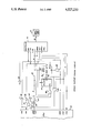
- FIGURE is a partial schematic, partial block diagram of the data processing system of the invention.
- a CPU or host computer 10 may be used to perform various computing functions.
- Data which is utilized by the CPU is stored on an external data storage device 12, which generally is either a disk drive or tape system.
- the external data storage device 12 is a disk drive unit.
- a peripheral controller 14 (which, for example, may be a Western Digital model 1010 controller chip) receives control signals from the CPU 10 to control the operation of the disk drive unit 12.
- the controller 14 controls the disk drive system in order to access appropriate data on the disk, and also controls the actual data transfer to and from the disk. Controllers of this type are well-known in the art and need not be described in detail.
- Data which is stored on a disk is typically divided into a number of sectors, with each sector containing a number of bytes (for example, 128 bytes).
- the buffer RAM 16 of the presently described embodiment is designed to hold one sector's worth of data.
- a buffer RAM 16 is connected via an eight-bit wide data bus 18 to the CPU 10 and to the controller 14.
- Tristate buffers 20 and 22 are located on the data bus 18 to regulate the bi-directional flow of data signals to and from the CPU 10.
- Data flow between the RAM 16 and the CPU 10 and the controller 14 is regulated by means of control signals from both the CPU 10 and controller 14 in conjunction with a counter 24. Depending upon the state of various control signals, data may be transferred between the CPU and disk drive unit, between the CPU and the RAM, or between the controller and the RAM.
- the CPU 10 provides a host buffer chip select control signal HBCS and a host controller chip select control signal HCCS.
- the rate of data transfer to and from the CPU 10 is controlled by a host read enable signal HRE and a host write enable signal HWE.
- the host read enable signal HRE and the host write enable signal HWE are pulsed signals, whose repetition rate is equal to the rate at which the CPU can transmit or receive data over the data bus 18.
- the controller 14 similarly provides a pulsed controller read enable signal CRE and controller write enable signal CWE which regulate the data transfer rate when data is to be transferred between the disk drive and the buffer RAM.
- the repetition rate of the CRE and CWE signals is equal to the rate at which the controller 14 can transmit or receive data over the data bus 18.
- the data transfer rate of the controller is typically less than the data transfer rate of the CPU.
- control signals may be present between the CPU 10 and the controller 14, as is known in the art.
- a host controller chip select signal HCCS is used by the CPU 10 to enable the controller 14 for purposes of transferring control and data information to the controller 14 over the data bus 18 in a manner well known in the art.
- the counter 24 is an eight-bit counter, and in its initialized state its output is a binary zero.
- the first seven bits of the output of the counter are coupled along an address bus 36 to the address input of the RAM 16.
- the counter 24 output causes the corresponding memory location of the RAM 16 to be addressed.
- the buffer RAM 16 has a read enable input coupled to both the host read enable signal HRE and the controller read enable signal CRE.
- the buffer RAM 16 also has a write enable input coupled to both the host write enable signal HWE and the controller write enable signal CWE.
- the counter 24 may be incremented by one binary count by the receipt, through an OR gate 38, of a read enable or a write enable pulse from either the CPU 10 or the controller 14.
- the counter 24 is incremented by the rising edge of a clock signal from the OR gate 38.
- As the counter 24 is incremented a successive memory location in the RAM 16 is addressed for reading or writing at the next clock cycle.
- the incrementing process continues with each clock pulse until the counter state is binary "01111111", which causes the one hundred twenty-eighth byte location in the RAM 16 to be addressed (since the zero byte location is also addressable).
- the state of the counter will be binary "10000000”.
- the most significant bit of the counter 24 is output as a buffer ready signal BRDY to the controller 14.
- the BRDY signal indicates that the counter 24 has cycled through its counting range, thus indicating that the buffer RAM 16 is either empty or full of data.
- the CPU 10 In order to write data from the CPU 10 into the buffer RAM 16, the CPU 10 enables the buffer RAM 16 by activating the host buffer chip select signal HBCS.
- the HBCS signal is connected to one input of an OR gate 26, whose output is connected to the chip select input of the buffer RAM 16.
- the HBCS signal also is connected to an input of an OR gate 28.
- the output of OR gate 28 serves as an enabling signal to two AND gates 33, 34, which are coupled to tristate buffers 20 and 22 on the data bus 18.
- the host read enable signal HRE is coupled as the second input to AND gate 33, and when activated causes tristate buffer 22 to conduct data signals to the CPU over the data bus 18.
- the host write enable signal HWE is coupled as the second input to AND gate 34, and when activated causes tristate buffer 20 to conduct data signals from the CPU over the data bus 18.
- Tristate buffers 30, 32 are provided for the HRE and HWE signal lines, and are controlled by the controller buffer chip select signal CBCS (inverted by inverter 35). The tristate buffers 30, 32 conduct whenever the controller buffer chip select signal CBCS is inactive.
- the CPU 10 In addition to providing the host buffer chip select signal HBCS, the CPU 10 also provides a disk write command by sending appropriate data information and a disk write command code to the controller 14.
- the controller 14 responds to a disk write command by generating a buffer counter reset signal BCR to reset the counter 24 to binary zero.
- the controller 14 then transmits a data request signal DRQ to the CPU 10 which indicates that the CPU can begin writing data into the buffer RAM 16.
- Writing is then controlled by pulsing the write enable signal HWE from the CPU 10 once for each byte of data to be transferred from the CPU 10 to the buffer RAM 16.
- the active HBCS signal is not steady, but is pulsed at the same rate as the HWE or HRE signals.
- the present invention may be used with either CPU architecture.
- the counter 24 When the counter 24 has cycled through its counting range, thus indicating that the CPU 10 has written a sector's worth of a data into the buffer RAM 16, the counter generates the buffer ready signal BRDY, which indicates to the controller 14 that the buffer RAM is full and that data should be transferred from the buffer RAM to the disk drive 12.
- the data request signal DRQ is reset by the controller 14 to indicate to the CPU 10 that the buffer RAM 16 is full.
- the CPU 10 ceases transmitting data to the buffer RAM 16 while the data request signal DRQ is reset, and the host buffer chip select signal HBCS is deactivated.
- the buffer counter reset signal BCR is then generated by the controller 14 to reset the counter 24.
- the controller generates a controller buffer chip select signal CBCS which enables the buffer RAM 16 through OR gate 26.
- Data is read by the controller 14 from the buffer RAM 16 by pulsing the controller read enable signal CRE once for each byte of data to be transferred to the disk drive 12.
- the data is transmitted to the disk drive 12 at the rate of the pulsed read enable signals CRE from the controller 14.
- the counter 24 After all of the data from the buffer RAM 16 has been transferred to the disk drive 12, the counter 24 generates another buffer ready signal BRDY to the controller 14.
- the controller then sets the data request line DRQ to indicate to the CPU 10 that additional information can be written into the buffer RAM 16, and the CPU repeats the write cycle.
- the CPU 10 places the controller 14 into a "read" mode by sending appropriate data identification information and a disk read command code to the controller 14 (with the aid of address control lines not shown, but in a manner known in the art).
- the host buffer chip select signal HBCS is deactivated by the CPU 10, thus deactivating the tristate buffers 20, 22 on the data bus 18.
- the controller 14 then generates a controller buffer chip select signal CBCS which enables the buffer RAM 16 through OR gate 26.
- the controller 14 also generates a buffer counter reset signal BCR to reset counter 24 to binary zero.
- Data is then transferred from the disk drive 12 to the RAM 16 by providing pulsed controller write enable signals CWE from the controller 14 to clock the counter 24, which addresses the RAM 16.
- the buffer ready signal BRDY is transmitted from the counter 24 to the controller 14, indicating that the RAM 16 is full and data can be transferred from it to the CPU 10.
- the controller 14 After the receipt of the buffer ready signal BRDY indicating that the buffer 16 is full, the controller 14 generates a buffer counter reset signal BCR to reset counter 24 to binary zero, sets the data request signal DRQ, and deactivates the controller buffer chip select signal CBCS.
- the DRQ signal allows the CPU 10 to retrieve data from the buffer RAM 16.
- the CPU 10 Upon the setting of DRQ, the CPU 10 activates the host buffer chip select signal HBCS and reads data from the buffer RAM 16 by pulsing the host read enable signal HRE.
- the buffer ready signal BRDY is transmitted to the controller 14, which resets the data request signal DRQ.
- the reset DRQ signal prevents the CPU 10 from attempting further access to the buffer RAM 16.
- the controller 14 will continue to retrieve further data from the disk drive 12 for transfer to the buffer RAM 16 so long as the CPU 10 commands that operation.
- both the CPU unit 10 and the controller 14 have direct access to the buffer RAM 16.
- the CPU 10 can transfer data into the buffer RAM at a rate controlled by the CPU.
- the disk drive 12 and controller 14 can operate at a rate which is different from the CPU 10, thus increasing the efficiency of the CPU with respect to disk input/output operations.
- the buffer circuitry could be incorporated on the same chip as the controller 14.
- a first-in/first-out memory device such as the Western Digital model WD 1510 LIFO/FIFO Buffer Register
- Various other modifications to the invention will be apparent to those skilled in the art.
Abstract
Description
Claims (6)
Priority Applications (1)
| Application Number | Priority Date | Filing Date | Title |
|---|---|---|---|
| US06/401,700 US4527233A (en) | 1982-07-26 | 1982-07-26 | Addressable buffer circuit with address incrementer independently clocked by host computer and external storage device controller |
Applications Claiming Priority (1)
| Application Number | Priority Date | Filing Date | Title |
|---|---|---|---|
| US06/401,700 US4527233A (en) | 1982-07-26 | 1982-07-26 | Addressable buffer circuit with address incrementer independently clocked by host computer and external storage device controller |
Publications (1)
| Publication Number | Publication Date |
|---|---|
| US4527233A true US4527233A (en) | 1985-07-02 |
Family
ID=23588847
Family Applications (1)
| Application Number | Title | Priority Date | Filing Date |
|---|---|---|---|
| US06/401,700 Expired - Lifetime US4527233A (en) | 1982-07-26 | 1982-07-26 | Addressable buffer circuit with address incrementer independently clocked by host computer and external storage device controller |
Country Status (1)
| Country | Link |
|---|---|
| US (1) | US4527233A (en) |
Cited By (41)
| Publication number | Priority date | Publication date | Assignee | Title |
|---|---|---|---|---|
| US4604682A (en) * | 1982-09-30 | 1986-08-05 | Teleplex Corporation | Buffer system for interfacing an intermittently accessing data processor to an independently clocked communications system |
| US4642791A (en) * | 1983-09-15 | 1987-02-10 | Pitney Bowes Inc. | Interface for mailing system peripheral devices |
| US4649474A (en) * | 1983-09-23 | 1987-03-10 | Western Digital Corporation | Chip topography for a MOS disk memory controller circuit |
| US4742454A (en) * | 1983-08-30 | 1988-05-03 | Amdahl Corporation | Apparatus for buffer control bypass |
| FR2607648A1 (en) * | 1986-11-28 | 1988-06-03 | Hewlett Packard France Sa | METHOD AND DEVICE FOR FAST TRANSMISSION OF DATA BETWEEN A TRANSMITTER AND A RECEIVER BY STANDARD SERIAL LINK |
| US4847812A (en) * | 1986-09-18 | 1989-07-11 | Advanced Micro Devices | FIFO memory device including circuit for generating flag signals |
| US4862350A (en) * | 1984-08-03 | 1989-08-29 | International Business Machines Corp. | Architecture for a distributive microprocessing system |
| US4995005A (en) * | 1986-09-18 | 1991-02-19 | Advanced Micro Devices, Inc. | Memory device which can function as two separate memories or a single memory |
| US5003463A (en) * | 1988-06-30 | 1991-03-26 | Wang Laboratories, Inc. | Interface controller with first and second buffer storage area for receiving and transmitting data between I/O bus and high speed system bus |
| US5023829A (en) * | 1987-09-11 | 1991-06-11 | Hitachi, Ltd. | Data transfer system having a channel adapter with varying data transfer lengths |
| US5065354A (en) * | 1988-09-16 | 1991-11-12 | Compaq Computer Corporation | Queued posted-write disk write method with improved error handling |
| US5261057A (en) * | 1988-06-30 | 1993-11-09 | Wang Laboratories, Inc. | I/O bus to system interface |
| WO1994004960A1 (en) * | 1992-08-12 | 1994-03-03 | Digital Theater Systems, L.P. | Motion picture digital sound system and method with primary sound storage edit capability |
| US5345561A (en) * | 1989-01-12 | 1994-09-06 | Nec Corporation | Disk drive control system using a disk controller |
| US5367649A (en) * | 1988-05-20 | 1994-11-22 | Waferscale Integration, Inc. | Programmable controller |
| US5410652A (en) * | 1990-09-28 | 1995-04-25 | Texas Instruments, Incorporated | Data communication control by arbitrating for a data transfer control token with facilities for halting a data transfer by maintaining possession of the token |
| US5412611A (en) * | 1992-03-17 | 1995-05-02 | Fujitsu, Limited | FIFO memory device capable of writing contiguous data into rows |
| US5434979A (en) * | 1987-02-27 | 1995-07-18 | Unisys Corporation | Disk drive controller |
| US5444860A (en) * | 1992-02-14 | 1995-08-22 | Unisys Corporation | Translator system for message transfers between digital units operating on different message protocols and different clock rates |
| US5450146A (en) * | 1989-05-24 | 1995-09-12 | Digital Theater Systems, L.P. | High fidelity reproduction device for cinema sound |
| US5551054A (en) * | 1991-11-19 | 1996-08-27 | Adaptec, Inc. | Page mode buffer controller for transferring Nb byte pages between a host and buffer memory without interruption except for refresh |
| US5604866A (en) * | 1993-09-30 | 1997-02-18 | Silicon Graphics, Inc. | Flow control system having a counter in transmitter for decrementing and incrementing based upon transmitting and received message size respectively for indicating free space in receiver |
| US5640599A (en) * | 1991-12-30 | 1997-06-17 | Apple Computer, Inc. | Interconnect system initiating data transfer over launch bus at source's clock speed and transfering data over data path at receiver's clock speed |
| US5655091A (en) * | 1992-01-30 | 1997-08-05 | Apple Computer, Inc. | Computer system for transferring information streams in a plurality of formats without control information regarding the information streams |
| US5685012A (en) * | 1993-11-09 | 1997-11-04 | Micron Electronics, Inc. | System for employing high speed data transfer between host and peripheral via host interface circuitry utilizing an IOread signal driven by the peripheral or the host |
| US5694545A (en) * | 1991-12-30 | 1997-12-02 | Apple Computer, Inc. | System for providing control of data transmission by destination node using stream values transmitted from plural source nodes |
| WO1998012623A1 (en) * | 1996-09-20 | 1998-03-26 | Honeywell Inc. | Single port first-in-first-out (fifo) storage device having over-write protection and diagnostic capabilities |
| US5745793A (en) * | 1995-06-07 | 1998-04-28 | Seagate Technology, Inc. | Apparatus having a circular buffer that maintains a one entry gap between elements written to the microprocessor and elements operated on by the clock |
| US5751398A (en) * | 1990-09-28 | 1998-05-12 | Digital Theater System, Inc. | Motion picture digital sound system and method |
| US5760607A (en) * | 1995-07-10 | 1998-06-02 | Xilinx, Inc. | System comprising field programmable gate array and intelligent memory |
| US5794056A (en) * | 1993-10-04 | 1998-08-11 | International Business Machines Corporation | System for automatic buffering of commands for DASD units |
| US5848297A (en) * | 1991-12-30 | 1998-12-08 | Apple Computer, Inc. | Control apparatus for maintaining order and accomplishing priority promotion in a computer interconnect |
| US5850574A (en) * | 1996-05-08 | 1998-12-15 | Matsushita Electric Industrial Co., Ltd. | Apparatus for voice encoding/decoding utilizing a control to minimize a time required upon encoding/decoding each subframe of data on the basis of word transfer information |
| US5887196A (en) * | 1991-12-30 | 1999-03-23 | Apple Computer, Inc. | System for receiving a control signal from a device for selecting its associated clock signal for controlling the transferring of information via a buffer |
| US5890012A (en) * | 1995-04-25 | 1999-03-30 | Intel Corporation | System for programming peripheral with address and direction information and sending the information through data bus or control line when DMA controller asserts data knowledge line |
| US5915092A (en) * | 1994-03-25 | 1999-06-22 | Fujitsu Limited | Communications control system for transferring commands/status data in batch between processors utilizing transmitting processor's command activation order and receiving processor's access control |
| US5954807A (en) * | 1995-04-11 | 1999-09-21 | Elonex I.P. Holdings, Ltd. | System for selecting and compressing data and sending temporarily stored compressed data on demand to individual ones of peripheral device selected and gated by interrupt signals |
| WO2000038045A1 (en) * | 1998-12-21 | 2000-06-29 | Koninklijke Philips Electronics N.V. | Fifo unit with single pointer |
| US6128672A (en) * | 1998-03-10 | 2000-10-03 | Motorola, Inc. | Data transfer using software interrupt service routine between host processor and external device with queue of host processor and hardware queue pointers on external device |
| US6219729B1 (en) * | 1998-03-31 | 2001-04-17 | Texas Instruments Incorporated | Apparatus and method for providing for efficient communication between high and low-level processing engine of a disk drive formatter |
| US20030108194A1 (en) * | 2001-12-07 | 2003-06-12 | International Business Machines Corporation | Sequence-preserving multiprocessing system with multimode TDM buffer |
Citations (7)
| Publication number | Priority date | Publication date | Assignee | Title |
|---|---|---|---|---|
| US3587058A (en) * | 1969-06-04 | 1971-06-22 | Bell Telephone Labor Inc | Data processing system input-output arrangement |
| US4122520A (en) * | 1977-05-23 | 1978-10-24 | General Electric Company | Microcomputer controller and direct memory access apparatus therefor |
| US4240138A (en) * | 1978-10-03 | 1980-12-16 | Texas Instruments Incorporated | System for direct access to a memory associated with a microprocessor |
| US4371932A (en) * | 1979-07-30 | 1983-02-01 | International Business Machines Corp. | I/O Controller for transferring data between a host processor and multiple I/O units |
| US4399503A (en) * | 1978-06-30 | 1983-08-16 | Bunker Ramo Corporation | Dynamic disk buffer control unit |
| US4454595A (en) * | 1981-12-23 | 1984-06-12 | Pitney Bowes Inc. | Buffer for use with a fixed disk controller |
| US4481578A (en) * | 1982-05-21 | 1984-11-06 | Pitney Bowes Inc. | Direct memory access data transfer system for use with plural processors |
-
1982
- 1982-07-26 US US06/401,700 patent/US4527233A/en not_active Expired - Lifetime
Patent Citations (7)
| Publication number | Priority date | Publication date | Assignee | Title |
|---|---|---|---|---|
| US3587058A (en) * | 1969-06-04 | 1971-06-22 | Bell Telephone Labor Inc | Data processing system input-output arrangement |
| US4122520A (en) * | 1977-05-23 | 1978-10-24 | General Electric Company | Microcomputer controller and direct memory access apparatus therefor |
| US4399503A (en) * | 1978-06-30 | 1983-08-16 | Bunker Ramo Corporation | Dynamic disk buffer control unit |
| US4240138A (en) * | 1978-10-03 | 1980-12-16 | Texas Instruments Incorporated | System for direct access to a memory associated with a microprocessor |
| US4371932A (en) * | 1979-07-30 | 1983-02-01 | International Business Machines Corp. | I/O Controller for transferring data between a host processor and multiple I/O units |
| US4454595A (en) * | 1981-12-23 | 1984-06-12 | Pitney Bowes Inc. | Buffer for use with a fixed disk controller |
| US4481578A (en) * | 1982-05-21 | 1984-11-06 | Pitney Bowes Inc. | Direct memory access data transfer system for use with plural processors |
Cited By (48)
| Publication number | Priority date | Publication date | Assignee | Title |
|---|---|---|---|---|
| US4604682A (en) * | 1982-09-30 | 1986-08-05 | Teleplex Corporation | Buffer system for interfacing an intermittently accessing data processor to an independently clocked communications system |
| US4742454A (en) * | 1983-08-30 | 1988-05-03 | Amdahl Corporation | Apparatus for buffer control bypass |
| US4642791A (en) * | 1983-09-15 | 1987-02-10 | Pitney Bowes Inc. | Interface for mailing system peripheral devices |
| US4649474A (en) * | 1983-09-23 | 1987-03-10 | Western Digital Corporation | Chip topography for a MOS disk memory controller circuit |
| US4862350A (en) * | 1984-08-03 | 1989-08-29 | International Business Machines Corp. | Architecture for a distributive microprocessing system |
| US4847812A (en) * | 1986-09-18 | 1989-07-11 | Advanced Micro Devices | FIFO memory device including circuit for generating flag signals |
| US4995005A (en) * | 1986-09-18 | 1991-02-19 | Advanced Micro Devices, Inc. | Memory device which can function as two separate memories or a single memory |
| FR2607648A1 (en) * | 1986-11-28 | 1988-06-03 | Hewlett Packard France Sa | METHOD AND DEVICE FOR FAST TRANSMISSION OF DATA BETWEEN A TRANSMITTER AND A RECEIVER BY STANDARD SERIAL LINK |
| US5434979A (en) * | 1987-02-27 | 1995-07-18 | Unisys Corporation | Disk drive controller |
| US5023829A (en) * | 1987-09-11 | 1991-06-11 | Hitachi, Ltd. | Data transfer system having a channel adapter with varying data transfer lengths |
| US5367649A (en) * | 1988-05-20 | 1994-11-22 | Waferscale Integration, Inc. | Programmable controller |
| US5003463A (en) * | 1988-06-30 | 1991-03-26 | Wang Laboratories, Inc. | Interface controller with first and second buffer storage area for receiving and transmitting data between I/O bus and high speed system bus |
| US5261057A (en) * | 1988-06-30 | 1993-11-09 | Wang Laboratories, Inc. | I/O bus to system interface |
| US5065354A (en) * | 1988-09-16 | 1991-11-12 | Compaq Computer Corporation | Queued posted-write disk write method with improved error handling |
| US5345561A (en) * | 1989-01-12 | 1994-09-06 | Nec Corporation | Disk drive control system using a disk controller |
| US5450146A (en) * | 1989-05-24 | 1995-09-12 | Digital Theater Systems, L.P. | High fidelity reproduction device for cinema sound |
| US5386255A (en) * | 1990-09-28 | 1995-01-31 | Digital Theater Systems, L.P. | Motion picture digital sound system and method with primary sound storage edit capability |
| US5410652A (en) * | 1990-09-28 | 1995-04-25 | Texas Instruments, Incorporated | Data communication control by arbitrating for a data transfer control token with facilities for halting a data transfer by maintaining possession of the token |
| US5751398A (en) * | 1990-09-28 | 1998-05-12 | Digital Theater System, Inc. | Motion picture digital sound system and method |
| US5551054A (en) * | 1991-11-19 | 1996-08-27 | Adaptec, Inc. | Page mode buffer controller for transferring Nb byte pages between a host and buffer memory without interruption except for refresh |
| US5887196A (en) * | 1991-12-30 | 1999-03-23 | Apple Computer, Inc. | System for receiving a control signal from a device for selecting its associated clock signal for controlling the transferring of information via a buffer |
| US5640599A (en) * | 1991-12-30 | 1997-06-17 | Apple Computer, Inc. | Interconnect system initiating data transfer over launch bus at source's clock speed and transfering data over data path at receiver's clock speed |
| USRE40317E1 (en) * | 1991-12-30 | 2008-05-13 | Apple Inc. | System for receiving a control signal from a device for selecting its associated clock signal for controlling the transferring of information via a buffer |
| US5694545A (en) * | 1991-12-30 | 1997-12-02 | Apple Computer, Inc. | System for providing control of data transmission by destination node using stream values transmitted from plural source nodes |
| US5848297A (en) * | 1991-12-30 | 1998-12-08 | Apple Computer, Inc. | Control apparatus for maintaining order and accomplishing priority promotion in a computer interconnect |
| US5655091A (en) * | 1992-01-30 | 1997-08-05 | Apple Computer, Inc. | Computer system for transferring information streams in a plurality of formats without control information regarding the information streams |
| US5444860A (en) * | 1992-02-14 | 1995-08-22 | Unisys Corporation | Translator system for message transfers between digital units operating on different message protocols and different clock rates |
| US5412611A (en) * | 1992-03-17 | 1995-05-02 | Fujitsu, Limited | FIFO memory device capable of writing contiguous data into rows |
| AU661614B2 (en) * | 1992-08-12 | 1995-07-27 | Dts, Inc. | Motion picture digital sound system and method with primary sound storage edit capability |
| WO1994004960A1 (en) * | 1992-08-12 | 1994-03-03 | Digital Theater Systems, L.P. | Motion picture digital sound system and method with primary sound storage edit capability |
| US5604866A (en) * | 1993-09-30 | 1997-02-18 | Silicon Graphics, Inc. | Flow control system having a counter in transmitter for decrementing and incrementing based upon transmitting and received message size respectively for indicating free space in receiver |
| US5794056A (en) * | 1993-10-04 | 1998-08-11 | International Business Machines Corporation | System for automatic buffering of commands for DASD units |
| US5809338A (en) * | 1993-11-09 | 1998-09-15 | Micron Electronics, Inc. | System for transferring a plurality of data sets between a peripheral and a host interface utilizing data driving circuitry strobed by host interface or peripheral |
| US6256684B1 (en) * | 1993-11-09 | 2001-07-03 | Micron Technology, Inc. | System for transferring data in high speed between host computer and peripheral device utilizing peripheral interface with accelerated mode |
| US5685012A (en) * | 1993-11-09 | 1997-11-04 | Micron Electronics, Inc. | System for employing high speed data transfer between host and peripheral via host interface circuitry utilizing an IOread signal driven by the peripheral or the host |
| US5915092A (en) * | 1994-03-25 | 1999-06-22 | Fujitsu Limited | Communications control system for transferring commands/status data in batch between processors utilizing transmitting processor's command activation order and receiving processor's access control |
| US5954807A (en) * | 1995-04-11 | 1999-09-21 | Elonex I.P. Holdings, Ltd. | System for selecting and compressing data and sending temporarily stored compressed data on demand to individual ones of peripheral device selected and gated by interrupt signals |
| US5890012A (en) * | 1995-04-25 | 1999-03-30 | Intel Corporation | System for programming peripheral with address and direction information and sending the information through data bus or control line when DMA controller asserts data knowledge line |
| US5745793A (en) * | 1995-06-07 | 1998-04-28 | Seagate Technology, Inc. | Apparatus having a circular buffer that maintains a one entry gap between elements written to the microprocessor and elements operated on by the clock |
| US5760607A (en) * | 1995-07-10 | 1998-06-02 | Xilinx, Inc. | System comprising field programmable gate array and intelligent memory |
| US5850574A (en) * | 1996-05-08 | 1998-12-15 | Matsushita Electric Industrial Co., Ltd. | Apparatus for voice encoding/decoding utilizing a control to minimize a time required upon encoding/decoding each subframe of data on the basis of word transfer information |
| WO1998012623A1 (en) * | 1996-09-20 | 1998-03-26 | Honeywell Inc. | Single port first-in-first-out (fifo) storage device having over-write protection and diagnostic capabilities |
| US5974482A (en) * | 1996-09-20 | 1999-10-26 | Honeywell Inc. | Single port first-in-first-out (FIFO) device having overwrite protection and diagnostic capabilities |
| US6128672A (en) * | 1998-03-10 | 2000-10-03 | Motorola, Inc. | Data transfer using software interrupt service routine between host processor and external device with queue of host processor and hardware queue pointers on external device |
| US6219729B1 (en) * | 1998-03-31 | 2001-04-17 | Texas Instruments Incorporated | Apparatus and method for providing for efficient communication between high and low-level processing engine of a disk drive formatter |
| WO2000038045A1 (en) * | 1998-12-21 | 2000-06-29 | Koninklijke Philips Electronics N.V. | Fifo unit with single pointer |
| US20030108194A1 (en) * | 2001-12-07 | 2003-06-12 | International Business Machines Corporation | Sequence-preserving multiprocessing system with multimode TDM buffer |
| US7133942B2 (en) * | 2001-12-07 | 2006-11-07 | International Business Machines Corporation | Sequence-preserving multiprocessing system with multimode TDM buffer |
Similar Documents
| Publication | Publication Date | Title |
|---|---|---|
| US4527233A (en) | Addressable buffer circuit with address incrementer independently clocked by host computer and external storage device controller | |
| EP0288649B1 (en) | Memory control subsystem | |
| US6629179B1 (en) | Message signaled interrupt generating device and method | |
| EP0009678B1 (en) | Computer input/output apparatus | |
| US5133062A (en) | RAM buffer controller for providing simulated first-in-first-out (FIFO) buffers in a random access memory | |
| US4860244A (en) | Buffer system for input/output portion of digital data processing system | |
| EP0303752B1 (en) | Memory access control device in a mixed data format system | |
| US5732250A (en) | Multi-function microprocessor wait state mechanism using external control line | |
| EP0491697B1 (en) | Apparatus and method for maintaining cache/main memory consistency | |
| EP0241129A2 (en) | Addressing arrangement for a RAM buffer controller | |
| US5594926A (en) | Hard disk accelerating system for computer | |
| KR20090101195A (en) | Command-based control of nand flash memory | |
| US20060168366A1 (en) | Direct memory access control method, direct memory access controller, information processing system, and program | |
| EP0440243A2 (en) | Memory controller for sub-memory unit such as disk drives | |
| US6807609B1 (en) | Interleaving read and write operations on a bus and minimizing buffering on a memory module in a computer system | |
| US5146572A (en) | Multiple data format interface | |
| US20050216605A1 (en) | Direct memory access control apparatus and method | |
| US6584512B1 (en) | Communication DMA device for freeing the data bus from the CPU and outputting divided data | |
| US4855900A (en) | System for transferring data to a mainframe computer | |
| US5566350A (en) | Information device for providing fast data transfer with minimum overhead | |
| EP0176976A2 (en) | Disk controller with shared address register | |
| CA1103808A (en) | Apparatus for real time transfer of data | |
| EP0382342B1 (en) | Computer system DMA transfer | |
| JP3304395B2 (en) | Data transfer device and data transfer method | |
| JPH01140276A (en) | Portable recording medium processor |
Legal Events
| Date | Code | Title | Description |
|---|---|---|---|
| AS | Assignment |
Owner name: WESTERN DIGITAL CORPORATION 2445 MCCABE WAY,IRVINE Free format text: ASSIGNMENT OF ASSIGNORS INTEREST.;ASSIGNORS:AMBROSIUS, WILLIAM H. III;CHUNG, RANDALL;REEL/FRAME:004059/0872 Effective date: 19820715 |
|
| STCF | Information on status: patent grant |
Free format text: PATENTED CASE |
|
| FEPP | Fee payment procedure |
Free format text: PAYOR NUMBER ASSIGNED (ORIGINAL EVENT CODE: ASPN); ENTITY STATUS OF PATENT OWNER: LARGE ENTITY |
|
| FPAY | Fee payment |
Year of fee payment: 4 |
|
| AS | Assignment |
Owner name: BANK OF AMERICA NATIONAL TRUST AND SAVINGS ASSOCIA Free format text: SECURITY INTEREST;ASSIGNOR:WESTERN DIGITAL CORPORATION, A CORP. OF DE;REEL/FRAME:005926/0103 Effective date: 19911031 |
|
| FPAY | Fee payment |
Year of fee payment: 8 |
|
| FEPP | Fee payment procedure |
Free format text: PAYER NUMBER DE-ASSIGNED (ORIGINAL EVENT CODE: RMPN); ENTITY STATUS OF PATENT OWNER: LARGE ENTITY |
|
| FPAY | Fee payment |
Year of fee payment: 12 |
|
| AS | Assignment |
Owner name: BANKBOSTON, N.A., AS AGENT, MASSACHUSETTS Free format text: PATENT COLLATERAL ASSIGNMENT AND SECURITY AGREEMENT DATED AS OF NOVEMBER 4, 1998;ASSIGNOR:WESTERN DIGITAL CORPORATION, A DELAWARE CORPORATION;REEL/FRAME:009596/0487 Effective date: 19981104 |
|
| AS | Assignment |
Owner name: WESTERN DIGITAL CORPORATION, CALIFORNIA Free format text: RELEASE BY SECURED PARTY;ASSIGNOR:FLEET NATIONAL BANK (F/K/A BANKBOSTON, N.A.);REEL/FRAME:011089/0459 Effective date: 20000330 |
|
| AS | Assignment |
Owner name: GENERAL ELECTRIC CAPITAL CORPORATION, CALIFORNIA Free format text: SECURITY AGREEMENT;ASSIGNOR:WESTERN DIGITAL CORPORATION;REEL/FRAME:011170/0948 Effective date: 20000920 |
|
| AS | Assignment |
Owner name: WESTERN DIGITAL TECHNOLOGIES, INC., CALIFORNIA Free format text: AMENDED AND RESTATED CERTIFICATE OF INCORPORATION OF WESTERN DIGITAL CORP.;ASSIGNOR:WESTERN DIGITAL CORPORATION;REEL/FRAME:011967/0481 Effective date: 20010406 |
|
| AS | Assignment |
Owner name: WESTERN DIGITAL TECHNOLOGIES, INC., CALIFORNIA Free format text: RELEASE BY SECURED PARTY;ASSIGNOR:GENERAL ELECTRIC CAPITAL CORPORATION, AS AGENT;REEL/FRAME:021502/0451 Effective date: 20070809 |