US4532598A - Electron beam exposure system - Google Patents
Electron beam exposure system Download PDFInfo
- Publication number
- US4532598A US4532598A US06/386,301 US38630182A US4532598A US 4532598 A US4532598 A US 4532598A US 38630182 A US38630182 A US 38630182A US 4532598 A US4532598 A US 4532598A
- Authority
- US
- United States
- Prior art keywords
- pattern
- data
- sub
- stage
- input
- Prior art date
- Legal status (The legal status is an assumption and is not a legal conclusion. Google has not performed a legal analysis and makes no representation as to the accuracy of the status listed.)
- Expired - Lifetime
Links
Images


Classifications
-
- H—ELECTRICITY
- H01—ELECTRIC ELEMENTS
- H01J—ELECTRIC DISCHARGE TUBES OR DISCHARGE LAMPS
- H01J37/00—Discharge tubes with provision for introducing objects or material to be exposed to the discharge, e.g. for the purpose of examination or processing thereof
- H01J37/30—Electron-beam or ion-beam tubes for localised treatment of objects
- H01J37/302—Controlling tubes by external information, e.g. programme control
- H01J37/3023—Programme control
- H01J37/3026—Patterning strategy
-
- H—ELECTRICITY
- H01—ELECTRIC ELEMENTS
- H01L—SEMICONDUCTOR DEVICES NOT COVERED BY CLASS H10
- H01L21/00—Processes or apparatus adapted for the manufacture or treatment of semiconductor or solid state devices or of parts thereof
- H01L21/02—Manufacture or treatment of semiconductor devices or of parts thereof
- H01L21/04—Manufacture or treatment of semiconductor devices or of parts thereof the devices having at least one potential-jump barrier or surface barrier, e.g. PN junction, depletion layer or carrier concentration layer
- H01L21/18—Manufacture or treatment of semiconductor devices or of parts thereof the devices having at least one potential-jump barrier or surface barrier, e.g. PN junction, depletion layer or carrier concentration layer the devices having semiconductor bodies comprising elements of Group IV of the Periodic System or AIIIBV compounds with or without impurities, e.g. doping materials
- H01L21/30—Treatment of semiconductor bodies using processes or apparatus not provided for in groups H01L21/20 - H01L21/26
Definitions
- the present invention relates in general to an electron beam exposure system for drawing patterns by using an electron beam having a rectangular cross-section.
- the invention concerns an electron beam exposure system of variably shaped electron beam type in which an input graphic pattern of a given shape is decomposed into rectangular patterns, each of which has a given size and is depicted by an electron beam having a cross-section corresponding to the rectangular pattern.
- the electron beam (EB) exposure system of the variably shaped electron beam type there has been known an apparatus in which the electron beam having a rectangular cross-section of a given dimension is formed in accordance with data for a pattern to be exposed so that the exposure of that pattern can be accomplished by a single irradiation of the electron beam.
- the EB exposure system of this type is advantageous in that pattern exposure through irradiation by the electron beam can be carried out at significantly increased speed as compared with the EB exposure system in which a pattern to be depicted is scanned throughout by an electron beam of a very small diameter line by line.
- the quantity of data to be transferred from the mini-computer can be reduced significantly, e.g. by one order of magnitude, which results in a corresponding decrease of the required data transfer speed. It is thus expected that a high speed EB exposure system for practical applications, such as lithography, can be realized by solving this problem.
- the hitherto known apparatus is disadvantageous in that patterns other than rectangular ones such as trapezoids and the like, can not be generated, and therefore, such apparatus is lacking in flexibility for generating various patterns of different shapes with high freedom.
- an object of the present invention is to provide an electron beam exposure system in which the shortcomings of the hitherto known system can be overcome and which is capable of generating patterns of various shapes or forms by using a common circuit at an extremely increased speed.
- an electron beam exposure system in which an electron beam having a rectangular cross-section of an adjustable size is formed in accordance with data of a pattern to be exposed and a pattern corresponding to the rectangular cross-section is exposed through a single irradiation of the electron beam, and which system comprises a plurality of unit circuits connected in cascade in a plurality of stages, each of the unit circuits including storage means for storing data as to shape, size and position of an input graphic pattern to be depicted, comparison means for determining whether the input graphic pattern should be decomposed or not on the basis of the data on the type, size and the position of the input graphic pattern, and arithmetic operation means for decomposing the input graphic pattern into two sub-patterns when the input graphic pattern is discriminated to be decomposed, providing data of shape, size and position for each of the two sub-patterns, outputting the data for one of the sub-patterns being outputted, and reloading the data for the other sub
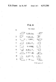
- FIGS. 1 to 6 are views to illustrate the principle of operation of an apparatus according to the invention, wherein FIG. 1 shows a variety of input graphic patterns and FIGS. 2 to 6 illustrate processes of decomposition effected at cascaded unit circuit stages in succession;
- FIG. 7 shows in a block diagram an EB exposure system according to an embodiment of the invention.
- FIG. 8 is a schemetic circuit diagram of a comparison circuit employed in the circuit arrangement shown in FIG. 7;
- FIG. 9 is a circuit diagram showing in detail an arithmetic operation circuit employed in the circuit arrangement shown in FIG. 7.
- the pattern to be depicted is a given one of various trapezoidal patterns, including parallelogram graphic patterns fundamentally composed of sides of vertical, lateral and 45° slanted directions.
- all the graphic patterns to be written are limited to rectangular patterns of dimensions falling within a predetermined size. Accordingly, all the graphic patterns shown in FIG. 1 must be decomposed into smaller rectangular patterns each having long sides L 1 and short sides L 2 which are not greater than respective predetermined lengths and in which L 1 ⁇ L 2 .
- a process of decomposing a trapezoidal pattern into smaller rectangular patterns or sub-patterns will be described.
- the decomposition is effected fundamentally at three steps or stages.
- a trapezoidal pattern to be depicted or written is sliced into elongated patterns.
- the input graphic pattern to be exposed has a pair of sides which extend in parallel with each other either in the lateral (horizontal) or vertical direction, a pattern elongated along the parallel sides is first cut out from the input pattern.
- FIG. 2 A typical processing for the cutout of an elongated sub-pattern is illustrated in FIG. 2.
- an elongated pattern is cut out from the trapezoidal pattern along the bottom side thereof and transferred to a second stage or step.
- the upper remaining portion of the input or original trapezoidal pattern replaces the latter at the first processing stage and again undergoes a similar decomposition process.
- H and W represent, respectively, the height and the width of the original input graphic pattern
- X and Y denote coordinates of the same at the lower left corner
- L 2 represents the height of the elongated sub-pattern to be cut out
- H" and W represent, respectively, the height and the width of the elongated pattern
- X" and Y denote the coordinates of the elongated pattern
- H' and W' represent, respectively, the height and the width of the residual pattern portion which is left behind after the decomposition
- X' and Y' denote the coordinates of the residual pattern portion.
- each of the graphic patterns numbered 1 to 9 can be decomposed into elongated patterns each having a width not greater than L 2 and extending along the horizontal direction in the first stage, while the patterns 10 to 18 are decomposed into elongated patterns in the vertical direction, each of the elongated patterns also having a width not greater than L 2 .
- a triangular portion located at one end or both end portions of the elongated pattern is cut out from the latter.
- the elongated pattern presents a parallelogram
- the parallelogram is decomposed into smaller parallelograms each having a width not greater than L 1 , as will be described hereinafter.
- FIG. 3 illustrates a typical example of the processings performed in the second stage.
- the residual pattern portion shown at the righthand side is again subjected to the decomposition process except for the case where no further decomposition is found to be necessary from the results of comparisons of the parameters N, W and H.
- the data obtained in the second stage is transferred to the third stage, and another input pattern data is supplied or transferred from the first stage.
- FIG. 4 there are illustrated conditions for the decomposition required in the second stage, which conditions differ from one another in dependence on the identifying number of the input pattern.
- the second stage it is discriminated whether decomposition is required or not in accordance with the conditions illustrated in FIG. 4.
- decomposition is necessary, addition and/or subtraction processings are performed on the parameters W, H, X and Y in the manner similar to those in the first stage to provide data of a triangle and the residual pattern after the decomposition.
- the third stage is the final stage of decomposition.
- the condition for the required decomposition is W>L 1 , wherein the decomposition processing is effected in the same manner as in the first stage.
- the patterns other than rectangles each of which includes necessarily at least one oblique side has to be decomposed into a group of smaller rectangles which approximate as a whole the oblique side.
- a number of the smaller divided rectangles are generated on the basis of the input pattern by making use of the oblique side decomposing width L 3 as a parameter in the third stage.
- FIG. 6 A typical example of the above processing is illustrated in FIG. 6.
- a triangle input pattern is decomposed into elongated patterns each having a width L 3 from and along the bottom side so far as the condition that H>L 3 is met.
- the data of the elongated pattern cut out from the bottom portion of the input pattern is transferred to an electron beam exposure unit as depictable pattern data, while the residual upper pattern portion is again supplied to the input of the third stage.
- the processings performed in the first to the third stages may be so combined that the processings at the respective stages can be effected in parallel (in pipeline) and that a new processing in one stage is suspended until the processing in the succeeding stage has been completed. Then, the input pattern data is sequentially transferred from the first stage to the third stage.
- FIG. 7 shows in a block diagram an EB exposure system according to an exemplary embodiment of the invention which is adapted to decompose an input graphic pattern in three stages in the manner described above.
- the circuit stages are of an identical arrangement with one another. Accordingly, the following description will be limited to the circuit arrangement and operation of a single stage.
- a data register 1 is adapted to store therein that data which relates to the shape identification number N, width W, height H and coordinates (X, Y) of an input graphic pattern.
- the data loaded in the data register 1 is constituted by either the output data supplied from the preceding stage or the residual pattern data remaining after decomposition effected by the very stage to which that data register belongs as will be described hereinafter in more detail.
- the data stored in the data register 1 is read out at the timing of a timing clock signal C P .
- the graphic pattern identifying number N contained in the data register 1 is supplied to a control circuit 2 by way of a signal line 11, while a comparison command signal corresponding to the pattern identifying number N is supplied to a comparison circuit 3 through a signal line 12.
- the comparison circuit 3 has inputs supplied with the data signals representative of the width W and the height H of the input pattern from the data register 1 by way of a signal line 13 and the other input externally supplied with the decomposition width parameters L 1 , L 2 and L 3 (hereinafter denoted generally by L).
- the comparator circuit 3 thus performs desired comparison processings by making use of the input pattern parameters W and H and the decomposition width parameter L in accordance with the comparison command supplied through the signal line 12 to thereby arithmetically derive the conditions on which the input pattern is to be decomposed.
- the results of the comparison are then supplied to the control circuit 2 through a signal line 14.
- the control circuit 2 in turn discriminates on the basis of the results of the comparison whether the input pattern be decomposed or not.
- the contents of arithmetic operations to be effected by arithmetic operation circuits 4 and 5 are determined in dependence on the input pattern identifying number N, whereby corresponding control signals are supplied to the arithmetic operation circuits 4 and 5 through signal lines 15 and 16. Further, the data signals N, W, H and (X, Y) read out from the data register 1 are inputted to the arithmetic operation circuits 4 and 5 through signal lines 17 and 18, respectively, while the decomposition width parameter L is externally supplied to the circuits 4 and 5.
- the arithmetic operation circuit 4 calculates the one hand, the residual pattern data on the basis of the input data, the result of the calculation is again transferred to the data register 1 through signal lines 19 and 20 and a selector circuit 6 to update the contents of the data register 1.
- the arithemtic operation circuit 5 arithmetically derives the data of a cut out pattern, which data is supplied to the following selector circuit 6 constituting a part of the following stage and is stored in the data register 1 of that stage.
- the processings mentioned above are performed when the control circuit 2 discriminates that the decomposition is necessary.
- a corresponding control signal is supplied to the arithmetic operation circuit 5 through a signal line 16, as a result of which the input pattern data N, W, H and (X, Y) in the data register 1 are transferred, as they are, to the selector circuit 6 of the succeeding stage through the arithmetic operation circuit 5 and a signal line 21.
- a change-over or switching signal is supplied to the selector circuit 6 through a signal line 22 to cause the selector circuit 6 to be changed over to the state in which the pattern data outputted from the preceding stage is allowed to be loaded in the data register 1 of the present stage.
- the control circuit 2 of the preceding stage then responds to the wait or standby signal to suspend the new operation of the associated arithmetic circuit 5 and at the same time causes the data outputted from the associated data register 1 to be again loaded in that register 1, as they are, through the arithmetic operation unit 4.
- each of the control circuits 2 may be realized by a well known read-only memory (ROM) element which is capable of producing output signals corresponding to combinations of various input signals, respectively.
- ROM read-only memory
- comparison circuit 3 may be realized in such a configuration as shown in FIG. 8, by way of example.
- a multiplexer 31 selects the desired data from the data W and H available from the data register 1 shown in FIG. 7 and the externally supplied data L, and supplies the desired data in dependence on the signal N representing the shape of the input pattern and supplied from the control circuit 2 also shown in FIG. 7.
- circuit arrangement may be made such that data signals representative of W/2, H/2 and L/2 or 2W, 2H and 2L corresponding to a bit shift of the data, respectively, can also be selected.
- a comparator 32 receives the output from the multiplexer circuit 31 to perform comparison, the result of which is supplied to the control circuit 2 shown in FIG. 7.
- the multiplexer circuit 31 selects the data W and H which are then supplied to the comparator 32 where magnitudes of these data are compared to each other to produce a corresponding output signal.
- the arithmetic operation circuit 4 or 5 shown in FIG. 7 may be realized in a configuration shown in FIG. 9, by way of example.
- reference numerals 41 and 42 denote multiplexers, 43 and 44 denote adders, 45 and 46 denote Exclusive-OR circuits each circuit including a plurality of Exclusive-OR's, and 47 denotes a gate circuit.
- the pattern data W and Y resulting from the decomposition are generated.
- the pattern data H and X can be generated by a similar circuit not shown.
- Each of the multiplexers 41 and 42 has the inputs supplied with the data W, H, X and Y from the data register shown in FIG. 7 and the data L applied externally, and selects the desired ones from these input data in dependence on control signal CS1 or CS2 supplied from the control circuit 2 shown in FIG. 7 for outputting the selected data after having been shifted, if necessary.
- the output data from the multiplexers 41 and 42 is applied to the adders 43 and 44 and the Exclusive-OR circuit 45 and 46, respectively.
- the Exclusive-OR circuits 45 and 46 have the inputs supplied with control signals CS3 and CS4, respectively, from the control circuit 2 shown in FIG. 7. These control signals serve to invert the respective input data through the Exclusive-OR's in each Exclusive-OR circuit.
- the pattern data W, H, X and Y of the decomposed pattern is obtained.
- the gate circuit 47 has its input supplied with the data W, H, X, Y and N from the data register 1. This input data is outputted from the gate circuit 47 without modification in response to a control signal CS5 supplied from the control circuit 2.
- the gate circuit 47 allows the input data to pass therethrough as it is, when it is discriminated by the control circuit 2 that no decomposition is required or when the wait signal is issued from the succeeding stage.
- a signal NS representative of the pattern type identification of the decomposed or cut out pattern is supplied to the arithmetic operation circuit from the control circuit 2 and outputted as it is.
- trapezoidal patterns are decomposed in three stages.
- the slanted side is assumed to form 45° with respect to the horizontal and vertical axes.
- the invention is never restricted to the illustrated number of the stages nor to the illustrated manner of decomposition. Rather, the decomposition processing may be carried out at a desired number of stages in dependence on the shapes of the input patterns and/or on different discrimination criteria. Also the angle of the slanted side is not limited to 45°. Calculations for such patterns will be apparent to those skilled in the art.
- the present invention makes it possible to decompose input graphic patterns of various shape by means of a common circuit with a simplified circuit arrangement. Further, the processing for pattern decomposition can be accomplished at a very high speed by virtue of such arrangement that the processing is realized in a plurality of processing stages in a pipeline arrangement.
- the invention thus provides pattern decomposing processing at an extremely high speed with a simplified circuit structure.
- an electron beam having a rectangular cross-section of a given adjustable size is formed in dependence on decomposed pattern data and successive exposure of the decomposed pattern is accomplished by respective single irradiations of the electron beam to form a desired pattern.
Abstract
Description
N→N'
H-L.sub.2 →H'
W-L.sub.2 →W'
X+L.sub.2 →X'
Y+L.sub.2 →Y'
N→N"
L.sub.2 →H"
W→W"
X→X"
Y→Y"
N→N'
H-L.sub.3 →H'
W-L.sub.3 →W'
X+L.sub.3 →X'
Y+L.sub.3 →Y'
L.sub.3 →H"
W-L.sub.3 /2→W"
X+L.sub.3 /2→X"
Y→Y"
Claims (13)
Applications Claiming Priority (2)
| Application Number | Priority Date | Filing Date | Title |
|---|---|---|---|
| JP56-88183 | 1981-06-10 | ||
| JP56088183A JPS57204125A (en) | 1981-06-10 | 1981-06-10 | Electron-ray drawing device |
Publications (1)
| Publication Number | Publication Date |
|---|---|
| US4532598A true US4532598A (en) | 1985-07-30 |
Family
ID=13935786
Family Applications (1)
| Application Number | Title | Priority Date | Filing Date |
|---|---|---|---|
| US06/386,301 Expired - Lifetime US4532598A (en) | 1981-06-10 | 1982-06-08 | Electron beam exposure system |
Country Status (5)
| Country | Link |
|---|---|
| US (1) | US4532598A (en) |
| EP (1) | EP0066882B1 (en) |
| JP (1) | JPS57204125A (en) |
| AT (1) | ATE60958T1 (en) |
| DE (1) | DE3280306D1 (en) |
Cited By (25)
| Publication number | Priority date | Publication date | Assignee | Title |
|---|---|---|---|---|
| US4837447A (en) * | 1986-05-06 | 1989-06-06 | Research Triangle Institute, Inc. | Rasterization system for converting polygonal pattern data into a bit-map |
| US4878177A (en) * | 1987-02-16 | 1989-10-31 | Kabushiki Kaisha Toshiba | Method for drawing a desired circuit pattern using charged particle beam |
| US4989156A (en) * | 1985-08-23 | 1991-01-29 | Kabushiki Kaisha Toshiba | Method of drawing a pattern on wafer with charged beam |
| US5030836A (en) * | 1988-08-05 | 1991-07-09 | Toshiba Machine Co., Ltd. | Method and apparatus for drawing patterns using an energy beam |
| US5159201A (en) * | 1991-07-26 | 1992-10-27 | International Business Machines Corporation | Shape decompositon system and method |
| US5210696A (en) * | 1989-02-10 | 1993-05-11 | Fujitsu Limited | Electron beam exposure data processing method, electron beam exposure method and apparatus |
| US5251140A (en) * | 1991-07-26 | 1993-10-05 | International Business Machines Corporation | E-beam control data compaction system and method |
| US5428552A (en) * | 1991-10-08 | 1995-06-27 | International Business Machines Corporation | Data compaction techniques for generation of a complex image |
| US5434795A (en) * | 1990-01-11 | 1995-07-18 | Fujitsu Limited | Method of forming pattern having optical angle in charged particle exposure system |
| US5500930A (en) * | 1988-11-04 | 1996-03-19 | Fujitsu Limited | System to decode instructions indicating the addresses of control codes and providing patterns to direct an electron beam exposure apparatus |
| US5563419A (en) * | 1994-05-25 | 1996-10-08 | Nec Corporation | Electron beam exposure system capable of correcting proximity effect |
| US5812412A (en) * | 1995-04-28 | 1998-09-22 | Mitsubishi Denki Kabushiki Kaisha | Charged beam pattern data generating method and a charged beam pattern data generating apparatus |
| US6060716A (en) * | 1997-03-28 | 2000-05-09 | Jeol Ltd. | Electron beam lithography method |
| US6275604B1 (en) * | 1998-03-16 | 2001-08-14 | Fujitsu Limited | Method and apparatus for generating semiconductor exposure data |
| US20020129324A1 (en) * | 1992-03-31 | 2002-09-12 | Iadonato Kevin R. | Integrated structure layout and layout of interconnections for an instruction execution unit of an integrated circuit chip |
| US20030107008A1 (en) * | 2001-10-26 | 2003-06-12 | Jeol Ltd. | Lithographic method using variable-area electron-beam lithography machine |
| US20050233227A1 (en) * | 2004-04-14 | 2005-10-20 | Baorui Yang | Methods for improving angled line feature accuracy and throughput using electron beam lithography and electron beam lithography system |
| US7516305B2 (en) | 1992-05-01 | 2009-04-07 | Seiko Epson Corporation | System and method for retiring approximately simultaneously a group of instructions in a superscalar microprocessor |
| US7558945B2 (en) | 1992-12-31 | 2009-07-07 | Seiko Epson Corporation | System and method for register renaming |
| US7685402B2 (en) | 1991-07-08 | 2010-03-23 | Sanjiv Garg | RISC microprocessor architecture implementing multiple typed register sets |
| US7739482B2 (en) | 1991-07-08 | 2010-06-15 | Seiko Epson Corporation | High-performance, superscalar-based computer system with out-of-order instruction execution |
| US7802074B2 (en) | 1992-03-31 | 2010-09-21 | Sanjiv Garg | Superscalar RISC instruction scheduling |
| US8074052B2 (en) | 1992-12-31 | 2011-12-06 | Seiko Epson Corporation | System and method for assigning tags to control instruction processing in a superscalar processor |
| US20160118221A1 (en) * | 2014-10-27 | 2016-04-28 | Canon Kabushiki Kaisha | Lithography system and method of manufacturing articles |
| US20160126062A1 (en) * | 2014-10-27 | 2016-05-05 | Canon Kabushiki Kaisha | Drawing apparatus, lithography system, pattern data creation method, drawing method, and method of manufacturing articles |
Families Citing this family (6)
| Publication number | Priority date | Publication date | Assignee | Title |
|---|---|---|---|---|
| JPS60196939A (en) * | 1984-03-19 | 1985-10-05 | Fujitsu Ltd | Charged particle beam exposure |
| JP2680295B2 (en) * | 1984-03-22 | 1997-11-19 | 株式会社東芝 | Method and apparatus for drawing data of electron beam exposure apparatus |
| JP2710162B2 (en) * | 1988-12-13 | 1998-02-10 | 株式会社東芝 | Method and apparatus for creating charged beam drawing data |
| US5446649A (en) * | 1992-12-31 | 1995-08-29 | International Business Machines Corporation | Data-hiding and skew scan for unioning of shapes in electron beam lithography post-processing |
| GB2334597B (en) * | 1995-04-28 | 1999-11-17 | Mitsubishi Electric Corp | A charged beam pattern data generating method and a charged beam pattern data generating apparatus |
| JP5658997B2 (en) * | 2010-12-17 | 2015-01-28 | 株式会社ニューフレアテクノロジー | Charged particle beam drawing apparatus and drawing data generation method |
Citations (10)
| Publication number | Priority date | Publication date | Assignee | Title |
|---|---|---|---|---|
| US3894271A (en) * | 1973-08-31 | 1975-07-08 | Ibm | Method and apparatus for aligning electron beams |
| US4145597A (en) * | 1975-12-31 | 1979-03-20 | Fujitsu Limited | Electron beam lithographic system |
| US4147937A (en) * | 1977-11-01 | 1979-04-03 | Fujitsu Limited | Electron beam exposure system method and apparatus |
| US4151422A (en) * | 1977-06-30 | 1979-04-24 | Rikagaku Kenkyusho | Electron beam exposure method |
| US4167676A (en) * | 1978-02-21 | 1979-09-11 | Bell Telephone Laboratories, Incorporated | Variable-spot scanning in an electron beam exposure system |
| US4213053A (en) * | 1978-11-13 | 1980-07-15 | International Business Machines Corporation | Electron beam system with character projection capability |
| US4280186A (en) * | 1978-07-07 | 1981-07-21 | Tokyo Shibaura Denki Kabushiki Kaisha | Exposure apparatus using electron beams |
| US4291231A (en) * | 1977-12-30 | 1981-09-22 | Fujitsu Limited | Electron beam exposure system and an apparatus for carrying out the same |
| US4393312A (en) * | 1976-02-05 | 1983-07-12 | Bell Telephone Laboratories, Incorporated | Variable-spot scanning in an electron beam exposure system |
| US4424448A (en) * | 1979-12-26 | 1984-01-03 | Tokyo Shibaura Denki Kabushiki Kaisha | Electron beam apparatus |
Family Cites Families (2)
| Publication number | Priority date | Publication date | Assignee | Title |
|---|---|---|---|---|
| JPS5473577A (en) * | 1977-11-24 | 1979-06-12 | Fujitsu Ltd | Electron beam exposure method |
| JPS5712520A (en) * | 1980-06-26 | 1982-01-22 | Nippon Telegr & Teleph Corp <Ntt> | Dividing method of figure by exposing in electron beam radiation |
-
1981
- 1981-06-10 JP JP56088183A patent/JPS57204125A/en active Granted
-
1982
- 1982-06-08 DE DE8282105022T patent/DE3280306D1/en not_active Expired - Lifetime
- 1982-06-08 EP EP82105022A patent/EP0066882B1/en not_active Expired - Lifetime
- 1982-06-08 AT AT82105022T patent/ATE60958T1/en not_active IP Right Cessation
- 1982-06-08 US US06/386,301 patent/US4532598A/en not_active Expired - Lifetime
Patent Citations (10)
| Publication number | Priority date | Publication date | Assignee | Title |
|---|---|---|---|---|
| US3894271A (en) * | 1973-08-31 | 1975-07-08 | Ibm | Method and apparatus for aligning electron beams |
| US4145597A (en) * | 1975-12-31 | 1979-03-20 | Fujitsu Limited | Electron beam lithographic system |
| US4393312A (en) * | 1976-02-05 | 1983-07-12 | Bell Telephone Laboratories, Incorporated | Variable-spot scanning in an electron beam exposure system |
| US4151422A (en) * | 1977-06-30 | 1979-04-24 | Rikagaku Kenkyusho | Electron beam exposure method |
| US4147937A (en) * | 1977-11-01 | 1979-04-03 | Fujitsu Limited | Electron beam exposure system method and apparatus |
| US4291231A (en) * | 1977-12-30 | 1981-09-22 | Fujitsu Limited | Electron beam exposure system and an apparatus for carrying out the same |
| US4167676A (en) * | 1978-02-21 | 1979-09-11 | Bell Telephone Laboratories, Incorporated | Variable-spot scanning in an electron beam exposure system |
| US4280186A (en) * | 1978-07-07 | 1981-07-21 | Tokyo Shibaura Denki Kabushiki Kaisha | Exposure apparatus using electron beams |
| US4213053A (en) * | 1978-11-13 | 1980-07-15 | International Business Machines Corporation | Electron beam system with character projection capability |
| US4424448A (en) * | 1979-12-26 | 1984-01-03 | Tokyo Shibaura Denki Kabushiki Kaisha | Electron beam apparatus |
Non-Patent Citations (2)
| Title |
|---|
| Fujinami et al., Precision Electron Beam Exposure System EB 52, Review of the Electrical Communications Laboratories, vol. 27, 1 2, (1,2/79), pp. 97 104. * |
| Fujinami et al., Precision Electron Beam Exposure System EB52, Review of the Electrical Communications Laboratories, vol. 27, #1-2, (1,2/79), pp. 97-104. |
Cited By (43)
| Publication number | Priority date | Publication date | Assignee | Title |
|---|---|---|---|---|
| US4989156A (en) * | 1985-08-23 | 1991-01-29 | Kabushiki Kaisha Toshiba | Method of drawing a pattern on wafer with charged beam |
| US4837447A (en) * | 1986-05-06 | 1989-06-06 | Research Triangle Institute, Inc. | Rasterization system for converting polygonal pattern data into a bit-map |
| US4878177A (en) * | 1987-02-16 | 1989-10-31 | Kabushiki Kaisha Toshiba | Method for drawing a desired circuit pattern using charged particle beam |
| US5030836A (en) * | 1988-08-05 | 1991-07-09 | Toshiba Machine Co., Ltd. | Method and apparatus for drawing patterns using an energy beam |
| US5500930A (en) * | 1988-11-04 | 1996-03-19 | Fujitsu Limited | System to decode instructions indicating the addresses of control codes and providing patterns to direct an electron beam exposure apparatus |
| US5210696A (en) * | 1989-02-10 | 1993-05-11 | Fujitsu Limited | Electron beam exposure data processing method, electron beam exposure method and apparatus |
| US5434795A (en) * | 1990-01-11 | 1995-07-18 | Fujitsu Limited | Method of forming pattern having optical angle in charged particle exposure system |
| US7941636B2 (en) | 1991-07-08 | 2011-05-10 | Intellectual Venture Funding Llc | RISC microprocessor architecture implementing multiple typed register sets |
| US7685402B2 (en) | 1991-07-08 | 2010-03-23 | Sanjiv Garg | RISC microprocessor architecture implementing multiple typed register sets |
| US7739482B2 (en) | 1991-07-08 | 2010-06-15 | Seiko Epson Corporation | High-performance, superscalar-based computer system with out-of-order instruction execution |
| US5251140A (en) * | 1991-07-26 | 1993-10-05 | International Business Machines Corporation | E-beam control data compaction system and method |
| US5159201A (en) * | 1991-07-26 | 1992-10-27 | International Business Machines Corporation | Shape decompositon system and method |
| US5428552A (en) * | 1991-10-08 | 1995-06-27 | International Business Machines Corporation | Data compaction techniques for generation of a complex image |
| US20040243961A1 (en) * | 1992-03-31 | 2004-12-02 | Seiko Epson Corporation | Integrated structure layout and layout of interconnections for an instruction execution unit of an integrated circuit chip |
| US20070113214A1 (en) * | 1992-03-31 | 2007-05-17 | Seiko Epson Corporation | Integrated structure layout and layout of interconnections for an instruction execution unit of an integrated circuit chip |
| US7555738B2 (en) | 1992-03-31 | 2009-06-30 | Seiko Epson Corporation | Integrated structure layout and layout of interconnections for an instruction execution unit of an integrated circuit chip |
| US20020129324A1 (en) * | 1992-03-31 | 2002-09-12 | Iadonato Kevin R. | Integrated structure layout and layout of interconnections for an instruction execution unit of an integrated circuit chip |
| US6782521B2 (en) * | 1992-03-31 | 2004-08-24 | Seiko Epson Corporation | Integrated structure layout and layout of interconnections for an instruction execution unit of an integrated circuit chip |
| US7174525B2 (en) | 1992-03-31 | 2007-02-06 | Seiko Epson Corporation | Integrated structure layout and layout of interconnections for an instruction execution unit of an integrated circuit chip |
| US7802074B2 (en) | 1992-03-31 | 2010-09-21 | Sanjiv Garg | Superscalar RISC instruction scheduling |
| US7523296B2 (en) | 1992-05-01 | 2009-04-21 | Seiko Epson Corporation | System and method for handling exceptions and branch mispredictions in a superscalar microprocessor |
| US7934078B2 (en) | 1992-05-01 | 2011-04-26 | Seiko Epson Corporation | System and method for retiring approximately simultaneously a group of instructions in a superscalar microprocessor |
| US7958337B2 (en) | 1992-05-01 | 2011-06-07 | Seiko Epson Corporation | System and method for retiring approximately simultaneously a group of instructions in a superscalar microprocessor |
| US7516305B2 (en) | 1992-05-01 | 2009-04-07 | Seiko Epson Corporation | System and method for retiring approximately simultaneously a group of instructions in a superscalar microprocessor |
| US7979678B2 (en) | 1992-12-31 | 2011-07-12 | Seiko Epson Corporation | System and method for register renaming |
| US8074052B2 (en) | 1992-12-31 | 2011-12-06 | Seiko Epson Corporation | System and method for assigning tags to control instruction processing in a superscalar processor |
| US7558945B2 (en) | 1992-12-31 | 2009-07-07 | Seiko Epson Corporation | System and method for register renaming |
| US5563419A (en) * | 1994-05-25 | 1996-10-08 | Nec Corporation | Electron beam exposure system capable of correcting proximity effect |
| US5812412A (en) * | 1995-04-28 | 1998-09-22 | Mitsubishi Denki Kabushiki Kaisha | Charged beam pattern data generating method and a charged beam pattern data generating apparatus |
| US6060716A (en) * | 1997-03-28 | 2000-05-09 | Jeol Ltd. | Electron beam lithography method |
| US6275604B1 (en) * | 1998-03-16 | 2001-08-14 | Fujitsu Limited | Method and apparatus for generating semiconductor exposure data |
| US6753540B2 (en) * | 2001-10-26 | 2004-06-22 | Jeol Ltd. | Lithographic method using variable-area electron-beam lithography machine |
| US20030107008A1 (en) * | 2001-10-26 | 2003-06-12 | Jeol Ltd. | Lithographic method using variable-area electron-beam lithography machine |
| US7759660B2 (en) | 2004-04-14 | 2010-07-20 | Micron Technology, Inc. | Electron beam lithography system |
| US20050233227A1 (en) * | 2004-04-14 | 2005-10-20 | Baorui Yang | Methods for improving angled line feature accuracy and throughput using electron beam lithography and electron beam lithography system |
| US7229742B2 (en) | 2004-04-14 | 2007-06-12 | Micron Technology, Inc. | Methods for improving angled line feature accuracy and throughput using electron beam lithography and electron beam lithography system |
| US20070003874A1 (en) * | 2004-04-14 | 2007-01-04 | Baorui Yang | Methods for improving angled line feature accuracy and throughput using electron beam lithography and electron beam lithography system |
| US20070102651A1 (en) * | 2004-04-14 | 2007-05-10 | Baorui Yang | Methods for improving angled line feature accuracy and throughput using electron beam lithography and electron beam lithography system |
| US7226723B2 (en) | 2004-04-14 | 2007-06-05 | Micron Technology, Inc. | Methods for improving angled line feature accuracy and throughput using electron beam lithography and electron beam lithography system |
| US20160118221A1 (en) * | 2014-10-27 | 2016-04-28 | Canon Kabushiki Kaisha | Lithography system and method of manufacturing articles |
| US20160126062A1 (en) * | 2014-10-27 | 2016-05-05 | Canon Kabushiki Kaisha | Drawing apparatus, lithography system, pattern data creation method, drawing method, and method of manufacturing articles |
| US9558916B2 (en) * | 2014-10-27 | 2017-01-31 | Canon Kabushiki Kaisha | Lithography system and method of manufacturing articles |
| US9583311B2 (en) * | 2014-10-27 | 2017-02-28 | Canon Kabushiki Kaisha | Drawing apparatus, lithography system, pattern data creation method, drawing method, and method of manufacturing articles |
Also Published As
| Publication number | Publication date |
|---|---|
| ATE60958T1 (en) | 1991-03-15 |
| JPS6239818B2 (en) | 1987-08-25 |
| JPS57204125A (en) | 1982-12-14 |
| EP0066882B1 (en) | 1991-02-20 |
| EP0066882A2 (en) | 1982-12-15 |
| DE3280306D1 (en) | 1991-03-28 |
| EP0066882A3 (en) | 1985-06-05 |
Similar Documents
| Publication | Publication Date | Title |
|---|---|---|
| US4532598A (en) | Electron beam exposure system | |
| EP0298275B1 (en) | Pattern splicing system and method for scanning of electron beam system | |
| EP0002957B1 (en) | Electron beam exposure apparatus | |
| US4259724A (en) | Device comprising a circuit for making a beam exposure system effectively draw a repetitive pattern | |
| EP0104922A2 (en) | Electron beam exposure system | |
| US20050285054A1 (en) | Charged particle beam drawing apparatus | |
| JP4054445B2 (en) | Charged beam drawing method | |
| US20170018404A1 (en) | Drawing data creation method and charged particle beam drawing apparatus | |
| JPS59136874A (en) | Pattern identifier | |
| JP3159810B2 (en) | Electron beam drawing method and apparatus | |
| US6314554B1 (en) | Method of generating mask pattern data for graphics and apparatus for the same | |
| US5206517A (en) | Electron beam lithographic method | |
| JP2661739B2 (en) | Electron beam exposure method | |
| US6535222B1 (en) | Graphic method | |
| JP3983188B2 (en) | Parallel processing method of inverse matrix for shared memory type scalar parallel computer | |
| JP3408010B2 (en) | Pattern developing method and apparatus for charged particle beam exposure apparatus | |
| JP2697943B2 (en) | Processing method of writing data in charged particle beam writing | |
| JPH04137614A (en) | Method of lithography using charged beam | |
| Mlekus et al. | Polygonal geometry reconstruction after cellular etching or deposition simulation | |
| JPS6390827A (en) | Method and equipment of charged particle beam lithography | |
| JP2857260B2 (en) | Judgment method of rectangular area | |
| JPS58155474A (en) | Drawing method of parallel curve | |
| JPH11329958A (en) | Charged particle beam aligner | |
| JPH01152726A (en) | Charged particle beam lithography | |
| JP3083573B2 (en) | How to create charged beam drawing data |
Legal Events
| Date | Code | Title | Description |
|---|---|---|---|
| AS | Assignment |
Owner name: NIPPON TELEGRAPH & TELEPHONE PUBLIC CORPORATION Free format text: ASSIGNMENT OF ASSIGNORS INTEREST.;ASSIGNORS:SHIBAYAMA, AKINORI;FUJINAMI, MINPAI;YODA, HARUO;REEL/FRAME:004011/0429 Effective date: 19820601 Owner name: HITACHI, LTD. Free format text: ASSIGNMENT OF ASSIGNORS INTEREST.;ASSIGNORS:SHIBAYAMA, AKINORI;FUJINAMI, MINPAI;YODA, HARUO;REEL/FRAME:004011/0429 Effective date: 19820601 |
|
| STCF | Information on status: patent grant |
Free format text: PATENTED CASE |
|
| AS | Assignment |
Owner name: NIPPON TELEGRAPH & TELEPHONE CORPORATION Free format text: CHANGE OF NAME;ASSIGNOR:NIPPON TELEGRAPH AND TELEPHONE PUBLIC CORPORATION;REEL/FRAME:004454/0001 Effective date: 19850718 |
|
| FPAY | Fee payment |
Year of fee payment: 4 |
|
| FEPP | Fee payment procedure |
Free format text: PAYOR NUMBER ASSIGNED (ORIGINAL EVENT CODE: ASPN); ENTITY STATUS OF PATENT OWNER: LARGE ENTITY |
|
| FPAY | Fee payment |
Year of fee payment: 8 |
|
| FPAY | Fee payment |
Year of fee payment: 12 |