US4545002A - Thyristor voltage limiter for current source inverter - Google Patents
Thyristor voltage limiter for current source inverter Download PDFInfo
- Publication number
- US4545002A US4545002A US06/508,712 US50871283A US4545002A US 4545002 A US4545002 A US 4545002A US 50871283 A US50871283 A US 50871283A US 4545002 A US4545002 A US 4545002A
- Authority
- US
- United States
- Prior art keywords
- thyristors
- inverter
- controlling
- current
- voltage
- Prior art date
- Legal status (The legal status is an assumption and is not a legal conclusion. Google has not performed a legal analysis and makes no representation as to the accuracy of the status listed.)
- Expired - Fee Related
Links
Images


Classifications
-
- H—ELECTRICITY
- H02—GENERATION; CONVERSION OR DISTRIBUTION OF ELECTRIC POWER
- H02M—APPARATUS FOR CONVERSION BETWEEN AC AND AC, BETWEEN AC AND DC, OR BETWEEN DC AND DC, AND FOR USE WITH MAINS OR SIMILAR POWER SUPPLY SYSTEMS; CONVERSION OF DC OR AC INPUT POWER INTO SURGE OUTPUT POWER; CONTROL OR REGULATION THEREOF
- H02M5/00—Conversion of ac power input into ac power output, e.g. for change of voltage, for change of frequency, for change of number of phases
- H02M5/40—Conversion of ac power input into ac power output, e.g. for change of voltage, for change of frequency, for change of number of phases with intermediate conversion into dc
- H02M5/42—Conversion of ac power input into ac power output, e.g. for change of voltage, for change of frequency, for change of number of phases with intermediate conversion into dc by static converters
- H02M5/44—Conversion of ac power input into ac power output, e.g. for change of voltage, for change of frequency, for change of number of phases with intermediate conversion into dc by static converters using discharge tubes or semiconductor devices to convert the intermediate dc into ac
- H02M5/443—Conversion of ac power input into ac power output, e.g. for change of voltage, for change of frequency, for change of number of phases with intermediate conversion into dc by static converters using discharge tubes or semiconductor devices to convert the intermediate dc into ac using devices of a thyratron or thyristor type requiring extinguishing means
- H02M5/45—Conversion of ac power input into ac power output, e.g. for change of voltage, for change of frequency, for change of number of phases with intermediate conversion into dc by static converters using discharge tubes or semiconductor devices to convert the intermediate dc into ac using devices of a thyratron or thyristor type requiring extinguishing means using semiconductor devices only
- H02M5/4505—Conversion of ac power input into ac power output, e.g. for change of voltage, for change of frequency, for change of number of phases with intermediate conversion into dc by static converters using discharge tubes or semiconductor devices to convert the intermediate dc into ac using devices of a thyratron or thyristor type requiring extinguishing means using semiconductor devices only having a rectifier with controlled elements
Abstract
A voltage limiter for protecting the thyristors of a current source inverter, also known as a controlled current inverter, wherein the limiter includes a circuit for sensing the respective voltages directly across at least one but preferably across each of the thyristors in the inverter and generating a signal corresponding to the highest value and a regulator circuit which is operable in response to the difference between the highest value signal and a reference signal corresponding to a safe operating voltage for the thyristors in the inverter, to modify the thyristor gating angle of those thyristors which control the current in the inverter. The voltage limiter thus reduces the current carried by the inverter thyristors when the highest voltage across the inverter thyristors exceeds the reference signal, and thereby reduces the amplitude of any commutating spike voltage in the voltage applied across the thyristors. This permits full utilization of the inverter rating while requiring no adjustment for source impedance, line voltage, or commutating capacitance.
Description
This application is related to the following applications, which are assigned to the assignee of the present invention and which are herein meant to be incorporated by reference:
U.S. Pat. No. 4,496,899, "Control For A Force Commutated Current Source VAR Generator", issued Jan. 29, 1985, in the name of Loren H. Walker and David L. Lippitt; and
U.S. Ser. No. 508,711, entitled, "Capacitance Control For A Static VAR Generator", filed on June 28, 1983, in the name of Loren H. Walker.
This invention relates generally to current source inverters, also known as controlled current inverters, and more particularly to a method and means for limiting the voltage on the thyristors of a current source thyristor inverter.
In U.S. Pat. No. 4,230,979, entitled, "Controlled Current Inverter And Motor Control System", issued to Paul M. Espelage, et al. on Oct. 28, 1980, and assigned to the present assignee, there is disclosed a typical example of a current source inverter motor drive system including a thyristor type current source inverter.
The peak voltage on the thyristors of a current source inverter is proportional to the sum of the peak value of the sinusoidal voltage applied to the alternating current (AC) terminals of the inverter and the value of direct current (DC) commutated by the inverter. Prior art techniques utilized for limiting this voltage include power level clamps or surge suppressors to limit these voltages by force, or by the use of signal level methods to predict this voltage and thereafter limit current to a value which will not produce excessive voltage. U.S. Pat. No. 4,237,531, entitled, "Controlled Current Inverter System Having Semiconductor Overvoltage Protection", issuing to John H. Cutler and Loren H. Walker on Dec. 2, 1980, and assigned to the present assignee, describes not only a controlled current thyristor inverter, but also describes a predictive method and apparatus which transiently interrupts operation of the inverter when overvoltages across the thyristors are predicted. The inventive concept of U.S. Pat. No. 4,237,531 is applicable to thyristors of current source inverters whether used in motor drives as described in U.S. Pat. No. 4,230,979, or in var generators as described in the aforementioned U.S. Pat. No. 4,496,899. The only difference between motor drive and var controller applications is that in the case of the var generator, the thyristors which control the current are the same ones being protected. In an AC motor drive system, the inverter thyristors on the motor side of a DC link, coupling AC to DC source side converter and the motor side DC to AC inverter, are protected by changing the gating time; i.e., the firing angle of the thyristors in the converter connected to the source of AC power, due to the fact that the source side thyristors are the means by which current is controlled.
It is, therefore, an object of the present invention to provide an improvement in current source inverters and their method of operation.
It is a further object to provide an improvement in the control of current source thyristor inverters also known as controlled current inverters.
It is another object of the invention to provide an improved control of a current source inverter operating as a var generator.
It is still another object of the invention to provide an improved control of a current source inverter operating in a motor drive system.
A still further object is to provide a current source inverter which protects against overvoltage conditions as a function of load voltage, current and electrical parameters of the load.
It is yet another object to provide a current source thyristor inverter having means to protect the thyristors from overvoltage conditions.
The foregoing and other objects are achieved, in accordance with the present invention, by measuring the voltage(s) across one or more but preferably each of the individual thyristors of a current source inverter, including any commutating spike voltage, comparing it to a predetermined limit level in the form of a reference voltage and controlling the DC current level so that this voltage does not exceed this limit level. Control of current is achieved by regulating the gating angle of the thyristors which control current in response to the error between inverter thyristor voltage and the reference voltage. Such a control is not only fast acting, but overrides all other controls which attempt to determine current. The advantages of this approach over other known approaches is that it involves no prediction, either of height or phase position of the commutating spike voltage. Thus a motor drive or var generator implemented with current source inverter may be operated smoothly to the limits of thyristor voltage capability, without abrupt transients when this limit is reached and without margins normally required where spike voltage amplitude or phase position are estimated.
While the present invention is defined in the claims annexed to and forming a part of this specification, a better understanding of the invention can be had by reference to the following description taken in conjunction with the accompanying drawings in which:
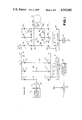
FIG. 1 is an electrical schematic diagram of a basic current source thyristor inverter utilized in a motor drive system in accordance with the known prior art;
FIG. 2 is an electrical schematic diagram of the current source thyristor inverter of FIG. 1 utilized in a var generator system;
FIGS. 3A and 3B are line voltage waveform diagrams helpful in understanding the operation of the subject invention;
FIG. 4 is an electrical schematic diagram illustrative of a thyristor voltage limiter in accordance with the subject invention utilized in the controlled current inverter motor drive system of FIG. 1;
FIG. 5 is an electrical schematic diagram of a thyristor voltage limiter in accordance with the subject invention utilized in the current source inverter var generator system of FIG. 2; and
FIG. 6 is an electrical schematic diagram illustrative of the preferred embodiment of the thyristor voltage limiter circuitry utilized in the systems of FIGS. 4 and 5.
Referring now to the drawings and more particularly to FIG. 1, reference numeral 10 denotes a variable direct current (DC) source which comprises an AC to DC converter including a three phase bridge including six thyristors 121 through 126 which are coupled to and receive alternating current (AC) power from a three phase power source 14 by way of the power lines 16, 18 and 20 connected to bridge circuit junctions 22, 24 and 26. The term thyristor will be used in the remaining portion of this description and is to be expressly understood that this term is used in a generic sense to connote controlled rectifiers generally. As is known in the prior art, the output of the thyristor converter 10 can be made a function of the times at which the thyristors 121 through 126 of the bridge arrangement are gated on with respect to the applied voltage and which is commonly known as phase controlling. The control of thyristors 121 through 126 is a function of gating signals applied to the respective gate electrodes which are supplied from a thyristor firing circuit 27 (only two such connections being shown for sake of simplicity) which is operable to sequentially fire the thyristors at a predetermined delay angle α, measured from the earliest point of natural commutation and which comprises the zero crossing points of the line to line voltages across the lines 16, 18 and 20. The thyristor firing circuit 27, moreover, operates in a well known manner in response to the output of a current regulator circuit 28.
The current regulator circuit 28 typically comprises a proportional plus integral type controller which comprises, for example, an operational amplifier configured to operate as a gain amplifier having a transfer function of ##EQU1## where S is a LaPlace operator, T is a time constant, and K is a gain constant. Furthermore, the current regulator 28 receives as an input control signal the difference or error signal between a current command signal I* and a current feedback signal IFBK appearing at the output of a summing junction 29. The signal IFBK is generated in a manner to be described. It is to be recognized, however, that other forms of the variable DC source can be used with equal facility insofar as the present invention is concerned. The thyristor converter 10 forming the variable DC source supplies a DC current ID to a force commutated thyristor inverter 30 by way of a DC link which comprises suitable conductors 32 and 33 and further including a reactor 34. A current transformer 35 shown connected to line 32 supplies a signal proportional to the DC current ID supplied to the inverter 30 and comprises the feedback signal IFBK.
The inverter circuit 30 of FIG. 1 operates to convert DC to AC and includes six thyristors 361 through 366 arranged in a three phase bridge similar to that of the converter 10. However, the inverter 30 additionally includes respective series connected diodes 381 through 386 as well as six commutating capacitors 401 through 406 which are connected between each pair of diodes as shown. The gating of the thyristors 361 through 366 of the inverter 30 is provided by gating signals applied sequentially from a ring counter 42 (two connections being shown), for example, which is supplied with pulses from a suitable source such as a voltage controlled oscillator 44 which receives input control signal N* which comprises a frequency command signal. The output of the inverter 30 is taken from the bridge circuit junctions 46, 48 and 50 and is applied to a suitable three phase load 52, which is shown in FIG. 1 as an induction motor, by means of the lines 47, 49 and 51.
The force commutated inverter 30 comprises what is referred to as a current source inverter, also known as a controlled current inverter. While the arrangement shown in FIG. 1 is utilized for controlling an induction motor 52, it is also well known that a current source inverter, when inductively loaded, can also operate as a var generator to provide either lagging or leading vars (reactive volt-amperes) to compensate for the reactance of a load impedance connected to an AC source.
Accordingly, and now referring to FIG. 2, such a var generator is shown comprising the inverter 30 of FIG. 1 coupled directly to the AC source 14 by having the AC power lines 16, 18 and 20 connected to the circuit junctions 46, 48 and 50. Additionally, the current source inverter 30 is inductively loaded by means of an inductor 54 which is connected in shunt across the inverter by means of the conductors 56 and 58. This circuit configuration, moreover, is further shown and described in the above referenced related U.S. Pat. No. 4,496,899, "Control For A Force Commutated Current Source VAR Generator".
Briefly, the var generator shown in FIG. 2 is operable to generate both lagging and leading vars which can be explained in the following manner. If the circuit configuration of the inverter 30 were a simple bridge of six thyristors without the series diodes and commutating capacitors, it would simply operate as a controllable rectifier which provides a DC voltage across the output terminals 57 and 59 which is controlled by varying the delay in gating the thyristors 361 through 366. By gating the thyristors near 90° lagging; i.e., where the current lags the line voltage, a voltage of nearly zero volts will be generated, and the DC current ID in the inductor 54 can be controlled by slight changes, such as advances, in gating angle. With the diodes 381 through 386 and the commutated capacitors 401 through 406 being included, however, a turnoff capability for the thyristors is provided which permits gating over the total firing angle range of 0°-360°, and thus a source of leading vars is obtainable.
Referring now to FIGS. 3A and 3B, FIG. 3A is a waveform diagram illustrative of the source line-to-line voltage waveform VT which appears across the AC power lines 16, 18 and 20 of the current source var generator 30 shown in FIG. 2 in lagging operation. It is to be noted that the waveform is similar to the source voltage applied to any three phase thyristor bridge in that the voltage waveform exhibits notches at the times when the line current is commutated from one phase to another. Reference numeral 60 depicts one of the six notches per cycle represented in an idealized sense of the waveform VT whereas reference numeral 62 depicts the actual waveform of the notches with its inherent overshoot 64.
In leading operation as a var generator (FIG. 2) or when the inverter 30 operates in a motor driven system (FIG. 1), waveforms as shown in FIG. 3B are generated and the notches become spikes 66, the amplitudes VS of which are proportional to the DC current ID according to the relation: ##EQU2## where ID is the current through inductor 34 of FIG. 1 or inductor 54 of FIG. 2, where LK is the line-to-neutral source or motor inductance and C.sub.Δ is the capacitance of commutating capacitors 401 . . . 406. The peak voltage VTH across the thyristors 361 through 366 is same as the peak voltage of the source line-to-line voltage VT which is equal to the sum of the height of the voltage spikes VS and the crest of the line-to-line RMS voltage of the AC source voltage VA and accordingly can be expressed by the equation: ##EQU3## Thus, as shown in FIG. 3B, the first term of equation (2) is the peak line-to-line crest voltage while the second term is the height of the spike voltage caused by commutation. In the case of a motor drive the spikes are not necessarily centered on the crest of the wave, so expression (2) defines the worst case.
In view of the foregoing, it can be seen that the voltage limit on the thyristors 361. 362 . . . 366 of the force commutated thyristor inverter 30 dictates the maximum current limit that the current source inverter 30 operating as a var generator (FIG. 2) can draw from the source 10 or that the inverter 30 operating as a motor drive (FIG. 1) can deliver to the motor 52 and comprises the current which causes the highest tolerable spike voltage VS. By rearranging equation (2), a value of maximum current IDmax which can be carried can be expressed as: ##EQU4## where VP is the peak voltage allowed on the thyristors. Equation (3), moreover, shows that in leading operation, the maximum current which can be carried is higher at relatively low source or motor voltages and is inversely proportional to the square root of the source impedance. Since the spikes do not occur in lagging operation, as evidenced by the waveform of FIG. 3A, the current which the current source inverter 30 can carry is not limited by thyristor voltage limits in lagging operation as it is in leading operation. Thus, a control feature becomes desirable which can limit the DC current ID so that the peak voltage VTH across the thyristors 361 through 366 defined by equation (2) does not exceed this limit. While a control configuration providing a "spillover current limit" could be utilized, this would waste rating of the current source inverter 30, since the current which the inverter can carry in lagging operation can be allowed to exceed the limit and thus such a current limit would waste potential rating of the var generator. In leading operation, including both var generator and motor drive operation, the current source inverter 30 is capable of more current when the source or motor voltage is low. This capability is useful in that it allows high current, hence high torque, in the motor at low speeds. In the var generator application, large leading currents are needed when source voltage is low in order to attempt to restore nominal voltage level. A fixed current limit which prevents thyristor overvoltage at high line or motor voltage would unnecessarily restrict the current at low voltage when large currents are needed.
To this end, reference is now made to FIG. 4 which discloses the first embodiment of the invention for limiting thyristor voltage across the thyristors 361 . . . 366 of the current source inverter 30 utilized in a motor drive system of the type shown in FIG. 1. As shown in FIG. 4, thyristor voltage limiter circuit 68 is responsive to the voltage(s) VTH across each of the thyristors 361 through 366 of the inverter 30 and is operable to modify the angle command signal α* applied to the thyristor firing circuit 27 controlling the source side converter thyristors 121 through 126. The limiter circuitry 68 more particularly includes a circuit 70 for sensing the voltage VTH across each of the six thyristors 361 . . . 366 and generating a signal proportional to the maximum value Vmax of the thyristor voltages sensed. The maximum value Vmax of the six sensed thyristor voltages is compared against a reference signal Vref by being applied to a summing junction 72. The output of the summing junction 72 comprises a difference or error signal Verror between Vmax and Vref, which error signal is applied to the input of a regulator circuit 74. The regulator circuit 74 is similar to and has a transfer function substantially the same as the current regulator 28 but is preferably of faster response than the regulator circuit 28. The outputs of the two regulator circuits 28 and 74 are coupled to the input of the source side thyristor firing circuit 27 by means of a diode takeover circuit, including the diodes 76 and 78 commonly connected at junction 79 to input circuit lead 80 shown conected to the thyristor firing circuit 27. The diode takeover circuit operates to cause the angle command signal α* to be generated or at least modified to allow the gating angle α to be under that control calling for the least current ID in the inverter 30, i.e., the latest gating angle.
Circuit details for implementing the thyristor voltage limiter 68 are shown in FIG. 6. However, prior to discussing such details, reference will now be made to FIG. 5 wherein there is shown thyristor voltage limiter circuitry, in accordance with the subject invention, utilized in a var generator system and more particularly in a var generation system of the type shown and described in the above cross-referenced U.S. Pat. No. 4,496,899, "Control For A Force Commutated Current Source VAR Generator".
With reference to FIG. 5, the AC source 14 supplying an AC load 82 which may be, for example, a motor load, is coupled to the thyristor inverter 30 by means of power lines 16, 18 and 20. The inverter 30, moreover, has the gating angles of the thyristors 361 through 366 controlled by a firing circuit 84 which is responsive to the firing angle command signal α* which appears on circuit lead 85. As in the earlier embodiment of FIG. 4, the angle command signal α* comprises an angle command signal generated, or at least modified, by a diode takeover circuit similar to that shown in FIG. 4, and includes diodes 86 and 88 commonly coupled at junction 89 and respectively coupled at their opposite ends to the regulator circuit 74' of the thyristor voltage limiter circuit 68' and the output of a summing junction 90. The output of summing junction 90 comprises the primary angle command signal resulting from a first signal being generated by a linear feedback circuit 92 and a second signal generated by a non-linear feed-forward control circuit 94. The feedback circuit 92 is operable to essentially control the generation of a firing angle signal α1 in response to the error between a var command signal VAR* and a var feedback signal VAR FDBK, whereas the feed-forward circuit 94 is operable to essentially control the generation of a firing angle signal α2 in response to the sum of the same VAR* and VAR FDBK signals. The VAR FDBK signal is generated by a VAR calculator circuit 95 which can be configured substantially like a conventional two watt meter arrangement which is responsive to two of the line currents IV and two of the line voltages VT appearing, for example, on lines 16 and 20.
As described U.S. Pat. No. 4,496,899, the operating characteristics of the inverter 30 for lagging vars is substantially linear, while the operating characteristic for leading vars is non-linear. Accordingly, the linear feedback circuit 92 includes a linear regulator circuit 96 having an input signal which comprises a difference signal between the var command signal VAR* and the var feedback signal VAR FDBK and further comprises the output of summing junction 98 to which these signals are applied. The regulator circuit 96 comprises, preferably, a proportional plus integral type controller of the type referred to above with respect to the current regulator 28 shown in FIG. 1. The output of the regulator 96 is fed to a signal clamp 100 which limits the variable output of the regulator 96.
The feed-forward circuit 94, on the other hand, includes a non-linear active network 102 which is designed to have a signal transfer function which matches the actual static operating characteristic of the inverter 30, particularly the non-linear characteristic for leading vars generation. The network 102 is responsive primarily to the var command signal VAR*, but is also responsive to the var feedback signal VAR FDBK. Accordingly, the var command signals VAR* and the var feedback signal VAR FDBK are applied to a summing junction 104 by respective signal translation devices 106 and 108 which have signal gain transfer functions to scale the signals applied thereto by K and 1-K, where K ranges between 0.5 and 1.0. If K is equal to unity, then the function of the signal translation device 106 would be to provide to summing junctions 104 the proper value of gating angle alpha corresponding to the VAR*. In order to maintain similar dynamic response in both leading and lagging operation, it is necessary to restrict the dynamic operation of the non-linear network 102 inasmuch as the transfer function includes a very high gain region near zero vars in the leading quadrant. This high gain can provide relatively high gain angle commands for small changes in var command in this region. This effect is offset by supplying an input signal to the network 102 which comprises the var command signal VAR* and the var feedback signal VAR FDBK. In steady state when the var command signal VAR* and the var feedback signal VAR FDBK are substantially alike, the composite input signal to the network 102 is equal to the operating point dictated by the var command signal VAR* and the output α2 therefrom is set at the appropriate firing angle command α*. When the var command signal VAR* moves dynamically and the var generator 30 has not yet responded, the forcing function provided by the non-linear network 102 is reduced by the factor K. By setting the scaling factors of K and 1-K at proper magnitudes, typically K=0.75 and 1-K=0.25, the transient response in leading operation can be made similar to that of lagging operation so that the overall transient response is substantially uniform at all operating points.
The control provided by the combination of the linear feedback circuit 92 and the non-linear feed-forward circuit 94 of FIG. 5 results in a regulation of reactive volt-amperes (vars) rather than DC current. If DC current through the inductor 54 were regulated, the control of the firing circuit 84 would have to have a reversal of sense at the transition from leading to lagging operations and thus would be difficult to operate at zero vars. Furthermore, the use of a combination of non-linear feed-forward control and linear feedback control provides precise control that is fast responding, linear and stable.
The embodiment of FIG. 5 also includes a thyristor voltage limiter 68' which is similar to the thyristor voltage limiter 68 shown in FIG. 4 in that the voltages VTH appearing across each of the thyristors 361, 362 . . . 366 (FIG. 2) of the inverter 30 are applied to a circuit 70 for sensing and calculating the maximum voltage Vmax of the thyristor voltages and which is then compared against a reference voltage Vref at the summing junction 72. The difference is applied to the regulator circuit 74'. The two thyristor voltage limiters 68 and 68' are essentially the same, the only difference being that in the motor drive system of FIG. 4 the polarity of the diodes 76 and 78 is reversed with respect to the diodes 86 and 88 as shown in FIGS. 4 and 5, respectively and the transfer function of regulator 74' does not have the minus sign characteristic of the regulators 28 and 74. As a result, the firing circuit 84 operates to cause the angle command signal α* to be under that control calling the earliest gating angle.
With the foregoing in mind, reference is now made to FIG. 6 where there is disclosed the details of the circuitry for implementing the thyristor voltage limiter 68' of FIG. 5. As shown, the thyristor inverter 30 is illustrated connected to the AC source 14 by means of the power leads 16, 18 and 20 being connected to circuit junctions 46, 48 and 50. The circuitry 70 for sensing and determining the maximum value of the voltages across each of the inverter thyristors 361 through 366 is shown as including six differential amplifiers configured by means of the operational amplifiers 1101 through 1106. Each operational amplifier includes an inverting input and a non-inverting input 1121 and 1141, 1122 and 1142, etc. which are respectively coupled across first and second power electrodes; i.e., the cathode and anode of the respective thyristors 361 through 366. Coupling is made by means of fixed resistors 1161 through 1166 and respective connecting leads 1171 through 1176 coupled to the cathodes of the the thyristors while fixed resistors 1181 through 1186 and connecting leads 1191 through 1196 are coupled to the anodes of the thyristors. Feedback resistors 1221, 1222 . . . 1226, moreover, are connected between the outputs 1151, 1152 . . . 1156 to the respective inverting inputs 1121 through 1126. The operational amplifiers thus configured provide respective difference output signals at the outputs 1151 through 1156 and operate substantially the same as the circuits shown and described in U.S. Pat. No. 4,251,763, entitled, "Commutating Capacitor Charged Detection Circuit And Method", issued to Loren H. Walker and John H. Cutler on Feb. 17, 1981. The positive cycles of the difference output signals from the six operating amplifiers 1101 through 1106 are respectively coupled to and combined at a common circuit node 126 by half wave rectifier diodes 1281 through 1286. Moreover, the signal level at the circuit node 126 comprises the maximum value Vmax of all the half wave rectified AC voltages across the inverter thyristors 281 through 286.
Further as shown in FIG. 6, the signal Vmax appearing at circuit node 126 is compared against the reference voltage Vref applied to terminal 127 by being coupled to the summing junction 72 by means of a fixed summing resistor 130, as well as a signal inverting operational amplifier 132 which has a feedback resistor 134. The reference voltage Vref is applied to the summing junction 72 by means of the summing resistor 136. The regulator 74 is shown including an operational amplifier 138 whose inverting input 140 is directly connected to the summing junction 72 while its non-inverting input 142 is connected to ground. The transfer function of the regulator 74 is determined by the feedback network coupled between the output 144 of the operational amplifier 138 and its inverting input 140. The network is comprised of a series circuit connection including a fixed resistor 150 and the fixed capacitor 152. The output of the operational amplifier 138 is coupled through diode 76 to circuit junction 79 of FIG. 4 or diode 86 coupled to circuit junction 89 of FIG. 5. Furthermore, the resistor 150 and the capacitor 152 are connected from the aforementioned circuit junction back to the summing junction 72. In operation, the summing junction 72 provides an output voltage which is the difference between the signals -Vmax and Vref which when applied to the inverting input 140, drives the operational amplifier 138. However, the feedback network is designed such that a positive signal appears at the output 144 when the value of Vmax reaches a predetermined safe limit which output signal is further applied to the firing circuit 27 of FIG. 4 or the firing circuit 84 of FIG. 5 to adjust the gating angle in a direction to reduce current.
The same circuit as shown in FIG. 6 can fulfill the function of voltage limiter 68 in FIG. 4 if diode 86 is reversed to become diode 76 and the signal inversion provided by inverter 132 acts on the signal Vref instead of the signal Vmax. This allows full utilization of the inverter 30 in both motor drive and var generator applications and requires no adjustment for source or motor impedance, voltage of the line or motor, or commutation capacitance. The setting is established by the thyristor voltage capability and needs no adjustment to accommodate the parameters of the system with which it is utilized.
The protective voltage limiter circuit disclosed in this invention, moreover, is a fast acting regulator which is not only stable, but can operate continuously if required to hold the current source inverter 30 at its maximum leading capability. Furthermore, the regulator does not need to be defeated in lagging operation because the voltages will not exceed the limit in lagging operation due to the absence of spikes on the voltage waveform across the thyristors.
The only difference in the application of the voltage limiter in accordance with this invention is that in the motor drive system application, the current is controlled by control of the gating angle of the thyristors of the source side converter 10, while the voltage spikes occur on the load side inverter 30. Accordingly, voltage is sensed on the inverter thyristors 361 . . . 366 and the gating angle is changed on the source side converter thyristors 121 . . . 126. In the source side converter 10, current is reduced by delaying the source side thyristor gating angle and hence the polarity of the diodes 76 and 78 are reversed from those in the var generator application, namely diodes 86 and 87 in order that the firing circuit will respond to more lagging commands.
While there have been shown and described what are at present considered to be the preferred embodiments of the invention, it should be noted that when desirable this control can be implemented in a digital computing controller. Accordingly, this and other modifications thereto will readily occur to those skilled in the art. It is not desired, therefore, that the invention be limited to the specific arrangements shown and described, but it is intended to cover in the appended claims all such modifications as fall within the true spirit and scope of the invention.
Claims (35)
1. A control circuit for protecting the controlled rectifiers of an electrical power inverter comprising:
(a) a force commutated current source inverter including a plurality of controlled rectifier devices having first and second power electrodes;
(b) means for sensing the voltage across the first and second power electrodes of at least one of said controlled rectifier devices;
(c) means for comparing the sensed voltage across said first and second power electrodes against a reference voltage corresponding to a signal proportional to a safe operating voltage for said controlled rectifier devices and generating a control signal therefrom; and
(d) means responsive to said control signal for controlling the current within said inverter to thereby prevent an increase in the voltage across said power electrodes above said reference voltage.
2. The control circuit of claim 1 wherein said plurality of controlled rectifier devices comprise a plurality of thyristors, and
wherein said means (b) for sensing comprises means for sensing the voltage across each of said thyristors.
3. The control circuit of claim 1 wherein said plurality of controlled rectifier devices comprise a plurality of thyristors,
wherein said means (b) for sensing comprises means for sensing the highest voltage across each of said thyristors, and
wherein said means (c) for comparing comprises means for comparing said highest voltage against said reference voltage and generating a control signal comprising the difference therebetween.
4. The control circuit of claim 3 wherein said current source inverter comprises a DC to AC power inverter coupled to a motor load and operating to drive said motor load.
5. The control circuit of claim 4 and wherein said means (d) for controlling current comprises: (i) an AC to DC power converter coupled to and supplying current to said inverter by a DC link circuit, and (ii) means responsive to said control signal for controlling said power converter to vary the current supplied to said inverter in accordance with the difference between said highest voltage and said reference voltage.
6. The control circuit of claim 5 wherein said power converter includes a plurality of controlled rectifier devices coupled to an alternating current source and wherein said means (ii) for controlling said power converter comprises means for controlling the firing angle of said controlled rectifiers.
7. The control circuit of claim 6 wherein said plurality of controlled rectifier devices of said power converter comprise a plurality of thyristors.
8. The control circuit of claim 3 wherein said current source inverter (a) comprises an inductively loaded thyristor inverter coupled to an alternating current source and operating as a current source var generator.
9. The control circuit of claim 8, and
wherein said means (d) for controlling current comprises means for controlling the firing angle of said thyristors of said inverter for controlling vars.
10. The control circuit of claim 3 wherein said thyristors include anode and cathode electrodes and said means (b) for sensing the highest voltage across each of said thyristors comprises: (i) means for providing respective difference signals proportional to the voltage across the anode and cathode electrodes of each of said thyristors, and (ii) means for combining said difference signals at a common circuit node to provide a signal proportional to said highest voltage.
11. The control circuit of claim 10 and further comprising: (iii) rectifier means connected between said means for providing respective difference signals and said common circuit node.
12. The control circuit of claim 11 wherein said means (i) for providing respective difference signals comprises a respective differential amplifier having first and second input terminals coupled across one thyristor of said plurality of thyristors, and
wherein said rectifier means (iii) comprises a respective half-wave rectifier connected between each differential amplifier and said common circuit node.
13. The control circuit of claim 3 and wherein said means (d) for controlling current additionally includes regulator circuit means for limiting the current in said inverter to a predetermined limit.
14. The control circuit of claim 13 wherein regulator circuit means comprises an operational amplifier having a predetermined controller type transfer function.
15. The control circuit of claim 3 wherein said current source inverter (a) comprises a DC to AC power inverter coupled to a motor load and operating to drive said motor load,
wherein said means (d) for controlling current includes an AC to DC power converter coupled to and supplying current to said inverter by way of a DC link, and means responsive to said control signal for controlling said power converter to vary the current supplied to said inverter in accordance with said control signal,
wherein said thyristors of said inverter include anode and cathode electrodes and said means for sensing the highest voltage across each of said thyristors of said inverter includes means for providing respective difference signals proportional to the voltages across the anode and cathode electrodes of said thyristors and means for combining said difference signals at a common circuit node to provide a signal proportional to said highest voltage, and
wherein said means (d) for controlling current additionally includes regulator circuit means coupled to said signal proportional to said highest voltage for limiting the current in said inverter to a predetermined limit.
16. The control circuit of claim 15 wherein said power converter includes a plurality of thyristors coupled to an alternating current source and wherein said means for controlling said power converter comprises means for controlling the firing angle of the thyristors of said converter in response to said control signal.
17. The control circuit of claim 16 wherein said means for controlling the firing angle of the thyristors of said converter additionally comprise: (i) a thyristor firing circuit for firing the converter thyristors at a predetermined firing angle; (ii) means including another regulator circuit means for controlling the firing angle of the thyristor firing circuit in response to a current command signal; and (iii) means coupling said current command signal and said control signal to said thyristor firing circuit whereby both said signals operate to control said firing angle.
18. The control circuit of claim 17 wherein said coupling means (iii) comprises a diode takeover circuit respectively coupled between both said regulator circuit means and said thyristor firing circuit for controlling thyristor firing angle in response to which of said current command signal and said control signal calls for the latest thyristor firing angle.
19. The control circuit of claim 3 wherein said current source inverter (a) comprises an inductively loaded force commutated thyristor inverter coupled to an alternating current source and operating as a current source var generator,
wherein said thyristors include anode and cathode electrodes and said means (b) for sensing the highest voltage across each of said thyristors of said inverter includes means for providing respective difference signals proportional to the voltage across the anode and cathode electrodes of each of said thyristors and means for combining said difference signals at a common circuit node to provide a signal proportional to said highest voltage,
wherein said means (d) for controlling current additionally includes regulator means and means for controlling the firing angle of said thyristors coupled to and being responsive to said control signal, for limiting the current in said inverter to a predetermined limit by controlling the firing angle of said thyristors.
20. The control circuit of claim 19 wherein said means for controlling the firing angle of said thyristors comprises a thyristor firing circuit for firing the inverter thyristors at a predetermined firing angle, and wherein said means (d) additionally includes means providing a var command signal, another regulator circuit means for controlling the firing angle of the thyristor firing circuit in response to said var command signal, and means coupling said var command signal and said control signal to said thyristor firing circuit.
21. The control circuit of claim 20 wherein said coupling means comprises a diode takeover circuit respectively coupled between both said regulator circuit means and said thyristor firing circuit for controlling thyristor firing angle of said inverter in response to which of said var command signal and said control signal calls for the earliest thyristor firing angle.
22. A method for protecting the controlled rectifiers of a force commutated current source inverter including a plurality of controlled rectifier devices and comprising the steps of:
(a) sensing the voltage across first and second power electrodes of at least one of said plurality of controlled rectifier devices;
(b) comparing the sensed voltage across said first and second power electrodes against a reference voltage corresponding to a signal proportional to a safe operating voltage for said controlled rectifier devices and generating a control signal therefrom; and
(c) controlling the current within said inverter in response to said control signal to prevent an increase in the voltage across said power electrodes above said reference voltage.
23. The method of claim 22 wherein said plurality of controlled rectifier devices comprise a plurality of thyristors, and
wherein said sensing step (a) comprises the step of sensing the voltages across each of said thyristors.
24. The method of claim 22 wherein said plurality of controlled rectifier devices comprise a plurality of thyristors,
wherein said step (a) of sensing comprises the steps of sensing the highest voltage across each of said thyristors, and
wherein said step (b) of comparing comprises the step of comparing said highest voltage against said reference voltage and generating a control signal comprising the difference therebetween.
25. The method of claim 24 wherein said current source inverter comprises a DC to AC power inverter coupled to an AC to DC power converter by means of a DC link and operating to drive a motor load and wherein said step (c) of controlling current comprises the step of controlling said power converter to vary the current supplied to said inverter in accordance with said control signal.
26. The method of claim 25 wherein said power converter includes a plurality of thyristors coupled to an alternating current source and wherein said step of controlling said power converter comprises the step of controlling the firing angle of said thyristors of said power converter.
27. The method of claim 24 wherein said current source inverter comprises an inductively loaded force commutated thyristor inverter coupled to an alternating current source and operating as a current source var generator, and
wherein step (c) for controlling current comprises the step of controlling the firing angle of said thyristors of said inverter for controlling vars.
28. The method of claim 24 wherein said thyristors include anode and cathode electrodes and said step (b) of sensing the highest voltage across each of said thyristors comprises the steps of providing respective difference signals proportional to the voltage across the anode and cathode electrodes of each of said thyristors and combining said respective difference signals at a common circuit node to provide a signal proportional to said highest voltage.
29. The method of claim 28 wherein said combining step additionally comprises the steps of rectifying said respective difference signals and coupling the respective rectified signals to said common circuit node.
30. The method of claim 29 wherein said step of rectifying comprises half-wave rectifying said respective difference signals.
31. The method of claim 29 and wherein said step (c) of controlling current additionally includes the step of regulating the current in said inverter and limiting said current to a predetermined value.
32. The method of claim 26 wherein said step of controlling the firing angle of the thyristors of said converter additionally includes the step of controlling the firing angle of said thyristors in response to a current command signal, and controlling said firing angle in response to both said current command signal and said control signal.
33. The method of claim 32 and additionally including the step of controlling thyristor firing angle in response to the current command signal and the control signal calling for the latest thyristor firing angle.
34. The method of claim 27 wherein said step of controlling the firing angle of the thyristors of said inverter additionally includes the step of controlling the firing angle of said thyristors in response to a var command signal, and controlling said firing angle in response to both said var command signal and said difference signal.
35. The method of claim 34 and additionally including the step of controlling thyristor firing angle in response to which of said var command signal and control signal calls for the earliest thyristor firing angle.
Priority Applications (6)
| Application Number | Priority Date | Filing Date | Title |
|---|---|---|---|
| US06/508,712 US4545002A (en) | 1983-06-28 | 1983-06-28 | Thyristor voltage limiter for current source inverter |
| AU26879/84A AU568642B2 (en) | 1983-06-28 | 1984-04-16 | Thyristor voltage limiter for current source inverter |
| GB08412823A GB2142485B (en) | 1983-06-28 | 1984-05-18 | Thyristor voltage limiter for current source inverter |
| DE19843423333 DE3423333A1 (en) | 1983-06-28 | 1984-06-23 | CONTROL CIRCUIT AND METHOD FOR PROTECTING THE CONTROLLED RECTIFIERS OF A RECTIFIER |
| SE8403422A SE8403422L (en) | 1983-06-28 | 1984-06-27 | THURISTOR VOLTAGE LIMITOR FOR A WORKING INVERTER |
| JP59132133A JPS6051474A (en) | 1983-06-28 | 1984-06-28 | Thyristor voltage limiting circuit for current source inverter |
Applications Claiming Priority (1)
| Application Number | Priority Date | Filing Date | Title |
|---|---|---|---|
| US06/508,712 US4545002A (en) | 1983-06-28 | 1983-06-28 | Thyristor voltage limiter for current source inverter |
Publications (1)
| Publication Number | Publication Date |
|---|---|
| US4545002A true US4545002A (en) | 1985-10-01 |
Family
ID=24023771
Family Applications (1)
| Application Number | Title | Priority Date | Filing Date |
|---|---|---|---|
| US06/508,712 Expired - Fee Related US4545002A (en) | 1983-06-28 | 1983-06-28 | Thyristor voltage limiter for current source inverter |
Country Status (6)
| Country | Link |
|---|---|
| US (1) | US4545002A (en) |
| JP (1) | JPS6051474A (en) |
| AU (1) | AU568642B2 (en) |
| DE (1) | DE3423333A1 (en) |
| GB (1) | GB2142485B (en) |
| SE (1) | SE8403422L (en) |
Cited By (21)
| Publication number | Priority date | Publication date | Assignee | Title |
|---|---|---|---|---|
| US4661761A (en) * | 1985-02-11 | 1987-04-28 | Kokusan Denki Co., Ltd. | Internal combustion engine electrical system |
| US4780802A (en) * | 1986-03-28 | 1988-10-25 | Mitsubishi Denki Kabushiki Kaisha | Control circuit for removing ripple of direct current supply system for voltage source inverter |
| US5532638A (en) * | 1992-09-21 | 1996-07-02 | Hitachi, Ltd. | Superconducting energy storage apparatus |
| US5764023A (en) * | 1995-05-03 | 1998-06-09 | Allen Bradley Company, Inc. | Motor controller with circuit interrupter and method for interrupting power to a motor controller |
| US6288921B1 (en) * | 1999-09-01 | 2001-09-11 | Kabushiki Kaisha Toshiba | Control apparatus for power converter |
| EP1195886A1 (en) * | 2000-09-29 | 2002-04-10 | ABB Schweiz AG | Backward conducting gate commutated thyristor and application thereof |
| US20030107349A1 (en) * | 2000-01-28 | 2003-06-12 | Lawrence Haydock | Ac power generating system |
| US20050151503A1 (en) * | 2004-01-14 | 2005-07-14 | Fanuc Ltd. | Converter and inverter including converter circuit |
| US20070030707A1 (en) * | 2005-08-02 | 2007-02-08 | Lixiang Wei | Auxiliary circuit for use with three-phase drive with current source inverter powering a single-phase load |
| US20090237961A1 (en) * | 2006-07-24 | 2009-09-24 | Kenichi Sakakibara | Inverter |
| US20090256422A1 (en) * | 2008-04-11 | 2009-10-15 | Liebert Corporation | Ac and dc uninterruptible online power supplies |
| US20100025995A1 (en) * | 2008-07-31 | 2010-02-04 | Rockwell Automation Technologies, Inc. | Current source converter-based wind energy system |
| US20100226153A1 (en) * | 2009-03-03 | 2010-09-09 | Abb Oy | Method and arrangement in connection with half-controlled network bridge |
| US20110057444A1 (en) * | 2009-09-04 | 2011-03-10 | Rockwell Automation Technologies, Inc. | Grid fault ride-through for current source converter-based wind energy conversion systems |
| US8816625B2 (en) | 2011-10-27 | 2014-08-26 | Rockwell Automation Technologies, Inc. | Integrated regenerative AC drive with solid state precharging |
| US9041234B2 (en) | 2012-03-26 | 2015-05-26 | Rockwell Automation Technologies, Inc. | Double fed induction generator (DFIG) converter and method for improved grid fault ridethrough |
| US9041327B2 (en) | 2013-06-12 | 2015-05-26 | Rockwell Automation Technologies, Inc. | Method and apparatus for overvoltage protection and reverse motor speed control for motor drive power loss events |
| US9083274B2 (en) | 2013-04-08 | 2015-07-14 | Rockwell Automation Technologies, Inc. | Power stage precharging and dynamic braking apparatus for multilevel inverter |
| US9787210B2 (en) | 2015-01-14 | 2017-10-10 | Rockwell Automation Technologies, Inc. | Precharging apparatus and power converter |
| US9847733B2 (en) | 2016-05-12 | 2017-12-19 | Rockwell Automation Technologies, Inc. | Power conversion system with DC bus regulation for abnormal grid condition ride through |
| US11025052B2 (en) | 2018-01-22 | 2021-06-01 | Rockwell Automation Technologies, Inc. | SCR based AC precharge protection |
Families Citing this family (2)
| Publication number | Priority date | Publication date | Assignee | Title |
|---|---|---|---|---|
| US4602206A (en) * | 1983-06-28 | 1986-07-22 | General Electric Company | Capacitance control for a static var generator |
| US4545002A (en) * | 1983-06-28 | 1985-10-01 | General Electric Company | Thyristor voltage limiter for current source inverter |
Citations (4)
| Publication number | Priority date | Publication date | Assignee | Title |
|---|---|---|---|---|
| US3683264A (en) * | 1970-11-12 | 1972-08-08 | Reliance Electric Co | Adaptive limit current |
| US4183081A (en) * | 1978-11-02 | 1980-01-08 | General Electric Company | Inverter system including commutation failure prevention scheme |
| US4237531A (en) * | 1979-04-24 | 1980-12-02 | General Electric Company | Controlled current inverter system having semiconductor overvoltage protection |
| US4251763A (en) * | 1979-04-24 | 1981-02-17 | General Electric Company | Commutating capacitor charge detection circuit and method |
Family Cites Families (5)
| Publication number | Priority date | Publication date | Assignee | Title |
|---|---|---|---|---|
| JPS4891522A (en) * | 1972-03-06 | 1973-11-28 | ||
| JPS51103333A (en) * | 1975-03-07 | 1976-09-11 | Matsushita Electric Ind Co Ltd | |
| US4191992A (en) * | 1978-02-23 | 1980-03-04 | Megapulse Incorporated | Method of and apparatus for enabling soft-failure of modular power converter systems, including RF generator systems, embodying switching components in the power conversion |
| US4230979A (en) * | 1978-04-10 | 1980-10-28 | General Electric Company | Controlled current inverter and motor control system |
| US4545002A (en) * | 1983-06-28 | 1985-10-01 | General Electric Company | Thyristor voltage limiter for current source inverter |
-
1983
- 1983-06-28 US US06/508,712 patent/US4545002A/en not_active Expired - Fee Related
-
1984
- 1984-04-16 AU AU26879/84A patent/AU568642B2/en not_active Ceased
- 1984-05-18 GB GB08412823A patent/GB2142485B/en not_active Expired
- 1984-06-23 DE DE19843423333 patent/DE3423333A1/en not_active Withdrawn
- 1984-06-27 SE SE8403422A patent/SE8403422L/en not_active Application Discontinuation
- 1984-06-28 JP JP59132133A patent/JPS6051474A/en active Pending
Patent Citations (4)
| Publication number | Priority date | Publication date | Assignee | Title |
|---|---|---|---|---|
| US3683264A (en) * | 1970-11-12 | 1972-08-08 | Reliance Electric Co | Adaptive limit current |
| US4183081A (en) * | 1978-11-02 | 1980-01-08 | General Electric Company | Inverter system including commutation failure prevention scheme |
| US4237531A (en) * | 1979-04-24 | 1980-12-02 | General Electric Company | Controlled current inverter system having semiconductor overvoltage protection |
| US4251763A (en) * | 1979-04-24 | 1981-02-17 | General Electric Company | Commutating capacitor charge detection circuit and method |
Non-Patent Citations (2)
| Title |
|---|
| "Reactive Power Generation and Control by Thyristor Circuits" by Laszlo Gyugyi, IEEE Transactions on Industry Publications, _vol. 1A-15, No. 5, Sep./Oct. 1979, pp. 521-532--see especially 524-525. |
| Reactive Power Generation and Control by Thyristor Circuits by Laszlo Gyugyi, IEEE Transactions on Industry Publications, vol. 1A 15, No. 5, Sep./Oct. 1979, pp. 521 532 see especially 524 525. * |
Cited By (33)
| Publication number | Priority date | Publication date | Assignee | Title |
|---|---|---|---|---|
| US4661761A (en) * | 1985-02-11 | 1987-04-28 | Kokusan Denki Co., Ltd. | Internal combustion engine electrical system |
| US4780802A (en) * | 1986-03-28 | 1988-10-25 | Mitsubishi Denki Kabushiki Kaisha | Control circuit for removing ripple of direct current supply system for voltage source inverter |
| US5532638A (en) * | 1992-09-21 | 1996-07-02 | Hitachi, Ltd. | Superconducting energy storage apparatus |
| US5764023A (en) * | 1995-05-03 | 1998-06-09 | Allen Bradley Company, Inc. | Motor controller with circuit interrupter and method for interrupting power to a motor controller |
| US6288921B1 (en) * | 1999-09-01 | 2001-09-11 | Kabushiki Kaisha Toshiba | Control apparatus for power converter |
| US6801019B2 (en) * | 2000-01-28 | 2004-10-05 | Newage International Limited | AC power generating system |
| US20030107349A1 (en) * | 2000-01-28 | 2003-06-12 | Lawrence Haydock | Ac power generating system |
| US6462968B2 (en) | 2000-09-29 | 2002-10-08 | Abb Schweiz Ag | Reverse conducting GCT (Gate Commutated Thyristor) and application of such a GCT |
| EP1195886A1 (en) * | 2000-09-29 | 2002-04-10 | ABB Schweiz AG | Backward conducting gate commutated thyristor and application thereof |
| US20050151503A1 (en) * | 2004-01-14 | 2005-07-14 | Fanuc Ltd. | Converter and inverter including converter circuit |
| US20070030707A1 (en) * | 2005-08-02 | 2007-02-08 | Lixiang Wei | Auxiliary circuit for use with three-phase drive with current source inverter powering a single-phase load |
| US7518891B2 (en) * | 2005-08-02 | 2009-04-14 | Rockwell Automation Technologies, Inc. | Auxiliary circuit for use with three-phase drive with current source inverter powering a single-phase load |
| US20090237961A1 (en) * | 2006-07-24 | 2009-09-24 | Kenichi Sakakibara | Inverter |
| US7907427B2 (en) * | 2006-07-24 | 2011-03-15 | Daikin Industries, Ltd. | Inverter |
| US20090256422A1 (en) * | 2008-04-11 | 2009-10-15 | Liebert Corporation | Ac and dc uninterruptible online power supplies |
| US8203235B2 (en) * | 2008-04-11 | 2012-06-19 | Liebert Corporation | AC and DC uninterruptible online power supplies |
| US20100025995A1 (en) * | 2008-07-31 | 2010-02-04 | Rockwell Automation Technologies, Inc. | Current source converter-based wind energy system |
| US8350397B2 (en) | 2008-07-31 | 2013-01-08 | Rockwell Automation Technologies, Inc. | Current source converter-based wind energy system |
| US8030791B2 (en) | 2008-07-31 | 2011-10-04 | Rockwell Automation Technologies, Inc. | Current source converter-based wind energy system |
| US7855900B2 (en) * | 2009-03-03 | 2010-12-21 | Abb Oy | Method and arrangement in connection with half-controlled network bridge |
| US20100226153A1 (en) * | 2009-03-03 | 2010-09-09 | Abb Oy | Method and arrangement in connection with half-controlled network bridge |
| CN102130605A (en) * | 2009-09-04 | 2011-07-20 | 洛克威尔自动控制技术股份有限公司 | Grid fault ride-through for current source converter-based wind energy conversion systems |
| US20110057444A1 (en) * | 2009-09-04 | 2011-03-10 | Rockwell Automation Technologies, Inc. | Grid fault ride-through for current source converter-based wind energy conversion systems |
| US8587160B2 (en) | 2009-09-04 | 2013-11-19 | Rockwell Automation Technologies, Inc. | Grid fault ride-through for current source converter-based wind energy conversion systems |
| CN102130605B (en) * | 2009-09-04 | 2014-09-17 | 洛克威尔自动控制技术股份有限公司 | Grid fault ride-through for current source converter-based wind energy conversion systems |
| US8816625B2 (en) | 2011-10-27 | 2014-08-26 | Rockwell Automation Technologies, Inc. | Integrated regenerative AC drive with solid state precharging |
| US9041234B2 (en) | 2012-03-26 | 2015-05-26 | Rockwell Automation Technologies, Inc. | Double fed induction generator (DFIG) converter and method for improved grid fault ridethrough |
| US9590547B2 (en) | 2012-03-26 | 2017-03-07 | Rockwell Automation Technologies, Inc. | Double fed induction generator (DFIG) converter and method for improved grid fault ridethrough |
| US9083274B2 (en) | 2013-04-08 | 2015-07-14 | Rockwell Automation Technologies, Inc. | Power stage precharging and dynamic braking apparatus for multilevel inverter |
| US9041327B2 (en) | 2013-06-12 | 2015-05-26 | Rockwell Automation Technologies, Inc. | Method and apparatus for overvoltage protection and reverse motor speed control for motor drive power loss events |
| US9787210B2 (en) | 2015-01-14 | 2017-10-10 | Rockwell Automation Technologies, Inc. | Precharging apparatus and power converter |
| US9847733B2 (en) | 2016-05-12 | 2017-12-19 | Rockwell Automation Technologies, Inc. | Power conversion system with DC bus regulation for abnormal grid condition ride through |
| US11025052B2 (en) | 2018-01-22 | 2021-06-01 | Rockwell Automation Technologies, Inc. | SCR based AC precharge protection |
Also Published As
| Publication number | Publication date |
|---|---|
| DE3423333A1 (en) | 1985-01-03 |
| SE8403422D0 (en) | 1984-06-27 |
| JPS6051474A (en) | 1985-03-22 |
| GB2142485B (en) | 1986-11-26 |
| SE8403422L (en) | 1984-12-29 |
| GB8412823D0 (en) | 1984-06-27 |
| AU568642B2 (en) | 1988-01-07 |
| GB2142485A (en) | 1985-01-16 |
| AU2687984A (en) | 1985-01-03 |
Similar Documents
| Publication | Publication Date | Title |
|---|---|---|
| US4545002A (en) | Thyristor voltage limiter for current source inverter | |
| US4237531A (en) | Controlled current inverter system having semiconductor overvoltage protection | |
| US4355274A (en) | Load responsive control system for constant speed induction motor | |
| US4054827A (en) | Voltage boost circuit for DC power supply | |
| JPS6137864B2 (en) | ||
| US5070440A (en) | Power conversion scheme employing paralleled units | |
| US4496899A (en) | Control for a force commutated current source var generator | |
| US3461374A (en) | Converter circuit for regulating voltage by regulation of frequency | |
| US5003455A (en) | Circuitry and method for controlling the firing of a thyristor | |
| US4751629A (en) | Output power regulating system for a portable engine powered electric generator | |
| US3419785A (en) | Power factor sensitive current limit | |
| US4791545A (en) | Zero-crossover SCR power supply regulator | |
| US4298834A (en) | Power dissipation regulating circuit for induction motor by supply voltage control in function of phase angle | |
| US3275838A (en) | Equipment for regulating transmitted power between two asynchronously connected electric alternating current grids | |
| US4129809A (en) | Power factor corrected dual converter motor drive | |
| US4009433A (en) | Method and apparatus for compensating reactive power | |
| US4473790A (en) | Control circuit for suppression of line resonances in current feedback pulse width modulation control systems with a minimum d-c filter | |
| GB2142484A (en) | Capacitance control for a static var generator | |
| US3609509A (en) | Feedback control for cycloconverter | |
| US4933828A (en) | Control system for voltage-source pulse width modulation step-up rectifier | |
| CA1146218A (en) | Three phase regulated supply with ripple current regulation | |
| US3518527A (en) | Scr power supply with inherent line regulating feature | |
| US3686552A (en) | Synchronous motor field regulator control | |
| JPS631831B2 (en) | ||
| US4467259A (en) | Slip energy recovery control system using hybrid inverter to improve quadrature current consumption |
Legal Events
| Date | Code | Title | Description |
|---|---|---|---|
| AS | Assignment |
Owner name: GENERAL ELECTRIC COMPANY A NY CORP. Free format text: ASSIGNMENT OF ASSIGNORS INTEREST.;ASSIGNOR:WALKER, LOREN H.;REEL/FRAME:004147/0908 Effective date: 19830127 |
|
| FEPP | Fee payment procedure |
Free format text: PAYOR NUMBER ASSIGNED (ORIGINAL EVENT CODE: ASPN); ENTITY STATUS OF PATENT OWNER: LARGE ENTITY |
|
| FPAY | Fee payment |
Year of fee payment: 4 |
|
| LAPS | Lapse for failure to pay maintenance fees | ||
| FP | Lapsed due to failure to pay maintenance fee |
Effective date: 19931003 |
|
| STCH | Information on status: patent discontinuation |
Free format text: PATENT EXPIRED DUE TO NONPAYMENT OF MAINTENANCE FEES UNDER 37 CFR 1.362 |