US4547074A - Color sensing device - Google Patents
Color sensing device Download PDFInfo
- Publication number
- US4547074A US4547074A US06/376,138 US37613882A US4547074A US 4547074 A US4547074 A US 4547074A US 37613882 A US37613882 A US 37613882A US 4547074 A US4547074 A US 4547074A
- Authority
- US
- United States
- Prior art keywords
- transducers
- light receiving
- sensing device
- filter means
- color sensing
- Prior art date
- Legal status (The legal status is an assumption and is not a legal conclusion. Google has not performed a legal analysis and makes no representation as to the accuracy of the status listed.)
- Expired - Fee Related
Links
- 230000003595 spectral effect Effects 0.000 claims abstract description 31
- 239000000758 substrate Substances 0.000 claims abstract description 25
- 230000035945 sensitivity Effects 0.000 claims abstract description 23
- 239000004065 semiconductor Substances 0.000 claims abstract description 8
- 238000002834 transmittance Methods 0.000 claims description 10
- 230000005540 biological transmission Effects 0.000 abstract description 28
- 229910052751 metal Inorganic materials 0.000 description 11
- 239000002184 metal Substances 0.000 description 11
- 238000002310 reflectometry Methods 0.000 description 10
- 229910052782 aluminium Inorganic materials 0.000 description 6
- XAGFODPZIPBFFR-UHFFFAOYSA-N aluminium Chemical compound [Al] XAGFODPZIPBFFR-UHFFFAOYSA-N 0.000 description 6
- 230000001419 dependent effect Effects 0.000 description 4
- XUIMIQQOPSSXEZ-UHFFFAOYSA-N Silicon Chemical compound [Si] XUIMIQQOPSSXEZ-UHFFFAOYSA-N 0.000 description 3
- BQCADISMDOOEFD-UHFFFAOYSA-N Silver Chemical compound [Ag] BQCADISMDOOEFD-UHFFFAOYSA-N 0.000 description 3
- 239000003086 colorant Substances 0.000 description 3
- 229910052710 silicon Inorganic materials 0.000 description 3
- 239000010703 silicon Substances 0.000 description 3
- 229910052709 silver Inorganic materials 0.000 description 3
- 239000004332 silver Substances 0.000 description 3
- 238000007738 vacuum evaporation Methods 0.000 description 3
- VYPSYNLAJGMNEJ-UHFFFAOYSA-N Silicium dioxide Chemical compound O=[Si]=O VYPSYNLAJGMNEJ-UHFFFAOYSA-N 0.000 description 2
- 239000005083 Zinc sulfide Substances 0.000 description 2
- 230000007423 decrease Effects 0.000 description 2
- 238000010586 diagram Methods 0.000 description 2
- 238000000034 method Methods 0.000 description 2
- 238000012986 modification Methods 0.000 description 2
- 230000004048 modification Effects 0.000 description 2
- 230000000007 visual effect Effects 0.000 description 2
- 229910052984 zinc sulfide Inorganic materials 0.000 description 2
- ZOXJGFHDIHLPTG-UHFFFAOYSA-N Boron Chemical compound [B] ZOXJGFHDIHLPTG-UHFFFAOYSA-N 0.000 description 1
- 229910052796 boron Inorganic materials 0.000 description 1
- 238000010276 construction Methods 0.000 description 1
- 230000003247 decreasing effect Effects 0.000 description 1
- 239000003989 dielectric material Substances 0.000 description 1
- 238000009792 diffusion process Methods 0.000 description 1
- 230000000694 effects Effects 0.000 description 1
- 238000005530 etching Methods 0.000 description 1
- 108010025899 gelatin film Proteins 0.000 description 1
- PCHJSUWPFVWCPO-UHFFFAOYSA-N gold Chemical compound [Au] PCHJSUWPFVWCPO-UHFFFAOYSA-N 0.000 description 1
- 229910052737 gold Inorganic materials 0.000 description 1
- 239000010931 gold Substances 0.000 description 1
- 239000012535 impurity Substances 0.000 description 1
- ORUIBWPALBXDOA-UHFFFAOYSA-L magnesium fluoride Chemical compound [F-].[F-].[Mg+2] ORUIBWPALBXDOA-UHFFFAOYSA-L 0.000 description 1
- 230000003287 optical effect Effects 0.000 description 1
- 239000012860 organic pigment Substances 0.000 description 1
- 238000007650 screen-printing Methods 0.000 description 1
- 235000012239 silicon dioxide Nutrition 0.000 description 1
- 239000000377 silicon dioxide Substances 0.000 description 1
- 238000004544 sputter deposition Methods 0.000 description 1
- DRDVZXDWVBGGMH-UHFFFAOYSA-N zinc;sulfide Chemical compound [S-2].[Zn+2] DRDVZXDWVBGGMH-UHFFFAOYSA-N 0.000 description 1
Images


Classifications
-
- G—PHYSICS
- G01—MEASURING; TESTING
- G01J—MEASUREMENT OF INTENSITY, VELOCITY, SPECTRAL CONTENT, POLARISATION, PHASE OR PULSE CHARACTERISTICS OF INFRARED, VISIBLE OR ULTRAVIOLET LIGHT; COLORIMETRY; RADIATION PYROMETRY
- G01J3/00—Spectrometry; Spectrophotometry; Monochromators; Measuring colours
- G01J3/02—Details
- G01J3/0256—Compact construction
- G01J3/0259—Monolithic
-
- G—PHYSICS
- G01—MEASURING; TESTING
- G01J—MEASUREMENT OF INTENSITY, VELOCITY, SPECTRAL CONTENT, POLARISATION, PHASE OR PULSE CHARACTERISTICS OF INFRARED, VISIBLE OR ULTRAVIOLET LIGHT; COLORIMETRY; RADIATION PYROMETRY
- G01J3/00—Spectrometry; Spectrophotometry; Monochromators; Measuring colours
- G01J3/46—Measurement of colour; Colour measuring devices, e.g. colorimeters
- G01J3/50—Measurement of colour; Colour measuring devices, e.g. colorimeters using electric radiation detectors
- G01J3/51—Measurement of colour; Colour measuring devices, e.g. colorimeters using electric radiation detectors using colour filters
- G01J3/513—Measurement of colour; Colour measuring devices, e.g. colorimeters using electric radiation detectors using colour filters having fixed filter-detector pairs
-
- H—ELECTRICITY
- H01—ELECTRIC ELEMENTS
- H01L—SEMICONDUCTOR DEVICES NOT COVERED BY CLASS H10
- H01L27/00—Devices consisting of a plurality of semiconductor or other solid-state components formed in or on a common substrate
- H01L27/14—Devices consisting of a plurality of semiconductor or other solid-state components formed in or on a common substrate including semiconductor components sensitive to infrared radiation, light, electromagnetic radiation of shorter wavelength or corpuscular radiation and specially adapted either for the conversion of the energy of such radiation into electrical energy or for the control of electrical energy by such radiation
- H01L27/144—Devices controlled by radiation
- H01L27/1443—Devices controlled by radiation with at least one potential jump or surface barrier
-
- H—ELECTRICITY
- H01—ELECTRIC ELEMENTS
- H01L—SEMICONDUCTOR DEVICES NOT COVERED BY CLASS H10
- H01L27/00—Devices consisting of a plurality of semiconductor or other solid-state components formed in or on a common substrate
- H01L27/14—Devices consisting of a plurality of semiconductor or other solid-state components formed in or on a common substrate including semiconductor components sensitive to infrared radiation, light, electromagnetic radiation of shorter wavelength or corpuscular radiation and specially adapted either for the conversion of the energy of such radiation into electrical energy or for the control of electrical energy by such radiation
- H01L27/144—Devices controlled by radiation
- H01L27/146—Imager structures
- H01L27/14601—Structural or functional details thereof
- H01L27/1462—Coatings
- H01L27/14621—Colour filter arrangements
-
- H—ELECTRICITY
- H01—ELECTRIC ELEMENTS
- H01L—SEMICONDUCTOR DEVICES NOT COVERED BY CLASS H10
- H01L27/00—Devices consisting of a plurality of semiconductor or other solid-state components formed in or on a common substrate
- H01L27/14—Devices consisting of a plurality of semiconductor or other solid-state components formed in or on a common substrate including semiconductor components sensitive to infrared radiation, light, electromagnetic radiation of shorter wavelength or corpuscular radiation and specially adapted either for the conversion of the energy of such radiation into electrical energy or for the control of electrical energy by such radiation
- H01L27/144—Devices controlled by radiation
- H01L27/146—Imager structures
- H01L27/14643—Photodiode arrays; MOS imagers
- H01L27/14645—Colour imagers
-
- G—PHYSICS
- G01—MEASURING; TESTING
- G01J—MEASUREMENT OF INTENSITY, VELOCITY, SPECTRAL CONTENT, POLARISATION, PHASE OR PULSE CHARACTERISTICS OF INFRARED, VISIBLE OR ULTRAVIOLET LIGHT; COLORIMETRY; RADIATION PYROMETRY
- G01J3/00—Spectrometry; Spectrophotometry; Monochromators; Measuring colours
- G01J3/46—Measurement of colour; Colour measuring devices, e.g. colorimeters
- G01J3/465—Measurement of colour; Colour measuring devices, e.g. colorimeters taking into account the colour perception of the eye; using tristimulus detection
Definitions
- the present invention relates to a device for sensing the color of light emitted by a light source or the color of an article, i.e. the color of the light reflected from or transmitted through the article.
- photoelectric colorimeters For sensing or discriminating colors, photoelectric colorimeters are widely used which comprise a plurality of photoelectric detectors, e.g. photocells, a filter arranged in front of each of the detectors and having the desired spectral transmission characteristics, and an electric circuit for processing the output signal from the detector.
- the spectral sensitivity curve afforded by the spectral sensitivity of the photoelectric detector itself combined with the spectral transmission characteristics of the filter must be in agreement with the color matching function of the XYZ colorimetric system.
- the conventional photoelectric colorimeter has at least three sets of independent photoelectric detectors and filters, the light is invariably incident on a large area. This means that the device is susceptible to the influence of unevenness of light intensity. If the intensity of the light incident on the detectors differs from location to location, the device is unable to sense colors accurately.
- An object of the present invention is to provide a device for sensing or discriminating colors with high accuracy.
- Another object of the invention is to provide a compacted color sensing device.
- the color sensing device of this invention comprises four photoelectric transducers formed on a semiconductor substrate, an interference filter provided on the light receiving face of each of the transducers, means for selecting a specified transmission band of the filter, and three electrodes for delivering electric signals from the transducers individually, one of the electrodes being provided for two of the transducers in common.
- the area of the light receiving face of each photoelectric transducer is determined and the interference filter is combined with the selecting means so that the spectral sensitivity of the device matches the color matching function of the CIE (Commission Internationale de l'Eclairage) XYZ colorimetric system.
- CIE Commission Internationale de l'Eclairage
- the XYZ colorimetric system herein referred to includes an XYZ colorimetric system for observation at a visual angle of 1° to 4° and an X 10 Y 10 Z 10 colorimetric system (supplementary colorimetric system) for observation at a visual angle of 10°.
- Useful selecting means include absorbing filters and interference filters.
- the color sensing device is compact, has a reduced area of incidence of light and therefore senses color with high accuracy almost without being influenced by the unevenness of light intensity at different locations.
- the interference filter has a plurality of transmission bands, the desired one of them is selected by the selecting means according to the invention. The maximum sensitivity in the selected transmission band is determined by the area of the light receiving face of the transducer.
- the desired spectral sensitivity can therefore be obtained as matched with the color matching function of the XYZ colorimetric system. Moreover, since the output terminals of two photoelectric transducers are connected to each other, the stimulus value x having two peaks can be represented by the output signal.
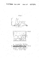
- FIG. 1 is a graph showing the color matching function of the XYZ colorimetric system
- FIG. 2 is a plan view showing an embodiment of the invention with interference filters and colored filters removed therefrom;
- FIG. 3 is a sectional view showing the embodiment of FIG. 2;
- FIG. 4 is a graph showing how the desired one of the transmission bands of an interference filter is selected by a colored filter
- FIG. 5 is a graph showing the selected transmission bands of the interference filters
- FIG. 6 is a graph showing spectral sensitivity curves each obtained from the combination of a photodiode, interference filter and colored filter when it is assumed that the spectral sensitivities of the photodiodes per se are constant;
- FIG. 7 is a graph showing how combined spectral sensitivities are obtained in a match with the color matching function
- FIG. 8 is a fragmentary enlarged view in section showing a modification wherein an interference filter is used as selecting means
- FIG. 9 is a plan view showing another embodiment wherein each of the photoelectric transducers comprises a multiplicity of photodiodes in a scattered arrangement
- FIG. 10 is an electric circuit diagram showing the connection of the photodiodes of the embodiment of FIG. 9;
- FIG. 11 is a plan view showing another embodiment including photoelectric transducers for measuring the intensity of incident light.
- FIG. 12 is a diagram showing the electric circuit of the embodiment of FIG. 11.
- FIG. 1 shows the color matching function of the CIE XYZ colorimetric system.
- the value x of the tristimulus values has two peaks at wavelengths of 600 nm and 440 nm, and y and z have peaks at 555 nm and 445 nm, respectively.
- the present invention provides a color sensing device having spectral sensitivity characteristics identical with the color matching function in the form of these curves.
- FIGS. 2 and 3 show the construction of the device.
- a thermally grown thin layer 2 of silicon dioxide is formed on an n-type silicon substrate 1, and four portions of the layer 2 are removed by etching to form windows.
- the substrate 1 is doped with p-type impurities, e.g. boron, by thermal diffusion through the windows to form p-type regions 3.
- the four p-n junction photodiodes 11, 12, 13 and 14 are formed on the silicon substrate 1.
- the light receiving faces of the photodiodes 11 to 14 are approximately in the ratio of 1.0:0.8:1.3:2.5 in area.
- Three bonding pads 21, 23 and 24 serving as positive electrodes are formed on the upper surface of the silicon substrate 1, while a common negative electrode 4 is provided over the entire bottom surface of the substrate 1.
- Electrodes are formed from aluminum or gold by vacuum evaporation or sputtering.
- the electrode 21, which is provided for the photodiodes 11 and 12 in common, is in ohmic contact with the p-type regions 3 thereof.
- the electrodes 23 and 24 are connected to the p-type regions of the photodiodes 13 and 14, respectively.
- Interference filters 31, 32, 33 and 34 are provided over the light receiving faces of the photodiodes 11, 12, 13 and 14, respectively.
- Each of the interference filters comprises a transparent dielectric layer 35, and light-transmitting metal films 36 and 37 sandwiching the layer 35 therebetween from above and below.
- Examples of useful dielectric materials are magnesium fluoride (MgF 2 ), zinc sulfide (ZnS), etc. Silver or aluminum is used for the metal films.
- the layer and films are formed by vacuum evaporation.
- the interference filters 31 to 34 differ in the thickness of the dielectric layer 35. The thickness is controlled by lift-off or like known technique. Sharp cutoff high-pass colored filters 41 to 44 are further formed over the interference filters 31 to 34, respectively.
- the filters 41 to 44 differ in cutoff wavelength.
- the colored filter can be produced, for example, by screenprinting a gelatin film colored with an organic pigment, by exposing a photosensitive film to light of the desired color, or by transfer technique.
- the interference filter has a plurality of transmission bands.
- the important characteristics of the transmission band are the center wavelength (peak wavelength) ⁇ m , half-width W and peak transmission ⁇ , which are given approximately by the following equations: ##EQU1## where m is the order of the transmission band and is given by a positive integer, t is the optical thickness of the dielectric layer involving the effect of phase change on internal reflection, ⁇ is the angle between the light which undergoes repeated internal reflection within the dielectric layer and a line normal to the surface of the dielectric layer, R is the reflectivity of the metal film, and A is the fraction of light absorbed by the metal film. Equation (1) shows that the peak wavelength ⁇ m is dependent on the thickness of the dielectric layer 35.
- the half-width W is dependent on the peak wavelength ⁇ m and on the reflectivity R of the metal films 36 and 37; the higher the reflectivity, the smaller is the half-width.
- the reflectivity of the metal films is dependent on the thickness thereof.
- FIG. 4 shows how one of the plurality of transmission bands of the interference filter is selected by the colored filter.
- Curve B shows the spectral transmittance of the colored filter 41.
- Indicated at C is the spectral transmittance curve afforded by the combination of the interference filter 31 and the colored filter 41. It will be understood that the desired one of the plurality of transmission bands of the interference filter 31 is selected by the colored filter 41. Similarly the colored filters 42 to 44 each select the desired one transmission band only for the interference filters 32 to 34.
- FIG. 5 shows the relative spectral transmittance curves D1 to D4 of the transmission bands thus selected for the interference filters 31 to 34.
- the peak transmissions of all the bands are equal.
- the peak wavelengths and half-widths of these transmission bands are given by Equations (1) and (2).
- Vacuum-evaporated aluminum films have higher adhesion to the substrate and undergo lesser variations in reflectivity with the lapse of time than silver films.
- the reflectivity of aluminum films increases at shorter wavelengths.
- the half-width of the transmission band of the interference filter decreases with an increase in the reflectivity of the metal film.
- the transmission bands D2 and D4 at shorter wavelengths are smaller in half-width than the bands D1 and D3 at longer wavelengths. This tendency is almost in agreement with the spectral reflectivity characteristics of aluminum films. Thus it is more advantageous to use aluminum films than silver films.
- FIG. 6 shows the transmittances D1 to D4 of FIG. 5 multiplied by the areas of the light receiving faces of the photodiodes 11 to 14, respectively, i.e. relative spectral sensitivity curves E1 to E4. It is herein assumed that the sensitivities of the photodiodes are constant on the wavelength axis.
- FIG. 7 shows curves F1 to F4 which represent curves E1 to E4 each multiplied by the spectral sensitivity G of the photodiode.
- the spectral sensitivities F1 to F4 thus obtained are true combined spectral sensitivities in proportion to the color matching function shown in FIG. 1.
- the peak sensitivities of the spectral sensitivities F1 to F4 are determined by the areas of the light receiving faces of the photodiodes 11 to 14.
- the peak values of the transmittances D1 to D4 (FIG. 5) afforded by the interference filters and the colored filters in combination are all assumed to be equal.
- Equation 3 indicates that the peak transmission of the interference filter is dependent on the reflectivity and the fraction of light absorbed by the metal film.
- the interference filters 31 to 34 differ from one another in the reflectivity of the metal films 36 and 37 and therefore in the peak transmission thereof.
- the areas of the light receiving faces of the photodiodes 31 to 34 are determined also in view of the differences in the peak transmission.
- the areas of the light receiving faces of the photodiodes 31 to 34 will be determined also in view of the spectral intensity of the light source.
- the output signal of the photodiode is given by the open-circuit voltage obtained when the circuit of its anode and cathode is opened, or by the short-circuit current obtained when the circuit is shorted.
- the short-circuit current is in proportion to the amount of incident light. It is now assumed that the sum of the short circuit currents of the photodiodes 31 and 32 from the electrode 21 is Ix, and the short circuit currents of the photodiodes 33 and 34 from the electrodes 23 and 24 are Iy and Iz, respectively.
- the chromaticity coordinates x and y are given by the following equations. ##EQU2## These coordinates x and y represent the nature of color other than lightness.
- the data relating to lightness is obtained from one or the sum of the short circuit currents Ix, Iy and Iz, or from the output of another photoelectric transducer provided separately.
- the circuit for calculating the chromaticity coordinates and the circuit for giving a color sensing signal output based on the result of calculation can be provided integrally on the semiconductor substrate 1.
- FIG. 8 shows a modification of the means for selecting the desired transmission band of the interference filter.
- Another interference filter 47 is formed by vacuum evaporation over the interference filter 31.
- the filter 47 comprises a dielectric layer 45, and metal films 46 and 36 sandwiching the layer 45 from above and below.
- One of the transmission bands of the interference filter 47 matches the transmission band of the filter 31 having a peak wavelength at 600 nm (although different in the order of band).
- FIGS. 9 and 10 show another embodiment, which comprises a large number of small p-n junction photodiodes arranged regularly in vertical and horizontal rows.
- the photodiodes 31e constituting a phototransducer 31 and the photodiodes 32e constituting a phototransducer 32 are in a scattered arrangement on a substrate 1 and are connected in parallel with an electrode 21 by an electroconductive pattern formed on the substrate 1.
- the peak value of spectral sensitivity F1 is determined by the sum of the areas of the light receiving faces of the photodiodes 31e, and the peak value of spectral sensitivity F2 by the corresponding sum of the photodiodes 32e.
- phototransducers 33 and 34 comprrise photodiodes 33e and 34e, respectively, in a dispersed arrangement.
- each phototransducer is thus composed of small photodiodes in a scattered arrangement, the measuring error that would result if the intensity of incident light varies from location to location can be minimized.
- FIGS. 11 and 12 show still another embodiment, which comprises photodiodes 11 and 12, 13, and 14 on a substrate 1 and photodiodes 51, 53 and 54 formed on the substrate 1 and positioned in the vicinity of the photodiodes 11 and 12, 13, and 14, respectively, for measuring the intensity of incident light.
- the diodes 51, 53 and 54 are connected to electrodes 61, 63 and 64, respectively, and are not provided with any interference or colored filter.
- the output signals from the photodiodes are fed to a compensation circuit 26 by way of amplifiers 25 or 65. Based on the output signals by the photodiodes 51, 53 and 54, the compensation circuit 26 detects whether or not the intensity of incident light differs at different positions and also detects the degree of the unevenness, if any. Based on the result, the circuit 26 corrects the output signals from the photodiodes 11 and 12, 13, and 14.
Abstract
Description
______________________________________
Transmission  Peak wavelength
                           Half-width
band          (nm)         (nm)
______________________________________
D1            600          80
D2            440          50
D3            555          100
D4            445          55
______________________________________
Claims (10)
Applications Claiming Priority (2)
| Application Number | Priority Date | Filing Date | Title |
|---|---|---|---|
| JP56-69838 | 1981-05-08 | ||
| JP56069838A JPS57184937A (en) | 1981-05-08 | 1981-05-08 | Color discriminating element |
Publications (1)
| Publication Number | Publication Date |
|---|---|
| US4547074A true US4547074A (en) | 1985-10-15 |
Family
ID=13414333
Family Applications (1)
| Application Number | Title | Priority Date | Filing Date |
|---|---|---|---|
| US06/376,138 Expired - Fee Related US4547074A (en) | 1981-05-08 | 1982-05-07 | Color sensing device |
Country Status (2)
| Country | Link |
|---|---|
| US (1) | US4547074A (en) |
| JP (1) | JPS57184937A (en) |
Cited By (57)
| Publication number | Priority date | Publication date | Assignee | Title |
|---|---|---|---|---|
| US4804833A (en) * | 1985-09-06 | 1989-02-14 | Minolta Camera Kabushiki Kaisha | Color sensing method and device therefor |
| US4822999A (en) * | 1986-05-01 | 1989-04-18 | Parr David T | Apparatus and method for detecting movement of an object |
| US4834541A (en) * | 1987-01-22 | 1989-05-30 | Agency Of Industrial Science & Technology | Color sensor |
| US4835384A (en) * | 1985-09-06 | 1989-05-30 | The University Of Liverpool | Device and method for determining displacement using colored transparent spheres |
| US4839685A (en) * | 1986-11-12 | 1989-06-13 | Fuji Photo Film Co., Ltd. | Light receiving element for a rangefinder |
| US4883952A (en) * | 1987-03-17 | 1989-11-28 | Jones Gordon R | Optical birefringment parameter measuring sensor |
| US4956555A (en) * | 1989-06-30 | 1990-09-11 | Rockwell International Corporation | Multicolor focal plane arrays |
| US4965449A (en) * | 1988-03-23 | 1990-10-23 | Canon Kabushiki Kaisha | Color information detecting device |
| US5020118A (en) * | 1984-06-13 | 1991-05-28 | Canon Kabushiki Kaisha | Image reading apparatus |
| US5050990A (en) * | 1990-08-24 | 1991-09-24 | Xerox Corporation | Variable detector geometry for resolving and sensing apparatus for filtering and other applications |
| US5087809A (en) * | 1990-11-26 | 1992-02-11 | Eastman Kodak Company | Spectrally selective dithering and color filter mask for increased image sensor blue sensitivity |
| US5128736A (en) * | 1988-01-12 | 1992-07-07 | Kanegafuchi Chemical Industry Co., Ltd. | Light sensitive semiconductor device |
| US5144498A (en) * | 1990-02-14 | 1992-09-01 | Hewlett-Packard Company | Variable wavelength light filter and sensor system |
| US5157465A (en) * | 1990-10-11 | 1992-10-20 | Kronberg James W | Universal fiber-optic C.I.E. colorimeter |
| EP0559138A1 (en) * | 1992-03-03 | 1993-09-08 | Canon Kabushiki Kaisha | Solid state image pick-up device |
| US5272518A (en) * | 1990-12-17 | 1993-12-21 | Hewlett-Packard Company | Colorimeter and calibration system |
| EP0650199A1 (en) * | 1993-10-22 | 1995-04-26 | Canon Kabushiki Kaisha | Filter for image sensor |
| US5726805A (en) * | 1996-06-25 | 1998-03-10 | Sandia Corporation | Optical filter including a sub-wavelength periodic structure and method of making |
| US5766006A (en) * | 1995-06-26 | 1998-06-16 | Murljacic; Maryann Lehmann | Tooth shade analyzer system and methods |
| US5789737A (en) * | 1997-01-22 | 1998-08-04 | Xerox Corporation | High dynamic range segmented pixel sensor array |
| US6076734A (en) * | 1997-10-07 | 2000-06-20 | Interval Research Corporation | Methods and systems for providing human/computer interfaces |
| US6078429A (en) * | 1998-07-22 | 2000-06-20 | Foveon, Inc. | Color separating prism having violet light component in red channel |
| US6164541A (en) * | 1997-10-10 | 2000-12-26 | Interval Research Group | Methods and systems for providing human/computer interfaces |
| US6210159B1 (en) | 1998-05-20 | 2001-04-03 | Shade Analyzing Technologies, Inc. | System and methods for analyzing tooth shades |
| US6256638B1 (en) | 1998-04-14 | 2001-07-03 | Interval Research Corporation | Printable interfaces and digital linkmarks |
| US20010056293A1 (en) * | 2000-05-10 | 2001-12-27 | George Brainard | Photoreceptor system for melatonin regulation and phototherapy |
| US6408331B1 (en) | 1995-07-27 | 2002-06-18 | Digimarc Corporation | Computer linking methods using encoded graphics |
| US6411725B1 (en) | 1995-07-27 | 2002-06-25 | Digimarc Corporation | Watermark enabled video objects |
| US20020195549A1 (en) * | 2001-06-12 | 2002-12-26 | Rafael Armament Development Authority Ltd. | Object detection method and system |
| US6575751B1 (en) | 1998-11-03 | 2003-06-10 | Shade Analyzing Technologies, Inc. | Interactive dental restorative network |
| US6580091B1 (en) * | 1996-11-08 | 2003-06-17 | Matsushita Electric Industrial Co., Ltd. | Apparatus and method for optical evaluation, apparatus and method for manufacturing semiconductor device, method of controlling apparatus for manufacturing semiconductor device, and semiconductor device |
| US6647130B2 (en) | 1993-11-18 | 2003-11-11 | Digimarc Corporation | Printable interfaces and digital linking with embedded codes |
| US6727108B2 (en) | 1996-11-08 | 2004-04-27 | Matsushita Electric Industrial Co., Ltd. | Apparatus and method for optical evaluation, apparatus and method for manufacturing semiconductor device, method of controlling apparatus for manufacturing semiconductor device, and semiconductor device |
| US6750971B2 (en) | 1999-12-08 | 2004-06-15 | X-Rite, Incorporated | Optical measurement device and related process |
| EP1471726A2 (en) * | 2003-04-22 | 2004-10-27 | Xerox Corporation | Image sensor array |
| US20050008190A1 (en) * | 1995-07-27 | 2005-01-13 | Levy Kenneth L. | Digital watermarking systems and methods |
| US20050074718A1 (en) * | 2003-10-03 | 2005-04-07 | Pye Graham | Tooth shade scan system and method |
| US20050112522A1 (en) * | 2003-11-26 | 2005-05-26 | Riley Mary F. | Method for selecting color for a dental prosthesis |
| US20050121599A1 (en) * | 2003-12-03 | 2005-06-09 | Chandra Mouli | Metal mesh filter-comprising semiconductor image sensor |
| US20050207044A1 (en) * | 2004-03-18 | 2005-09-22 | Oon Chin H | Color filter and method for fabricating the same |
| US20050205765A1 (en) * | 2004-03-18 | 2005-09-22 | Tan Boon K | Color photodetector array |
| DE10018444B4 (en) * | 1999-05-04 | 2006-01-26 | Soft Imaging System Gmbh | Semiconductor system for registering spectra, color signals, color images and the like |
| US20060103864A1 (en) * | 2004-11-16 | 2006-05-18 | Datacolor Holding Ag | Method for designing a colorimeter having integral CIE color-matching filters |
| US20060119849A1 (en) * | 2004-11-17 | 2006-06-08 | Brian Levey | Tristimulus colorimeter having integral dye filters |
| US7111168B2 (en) | 2000-05-01 | 2006-09-19 | Digimarc Corporation | Digital watermarking systems |
| US20060215193A1 (en) * | 2005-03-23 | 2006-09-28 | Colman Shannon | Method for designing a colorimeter having illuminant-weighted CIE color-matching filters |
| US20060215162A1 (en) * | 2005-03-23 | 2006-09-28 | Colman Shannon | Reflectance sensor for integral illuminant-weighted CIE color matching filters |
| US7118374B2 (en) | 2003-06-09 | 2006-10-10 | Ivoclar Vivadent Ag | Enhanced tooth shade guide |
| US20070026363A1 (en) * | 1998-11-03 | 2007-02-01 | Maryann Lehmann | Interactive dental restorative network |
| US20100208266A1 (en) * | 2009-02-17 | 2010-08-19 | Colman Shannon | Tristimulus colorimeter having integral dye filters |
| FR2966977A1 (en) * | 2010-11-03 | 2012-05-04 | Commissariat Energie Atomique | VISIBLE AND NEAR INFRARED RADIATION DETECTOR |
| US20140375994A1 (en) * | 2013-06-19 | 2014-12-25 | Yuji Yamanaka | Measuring apparatus, measuring system, and measuring method |
| EP3187909A1 (en) * | 2015-12-29 | 2017-07-05 | Viavi Solutions Inc. | Metal mirror based multispectral filter array |
| USRE46557E1 (en) * | 2001-01-09 | 2017-09-19 | Sony Semiconductor Solutions Corporation | Image processing apparatus and method for generating a restoration image |
| WO2018007368A1 (en) * | 2016-07-05 | 2018-01-11 | Idt Europe Gmbh | Color sensor and method of its production |
| US9880057B2 (en) | 2010-11-03 | 2018-01-30 | Commissariat à l'Energie Atomique et aux Energies Alternatives | Visible and near-infrared radiation detector |
| US11450698B2 (en) | 2015-12-29 | 2022-09-20 | Viavi Solutions Inc. | Dielectric mirror based multispectral filter array |
Families Citing this family (4)
| Publication number | Priority date | Publication date | Assignee | Title |
|---|---|---|---|---|
| JPS60262032A (en) * | 1984-06-09 | 1985-12-25 | Mazda Motor Corp | Color discrimination apparatus |
| JPH0672806B2 (en) * | 1985-03-25 | 1994-09-14 | 山武ハネウエル株式会社 | Color measurement method |
| WO2004076997A1 (en) | 2003-02-28 | 2004-09-10 | Hamamatsu Photonics K.K. | Spectroscope |
| WO2009102323A1 (en) | 2008-02-12 | 2009-08-20 | Hewlett-Packard Development Company, L.P. | Color detector |
Citations (6)
| Publication number | Priority date | Publication date | Assignee | Title |
|---|---|---|---|---|
| US3389265A (en) * | 1965-05-03 | 1968-06-18 | Du Pont | Colorimeter for measuring the tristimulus coefficients of color in a laterally moving material |
| DE2424545A1 (en) * | 1973-05-28 | 1975-01-02 | Magyar Tudomanyos Akademia | DEVICE FOR DETERMINING THE COLOR COMPONENTS AND THE COLOR COORDINATES |
| US3929398A (en) * | 1971-08-18 | 1975-12-30 | Harry E Bates | High speed optical wavelength detection system |
| US3985449A (en) * | 1975-02-07 | 1976-10-12 | International Business Machines Corporation | Semiconductor color detector |
| DE2546253A1 (en) * | 1975-10-13 | 1977-04-14 | Optronik Gmbh | Spectral analyzer and colorimeter photo: receiver - has several light sensitive receivers with differing spectral sensitivities covered with block filter(s) |
| JPS54154348A (en) * | 1978-05-25 | 1979-12-05 | Canon Inc | Color image reader |
Family Cites Families (2)
| Publication number | Priority date | Publication date | Assignee | Title |
|---|---|---|---|---|
| JPS4833877A (en) * | 1971-09-01 | 1973-05-14 | ||
| JPS5853854B2 (en) * | 1975-06-10 | 1983-12-01 | 株式会社東芝 | Shikichiyoukenshiyutsusouchi |
-
1981
- 1981-05-08 JP JP56069838A patent/JPS57184937A/en active Pending
-
1982
- 1982-05-07 US US06/376,138 patent/US4547074A/en not_active Expired - Fee Related
Patent Citations (6)
| Publication number | Priority date | Publication date | Assignee | Title |
|---|---|---|---|---|
| US3389265A (en) * | 1965-05-03 | 1968-06-18 | Du Pont | Colorimeter for measuring the tristimulus coefficients of color in a laterally moving material |
| US3929398A (en) * | 1971-08-18 | 1975-12-30 | Harry E Bates | High speed optical wavelength detection system |
| DE2424545A1 (en) * | 1973-05-28 | 1975-01-02 | Magyar Tudomanyos Akademia | DEVICE FOR DETERMINING THE COLOR COMPONENTS AND THE COLOR COORDINATES |
| US3985449A (en) * | 1975-02-07 | 1976-10-12 | International Business Machines Corporation | Semiconductor color detector |
| DE2546253A1 (en) * | 1975-10-13 | 1977-04-14 | Optronik Gmbh | Spectral analyzer and colorimeter photo: receiver - has several light sensitive receivers with differing spectral sensitivities covered with block filter(s) |
| JPS54154348A (en) * | 1978-05-25 | 1979-12-05 | Canon Inc | Color image reader |
Non-Patent Citations (2)
| Title |
|---|
| Kato et al., Journal of Physics E, vol. 9, No. 12, Dec. 1976, pp. 1070 1072. * |
| Kato et al., Journal of Physics E, vol. 9, No. 12, Dec. 1976, pp. 1070-1072. |
Cited By (121)
| Publication number | Priority date | Publication date | Assignee | Title |
|---|---|---|---|---|
| US5020118A (en) * | 1984-06-13 | 1991-05-28 | Canon Kabushiki Kaisha | Image reading apparatus |
| US4835384A (en) * | 1985-09-06 | 1989-05-30 | The University Of Liverpool | Device and method for determining displacement using colored transparent spheres |
| US4891510A (en) * | 1985-09-06 | 1990-01-02 | The University Of Liverpool | Device and method for determining displacement |
| US4891509A (en) * | 1985-09-06 | 1990-01-02 | The University Of Liverpool | Device and method for determining displacement |
| US4804833A (en) * | 1985-09-06 | 1989-02-14 | Minolta Camera Kabushiki Kaisha | Color sensing method and device therefor |
| US4822999A (en) * | 1986-05-01 | 1989-04-18 | Parr David T | Apparatus and method for detecting movement of an object |
| US4839685A (en) * | 1986-11-12 | 1989-06-13 | Fuji Photo Film Co., Ltd. | Light receiving element for a rangefinder |
| US4834541A (en) * | 1987-01-22 | 1989-05-30 | Agency Of Industrial Science & Technology | Color sensor |
| US4883952A (en) * | 1987-03-17 | 1989-11-28 | Jones Gordon R | Optical birefringment parameter measuring sensor |
| US5128736A (en) * | 1988-01-12 | 1992-07-07 | Kanegafuchi Chemical Industry Co., Ltd. | Light sensitive semiconductor device |
| US4965449A (en) * | 1988-03-23 | 1990-10-23 | Canon Kabushiki Kaisha | Color information detecting device |
| US4956555A (en) * | 1989-06-30 | 1990-09-11 | Rockwell International Corporation | Multicolor focal plane arrays |
| US5144498A (en) * | 1990-02-14 | 1992-09-01 | Hewlett-Packard Company | Variable wavelength light filter and sensor system |
| US5050990A (en) * | 1990-08-24 | 1991-09-24 | Xerox Corporation | Variable detector geometry for resolving and sensing apparatus for filtering and other applications |
| US5157465A (en) * | 1990-10-11 | 1992-10-20 | Kronberg James W | Universal fiber-optic C.I.E. colorimeter |
| US5087809A (en) * | 1990-11-26 | 1992-02-11 | Eastman Kodak Company | Spectrally selective dithering and color filter mask for increased image sensor blue sensitivity |
| US5272518A (en) * | 1990-12-17 | 1993-12-21 | Hewlett-Packard Company | Colorimeter and calibration system |
| EP0559138A1 (en) * | 1992-03-03 | 1993-09-08 | Canon Kabushiki Kaisha | Solid state image pick-up device |
| EP0693786A3 (en) * | 1992-03-03 | 1996-02-28 | Canon Kk | Solid state image pick-up device |
| US5506430A (en) * | 1992-03-03 | 1996-04-09 | Canon Kabushiki Kaisha | Solid state image pick-up device with differing capacitances |
| EP0650199A1 (en) * | 1993-10-22 | 1995-04-26 | Canon Kabushiki Kaisha | Filter for image sensor |
| US5648653A (en) * | 1993-10-22 | 1997-07-15 | Canon Kabushiki Kaisha | Optical filter having alternately laminated thin layers provided on a light receiving surface of an image sensor |
| US6647130B2 (en) | 1993-11-18 | 2003-11-11 | Digimarc Corporation | Printable interfaces and digital linking with embedded codes |
| US20050118549A1 (en) * | 1995-06-26 | 2005-06-02 | Shade Analyzing Technologies, Inc. | Tooth shade analyzer system and methods |
| US5766006A (en) * | 1995-06-26 | 1998-06-16 | Murljacic; Maryann Lehmann | Tooth shade analyzer system and methods |
| US5961324A (en) * | 1995-06-26 | 1999-10-05 | Shade Analyzing Technologies, Inc. | Tooth shade analyzer system and methods |
| US6358047B2 (en) | 1995-06-26 | 2002-03-19 | Shade Analyzing Technologies, Inc. | Tooth shade analyzer system and methods |
| US7946845B2 (en) | 1995-06-26 | 2011-05-24 | Shade Analyzing Technologies, Inc. | Tooth shade analyzer system and methods |
| US6832913B2 (en) | 1995-06-26 | 2004-12-21 | Shade Analyzing Technologies, Inc. | Tooth shade analyzer system and methods |
| US20110188086A1 (en) * | 1995-06-26 | 2011-08-04 | Shade Analyzing Technologies, Inc. | Tooth shade analyzer system and methods |
| US7393209B2 (en) | 1995-06-26 | 2008-07-01 | Shade Analyzing Technologies, Inc. | Tooth shade analyzer system and methods |
| US6305933B1 (en) | 1995-06-26 | 2001-10-23 | Shade Analyzing Technologies, Inc. | Tooth shade analyzer system and methods |
| US6408331B1 (en) | 1995-07-27 | 2002-06-18 | Digimarc Corporation | Computer linking methods using encoded graphics |
| US7436976B2 (en) | 1995-07-27 | 2008-10-14 | Digimarc Corporation | Digital watermarking systems and methods |
| US7050603B2 (en) | 1995-07-27 | 2006-05-23 | Digimarc Corporation | Watermark encoded video, and related methods |
| US6411725B1 (en) | 1995-07-27 | 2002-06-25 | Digimarc Corporation | Watermark enabled video objects |
| US20050008190A1 (en) * | 1995-07-27 | 2005-01-13 | Levy Kenneth L. | Digital watermarking systems and methods |
| US5726805A (en) * | 1996-06-25 | 1998-03-10 | Sandia Corporation | Optical filter including a sub-wavelength periodic structure and method of making |
| US6849470B1 (en) | 1996-11-08 | 2005-02-01 | Matsushita Electric Industrial Co., Ltd. | Apparatus and method for optical evaluation, apparatus and method for manufacturing semiconductor device, method of controlling apparatus for manufacturing semiconductor device, and semiconductor device |
| US6727108B2 (en) | 1996-11-08 | 2004-04-27 | Matsushita Electric Industrial Co., Ltd. | Apparatus and method for optical evaluation, apparatus and method for manufacturing semiconductor device, method of controlling apparatus for manufacturing semiconductor device, and semiconductor device |
| US6580091B1 (en) * | 1996-11-08 | 2003-06-17 | Matsushita Electric Industrial Co., Ltd. | Apparatus and method for optical evaluation, apparatus and method for manufacturing semiconductor device, method of controlling apparatus for manufacturing semiconductor device, and semiconductor device |
| US5789737A (en) * | 1997-01-22 | 1998-08-04 | Xerox Corporation | High dynamic range segmented pixel sensor array |
| US6540141B1 (en) | 1997-10-07 | 2003-04-01 | Interval Research Corporation | Methods and systems for providing human/computer interfaces |
| US6587859B2 (en) | 1997-10-07 | 2003-07-01 | Interval Research Corporation | Printable interfaces and digital linkmarks |
| US6518950B1 (en) | 1997-10-07 | 2003-02-11 | Interval Research Corporation | Methods and systems for providing human/computer interfaces |
| US6989816B1 (en) | 1997-10-07 | 2006-01-24 | Vulcan Patents Llc | Methods and systems for providing human/computer interfaces |
| US6076734A (en) * | 1997-10-07 | 2000-06-20 | Interval Research Corporation | Methods and systems for providing human/computer interfaces |
| US6439459B1 (en) | 1997-10-07 | 2002-08-27 | Interval Research Corporation | Methods and systems for providing human/computer interfaces |
| US6164541A (en) * | 1997-10-10 | 2000-12-26 | Interval Research Group | Methods and systems for providing human/computer interfaces |
| US6256638B1 (en) | 1998-04-14 | 2001-07-03 | Interval Research Corporation | Printable interfaces and digital linkmarks |
| US6210159B1 (en) | 1998-05-20 | 2001-04-03 | Shade Analyzing Technologies, Inc. | System and methods for analyzing tooth shades |
| US6078429A (en) * | 1998-07-22 | 2000-06-20 | Foveon, Inc. | Color separating prism having violet light component in red channel |
| US6575751B1 (en) | 1998-11-03 | 2003-06-10 | Shade Analyzing Technologies, Inc. | Interactive dental restorative network |
| US20070026363A1 (en) * | 1998-11-03 | 2007-02-01 | Maryann Lehmann | Interactive dental restorative network |
| US8105084B2 (en) | 1998-11-03 | 2012-01-31 | Shade Analyzing Technologies, Inc. | Interactive dental restorative network |
| US6786726B2 (en) | 1998-11-03 | 2004-09-07 | Shade Analyzing Technologies, Inc. | Interactive dental restorative network |
| US8790118B2 (en) | 1998-11-03 | 2014-07-29 | Shade Analyzing Technologies, Inc. | Interactive dental restorative network |
| EP2133820A2 (en) | 1998-11-03 | 2009-12-16 | Shade Analyzing Technologies, Inc. | System and methods for analyzing tooth shades |
| US8851893B2 (en) | 1998-11-03 | 2014-10-07 | Shade Analyzing Technologies, Inc. | Interactive dental restorative network |
| US7581953B2 (en) | 1998-11-03 | 2009-09-01 | Shade Analyzing Technologies, Inc. | Interactive dental restorative network |
| US20050003329A1 (en) * | 1998-11-03 | 2005-01-06 | Shade Analyzing Technologies, Inc. | Interactive dental restorative network |
| DE10018444B4 (en) * | 1999-05-04 | 2006-01-26 | Soft Imaging System Gmbh | Semiconductor system for registering spectra, color signals, color images and the like |
| US20050122518A1 (en) * | 1999-12-08 | 2005-06-09 | Overbeck James L. | Optical measurement device and related process |
| US6867864B2 (en) | 1999-12-08 | 2005-03-15 | X-Rite, Incorporated | Optical measurement device and related process |
| US6750971B2 (en) | 1999-12-08 | 2004-06-15 | X-Rite, Incorporated | Optical measurement device and related process |
| US7030986B2 (en) | 1999-12-08 | 2006-04-18 | X-Rite Incorporated | Optical measurement device and related process |
| US7050168B2 (en) | 1999-12-08 | 2006-05-23 | X-Rite, Incorporated | Optical measurement device and related process |
| US7111168B2 (en) | 2000-05-01 | 2006-09-19 | Digimarc Corporation | Digital watermarking systems |
| US7678140B2 (en) * | 2000-05-10 | 2010-03-16 | George Brainard | Photoreceptor system for melatonin regulation and phototherapy |
| US8366755B2 (en) | 2000-05-10 | 2013-02-05 | Progressive Lighting And Radiometrics, Llc | Photoreceptor system for melatonin regulation and phototherapy |
| US10603507B2 (en) | 2000-05-10 | 2020-03-31 | Progressive Lighting And Radiometrics, Llc. | Method and apparatus for determining circadian input |
| US10213619B2 (en) | 2000-05-10 | 2019-02-26 | Progressive Lighting And Radiometrics, Llc | Method and apparatus for determining circadian input |
| US20100214559A1 (en) * | 2000-05-10 | 2010-08-26 | George Brainard | Photoreceptor system for melatonin regulation and phototherapy |
| US20010056293A1 (en) * | 2000-05-10 | 2001-12-27 | George Brainard | Photoreceptor system for melatonin regulation and phototherapy |
| USRE47062E1 (en) | 2001-01-09 | 2018-09-25 | Sony Semiconductor Solutions Corporation | Image processing apparatus and method for generating a restoration image |
| USRE46557E1 (en) * | 2001-01-09 | 2017-09-19 | Sony Semiconductor Solutions Corporation | Image processing apparatus and method for generating a restoration image |
| US20060006314A1 (en) * | 2001-06-12 | 2006-01-12 | Rafael Armament Development Authority Ltd. | Object detection method and system |
| US7154085B2 (en) | 2001-06-12 | 2006-12-26 | Rafael Armament Development Authority, Ltd. | Object detection method and system |
| US6943337B2 (en) * | 2001-06-12 | 2005-09-13 | Rafael Armament Development Authority Ltd. | Object detection method and system |
| US20020195549A1 (en) * | 2001-06-12 | 2002-12-26 | Rafael Armament Development Authority Ltd. | Object detection method and system |
| US7446907B2 (en) * | 2003-04-22 | 2008-11-04 | Xerox Corporation | Photosensor architecture for a color raster input scanner |
| EP1471726A2 (en) * | 2003-04-22 | 2004-10-27 | Xerox Corporation | Image sensor array |
| US20040212858A1 (en) * | 2003-04-22 | 2004-10-28 | Xerox Corporation. | Photosensor architecture for a color raster input scanner |
| EP1471726A3 (en) * | 2003-04-22 | 2005-06-15 | Xerox Corporation | Image sensor array |
| US7118374B2 (en) | 2003-06-09 | 2006-10-10 | Ivoclar Vivadent Ag | Enhanced tooth shade guide |
| US7341450B2 (en) | 2003-10-03 | 2008-03-11 | Shade Analyzing Technologies, Inc. | Tooth shade scan system and method |
| US20050074718A1 (en) * | 2003-10-03 | 2005-04-07 | Pye Graham | Tooth shade scan system and method |
| US20050112522A1 (en) * | 2003-11-26 | 2005-05-26 | Riley Mary F. | Method for selecting color for a dental prosthesis |
| US7223960B2 (en) * | 2003-12-03 | 2007-05-29 | Micron Technology, Inc. | Image sensor, an image sensor pixel, and methods of forming the same |
| US20050121599A1 (en) * | 2003-12-03 | 2005-06-09 | Chandra Mouli | Metal mesh filter-comprising semiconductor image sensor |
| US20050207044A1 (en) * | 2004-03-18 | 2005-09-22 | Oon Chin H | Color filter and method for fabricating the same |
| CN1670493B (en) * | 2004-03-18 | 2010-12-22 | 安华高科技Ecbuip(新加坡)私人有限公司 | Improved color photodetector array |
| US7285768B2 (en) * | 2004-03-18 | 2007-10-23 | Avago Technologies Ecbu Ip (Singapore) Pte Ltd | Color photodetector array |
| US20050205765A1 (en) * | 2004-03-18 | 2005-09-22 | Tan Boon K | Color photodetector array |
| US7420680B2 (en) | 2004-11-16 | 2008-09-02 | Datacolor Holding Ag | Method for designing a colorimeter having integral CIE color-matching filters |
| US20060103864A1 (en) * | 2004-11-16 | 2006-05-18 | Datacolor Holding Ag | Method for designing a colorimeter having integral CIE color-matching filters |
| US7593105B2 (en) | 2004-11-17 | 2009-09-22 | Datacolor Holding Ag | Tristimulus colorimeter having integral dye filters |
| EP1812781A4 (en) * | 2004-11-17 | 2010-04-07 | Datacolor Holding Ag | Tristimulus colorimeter having integral dye filters |
| US20060119849A1 (en) * | 2004-11-17 | 2006-06-08 | Brian Levey | Tristimulus colorimeter having integral dye filters |
| EP1812781A2 (en) * | 2004-11-17 | 2007-08-01 | Datacolor Holding Ag | Tristimulus colorimeter having integral dye filters |
| US7580130B2 (en) | 2005-03-23 | 2009-08-25 | Datacolor Holding Ag | Method for designing a colorimeter having integral illuminant-weighted CIE color-matching filters |
| US7474402B2 (en) * | 2005-03-23 | 2009-01-06 | Datacolor Holding Ag | Reflectance sensor for integral illuminant-weighted CIE color matching filters |
| US20060215193A1 (en) * | 2005-03-23 | 2006-09-28 | Colman Shannon | Method for designing a colorimeter having illuminant-weighted CIE color-matching filters |
| US20060215162A1 (en) * | 2005-03-23 | 2006-09-28 | Colman Shannon | Reflectance sensor for integral illuminant-weighted CIE color matching filters |
| US20100208266A1 (en) * | 2009-02-17 | 2010-08-19 | Colman Shannon | Tristimulus colorimeter having integral dye filters |
| FR2966977A1 (en) * | 2010-11-03 | 2012-05-04 | Commissariat Energie Atomique | VISIBLE AND NEAR INFRARED RADIATION DETECTOR |
| US9880057B2 (en) | 2010-11-03 | 2018-01-30 | Commissariat à l'Energie Atomique et aux Energies Alternatives | Visible and near-infrared radiation detector |
| WO2012059657A1 (en) * | 2010-11-03 | 2012-05-10 | Commissariat A L Energie Atomique Et Aux Energies Alternatives | Detector of visible and near-infrared radiation |
| US9040916B2 (en) * | 2010-11-03 | 2015-05-26 | Commissariat A L'energie Atomique Et Aux Energies Alternatives | Visible and near-infrared radiation detector |
| US20130214160A1 (en) * | 2010-11-03 | 2013-08-22 | Commissariat A L'energie Atomique Et Aux Energies Alternatives | Visible and near-infrared radiation detector |
| US20140375994A1 (en) * | 2013-06-19 | 2014-12-25 | Yuji Yamanaka | Measuring apparatus, measuring system, and measuring method |
| US9638575B2 (en) * | 2013-06-19 | 2017-05-02 | Ricoh Company, Ltd. | Measuring apparatus, measuring system, and measuring method |
| US9923007B2 (en) | 2015-12-29 | 2018-03-20 | Viavi Solutions Inc. | Metal mirror based multispectral filter array |
| EP3187909A1 (en) * | 2015-12-29 | 2017-07-05 | Viavi Solutions Inc. | Metal mirror based multispectral filter array |
| US10651216B2 (en) | 2015-12-29 | 2020-05-12 | Viavi Solutions Inc. | Metal mirror based multispectral filter array |
| US11114485B2 (en) | 2015-12-29 | 2021-09-07 | Viavi Solutions Inc. | Metal mirror based multispectral filter array |
| US11450698B2 (en) | 2015-12-29 | 2022-09-20 | Viavi Solutions Inc. | Dielectric mirror based multispectral filter array |
| US11670658B2 (en) | 2015-12-29 | 2023-06-06 | Viavi Solutions Inc. | Metal mirror based multispectral filter array |
| WO2018007368A1 (en) * | 2016-07-05 | 2018-01-11 | Idt Europe Gmbh | Color sensor and method of its production |
| US20190170584A1 (en) * | 2016-07-05 | 2019-06-06 | Integrated Device Technology, Inc. | Color sensor and method of its production |
| US10816403B2 (en) | 2016-07-05 | 2020-10-27 | Integrated Device Technology, Inc. | Color sensor and method of its production |
Also Published As
| Publication number | Publication date |
|---|---|
| JPS57184937A (en) | 1982-11-13 |
Similar Documents
| Publication | Publication Date | Title |
|---|---|---|
| US4547074A (en) | Color sensing device | |
| CN101611626B (en) | Ambient light detectors using conventional cmos image sensor process | |
| US4822998A (en) | Spectral sensor with interference filter | |
| US5020910A (en) | Monolithic diffraction spectrometer | |
| US5144498A (en) | Variable wavelength light filter and sensor system | |
| US7916301B2 (en) | Filter design for colorimetric measurement | |
| US4820915A (en) | Color sensor with amorphous pin structure | |
| US20240047494A1 (en) | Micro spectrum chip based on units of random shapes | |
| US4776702A (en) | Device for color distinction | |
| CA2036114C (en) | Spectral resolving and sensing apparatus | |
| US4804833A (en) | Color sensing method and device therefor | |
| JP2011511946A (en) | COLOR DETECTOR HAVING OPTICAL DETECTOR WITH ENLARGED AREA | |
| Knipp et al. | Stacked amorphous silicon color sensors | |
| US3987298A (en) | Photodetector system for determination of the wavelength of incident radiation | |
| US20220344381A1 (en) | Micro spectrum chip based on units of different shapes | |
| Herzog et al. | Characterization of novel three-and six-channel color moire free sensors | |
| DE3217227C2 (en) | Color detection device | |
| Chouikha et al. | Colour detection using buried triple pn junction structure implemented in BiCMOS process | |
| JPH03202732A (en) | Color sensor | |
| JPS623628A (en) | Color discriminating device | |
| Kato et al. | Integrated transducer for color distinction | |
| JPS61277024A (en) | Light spectrum detector | |
| US5103100A (en) | X-ray detector | |
| JPH025393Y2 (en) | ||
| US5327005A (en) | Striped contact IR detector |
Legal Events
| Date | Code | Title | Description |
|---|---|---|---|
| AS | Assignment |
Owner name: OMRON TATEISI ELECTRONICS CO. 10 TSUCHIDO-CHO, HAN Free format text: ASSIGNMENT OF ASSIGNORS INTEREST.;ASSIGNORS:HINODA, SEISUKE;HIRANO, MASAO;KATO, MITSUTAKA;AND OTHERS;REEL/FRAME:003994/0681 Effective date: 19820430 |
|
| FEPP | Fee payment procedure |
Free format text: PAYOR NUMBER ASSIGNED (ORIGINAL EVENT CODE: ASPN); ENTITY STATUS OF PATENT OWNER: LARGE ENTITY |
|
| FPAY | Fee payment |
Year of fee payment: 4 |
|
| REMI | Maintenance fee reminder mailed | ||
| LAPS | Lapse for failure to pay maintenance fees | ||
| FP | Lapsed due to failure to pay maintenance fee |
Effective date: 19891017 |
|
| STCH | Information on status: patent discontinuation |
Free format text: PATENT EXPIRED DUE TO NONPAYMENT OF MAINTENANCE FEES UNDER 37 CFR 1.362 |