US4550239A - Automatic plasma processing device and heat treatment device - Google Patents
Automatic plasma processing device and heat treatment device Download PDFInfo
- Publication number
- US4550239A US4550239A US06/424,503 US42450382A US4550239A US 4550239 A US4550239 A US 4550239A US 42450382 A US42450382 A US 42450382A US 4550239 A US4550239 A US 4550239A
- Authority
- US
- United States
- Prior art keywords
- wafers
- automatic
- holding member
- plasma
- plasma processing
- Prior art date
- Legal status (The legal status is an assumption and is not a legal conclusion. Google has not performed a legal analysis and makes no representation as to the accuracy of the status listed.)
- Expired - Lifetime
Links
Images


Classifications
-
- H—ELECTRICITY
- H01—ELECTRIC ELEMENTS
- H01L—SEMICONDUCTOR DEVICES NOT COVERED BY CLASS H10
- H01L21/00—Processes or apparatus adapted for the manufacture or treatment of semiconductor or solid state devices or of parts thereof
- H01L21/67—Apparatus specially adapted for handling semiconductor or electric solid state devices during manufacture or treatment thereof; Apparatus specially adapted for handling wafers during manufacture or treatment of semiconductor or electric solid state devices or components ; Apparatus not specifically provided for elsewhere
- H01L21/677—Apparatus specially adapted for handling semiconductor or electric solid state devices during manufacture or treatment thereof; Apparatus specially adapted for handling wafers during manufacture or treatment of semiconductor or electric solid state devices or components ; Apparatus not specifically provided for elsewhere for conveying, e.g. between different workstations
- H01L21/67763—Apparatus specially adapted for handling semiconductor or electric solid state devices during manufacture or treatment thereof; Apparatus specially adapted for handling wafers during manufacture or treatment of semiconductor or electric solid state devices or components ; Apparatus not specifically provided for elsewhere for conveying, e.g. between different workstations the wafers being stored in a carrier, involving loading and unloading
- H01L21/67778—Apparatus specially adapted for handling semiconductor or electric solid state devices during manufacture or treatment thereof; Apparatus specially adapted for handling wafers during manufacture or treatment of semiconductor or electric solid state devices or components ; Apparatus not specifically provided for elsewhere for conveying, e.g. between different workstations the wafers being stored in a carrier, involving loading and unloading involving loading and unloading of wafers
- H01L21/67781—Batch transfer of wafers
-
- Y—GENERAL TAGGING OF NEW TECHNOLOGICAL DEVELOPMENTS; GENERAL TAGGING OF CROSS-SECTIONAL TECHNOLOGIES SPANNING OVER SEVERAL SECTIONS OF THE IPC; TECHNICAL SUBJECTS COVERED BY FORMER USPC CROSS-REFERENCE ART COLLECTIONS [XRACs] AND DIGESTS
- Y10—TECHNICAL SUBJECTS COVERED BY FORMER USPC
- Y10S—TECHNICAL SUBJECTS COVERED BY FORMER USPC CROSS-REFERENCE ART COLLECTIONS [XRACs] AND DIGESTS
- Y10S156/00—Adhesive bonding and miscellaneous chemical manufacture
- Y10S156/912—Differential etching apparatus having a vertical tube reactor
-
- Y—GENERAL TAGGING OF NEW TECHNOLOGICAL DEVELOPMENTS; GENERAL TAGGING OF CROSS-SECTIONAL TECHNOLOGIES SPANNING OVER SEVERAL SECTIONS OF THE IPC; TECHNICAL SUBJECTS COVERED BY FORMER USPC CROSS-REFERENCE ART COLLECTIONS [XRACs] AND DIGESTS
- Y10—TECHNICAL SUBJECTS COVERED BY FORMER USPC
- Y10S—TECHNICAL SUBJECTS COVERED BY FORMER USPC CROSS-REFERENCE ART COLLECTIONS [XRACs] AND DIGESTS
- Y10S414/00—Material or article handling
- Y10S414/135—Associated with semiconductor wafer handling
- Y10S414/137—Associated with semiconductor wafer handling including means for charging or discharging wafer cassette
-
- Y—GENERAL TAGGING OF NEW TECHNOLOGICAL DEVELOPMENTS; GENERAL TAGGING OF CROSS-SECTIONAL TECHNOLOGIES SPANNING OVER SEVERAL SECTIONS OF THE IPC; TECHNICAL SUBJECTS COVERED BY FORMER USPC CROSS-REFERENCE ART COLLECTIONS [XRACs] AND DIGESTS
- Y10—TECHNICAL SUBJECTS COVERED BY FORMER USPC
- Y10S—TECHNICAL SUBJECTS COVERED BY FORMER USPC CROSS-REFERENCE ART COLLECTIONS [XRACs] AND DIGESTS
- Y10S414/00—Material or article handling
- Y10S414/135—Associated with semiconductor wafer handling
- Y10S414/14—Wafer cassette transporting
Definitions
- the present invention relates generally to an automatic plasma processing device. More particularly, the invention relates to a vertical automatic plasma processing device having a vertically disposed plasma generating chamber which is employed for etching and cleaning of semiconductor wafers as intermediate products during production of chips having large scale integrated circuits such as LSI's and VLSI's formed thereon, for ashing of photoresist layers on surfaces of such wafers, etc.
- production of chips having a large scale integrated circuit such as an LSI formed thereon necessarily includes a process of etching an insulator film, a semiconductor film or a metal film through a photoresist film having a fine pattern formed on a semiconductor wafer, another process of cleaning such films, and a process of ashing to remove the remaining photoresist film used for the etching from the surface of the wafer.
- the aforesaid processes are effected by a wet type processing in which various liquid chemicals such as inorganic acids, organic solvents, etc., are employed.
- various liquid chemicals such as inorganic acids, organic solvents, etc.
- the present invention effectively overcomes the foregoing problems attendant conventional techniques as described hereinabove.
- the present invention provides an automatic plasma processing device, comprising: at least one cassette member adapted to contain a plurality of semiconductor wafers therein; a feeding mechanism for taking out the wafers one by one from the cassette member and for feeding the same; a holding member operable for receiving the wafers one by one from the feeding mechanism and for holding a plurality of such wafers therein; a driving mechanism for driving the holding member to move in a substantially vertical direction; a plasma chamber disposed in a substantially vertical direction such that the holding member may be moved in the vertical direction into and out of the plasma chamber; a plasma generating mechanism for generating plasma in the plasma chamber in order to effect plasma processing of the wafers with the plasma thus generated; and a control system for controlling the feeding mechanism, the driving mechanism and the plasma generating mechanism in accordance with a predetermined sequence.
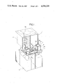
- FIG. 1 is a general perspective view of an automatic plasma processing device according to the present invention.
- FIG. 2 is a perspective view showing an inside structure of the device of FIG. 1.
- FIG. 3 is a side elevational view showing part of a wafer container cassette.
- FIG. 4 is a front elevational view showing an essential part of a wafer feeding mechanism.
- an automatic heat treatment or plasma processing device which includes a body 1 substantially in the form of a box.
- the device body 1 has a substantially cylindrical treatment chamber or plasma generating chamber 2 made of quartz disposed therein in a substantially vertical direction or in a direction in which it has a substantially vertical axis.
- the chamber 2 is closed at the top end 2a thereof and is open at the lower end 2b thereof (i.e., it is downwardly opening) in order to allow semiconductor wafers 3 to be loaded into and unloaded from the chamber 2 through the opening.
- a plasma generating and heating mechanism including an electrode plate (not shown) and a heating coil 2c, such as a high-frequency inductive heating coil is provided around an outer periphery of the chamber 2 and a high frequency voltage is applied thereto from a high frequency power source 4 provided in the body 1.
- a resistance heating coil or a heating lamp can alternatively be employed as a heating means.
- the device body 1 has an extruding portion or apron 5 provided at a front lower half portion thereof.
- Several operating buttons 7 are disposed on an upper wall of the apron 5 and a pair of container cassettes 8 adapted to contain therein a plurality of sheet-like treatment objects such as semiconductor wafers 3 (up to 25 wafers in the present embodiment) are also provided at opposite ends of the upper wall 6 of the apron 5.
- Each container cassette 8 includes a pair of plate members 8a made of a material such as aluminum, Teflon, or the like, and a pair of bar members 8b which connect the top ends of the plate members 8a to each other. As shown in FIG.
- the cassette 8 also includes a bottom plate 8c connecting the bottom ends of the plate members 8a and is supported at the bottom plate 8c thereof on a supporting mechanism 9 for up and down movement such that, when the supporting mechanism 9 moves up or down, it is lifted from or lowered into the apron 5 through one of openings 10 provided at opposite left and right ends of the top wall 6 of the apron 5.
- each of the plate members 8a of the container cassette 8 has a required number of substantially horizontal parallel ribs 11 formed in an equidistant relationship on an inner surface thereof so that a wafer 3 may be supported at opposite ends thereof on shoulders 11a of a pair of opposing ribs 11 of the two plate members 8a.
- the upper wall 6 of the apron 5 has another opening 12 formed at a mid portion thereof which extends in a substantially leftward and rightward direction to the aforementioned openings 10.
- a pair of first feeding mechanisms 13 are disposed in the opening 12 and are adapted to carry in and out or load and unload wafers 3.
- Each feeding mechanism 13 includes a pair of front and rear endless belts 13a as shown in FIG. 2.
- a base end portion 13b of each endless belt 13a is disposed below the corresponding container cassette 8 while the opposite end portions 13c of the left and right endless belts 13a on the front and rear sides are opposed in a mutually spaced relationship at the central part of the upper wall 6 of the apron 5.
- each endless belt 13a is positioned slightly above the upper wall 6 of the apron 5 so that the endless belt 13a may receive thereon one of the wafers 3 which is currently located at a lowermost position when the corresponding container cassette 8 is in its lowered position.
- the upper wall 6 of the apron 5 has a further opening 14 formed therein which is continuous with the opening 12 and extends rearwardly therefrom.
- a second feeding mechanism 16 is provided in the opening 14 and feeds wafers 3 from the first feeding mechanisms 13 to the chamber 2 and vice versa through an opening 15 which is formed at a central part of a front wall of the body 1.
- the second feeding mechanism 16 includes a lift member 17 extending in the forward and rearward direction and mounted for movement in a vertical direction, and a pair of left and right arm members 18 extending and mounted for movement in the forward and rearward direction.
- the lift member 17 is formed substantially in the shape of a plate and has its base end 17a disposed in a channel-shaped support block 20 which supports thereon pulleys 19 around which end portions 13c of the opposed endless belts 13a of the first feeding mechanisms 13 extend, as shown in FIG. 4.
- the lift member 17 is secured at the bottom thereof to a piston rod 22 of a cylinder unit 21 disposed below the support block 20 so that it is moved up and down by upward and downward movement of the cylinder unit 21.
- the top of the lift member 17 is disposed slightly below upper spans of the endless belts 13a of the first feeding mechanisms 13.
- the lift member 17 has a window 23 formed at the base end 17a thereof as shown in FIG. 2.
- a roller 24 is loosely fitted in the window 23 for rotation in opposite directions in order to facilitate transfer to the lift member 17 of a wafer 3 fed thereto.
- a pair of endless belts 25 as shown in FIG. 4 are provided on opposite left and right sides of the lift member 17 in order to feed a wafer 3 forwardly and rearwardly along the lift member 17.
- each arm member 18 is disposed outside and adjacent the endless belts 25.
- each arm member 18 has a base end portion 18a having a rectangular configuration and a bar portion 18b extending rearwardly from an upper end of the base end portion 18a, and also has casters 26 mounted at a lower end of the base end portion 18a so that the arm member 18 may be moved on and along a guide rail 27 which is mounted to extend in the forward and rearward direction.
- two guide bars 28 are erected on a bottom wall of the body 1 and a bottom lid member 29 of the aforesaid plasma generating chamber 2 is mounted for sliding movement on the guide bars 28.
- a rod 30 having a thread formed thereon extends through and is in threaded engagement with the lid member 29.
- the rod 30 has a gear 31 mounted at a lower end thereof which is in meshing engagement with another gear 33 of a motor 32 securely mounted on the bottom wall of the body 1.
- a wafer holding frame 34 is mounted on an upper face of the lid member 29 and presents, as viewed from above, a substantially trapezoidal configuration wherein the front side of the frame 34 forms the bottom side of the trapezoid.
- the wafer holding frame 34 includes four rods 34a, 34b, 34c and 34d, and a member 34e connecting the top ends of adjacent ones of the rods 34a, 34b, 34c and 34d to each other.
- the rods 34a and 34b are at opposite ends of the bottom side of the aforesaid trapezoid while the rods 34c and 34d are at opposite ends of the top side of the trapezoid.
- Each rod 34a, 34b, 34c or 34d has a plurality of grooves or slits 35 (up to 50 slits in the present embodiment) formed in an equidistantly spaced relationship in a vertical row along an inner side thereof such that end portions of wafers 3 may be engaged in slits 35.
- a wafer 3 will be held by the wafer holding frame 34 by feeding the wafer 3 placed between end portions of the arm members 18 into the wafer holding frame 34 by rearward movement of the arm members 18 to a position in which it is engaged at various portions thereof in corresponding slits 35 of the rods 34a, 34b, 34c and 34d.
- the vertical automatic plasma device having a structure as described hereinabove operates in the following manner.
- the left-hand side cassette 8 which contains up to 25 wafers 3 therein is moved down by a small distance until a lowermost one of the wafers 3 is received by the left-hand side first feeding mechanism 13.
- the lowermost wafer 3 is then fed by means of the pair of endless belts 13a to the end portions 13c of the endless belts 13a and is there transferred to the lift member 17 which constitutes part of the second feeding mechanism 16, whereupon the cylinder unit 21 is brought into operation by means of a limit switch (not shown) to move the lift member 17 slightly upwardly from its normal position.
- the endless belts 25 are driven to feed the wafer 3 to the end portion of the lift member 17.
- the endless belts 25 are stopped by means of a limit switch (not shown) and the lift member 17 is slightly lowered to the normal position thereof whereupon the wafer 3 is placed on the end portions of the arms 18.
- the arms 18 are moved to the wafer holding frame 34 and thus the wafer 3 is delivered into the wafer holding frame 34 and to a position in which various portions thereof are engaged in corresponding grooves or slits 35 formed in the rods 34a, 34b, 34c and 34d of the holding frame 34.
- the wafer holding frame 34 is then in its lowest position, and thus the wafer 3 is held at the highest stage or level of the wafer holding frame 34.
- the motor 32 is energized to raise the wafer holding frame 34 by one stage distance or a distance corresponding to a space between adjacent slits 35 of the rods so that the wafer 3 is removed from the end portions of the arm members 18.
- the arm members 18 are thereafter moved back to the initial position thereof and the device is restored to its normal position.
- the left-hand side cassette 8 is lowered by one stage distance and a second wafer 3 is fed out therefrom.
- the second wafer 3 will then be held in the slits of the second stage or level of the wafer holding frame 34 by a similar operation of the system.
- the wafers 3 are fed one after another into the wafer holding frame 34, and after all the wafers 3 in the left-hand side cassette 8 have been fed into the wafer holding frame 34, the wafers 3 in the right-hand side cassette 8 will then be fed into the wafer holding frame 34 in a similar manner so that all of the wafers (up to 50 wafers in the present embodiment) will be finally fed into the wafer holding frame 34 so as to be held in vertically-spaced relation therein, with each wafer 3 being disposed substantially horizontally.
- the motor 32 is energized once again to raise the lid member 29 until it closes the opening at the lower end of the plasma generating chamber 2 to seal up the inside of the chamber 2.
- the inside of the chamber 2 is then brought into a vacuum condition by operation of a vacuum pump (not shown) and plasma is generated therein in order to effect processing such as etching, cleaning, ashing, etc., of the wafers 3.
- the motor 32 is again energized to lower the wafer holding frame 34 until the wafer 3 at the lowest stage or level therein comes to a predetermined position slightly above the upper edges of the arm members 18. Then, the arm members 18 are moved toward the wafer holding frame 34, i.e., in the rearward direction until the end portions thereof are disposed directly below the lowermost wafer 3. The motor 32 is then further energized to lower the wafer holding frame 34 until the wafers 3 are received by the arm members 18, whereafter the wafers 3 are then put into either one of the left-hand and right-hand side cassettes 8 following the reverse sequence. Thereafter, the plasma processing sequence is repeated in a similar manner for the required number of wafers 3. It is to be understood that the sequence of operations as described hereinabove is attained by means of a fully automatic or semi-automatic control system (not shown).
- the second feeding mechanism 16 of the embodiment shown in the drawings comprises two different kinds of parts including a lift member 17 and two arm members 18, the second feeding mechanism may alternatively be constructed of a single part which is mounted for up and down movement and also for movement towards the wafer holding frame 34.
- each of the first feeding mechanisms comprises a pair of parallel movable endless belts
- it may alternatively be constructed of a single belt having a greater width and a wafer may be fed out by means of a pivotal member.
- the lifting mechanism may include a combination of a motor and a rod instead of a cylinder.
- the automatic plasma processing device may be provided in the form of a treatment device which has, instead of the plasma generating and heating mechanism including the plasma processing chamber, a treatment mechanism of any conventional type adapted for treatments including at least heating.
- a treatment mechanism of any conventional type adapted for treatments including at least heating it is preferable to provide a fan above a heat treatment chamber in the body of the device, so as to heat the chamber evenly.
Abstract
Description
Claims (17)
Applications Claiming Priority (4)
| Application Number | Priority Date | Filing Date | Title |
|---|---|---|---|
| JP56-159281 | 1981-10-05 | ||
| JP15928181A JPS5860552A (en) | 1981-10-05 | 1981-10-05 | Vertical-type automatic plasma processing device |
| JP57148583A JPH0650756B2 (en) | 1982-08-27 | 1982-08-27 | Heat treatment equipment for thin plate |
| JP57-148583 | 1982-08-27 |
Publications (1)
| Publication Number | Publication Date |
|---|---|
| US4550239A true US4550239A (en) | 1985-10-29 |
Family
ID=26478734
Family Applications (1)
| Application Number | Title | Priority Date | Filing Date |
|---|---|---|---|
| US06/424,503 Expired - Lifetime US4550239A (en) | 1981-10-05 | 1982-09-27 | Automatic plasma processing device and heat treatment device |
Country Status (1)
| Country | Link |
|---|---|
| US (1) | US4550239A (en) |
Cited By (41)
| Publication number | Priority date | Publication date | Assignee | Title |
|---|---|---|---|---|
| DE3600718A1 (en) * | 1985-05-20 | 1986-11-20 | Machine Technology, Inc., Parsippany, N.J. | METHOD AND DEVICE FOR THE TRANSFER OF WORKPIECES |
| US4669938A (en) * | 1984-04-19 | 1987-06-02 | Heraeus Quarzschmelze Gmbh | Apparatus for automatically loading a furnace with semiconductor wafers |
| DE3715601A1 (en) * | 1986-05-16 | 1987-11-19 | Silicon Valley Group | METHOD AND DEVICE FOR TRANSPORTING WAFERS BETWEEN CASSETTES AND A BOAT |
| US4725182A (en) * | 1984-01-21 | 1988-02-16 | Fujitsu Limited | Printed circuit board load-unload system and method |
| US4736087A (en) * | 1987-01-12 | 1988-04-05 | Olin Corporation | Plasma stripper with multiple contact point cathode |
| EP0263913A2 (en) * | 1986-10-14 | 1988-04-20 | Heraeus Quarzglas GmbH | Vertical rack |
| US4787800A (en) * | 1984-10-19 | 1988-11-29 | Toshiba Corporation | Transfer machine in a surface inspection apparatus |
| US4870245A (en) * | 1985-04-01 | 1989-09-26 | Motorola, Inc. | Plasma enhanced thermal treatment apparatus |
| US4873447A (en) * | 1985-01-28 | 1989-10-10 | Tokyo Electron Limited | Wafer transport apparatus for ion implantation apparatus |
| EP0340345A2 (en) * | 1988-05-03 | 1989-11-08 | Leybold Aktiengesellschaft | Device for loading and unloading substrates from a vacuum chamber |
| US4902934A (en) * | 1987-03-30 | 1990-02-20 | Sumitomo Metal Industries, Ltd. | Plasma apparatus |
| US4926792A (en) * | 1987-05-29 | 1990-05-22 | Inco Limited | Apparatus and process for coloring objects by plasma coating |
| US5004924A (en) * | 1985-01-28 | 1991-04-02 | Tokyo Electron Limited | Wafer transport apparatus for ion implantation apparatus |
| US5013385A (en) * | 1986-04-18 | 1991-05-07 | General Signal Corporation | Quad processor |
| US5076205A (en) * | 1989-01-06 | 1991-12-31 | General Signal Corporation | Modular vapor processor system |
| US5102495A (en) * | 1986-04-18 | 1992-04-07 | General Signal Corporation | Method providing multiple-processing of substrates |
| US5113275A (en) * | 1991-07-03 | 1992-05-12 | Bell Communications Research, Inc. | Temperature compensation of liquid-crystal etalon filters |
| US5160567A (en) * | 1991-04-15 | 1992-11-03 | Allied-Signal Inc. | System and method for manufacturing copper clad glass epoxy laminates |
| US5240557A (en) * | 1992-06-01 | 1993-08-31 | Texas Instruments Incorporated | Semiconductor wafer stacking apparatus and method |
| US5248371A (en) * | 1992-08-13 | 1993-09-28 | General Signal Corporation | Hollow-anode glow discharge apparatus |
| US5275709A (en) * | 1991-11-07 | 1994-01-04 | Leybold Aktiengesellschaft | Apparatus for coating substrates, preferably flat, more or less plate-like substrates |
| US5292396A (en) * | 1991-11-11 | 1994-03-08 | M. C. Electronics Co., Ltd. | Plasma processing chamber |
| US5308431A (en) * | 1986-04-18 | 1994-05-03 | General Signal Corporation | System providing multiple processing of substrates |
| US5344542A (en) * | 1986-04-18 | 1994-09-06 | General Signal Corporation | Multiple-processing and contamination-free plasma etching system |
| US5709519A (en) * | 1992-01-22 | 1998-01-20 | Tokyo Ohka Kogyo Co., Ltd. | Plasma processing apparatus |
| US5751003A (en) * | 1996-02-16 | 1998-05-12 | Eaton Corporation | Loadlock assembly for an ion implantation system |
| US5760405A (en) * | 1996-02-16 | 1998-06-02 | Eaton Corporation | Plasma chamber for controlling ion dosage in ion implantation |
| US5793050A (en) * | 1996-02-16 | 1998-08-11 | Eaton Corporation | Ion implantation system for implanting workpieces |
| US5811823A (en) * | 1996-02-16 | 1998-09-22 | Eaton Corporation | Control mechanisms for dosimetry control in ion implantation systems |
| US5825038A (en) * | 1996-11-26 | 1998-10-20 | Eaton Corporation | Large area uniform ion beam formation |
| US5828070A (en) * | 1996-02-16 | 1998-10-27 | Eaton Corporation | System and method for cooling workpieces processed by an ion implantation system |
| US5895923A (en) * | 1996-02-16 | 1999-04-20 | Eaton Corporation | Ion beam shield for implantation systems |
| US6103055A (en) * | 1986-04-18 | 2000-08-15 | Applied Materials, Inc. | System for processing substrates |
| US6186877B1 (en) | 1998-12-04 | 2001-02-13 | International Business Machines Corporation | Multi-wafer polishing tool |
| US20020134310A1 (en) * | 2001-03-21 | 2002-09-26 | Condrashoff Robert S. | Material handling system and method for a multi-workpiece plasma treatment system |
| US20030136432A1 (en) * | 2002-01-22 | 2003-07-24 | Khoon Teh Kean | Method and apparatus for transferring chips |
| US6709522B1 (en) | 2000-07-11 | 2004-03-23 | Nordson Corporation | Material handling system and methods for a multichamber plasma treatment system |
| US6808592B1 (en) | 1994-12-05 | 2004-10-26 | Nordson Corporation | High throughput plasma treatment system |
| US20040231146A1 (en) * | 2003-03-10 | 2004-11-25 | Keiji Fukuhara | Intermediate product manufacturing apparatus, and intermediate product manufacturing method |
| US6972071B1 (en) | 1999-07-13 | 2005-12-06 | Nordson Corporation | High-speed symmetrical plasma treatment system |
| US20120099949A1 (en) * | 2010-10-25 | 2012-04-26 | Applied Materials, Inc. | Apparatus for providing a rotation carrier magazine, and method of operating thereof |
Citations (9)
| Publication number | Priority date | Publication date | Assignee | Title |
|---|---|---|---|---|
| US3902615A (en) * | 1973-03-12 | 1975-09-02 | Computervision Corp | Automatic wafer loading and pre-alignment system |
| US4151034A (en) * | 1976-12-22 | 1979-04-24 | Tokyo Shibaura Electric Co., Ltd. | Continuous gas plasma etching apparatus |
| US4201579A (en) * | 1978-06-05 | 1980-05-06 | Motorola, Inc. | Method for removing photoresist by hydrogen plasma |
| US4303467A (en) * | 1977-11-11 | 1981-12-01 | Branson International Plasma Corporation | Process and gas for treatment of semiconductor devices |
| US4304983A (en) * | 1980-06-26 | 1981-12-08 | Rca Corporation | Plasma etching device and process |
| US4311427A (en) * | 1979-12-21 | 1982-01-19 | Varian Associates, Inc. | Wafer transfer system |
| US4336438A (en) * | 1979-09-11 | 1982-06-22 | Tokyo Ohka Kogyo Kabushiki Kaisha | Apparatus for automatic semi-batch sheet treatment of semiconductor wafers by plasma reaction |
| US4345968A (en) * | 1981-08-27 | 1982-08-24 | Ncr Corporation | End point detection using gas flow |
| US4412771A (en) * | 1981-07-30 | 1983-11-01 | The Perkin-Elmer Corporation | Sample transport system |
-
1982
- 1982-09-27 US US06/424,503 patent/US4550239A/en not_active Expired - Lifetime
Patent Citations (9)
| Publication number | Priority date | Publication date | Assignee | Title |
|---|---|---|---|---|
| US3902615A (en) * | 1973-03-12 | 1975-09-02 | Computervision Corp | Automatic wafer loading and pre-alignment system |
| US4151034A (en) * | 1976-12-22 | 1979-04-24 | Tokyo Shibaura Electric Co., Ltd. | Continuous gas plasma etching apparatus |
| US4303467A (en) * | 1977-11-11 | 1981-12-01 | Branson International Plasma Corporation | Process and gas for treatment of semiconductor devices |
| US4201579A (en) * | 1978-06-05 | 1980-05-06 | Motorola, Inc. | Method for removing photoresist by hydrogen plasma |
| US4336438A (en) * | 1979-09-11 | 1982-06-22 | Tokyo Ohka Kogyo Kabushiki Kaisha | Apparatus for automatic semi-batch sheet treatment of semiconductor wafers by plasma reaction |
| US4311427A (en) * | 1979-12-21 | 1982-01-19 | Varian Associates, Inc. | Wafer transfer system |
| US4304983A (en) * | 1980-06-26 | 1981-12-08 | Rca Corporation | Plasma etching device and process |
| US4412771A (en) * | 1981-07-30 | 1983-11-01 | The Perkin-Elmer Corporation | Sample transport system |
| US4345968A (en) * | 1981-08-27 | 1982-08-24 | Ncr Corporation | End point detection using gas flow |
Cited By (58)
| Publication number | Priority date | Publication date | Assignee | Title |
|---|---|---|---|---|
| US4725182A (en) * | 1984-01-21 | 1988-02-16 | Fujitsu Limited | Printed circuit board load-unload system and method |
| US4669938A (en) * | 1984-04-19 | 1987-06-02 | Heraeus Quarzschmelze Gmbh | Apparatus for automatically loading a furnace with semiconductor wafers |
| US4787800A (en) * | 1984-10-19 | 1988-11-29 | Toshiba Corporation | Transfer machine in a surface inspection apparatus |
| US5004924A (en) * | 1985-01-28 | 1991-04-02 | Tokyo Electron Limited | Wafer transport apparatus for ion implantation apparatus |
| US4873447A (en) * | 1985-01-28 | 1989-10-10 | Tokyo Electron Limited | Wafer transport apparatus for ion implantation apparatus |
| US4870245A (en) * | 1985-04-01 | 1989-09-26 | Motorola, Inc. | Plasma enhanced thermal treatment apparatus |
| US4685852A (en) * | 1985-05-20 | 1987-08-11 | Machine Technology, Inc. | Process apparatus and method and elevator mechanism for use in connection therewith |
| DE3600718A1 (en) * | 1985-05-20 | 1986-11-20 | Machine Technology, Inc., Parsippany, N.J. | METHOD AND DEVICE FOR THE TRANSFER OF WORKPIECES |
| US5344542A (en) * | 1986-04-18 | 1994-09-06 | General Signal Corporation | Multiple-processing and contamination-free plasma etching system |
| US5013385A (en) * | 1986-04-18 | 1991-05-07 | General Signal Corporation | Quad processor |
| US5102495A (en) * | 1986-04-18 | 1992-04-07 | General Signal Corporation | Method providing multiple-processing of substrates |
| US5308431A (en) * | 1986-04-18 | 1994-05-03 | General Signal Corporation | System providing multiple processing of substrates |
| US6103055A (en) * | 1986-04-18 | 2000-08-15 | Applied Materials, Inc. | System for processing substrates |
| DE3715601C2 (en) * | 1986-05-16 | 2000-07-06 | Silicon Valley Group | Oven system for heating and / or treating wafers |
| US4770590A (en) * | 1986-05-16 | 1988-09-13 | Silicon Valley Group, Inc. | Method and apparatus for transferring wafers between cassettes and a boat |
| DE3715601A1 (en) * | 1986-05-16 | 1987-11-19 | Silicon Valley Group | METHOD AND DEVICE FOR TRANSPORTING WAFERS BETWEEN CASSETTES AND A BOAT |
| FR2598793A1 (en) * | 1986-05-16 | 1987-11-20 | Silicon Valley Group | OVEN FOR HEATING AND / OR PROCESSING OF PELLETS AND PELLET TRANSFER MECHANISM EQUIPPED WITH THIS OVEN AS WELL AS A PELLET TRANSFER METHOD USED IN THIS OVEN |
| FR2606499A1 (en) * | 1986-05-16 | 1988-05-13 | Silicon Valley Group | OVEN FOR HEATING AND / OR PROCESSING OF PELLETS AND PELLET TRANSFER MECHANISM EQUIPPED WITH THIS OVEN AS WELL AS A PELLET TRANSFER METHOD USED IN THIS OVEN |
| DE3634935A1 (en) * | 1986-10-14 | 1988-04-28 | Heraeus Schott Quarzschmelze | VERTICAL HORDE |
| EP0263913A2 (en) * | 1986-10-14 | 1988-04-20 | Heraeus Quarzglas GmbH | Vertical rack |
| EP0263913A3 (en) * | 1986-10-14 | 1989-09-13 | Heraeus Quarzglas GmbH | Vertical rack |
| US4736087A (en) * | 1987-01-12 | 1988-04-05 | Olin Corporation | Plasma stripper with multiple contact point cathode |
| US4902934A (en) * | 1987-03-30 | 1990-02-20 | Sumitomo Metal Industries, Ltd. | Plasma apparatus |
| US4926792A (en) * | 1987-05-29 | 1990-05-22 | Inco Limited | Apparatus and process for coloring objects by plasma coating |
| EP0340345A3 (en) * | 1988-05-03 | 1990-10-31 | Leybold Aktiengesellschaft | Device for loading and unloading substrates from a vacuum chamber |
| US4907526A (en) * | 1988-05-03 | 1990-03-13 | Leybold Aktiengesellschaft | Installation for charging and discharging substrates out of a vacuum tank |
| EP0340345A2 (en) * | 1988-05-03 | 1989-11-08 | Leybold Aktiengesellschaft | Device for loading and unloading substrates from a vacuum chamber |
| US5076205A (en) * | 1989-01-06 | 1991-12-31 | General Signal Corporation | Modular vapor processor system |
| US5160567A (en) * | 1991-04-15 | 1992-11-03 | Allied-Signal Inc. | System and method for manufacturing copper clad glass epoxy laminates |
| US5113275A (en) * | 1991-07-03 | 1992-05-12 | Bell Communications Research, Inc. | Temperature compensation of liquid-crystal etalon filters |
| US5275709A (en) * | 1991-11-07 | 1994-01-04 | Leybold Aktiengesellschaft | Apparatus for coating substrates, preferably flat, more or less plate-like substrates |
| US5292396A (en) * | 1991-11-11 | 1994-03-08 | M. C. Electronics Co., Ltd. | Plasma processing chamber |
| US5709519A (en) * | 1992-01-22 | 1998-01-20 | Tokyo Ohka Kogyo Co., Ltd. | Plasma processing apparatus |
| US5240557A (en) * | 1992-06-01 | 1993-08-31 | Texas Instruments Incorporated | Semiconductor wafer stacking apparatus and method |
| US5248371A (en) * | 1992-08-13 | 1993-09-28 | General Signal Corporation | Hollow-anode glow discharge apparatus |
| US6808592B1 (en) | 1994-12-05 | 2004-10-26 | Nordson Corporation | High throughput plasma treatment system |
| US20050039853A1 (en) * | 1994-12-05 | 2005-02-24 | Nordson Corporation | High throughput plasma treatment system |
| US7201823B2 (en) | 1994-12-05 | 2007-04-10 | Nordson Corporation | High throughput plasma treatment system |
| US20070175588A1 (en) * | 1994-12-05 | 2007-08-02 | Nordson Corporation | High throughput plasma treatment system |
| US5895923A (en) * | 1996-02-16 | 1999-04-20 | Eaton Corporation | Ion beam shield for implantation systems |
| US6025602A (en) * | 1996-02-16 | 2000-02-15 | Eaton Corporation | Ion implantation system for implanting workpieces |
| US5793050A (en) * | 1996-02-16 | 1998-08-11 | Eaton Corporation | Ion implantation system for implanting workpieces |
| US5760405A (en) * | 1996-02-16 | 1998-06-02 | Eaton Corporation | Plasma chamber for controlling ion dosage in ion implantation |
| US5828070A (en) * | 1996-02-16 | 1998-10-27 | Eaton Corporation | System and method for cooling workpieces processed by an ion implantation system |
| US5811823A (en) * | 1996-02-16 | 1998-09-22 | Eaton Corporation | Control mechanisms for dosimetry control in ion implantation systems |
| US5751003A (en) * | 1996-02-16 | 1998-05-12 | Eaton Corporation | Loadlock assembly for an ion implantation system |
| US5825038A (en) * | 1996-11-26 | 1998-10-20 | Eaton Corporation | Large area uniform ion beam formation |
| US6186877B1 (en) | 1998-12-04 | 2001-02-13 | International Business Machines Corporation | Multi-wafer polishing tool |
| US6972071B1 (en) | 1999-07-13 | 2005-12-06 | Nordson Corporation | High-speed symmetrical plasma treatment system |
| US6709522B1 (en) | 2000-07-11 | 2004-03-23 | Nordson Corporation | Material handling system and methods for a multichamber plasma treatment system |
| US6841033B2 (en) | 2001-03-21 | 2005-01-11 | Nordson Corporation | Material handling system and method for a multi-workpiece plasma treatment system |
| US20020134310A1 (en) * | 2001-03-21 | 2002-09-26 | Condrashoff Robert S. | Material handling system and method for a multi-workpiece plasma treatment system |
| US6892740B2 (en) * | 2002-01-22 | 2005-05-17 | Teh Kean Khoon | Method and apparatus for transferring chips |
| US20030136432A1 (en) * | 2002-01-22 | 2003-07-24 | Khoon Teh Kean | Method and apparatus for transferring chips |
| US20040231146A1 (en) * | 2003-03-10 | 2004-11-25 | Keiji Fukuhara | Intermediate product manufacturing apparatus, and intermediate product manufacturing method |
| US7308757B2 (en) * | 2003-03-10 | 2007-12-18 | Seiko Epson Corporation | Intermediate product manufacturing apparatus, and intermediate product manufacturing method |
| US20120099949A1 (en) * | 2010-10-25 | 2012-04-26 | Applied Materials, Inc. | Apparatus for providing a rotation carrier magazine, and method of operating thereof |
| US8534976B2 (en) * | 2010-10-25 | 2013-09-17 | Applied Materials Inc. | Apparatus for providing a rotation carrier magazine, and method of operating thereof |
Similar Documents
| Publication | Publication Date | Title |
|---|---|---|
| US4550239A (en) | Automatic plasma processing device and heat treatment device | |
| US4550242A (en) | Automatic plasma processing device and heat treatment device for batch treatment of workpieces | |
| US5055036A (en) | Method of loading and unloading wafer boat | |
| US4778382A (en) | Apparatus for automatic baking treatment of semiconductor wafers | |
| US4952115A (en) | Wafer support device | |
| JP4342745B2 (en) | Substrate processing method and semiconductor device manufacturing method | |
| KR102081706B1 (en) | Method for treating a substrate and an apparatus for treating a substrate | |
| GB2256625A (en) | Heat treatment system for treating workpieces. | |
| JPH07111963B2 (en) | Substrate cleaning / drying device | |
| JP3587788B2 (en) | Elevating type substrate processing apparatus and substrate processing system provided with the same | |
| JPS6325500B2 (en) | ||
| JPH0557736B2 (en) | ||
| US5236181A (en) | Vertical heat treating apparatus | |
| JPH10150090A (en) | Substrate processing system | |
| KR100370635B1 (en) | METHOD AND APPARATUS CONTROL METHOD | |
| JP3346834B2 (en) | Substrate wet processing equipment | |
| JP3377657B2 (en) | Cleaning processing apparatus and screen processing method of processing apparatus | |
| JPH08288362A (en) | Plate-shaped member transporting apparatus and plate-shaped member treating apparatus using it | |
| KR101958637B1 (en) | Substrate treating apparatus and substrate treating method | |
| JP3346823B2 (en) | Substrate wet processing equipment | |
| JPH0737845A (en) | Wet treatment of substrate and treating system | |
| KR102000010B1 (en) | Apparatus and method for treating substrate | |
| JP2001168167A (en) | Treating system and method | |
| JP6605655B2 (en) | Apparatus and method for producing a cleaning solution | |
| JP2000218243A (en) | Substrate treating device |
Legal Events
| Date | Code | Title | Description |
|---|---|---|---|
| AS | Assignment |
Owner name: TOKYO DENSHI KAGAKU KABUSHIKI KAISHA, 251, NAKAMAR Free format text: ASSIGNMENT OF ASSIGNORS INTEREST.;ASSIGNORS:UEHARA, AKIRA;HIJIKATA, ISAMU;NAKANE, HISASHI;AND OTHERS;REEL/FRAME:004092/0495 Effective date: 19820920 |
|
| STCF | Information on status: patent grant |
Free format text: PATENTED CASE |
|
| FPAY | Fee payment |
Year of fee payment: 4 |
|
| FEPP | Fee payment procedure |
Free format text: PAYOR NUMBER ASSIGNED (ORIGINAL EVENT CODE: ASPN); ENTITY STATUS OF PATENT OWNER: LARGE ENTITY |
|
| FPAY | Fee payment |
Year of fee payment: 8 |
|
| FPAY | Fee payment |
Year of fee payment: 12 |