US4587596A - High density mother/daughter circuit board connector - Google Patents
High density mother/daughter circuit board connector Download PDFInfo
- Publication number
- US4587596A US4587596A US06/597,982 US59798284A US4587596A US 4587596 A US4587596 A US 4587596A US 59798284 A US59798284 A US 59798284A US 4587596 A US4587596 A US 4587596A
- Authority
- US
- United States
- Prior art keywords
- circuit board
- daughter
- mother
- circuit
- connector according
- Prior art date
- Legal status (The legal status is an assumption and is not a legal conclusion. Google has not performed a legal analysis and makes no representation as to the accuracy of the status listed.)
- Expired - Fee Related
Links
Images


Classifications
-
- H—ELECTRICITY
- H01—ELECTRIC ELEMENTS
- H01R—ELECTRICALLY-CONDUCTIVE CONNECTIONS; STRUCTURAL ASSOCIATIONS OF A PLURALITY OF MUTUALLY-INSULATED ELECTRICAL CONNECTING ELEMENTS; COUPLING DEVICES; CURRENT COLLECTORS
- H01R12/00—Structural associations of a plurality of mutually-insulated electrical connecting elements, specially adapted for printed circuits, e.g. printed circuit boards [PCB], flat or ribbon cables, or like generally planar structures, e.g. terminal strips, terminal blocks; Coupling devices specially adapted for printed circuits, flat or ribbon cables, or like generally planar structures; Terminals specially adapted for contact with, or insertion into, printed circuits, flat or ribbon cables, or like generally planar structures
- H01R12/70—Coupling devices
- H01R12/71—Coupling devices for rigid printing circuits or like structures
- H01R12/712—Coupling devices for rigid printing circuits or like structures co-operating with the surface of the printed circuit or with a coupling device exclusively provided on the surface of the printed circuit
- H01R12/714—Coupling devices for rigid printing circuits or like structures co-operating with the surface of the printed circuit or with a coupling device exclusively provided on the surface of the printed circuit with contacts abutting directly the printed circuit; Button contacts therefore provided on the printed circuit
-
- H—ELECTRICITY
- H01—ELECTRIC ELEMENTS
- H01R—ELECTRICALLY-CONDUCTIVE CONNECTIONS; STRUCTURAL ASSOCIATIONS OF A PLURALITY OF MUTUALLY-INSULATED ELECTRICAL CONNECTING ELEMENTS; COUPLING DEVICES; CURRENT COLLECTORS
- H01R12/00—Structural associations of a plurality of mutually-insulated electrical connecting elements, specially adapted for printed circuits, e.g. printed circuit boards [PCB], flat or ribbon cables, or like generally planar structures, e.g. terminal strips, terminal blocks; Coupling devices specially adapted for printed circuits, flat or ribbon cables, or like generally planar structures; Terminals specially adapted for contact with, or insertion into, printed circuits, flat or ribbon cables, or like generally planar structures
- H01R12/70—Coupling devices
- H01R12/71—Coupling devices for rigid printing circuits or like structures
- H01R12/72—Coupling devices for rigid printing circuits or like structures coupling with the edge of the rigid printed circuits or like structures
- H01R12/721—Coupling devices for rigid printing circuits or like structures coupling with the edge of the rigid printed circuits or like structures cooperating directly with the edge of the rigid printed circuits
-
- H—ELECTRICITY
- H05—ELECTRIC TECHNIQUES NOT OTHERWISE PROVIDED FOR
- H05K—PRINTED CIRCUITS; CASINGS OR CONSTRUCTIONAL DETAILS OF ELECTRIC APPARATUS; MANUFACTURE OF ASSEMBLAGES OF ELECTRICAL COMPONENTS
- H05K3/00—Apparatus or processes for manufacturing printed circuits
- H05K3/36—Assembling printed circuits with other printed circuits
- H05K3/361—Assembling flexible printed circuits with other printed circuits
- H05K3/365—Assembling flexible printed circuits with other printed circuits by abutting, i.e. without alloying process
-
- H—ELECTRICITY
- H05—ELECTRIC TECHNIQUES NOT OTHERWISE PROVIDED FOR
- H05K—PRINTED CIRCUITS; CASINGS OR CONSTRUCTIONAL DETAILS OF ELECTRIC APPARATUS; MANUFACTURE OF ASSEMBLAGES OF ELECTRICAL COMPONENTS
- H05K3/00—Apparatus or processes for manufacturing printed circuits
- H05K3/36—Assembling printed circuits with other printed circuits
- H05K3/366—Assembling printed circuits with other printed circuits substantially perpendicularly to each other
Definitions
- the present invention relates to a zero insertion force, high density mother/daughter board connector and in particular to a connector employing multiple layers of flat flexible circuitry.
- U.S. Pat. No. 3,967,162 Another board-to-board connector is shown in U.S. Pat. No. 3,967,162.
- This connector utilizes flat flexible circuitry which is patterned with an array of conductive paths and placed on the outside of an elastomeric member. The elastomeric member is placed between two stacked circuit boards and, when compressed together, will contact the circuit pattern such that a circuit on a first board will be connected to a circuit on a second board.
- the primary idea of this invention is to have a plurality of circuits such that there will be overlapping between the conductive paths and the circuit board pads to ensure connection is made between the circuit boards.
- U.S. Pat. No. 3,609,463 discloses a further attempt at using flexible circuitry as a board-to-board interconnect.
- a separate spring is used to drive a follower member against flexible circuitry to hold it in the insertion path of a circuit board. This is not a zero insertion force connector and is subject to the previously mentioned possible damage.
- the present invention overcomes many of the difficulties of the prior art by providing a multi-layer flexible film mother/daughter circuit board connector which has zero insertion force and which can accommodate an extremely high density of interconnects between the mother circuit board and the daughter circuit board.
- the subject connector includes a housing defining a mother circuit board engaging surface and an elongated daughter board receiving recess, one side of which is formed as a cam reaction surface.
- a multi-layer flexible circuit is wrapped around the mother board engaging face of the housing and inserted into the daughter board receiving recess opposite the cam reaction surface.
- An elongated cam member is positioned in the recess in opposition to the multi-layer flexible circuitry and in engagement with the cam reaction surface to drive a daughter circuit board positioned in the recess transversely against the flexible circuitry.
- the multi-layer flexible circuitry is formed by a plurality of layers of flexible insulative material, at least some of which have a conductive pattern formed thereon to extend between first and second contact points.
- Various layers are apertured to expose the contact points of the inner or underlying layers of the flexible circuitry.
- Both the mother circuit board and daughter circuit board are preferably formed with contact pads which protrude from the surface of the respective circuit boards so as to readily enter the apertures in the multi-layered circuitry in such fashion as to make contact with the respective contact points therein.
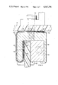
- FIG. 1 is a perspective view of the subject invention
- FIG. 2 is an enlarged detail, partially in section, of one end of the subject invention
- FIG. 3 is a transverse section through the subject invention in an open condition
- FIG. 4 is a transverse, similar of FIG. 3, showing the subject invention in a closed condition
- FIG. 5 is an enlarged detailed perspective view of and end portion of the multi-layer flexible circuit according to the present invention.
- FIG. 6 is a side elevation detail, on an enlarged scale, of the end portions of the multi-layer flexible circuitry according to the present invention.
- FIG. 7 is a schematic representation of the manner in which contact is made between a pad of one of the circuit boards and a contact point on the multi-layer flexible circuit.
- the present invention is a high density mother/daughter circuit board connector.
- the connector 10 is used to interconnect a mother circuit board 12 to a daughter circuit board 14 with each board being provided with circuitry 16, 18 respectively.
- the circuits of the respective boards are preferably terminated by a plurality of contact pads 20, 22 which protrude from the respective surfaces thereof in a patterned array. These could contact pads 20, 22 be in the form of a button or rivet which extends through the respective circuit boards 12, 14.
- the connector 10 includes a housing 24 which is a generally elongated rectangular member having a mother circuit board face 26 and an elongated daughter board receiving recess 28, one side of which is formed as a cam reaction surface 30.
- a multi-layer flexible circuit 32 is wrapped around the face 26 of the housing 24 to lie the daughter board receiving recess 28 on the side 34 opposite the cam reaction surface 30.
- An elongated camming means 26 is also located in the recess 28 to engage against the reaction surface 30.
- the camming means 36 also includes any known cam actuation means 28, here shown as a screw.
- the housing 24 is provided with mounting means 40 for securing it against the mother circuit board 12.
- the housing 24 further has daughter circuit board locating means 42, such as the integral bridge shown in FIG. 1 to assure that the daughter circuit board is properly oriented with respect to the laminate 32.
- the housing 24 is preferably formed of insulative material.
- the multi-layer flexible circuit 32 is best understood from FIGS. 5 through 7. It will be appreciated that the circuit 32 is formed by a plurality of layers of insulating material 44 with at least some of the layers provided with a pattern array of conductors 46 which extend between contact points 48 which are spaced apart on the respective layers but which are aligned with respective contact pads 20, 24 of the mother and daughter circuit boards 12, 14, respectively. One or more of the layers of insulative material are apertured to provide direct access to a contact point of an underlying circuit. It will be appreciated from FIG. 7 that the protruding pads 20, 22 of the circuit boards 12, 14 will extend through the apertures and contact only the exposed contact point 48 layer of the multi-layered flexible circuit 32.
- the assembly of the present invention can best be understood from FIGS. 1 through 4.
- the flexible circuit 32 is wrapped around the housing 24 to overlie the mother circuit board face 26 and to extend into the daughter board receiving recess 28 against side 34.
- the camming means 26 is inserted into the recess 28 against the reaction surface 30 and the thus formed assembly is then secured to the mother circuit board 12 by mounting means 40.
- the daughter board 14 is then inserted into the recess 28, with low or no insertion force.
- the cam actuation means 28 is activated to drive the cam 36 against the rear surface of the daughter circuit board 14 driving its mating face into engagement with the multi-layer flat flexible circuitry 32.
- the pads 22 are of sufficient dimension to make contact with the respective contact points 48. Either or both ends of flexible circuit 32 can be supported on resilient pads 50, 52.
- the present invention is susceptible to a number of variations including different types of camming actions, alignment and centering means, and even two-sided daughter board connection by relocation and doubling of the camming means.
Abstract
Description
Claims (9)
Priority Applications (1)
| Application Number | Priority Date | Filing Date | Title |
|---|---|---|---|
| US06/597,982 US4587596A (en) | 1984-04-09 | 1984-04-09 | High density mother/daughter circuit board connector |
Applications Claiming Priority (1)
| Application Number | Priority Date | Filing Date | Title |
|---|---|---|---|
| US06/597,982 US4587596A (en) | 1984-04-09 | 1984-04-09 | High density mother/daughter circuit board connector |
Publications (1)
| Publication Number | Publication Date |
|---|---|
| US4587596A true US4587596A (en) | 1986-05-06 |
Family
ID=24393765
Family Applications (1)
| Application Number | Title | Priority Date | Filing Date |
|---|---|---|---|
| US06/597,982 Expired - Fee Related US4587596A (en) | 1984-04-09 | 1984-04-09 | High density mother/daughter circuit board connector |
Country Status (1)
| Country | Link |
|---|---|
| US (1) | US4587596A (en) |
Cited By (89)
| Publication number | Priority date | Publication date | Assignee | Title |
|---|---|---|---|---|
| US4635192A (en) * | 1983-12-06 | 1987-01-06 | Tri Sigma Corporation | Self configuring bus structure for computer network |
| US4740867A (en) * | 1987-03-26 | 1988-04-26 | Advanced Circuit Technology, Inc. | Printed circuit connection system |
| US4744764A (en) * | 1986-05-27 | 1988-05-17 | Rogers Corporation | Connector arrangement |
| US4755147A (en) * | 1986-05-20 | 1988-07-05 | Control Data Corporation | Flex head connector with ground plane |
| US4834660A (en) * | 1987-06-03 | 1989-05-30 | Harris Corporation | Flexible zero insertion force interconnector between circuit boards |
| US4861272A (en) * | 1988-03-31 | 1989-08-29 | E. I. Du Pont De Nemours And Company | Impedance controlled connector interface |
| US4878070A (en) * | 1988-10-17 | 1989-10-31 | Xerox Corporation | Thermal ink jet print cartridge assembly |
| US4881908A (en) * | 1988-10-11 | 1989-11-21 | Beta Phase, Inc. | High density and high signal integrity connector |
| US4902234A (en) * | 1988-11-03 | 1990-02-20 | International Business Machines Corporation | Electrical connector assembly including pressure exertion member |
| US4907975A (en) * | 1988-12-19 | 1990-03-13 | International Business Machine Corporation | Electrical connector utilizing flexible electrical circuitry |
| US4911643A (en) * | 1988-10-11 | 1990-03-27 | Beta Phase, Inc. | High density and high signal integrity connector |
| US4933810A (en) * | 1987-04-30 | 1990-06-12 | Honeywell Inc. | Integrated circuit interconnector |
| US4966556A (en) * | 1989-06-13 | 1990-10-30 | General Datacomm, Inc. | Electrical connector for direct connection to plated through holes in circuit board |
| US4976626A (en) * | 1988-12-21 | 1990-12-11 | International Business Machines Corporation | Connector for connecting flexible film circuit carrier to board or card |
| US5002494A (en) * | 1989-05-09 | 1991-03-26 | Amp Incorporated | Printed circuit board edge connector |
| US5057969A (en) * | 1990-09-07 | 1991-10-15 | International Business Machines Corporation | Thin film electronic device |
| US5059129A (en) * | 1991-03-25 | 1991-10-22 | International Business Machines Corporation | Connector assembly including bilayered elastomeric member |
| US5099393A (en) * | 1991-03-25 | 1992-03-24 | International Business Machines Corporation | Electronic package for high density applications |
| US5098309A (en) * | 1991-04-15 | 1992-03-24 | Amp Incorporated | High density connector with contact wipe |
| US5122064A (en) * | 1991-05-23 | 1992-06-16 | Amp Incorporated | Solderless surface-mount electrical connector |
| US5123852A (en) * | 1991-05-17 | 1992-06-23 | International Business Machines Corporation | Modular electrical connector |
| US5126920A (en) * | 1986-05-01 | 1992-06-30 | Honeywell Inc. | Multiple integrated circuit interconnection arrangement |
| USRE34190E (en) * | 1986-05-27 | 1993-03-09 | Rogers Corporation | Connector arrangement |
| US5198965A (en) * | 1991-12-18 | 1993-03-30 | International Business Machines Corporation | Free form packaging of specific functions within a computer system |
| US5215471A (en) * | 1989-06-13 | 1993-06-01 | General Datacomm, Inc. | Electrical connectors having tapered spring contact elements for direct mating to holes |
| US5240420A (en) * | 1992-03-31 | 1993-08-31 | Research Organization For Circuit Knowledge | Self-aligning high-density printed circuit connector |
| US5256073A (en) * | 1989-06-13 | 1993-10-26 | General Datacomm, Inc. | Electrical connectors for direct connection to plated through holes in circuit board |
| US5350319A (en) * | 1993-04-02 | 1994-09-27 | Miraco, Inc. | High-density printed circuit connector |
| US5363275A (en) * | 1993-02-10 | 1994-11-08 | International Business Machines Corporation | Modular component computer system |
| US5366380A (en) * | 1989-06-13 | 1994-11-22 | General Datacomm, Inc. | Spring biased tapered contact elements for electrical connectors and integrated circuit packages |
| US5425649A (en) * | 1989-06-13 | 1995-06-20 | General Datacomm, Inc. | Connector system having switching and testing functions using tapered spring contact elements and actuators therefor |
| EP0720254A3 (en) * | 1994-12-27 | 1996-08-07 | Ibm | |
| US5917709A (en) * | 1997-06-16 | 1999-06-29 | Eastman Kodak Company | Multiple circuit board assembly having an interconnect mechanism that includes a flex connector |
| US20010005042A1 (en) * | 1992-12-11 | 2001-06-28 | Burns Carmen D. | Method of manufacturing a surface mount package |
| US6576992B1 (en) * | 2001-10-26 | 2003-06-10 | Staktek Group L.P. | Chip scale stacking system and method |
| US20030111736A1 (en) * | 2001-12-14 | 2003-06-19 | Roeters Glen E. | Csp chip stack with flex circuit |
| US20040000707A1 (en) * | 2001-10-26 | 2004-01-01 | Staktek Group, L.P. | Modularized die stacking system and method |
| US6727435B1 (en) * | 1996-03-12 | 2004-04-27 | International Business Machines Corporation | Backplane power distribution system |
| US20040191442A1 (en) * | 2003-03-27 | 2004-09-30 | Florencia Lim | Surface modification of expanded ultra high molecular weight polyethylene (eUHMWPE) for improved bondability |
| US20040192077A1 (en) * | 2003-03-24 | 2004-09-30 | Nec Corporation | Apparatus for connecting electronic units together |
| US20040229402A1 (en) * | 2001-10-26 | 2004-11-18 | Staktek Group, L.P. | Low profile chip scale stacking system and method |
| US20040245615A1 (en) * | 2003-06-03 | 2004-12-09 | Staktek Group, L.P. | Point to point memory expansion system and method |
| US20050009234A1 (en) * | 2001-10-26 | 2005-01-13 | Staktek Group, L.P. | Stacked module systems and methods for CSP packages |
| US20050018412A1 (en) * | 2001-10-26 | 2005-01-27 | Staktek Group, L.P. | Pitch change and chip scale stacking system |
| US20050041402A1 (en) * | 2001-10-26 | 2005-02-24 | Staktek Group, L.P. | Integrated circuit stacking system and method |
| US20050056921A1 (en) * | 2003-09-15 | 2005-03-17 | Staktek Group L.P. | Stacked module systems and methods |
| US20050057911A1 (en) * | 2003-09-15 | 2005-03-17 | Staktek Group, L.P. | Memory expansion and integrated circuit stacking system and method |
| US20050062144A1 (en) * | 2001-10-26 | 2005-03-24 | Staktek Group, L.P. | Memory expansion and chip scale stacking system and method |
| US20050146031A1 (en) * | 2001-10-26 | 2005-07-07 | Staktek Group, L.P. | Low profile stacking system and method |
| US20060033187A1 (en) * | 2004-08-12 | 2006-02-16 | Staktek Group, L.P. | Rugged CSP module system and method |
| US7033861B1 (en) | 2005-05-18 | 2006-04-25 | Staktek Group L.P. | Stacked module systems and method |
| US7066741B2 (en) | 1999-09-24 | 2006-06-27 | Staktek Group L.P. | Flexible circuit connector for stacked chip module |
| US20060157842A1 (en) * | 2005-01-20 | 2006-07-20 | Staktek Group L.P. | Inverted CSP stacking system and method |
| US20060250780A1 (en) * | 2005-05-06 | 2006-11-09 | Staktek Group L.P. | System component interposer |
| US20060286858A1 (en) * | 2003-04-30 | 2006-12-21 | Shinji Uchida | Printed wiring board connection structure |
| US7202555B2 (en) | 2001-10-26 | 2007-04-10 | Staktek Group L.P. | Pitch change and chip scale stacking system and method |
| USRE39628E1 (en) | 1999-05-05 | 2007-05-15 | Stakick Group, L.P. | Stackable flex circuit IC package and method of making same |
| US7289327B2 (en) | 2006-02-27 | 2007-10-30 | Stakick Group L.P. | Active cooling methods and apparatus for modules |
| US20070258217A1 (en) * | 2004-09-03 | 2007-11-08 | Roper David L | Split Core Circuit Module |
| US7304382B2 (en) | 2006-01-11 | 2007-12-04 | Staktek Group L.P. | Managed memory component |
| US7310458B2 (en) | 2001-10-26 | 2007-12-18 | Staktek Group L.P. | Stacked module systems and methods |
| US7324352B2 (en) | 2004-09-03 | 2008-01-29 | Staktek Group L.P. | High capacity thin module system and method |
| US20080036068A1 (en) * | 2001-10-26 | 2008-02-14 | Staktek Group L.P. | Stacked Module Systems and Methods |
| US7417310B2 (en) | 2006-11-02 | 2008-08-26 | Entorian Technologies, Lp | Circuit module having force resistant construction |
| US7423885B2 (en) | 2004-09-03 | 2008-09-09 | Entorian Technologies, Lp | Die module system |
| US7443023B2 (en) | 2004-09-03 | 2008-10-28 | Entorian Technologies, Lp | High capacity thin module system |
| US7446410B2 (en) | 2004-09-03 | 2008-11-04 | Entorian Technologies, Lp | Circuit module with thermal casing systems |
| US7468893B2 (en) | 2004-09-03 | 2008-12-23 | Entorian Technologies, Lp | Thin module system and method |
| US7468553B2 (en) | 2006-10-20 | 2008-12-23 | Entorian Technologies, Lp | Stackable micropackages and stacked modules |
| US7480152B2 (en) | 2004-09-03 | 2009-01-20 | Entorian Technologies, Lp | Thin module system and method |
| US7508058B2 (en) | 2006-01-11 | 2009-03-24 | Entorian Technologies, Lp | Stacked integrated circuit module |
| US7508069B2 (en) | 2006-01-11 | 2009-03-24 | Entorian Technologies, Lp | Managed memory component |
| US7511969B2 (en) | 2006-02-02 | 2009-03-31 | Entorian Technologies, Lp | Composite core circuit module system and method |
| US7511968B2 (en) | 2004-09-03 | 2009-03-31 | Entorian Technologies, Lp | Buffered thin module system and method |
| US7524703B2 (en) | 2001-10-26 | 2009-04-28 | Entorian Technologies, Lp | Integrated circuit stacking system and method |
| US7542297B2 (en) | 2004-09-03 | 2009-06-02 | Entorian Technologies, Lp | Optimized mounting area circuit module system and method |
| US7576995B2 (en) | 2005-11-04 | 2009-08-18 | Entorian Technologies, Lp | Flex circuit apparatus and method for adding capacitance while conserving circuit board surface area |
| US7579687B2 (en) | 2004-09-03 | 2009-08-25 | Entorian Technologies, Lp | Circuit module turbulence enhancement systems and methods |
| US7606049B2 (en) | 2004-09-03 | 2009-10-20 | Entorian Technologies, Lp | Module thermal management system and method |
| US7605454B2 (en) | 2006-01-11 | 2009-10-20 | Entorian Technologies, Lp | Memory card and method for devising |
| US7606050B2 (en) | 2004-09-03 | 2009-10-20 | Entorian Technologies, Lp | Compact module system and method |
| US7606040B2 (en) | 2004-09-03 | 2009-10-20 | Entorian Technologies, Lp | Memory module system and method |
| US7608920B2 (en) | 2006-01-11 | 2009-10-27 | Entorian Technologies, Lp | Memory card and method for devising |
| US7616452B2 (en) | 2004-09-03 | 2009-11-10 | Entorian Technologies, Lp | Flex circuit constructions for high capacity circuit module systems and methods |
| USRE41039E1 (en) | 2000-01-13 | 2009-12-15 | Entorian Technologies, Lp | Stackable chip package with flex carrier |
| US7656678B2 (en) | 2001-10-26 | 2010-02-02 | Entorian Technologies, Lp | Stacked module systems |
| US7719098B2 (en) | 2001-10-26 | 2010-05-18 | Entorian Technologies Lp | Stacked modules and method |
| US7760513B2 (en) | 2004-09-03 | 2010-07-20 | Entorian Technologies Lp | Modified core for circuit module system and method |
| US20110070748A1 (en) * | 2009-09-21 | 2011-03-24 | Teradyne, Inc. | Methods and apparatus for connecting printed circuit boards using zero-insertion wiping force connectors |
Citations (8)
| Publication number | Priority date | Publication date | Assignee | Title |
|---|---|---|---|---|
| US3401369A (en) * | 1966-06-07 | 1968-09-10 | Ibm | Connector |
| US3489990A (en) * | 1966-07-14 | 1970-01-13 | Litton Business Systems Inc | Multipurpose coupling device |
| US3609463A (en) * | 1968-10-01 | 1971-09-28 | Bull General Electric | Connectors for printed-circuit cards |
| US3772775A (en) * | 1972-07-17 | 1973-11-20 | Methods Electronics Inc | Method of making flat conductor cable assemblies |
| US3922054A (en) * | 1973-09-14 | 1975-11-25 | Amp Inc | Printed circuit electrical connector |
| US3967162A (en) * | 1974-07-24 | 1976-06-29 | Amp Incorporated | Interconnection of oppositely disposed circuit devices |
| US4116516A (en) * | 1977-06-24 | 1978-09-26 | Gte Sylvania Incorporated | Multiple layered connector |
| US4211459A (en) * | 1979-02-26 | 1980-07-08 | Bell Telephone Laboratories, Incorporated | Circuit board interconnection apparatus |
-
1984
- 1984-04-09 US US06/597,982 patent/US4587596A/en not_active Expired - Fee Related
Patent Citations (8)
| Publication number | Priority date | Publication date | Assignee | Title |
|---|---|---|---|---|
| US3401369A (en) * | 1966-06-07 | 1968-09-10 | Ibm | Connector |
| US3489990A (en) * | 1966-07-14 | 1970-01-13 | Litton Business Systems Inc | Multipurpose coupling device |
| US3609463A (en) * | 1968-10-01 | 1971-09-28 | Bull General Electric | Connectors for printed-circuit cards |
| US3772775A (en) * | 1972-07-17 | 1973-11-20 | Methods Electronics Inc | Method of making flat conductor cable assemblies |
| US3922054A (en) * | 1973-09-14 | 1975-11-25 | Amp Inc | Printed circuit electrical connector |
| US3967162A (en) * | 1974-07-24 | 1976-06-29 | Amp Incorporated | Interconnection of oppositely disposed circuit devices |
| US4116516A (en) * | 1977-06-24 | 1978-09-26 | Gte Sylvania Incorporated | Multiple layered connector |
| US4211459A (en) * | 1979-02-26 | 1980-07-08 | Bell Telephone Laboratories, Incorporated | Circuit board interconnection apparatus |
Non-Patent Citations (2)
| Title |
|---|
| Hinrichsmeyer et al, Combined Action Zero Insertion Force Connector, IBM Tech. Disc. Bull., vol. 26, #12, May 1984, pp. 6476 and 6477. |
| Hinrichsmeyer et al, Combined Action Zero Insertion Force Connector, IBM Tech. Disc. Bull., vol. 26, 12, May 1984, pp. 6476 and 6477. * |
Cited By (133)
| Publication number | Priority date | Publication date | Assignee | Title |
|---|---|---|---|---|
| US4635192A (en) * | 1983-12-06 | 1987-01-06 | Tri Sigma Corporation | Self configuring bus structure for computer network |
| US5126920A (en) * | 1986-05-01 | 1992-06-30 | Honeywell Inc. | Multiple integrated circuit interconnection arrangement |
| US4755147A (en) * | 1986-05-20 | 1988-07-05 | Control Data Corporation | Flex head connector with ground plane |
| US4744764A (en) * | 1986-05-27 | 1988-05-17 | Rogers Corporation | Connector arrangement |
| USRE34190E (en) * | 1986-05-27 | 1993-03-09 | Rogers Corporation | Connector arrangement |
| US4740867A (en) * | 1987-03-26 | 1988-04-26 | Advanced Circuit Technology, Inc. | Printed circuit connection system |
| US4933810A (en) * | 1987-04-30 | 1990-06-12 | Honeywell Inc. | Integrated circuit interconnector |
| US4834660A (en) * | 1987-06-03 | 1989-05-30 | Harris Corporation | Flexible zero insertion force interconnector between circuit boards |
| US4861272A (en) * | 1988-03-31 | 1989-08-29 | E. I. Du Pont De Nemours And Company | Impedance controlled connector interface |
| US5015193A (en) * | 1988-10-11 | 1991-05-14 | Beta Phase, Inc. | High density and high signal integrity connector |
| US4881908A (en) * | 1988-10-11 | 1989-11-21 | Beta Phase, Inc. | High density and high signal integrity connector |
| US4911643A (en) * | 1988-10-11 | 1990-03-27 | Beta Phase, Inc. | High density and high signal integrity connector |
| WO1990004270A1 (en) * | 1988-10-11 | 1990-04-19 | Beta Phase, Inc. | High density and high signal integrity connector |
| US4878070A (en) * | 1988-10-17 | 1989-10-31 | Xerox Corporation | Thermal ink jet print cartridge assembly |
| US4902234A (en) * | 1988-11-03 | 1990-02-20 | International Business Machines Corporation | Electrical connector assembly including pressure exertion member |
| US4907975A (en) * | 1988-12-19 | 1990-03-13 | International Business Machine Corporation | Electrical connector utilizing flexible electrical circuitry |
| EP0374460A2 (en) * | 1988-12-19 | 1990-06-27 | International Business Machines Corporation | Electric connector utilizing flexible electrical circuitry |
| EP0374460A3 (en) * | 1988-12-19 | 1990-12-27 | International Business Machines Corporation | Electric connector utilizing flexible electrical circuitry |
| US4976626A (en) * | 1988-12-21 | 1990-12-11 | International Business Machines Corporation | Connector for connecting flexible film circuit carrier to board or card |
| US5002494A (en) * | 1989-05-09 | 1991-03-26 | Amp Incorporated | Printed circuit board edge connector |
| US5425649A (en) * | 1989-06-13 | 1995-06-20 | General Datacomm, Inc. | Connector system having switching and testing functions using tapered spring contact elements and actuators therefor |
| US5366380A (en) * | 1989-06-13 | 1994-11-22 | General Datacomm, Inc. | Spring biased tapered contact elements for electrical connectors and integrated circuit packages |
| US5256073A (en) * | 1989-06-13 | 1993-10-26 | General Datacomm, Inc. | Electrical connectors for direct connection to plated through holes in circuit board |
| US5215471A (en) * | 1989-06-13 | 1993-06-01 | General Datacomm, Inc. | Electrical connectors having tapered spring contact elements for direct mating to holes |
| US4966556A (en) * | 1989-06-13 | 1990-10-30 | General Datacomm, Inc. | Electrical connector for direct connection to plated through holes in circuit board |
| US5057969A (en) * | 1990-09-07 | 1991-10-15 | International Business Machines Corporation | Thin film electronic device |
| US5099393A (en) * | 1991-03-25 | 1992-03-24 | International Business Machines Corporation | Electronic package for high density applications |
| US5059129A (en) * | 1991-03-25 | 1991-10-22 | International Business Machines Corporation | Connector assembly including bilayered elastomeric member |
| US5098309A (en) * | 1991-04-15 | 1992-03-24 | Amp Incorporated | High density connector with contact wipe |
| US5123852A (en) * | 1991-05-17 | 1992-06-23 | International Business Machines Corporation | Modular electrical connector |
| US5122064A (en) * | 1991-05-23 | 1992-06-16 | Amp Incorporated | Solderless surface-mount electrical connector |
| US5198965A (en) * | 1991-12-18 | 1993-03-30 | International Business Machines Corporation | Free form packaging of specific functions within a computer system |
| US5240420A (en) * | 1992-03-31 | 1993-08-31 | Research Organization For Circuit Knowledge | Self-aligning high-density printed circuit connector |
| US5306160A (en) * | 1992-03-31 | 1994-04-26 | Rock Ltd. Partnership | Self-aligning high-density printed circuit connector |
| US20010005042A1 (en) * | 1992-12-11 | 2001-06-28 | Burns Carmen D. | Method of manufacturing a surface mount package |
| US6919626B2 (en) | 1992-12-11 | 2005-07-19 | Staktek Group L.P. | High density integrated circuit module |
| US5363275A (en) * | 1993-02-10 | 1994-11-08 | International Business Machines Corporation | Modular component computer system |
| US5350319A (en) * | 1993-04-02 | 1994-09-27 | Miraco, Inc. | High-density printed circuit connector |
| US5871362A (en) * | 1994-12-27 | 1999-02-16 | International Business Machines Corporation | Self-aligning flexible circuit connection |
| EP0720254A3 (en) * | 1994-12-27 | 1996-08-07 | Ibm | |
| US6727435B1 (en) * | 1996-03-12 | 2004-04-27 | International Business Machines Corporation | Backplane power distribution system |
| US5917709A (en) * | 1997-06-16 | 1999-06-29 | Eastman Kodak Company | Multiple circuit board assembly having an interconnect mechanism that includes a flex connector |
| USRE39628E1 (en) | 1999-05-05 | 2007-05-15 | Stakick Group, L.P. | Stackable flex circuit IC package and method of making same |
| US7066741B2 (en) | 1999-09-24 | 2006-06-27 | Staktek Group L.P. | Flexible circuit connector for stacked chip module |
| USRE41039E1 (en) | 2000-01-13 | 2009-12-15 | Entorian Technologies, Lp | Stackable chip package with flex carrier |
| US20050280135A1 (en) * | 2001-10-26 | 2005-12-22 | Staktek Group L.P. | Stacking system and method |
| US7572671B2 (en) | 2001-10-26 | 2009-08-11 | Entorian Technologies, Lp | Stacked module systems and methods |
| US20040229402A1 (en) * | 2001-10-26 | 2004-11-18 | Staktek Group, L.P. | Low profile chip scale stacking system and method |
| US7719098B2 (en) | 2001-10-26 | 2010-05-18 | Entorian Technologies Lp | Stacked modules and method |
| US20050009234A1 (en) * | 2001-10-26 | 2005-01-13 | Staktek Group, L.P. | Stacked module systems and methods for CSP packages |
| US20050018412A1 (en) * | 2001-10-26 | 2005-01-27 | Staktek Group, L.P. | Pitch change and chip scale stacking system |
| US20050041402A1 (en) * | 2001-10-26 | 2005-02-24 | Staktek Group, L.P. | Integrated circuit stacking system and method |
| US7626273B2 (en) | 2001-10-26 | 2009-12-01 | Entorian Technologies, L.P. | Low profile stacking system and method |
| US7606048B2 (en) | 2001-10-26 | 2009-10-20 | Enthorian Technologies, LP | Integrated circuit stacking system |
| US20050062144A1 (en) * | 2001-10-26 | 2005-03-24 | Staktek Group, L.P. | Memory expansion and chip scale stacking system and method |
| US20050067683A1 (en) * | 2001-10-26 | 2005-03-31 | Staktek Group L.P. | Memory expansion and chip scale stacking system and method |
| US7595550B2 (en) | 2001-10-26 | 2009-09-29 | Entorian Technologies, Lp | Flex-based circuit module |
| US20050146031A1 (en) * | 2001-10-26 | 2005-07-07 | Staktek Group, L.P. | Low profile stacking system and method |
| US7310458B2 (en) | 2001-10-26 | 2007-12-18 | Staktek Group L.P. | Stacked module systems and methods |
| US20040000707A1 (en) * | 2001-10-26 | 2004-01-01 | Staktek Group, L.P. | Modularized die stacking system and method |
| US7586758B2 (en) | 2001-10-26 | 2009-09-08 | Entorian Technologies, Lp | Integrated circuit stacking system |
| US7026708B2 (en) | 2001-10-26 | 2006-04-11 | Staktek Group L.P. | Low profile chip scale stacking system and method |
| US7656678B2 (en) | 2001-10-26 | 2010-02-02 | Entorian Technologies, Lp | Stacked module systems |
| US7053478B2 (en) | 2001-10-26 | 2006-05-30 | Staktek Group L.P. | Pitch change and chip scale stacking system |
| US20030137048A1 (en) * | 2001-10-26 | 2003-07-24 | Staktek Group, L.P. | Stacking system and method |
| US7524703B2 (en) | 2001-10-26 | 2009-04-28 | Entorian Technologies, Lp | Integrated circuit stacking system and method |
| US20080036068A1 (en) * | 2001-10-26 | 2008-02-14 | Staktek Group L.P. | Stacked Module Systems and Methods |
| US7335975B2 (en) | 2001-10-26 | 2008-02-26 | Staktek Group L.P. | Integrated circuit stacking system and method |
| US7094632B2 (en) | 2001-10-26 | 2006-08-22 | Staktek Group L.P. | Low profile chip scale stacking system and method |
| US7495334B2 (en) | 2001-10-26 | 2009-02-24 | Entorian Technologies, Lp | Stacking system and method |
| US7485951B2 (en) | 2001-10-26 | 2009-02-03 | Entorian Technologies, Lp | Modularized die stacking system and method |
| US7180167B2 (en) | 2001-10-26 | 2007-02-20 | Staktek Group L. P. | Low profile stacking system and method |
| US7256484B2 (en) | 2001-10-26 | 2007-08-14 | Staktek Group L.P. | Memory expansion and chip scale stacking system and method |
| US7202555B2 (en) | 2001-10-26 | 2007-04-10 | Staktek Group L.P. | Pitch change and chip scale stacking system and method |
| US6576992B1 (en) * | 2001-10-26 | 2003-06-10 | Staktek Group L.P. | Chip scale stacking system and method |
| US7371609B2 (en) | 2001-10-26 | 2008-05-13 | Staktek Group L.P. | Stacked module systems and methods |
| US7193310B2 (en) | 2001-12-14 | 2007-03-20 | Stuktek Group L.P. | Stacking system and method |
| US20030111736A1 (en) * | 2001-12-14 | 2003-06-19 | Roeters Glen E. | Csp chip stack with flex circuit |
| US7081373B2 (en) | 2001-12-14 | 2006-07-25 | Staktek Group, L.P. | CSP chip stack with flex circuit |
| US7080987B2 (en) * | 2003-03-24 | 2006-07-25 | Nec Corporation | Apparatus for connecting electronic units together |
| US20040192077A1 (en) * | 2003-03-24 | 2004-09-30 | Nec Corporation | Apparatus for connecting electronic units together |
| US20040191442A1 (en) * | 2003-03-27 | 2004-09-30 | Florencia Lim | Surface modification of expanded ultra high molecular weight polyethylene (eUHMWPE) for improved bondability |
| US20060286858A1 (en) * | 2003-04-30 | 2006-12-21 | Shinji Uchida | Printed wiring board connection structure |
| US7232315B2 (en) * | 2003-04-30 | 2007-06-19 | J.S.T. Mfg. Co., Ltd. | Connection structure for printed wiring board |
| US20040245615A1 (en) * | 2003-06-03 | 2004-12-09 | Staktek Group, L.P. | Point to point memory expansion system and method |
| US20050056921A1 (en) * | 2003-09-15 | 2005-03-17 | Staktek Group L.P. | Stacked module systems and methods |
| US20050057911A1 (en) * | 2003-09-15 | 2005-03-17 | Staktek Group, L.P. | Memory expansion and integrated circuit stacking system and method |
| US20050098873A1 (en) * | 2003-09-15 | 2005-05-12 | Staktek Group L.P. | Stacked module systems and methods |
| US7542304B2 (en) | 2003-09-15 | 2009-06-02 | Entorian Technologies, Lp | Memory expansion and integrated circuit stacking system and method |
| US20060033187A1 (en) * | 2004-08-12 | 2006-02-16 | Staktek Group, L.P. | Rugged CSP module system and method |
| US7626259B2 (en) | 2004-09-03 | 2009-12-01 | Entorian Technologies, Lp | Heat sink for a high capacity thin module system |
| US7602613B2 (en) | 2004-09-03 | 2009-10-13 | Entorian Technologies, Lp | Thin module system and method |
| US7468893B2 (en) | 2004-09-03 | 2008-12-23 | Entorian Technologies, Lp | Thin module system and method |
| US7768796B2 (en) | 2004-09-03 | 2010-08-03 | Entorian Technologies L.P. | Die module system |
| US7480152B2 (en) | 2004-09-03 | 2009-01-20 | Entorian Technologies, Lp | Thin module system and method |
| US7446410B2 (en) | 2004-09-03 | 2008-11-04 | Entorian Technologies, Lp | Circuit module with thermal casing systems |
| US7760513B2 (en) | 2004-09-03 | 2010-07-20 | Entorian Technologies Lp | Modified core for circuit module system and method |
| US7737549B2 (en) | 2004-09-03 | 2010-06-15 | Entorian Technologies Lp | Circuit module with thermal casing systems |
| US7324352B2 (en) | 2004-09-03 | 2008-01-29 | Staktek Group L.P. | High capacity thin module system and method |
| US20070258217A1 (en) * | 2004-09-03 | 2007-11-08 | Roper David L | Split Core Circuit Module |
| US7511968B2 (en) | 2004-09-03 | 2009-03-31 | Entorian Technologies, Lp | Buffered thin module system and method |
| US7522421B2 (en) | 2004-09-03 | 2009-04-21 | Entorian Technologies, Lp | Split core circuit module |
| US7522425B2 (en) | 2004-09-03 | 2009-04-21 | Entorian Technologies, Lp | High capacity thin module system and method |
| US7616452B2 (en) | 2004-09-03 | 2009-11-10 | Entorian Technologies, Lp | Flex circuit constructions for high capacity circuit module systems and methods |
| US7443023B2 (en) | 2004-09-03 | 2008-10-28 | Entorian Technologies, Lp | High capacity thin module system |
| US7542297B2 (en) | 2004-09-03 | 2009-06-02 | Entorian Technologies, Lp | Optimized mounting area circuit module system and method |
| US7606040B2 (en) | 2004-09-03 | 2009-10-20 | Entorian Technologies, Lp | Memory module system and method |
| US7606050B2 (en) | 2004-09-03 | 2009-10-20 | Entorian Technologies, Lp | Compact module system and method |
| US7579687B2 (en) | 2004-09-03 | 2009-08-25 | Entorian Technologies, Lp | Circuit module turbulence enhancement systems and methods |
| US7423885B2 (en) | 2004-09-03 | 2008-09-09 | Entorian Technologies, Lp | Die module system |
| US7606042B2 (en) | 2004-09-03 | 2009-10-20 | Entorian Technologies, Lp | High capacity thin module system and method |
| US7459784B2 (en) | 2004-09-03 | 2008-12-02 | Entorian Technologies, Lp | High capacity thin module system |
| US7606049B2 (en) | 2004-09-03 | 2009-10-20 | Entorian Technologies, Lp | Module thermal management system and method |
| US20060157842A1 (en) * | 2005-01-20 | 2006-07-20 | Staktek Group L.P. | Inverted CSP stacking system and method |
| US7309914B2 (en) | 2005-01-20 | 2007-12-18 | Staktek Group L.P. | Inverted CSP stacking system and method |
| US20060250780A1 (en) * | 2005-05-06 | 2006-11-09 | Staktek Group L.P. | System component interposer |
| US7323364B2 (en) | 2005-05-18 | 2008-01-29 | Staktek Group L.P. | Stacked module systems and method |
| US7033861B1 (en) | 2005-05-18 | 2006-04-25 | Staktek Group L.P. | Stacked module systems and method |
| US7576995B2 (en) | 2005-11-04 | 2009-08-18 | Entorian Technologies, Lp | Flex circuit apparatus and method for adding capacitance while conserving circuit board surface area |
| US7608920B2 (en) | 2006-01-11 | 2009-10-27 | Entorian Technologies, Lp | Memory card and method for devising |
| US7508069B2 (en) | 2006-01-11 | 2009-03-24 | Entorian Technologies, Lp | Managed memory component |
| US7605454B2 (en) | 2006-01-11 | 2009-10-20 | Entorian Technologies, Lp | Memory card and method for devising |
| US7304382B2 (en) | 2006-01-11 | 2007-12-04 | Staktek Group L.P. | Managed memory component |
| US7508058B2 (en) | 2006-01-11 | 2009-03-24 | Entorian Technologies, Lp | Stacked integrated circuit module |
| US7511969B2 (en) | 2006-02-02 | 2009-03-31 | Entorian Technologies, Lp | Composite core circuit module system and method |
| US7289327B2 (en) | 2006-02-27 | 2007-10-30 | Stakick Group L.P. | Active cooling methods and apparatus for modules |
| US7468553B2 (en) | 2006-10-20 | 2008-12-23 | Entorian Technologies, Lp | Stackable micropackages and stacked modules |
| US7417310B2 (en) | 2006-11-02 | 2008-08-26 | Entorian Technologies, Lp | Circuit module having force resistant construction |
| US7804985B2 (en) | 2006-11-02 | 2010-09-28 | Entorian Technologies Lp | Circuit module having force resistant construction |
| US20110070748A1 (en) * | 2009-09-21 | 2011-03-24 | Teradyne, Inc. | Methods and apparatus for connecting printed circuit boards using zero-insertion wiping force connectors |
| US8128417B2 (en) * | 2009-09-21 | 2012-03-06 | Teradyne, Inc. | Methods and apparatus for connecting printed circuit boards using zero-insertion wiping force connectors |
| CN102498623A (en) * | 2009-09-21 | 2012-06-13 | 泰拉丁公司 | Methods and apparatus for connecting printed circuit boards using zero-insertion wiping force connectors |
| CN102498623B (en) * | 2009-09-21 | 2014-10-15 | 泰拉丁公司 | Methods and apparatus for connecting printed circuit boards using zero-insertion wiping force connectors |
Similar Documents
| Publication | Publication Date | Title |
|---|---|---|
| US4587596A (en) | High density mother/daughter circuit board connector | |
| US4560221A (en) | High density zero insertion force connector | |
| US5766023A (en) | Electrical connector with high speed and high density contact strip | |
| US4487464A (en) | Electrical socket connector construction | |
| US6183301B1 (en) | Surface mount connector with integrated PCB assembly | |
| US4087146A (en) | Flat flexible cable surface mount connector assembly | |
| US4116516A (en) | Multiple layered connector | |
| EP0107288B1 (en) | Electrical connector assembly for terminating flat shielded electrical cable | |
| US4517625A (en) | Circuit board housing with zero insertion force connector | |
| US4784615A (en) | Direct contact flexible circuit interconnect system and method | |
| US5727956A (en) | Connector assembly including metal strips as contact members | |
| US6162083A (en) | Electrical connector system for flat circuitry | |
| US5161981A (en) | Foldable stacking connector | |
| US5947764A (en) | Connector assembly with a connecting means to board and arranging method for the same | |
| US4798541A (en) | Right angle electrical connector | |
| US4815979A (en) | Right angle electrical connector with or without wiping action | |
| JPH06208874A (en) | Electrical connector for card reader | |
| US3868162A (en) | Electrical connector | |
| KR0122783Y1 (en) | Electrical connector for printed circuit board or the like | |
| US4538878A (en) | Solderless circuit board connector | |
| US5702269A (en) | Electrical connector | |
| EP0409463B1 (en) | Electrical connector for connecting heat seal film to a printed wiring board | |
| US5588849A (en) | Connector with pin terminals adapted for surface mounting | |
| US6739878B1 (en) | Pressure point contact for flexible cable | |
| US5964594A (en) | Electrical connector |
Legal Events
| Date | Code | Title | Description |
|---|---|---|---|
| AS | Assignment |
Owner name: AMP INCORPORATED, P.O. BOX 3608, HARRISBURG, PA 1 Free format text: ASSIGNMENT OF ASSIGNORS INTEREST.;ASSIGNOR:BUNNELL, EDWARD D.;REEL/FRAME:004248/0290 Effective date: 19840402 |
|
| FEPP | Fee payment procedure |
Free format text: PAYOR NUMBER ASSIGNED (ORIGINAL EVENT CODE: ASPN); ENTITY STATUS OF PATENT OWNER: LARGE ENTITY |
|
| FPAY | Fee payment |
Year of fee payment: 4 |
|
| FEPP | Fee payment procedure |
Free format text: PAYOR NUMBER ASSIGNED (ORIGINAL EVENT CODE: ASPN); ENTITY STATUS OF PATENT OWNER: LARGE ENTITY Free format text: PAYER NUMBER DE-ASSIGNED (ORIGINAL EVENT CODE: RMPN); ENTITY STATUS OF PATENT OWNER: LARGE ENTITY |
|
| FPAY | Fee payment |
Year of fee payment: 8 |
|
| REMI | Maintenance fee reminder mailed | ||
| LAPS | Lapse for failure to pay maintenance fees | ||
| FP | Lapsed due to failure to pay maintenance fee |
Effective date: 19980506 |
|
| STCH | Information on status: patent discontinuation |
Free format text: PATENT EXPIRED DUE TO NONPAYMENT OF MAINTENANCE FEES UNDER 37 CFR 1.362 |