US4589010A - Method for manufacturing a plastic encapsulated semiconductor device and a lead frame therefor - Google Patents
Method for manufacturing a plastic encapsulated semiconductor device and a lead frame therefor Download PDFInfo
- Publication number
- US4589010A US4589010A US06/581,251 US58125184A US4589010A US 4589010 A US4589010 A US 4589010A US 58125184 A US58125184 A US 58125184A US 4589010 A US4589010 A US 4589010A
- Authority
- US
- United States
- Prior art keywords
- strips
- substrate support
- lead frame
- plastic
- portions
- Prior art date
- Legal status (The legal status is an assumption and is not a legal conclusion. Google has not performed a legal analysis and makes no representation as to the accuracy of the status listed.)
- Expired - Lifetime
Links
Images


Classifications
-
- H—ELECTRICITY
- H01—ELECTRIC ELEMENTS
- H01L—SEMICONDUCTOR DEVICES NOT COVERED BY CLASS H10
- H01L23/00—Details of semiconductor or other solid state devices
- H01L23/28—Encapsulations, e.g. encapsulating layers, coatings, e.g. for protection
- H01L23/31—Encapsulations, e.g. encapsulating layers, coatings, e.g. for protection characterised by the arrangement or shape
- H01L23/3107—Encapsulations, e.g. encapsulating layers, coatings, e.g. for protection characterised by the arrangement or shape the device being completely enclosed
-
- H—ELECTRICITY
- H01—ELECTRIC ELEMENTS
- H01L—SEMICONDUCTOR DEVICES NOT COVERED BY CLASS H10
- H01L21/00—Processes or apparatus adapted for the manufacture or treatment of semiconductor or solid state devices or of parts thereof
- H01L21/02—Manufacture or treatment of semiconductor devices or of parts thereof
- H01L21/04—Manufacture or treatment of semiconductor devices or of parts thereof the devices having at least one potential-jump barrier or surface barrier, e.g. PN junction, depletion layer or carrier concentration layer
- H01L21/50—Assembly of semiconductor devices using processes or apparatus not provided for in a single one of the subgroups H01L21/06 - H01L21/326, e.g. sealing of a cap to a base of a container
- H01L21/56—Encapsulations, e.g. encapsulation layers, coatings
- H01L21/565—Moulds
-
- H—ELECTRICITY
- H01—ELECTRIC ELEMENTS
- H01L—SEMICONDUCTOR DEVICES NOT COVERED BY CLASS H10
- H01L23/00—Details of semiconductor or other solid state devices
- H01L23/28—Encapsulations, e.g. encapsulating layers, coatings, e.g. for protection
- H01L23/31—Encapsulations, e.g. encapsulating layers, coatings, e.g. for protection characterised by the arrangement or shape
- H01L23/3107—Encapsulations, e.g. encapsulating layers, coatings, e.g. for protection characterised by the arrangement or shape the device being completely enclosed
- H01L23/3135—Double encapsulation or coating and encapsulation
-
- H—ELECTRICITY
- H01—ELECTRIC ELEMENTS
- H01L—SEMICONDUCTOR DEVICES NOT COVERED BY CLASS H10
- H01L23/00—Details of semiconductor or other solid state devices
- H01L23/48—Arrangements for conducting electric current to or from the solid state body in operation, e.g. leads, terminal arrangements ; Selection of materials therefor
- H01L23/488—Arrangements for conducting electric current to or from the solid state body in operation, e.g. leads, terminal arrangements ; Selection of materials therefor consisting of soldered or bonded constructions
- H01L23/495—Lead-frames or other flat leads
- H01L23/49541—Geometry of the lead-frame
- H01L23/49562—Geometry of the lead-frame for devices being provided for in H01L29/00
-
- H—ELECTRICITY
- H01—ELECTRIC ELEMENTS
- H01L—SEMICONDUCTOR DEVICES NOT COVERED BY CLASS H10
- H01L24/00—Arrangements for connecting or disconnecting semiconductor or solid-state bodies; Methods or apparatus related thereto
- H01L24/93—Batch processes
- H01L24/95—Batch processes at chip-level, i.e. with connecting carried out on a plurality of singulated devices, i.e. on diced chips
- H01L24/97—Batch processes at chip-level, i.e. with connecting carried out on a plurality of singulated devices, i.e. on diced chips the devices being connected to a common substrate, e.g. interposer, said common substrate being separable into individual assemblies after connecting
-
- H—ELECTRICITY
- H01—ELECTRIC ELEMENTS
- H01L—SEMICONDUCTOR DEVICES NOT COVERED BY CLASS H10
- H01L2224/00—Indexing scheme for arrangements for connecting or disconnecting semiconductor or solid-state bodies and methods related thereto as covered by H01L24/00
- H01L2224/01—Means for bonding being attached to, or being formed on, the surface to be connected, e.g. chip-to-package, die-attach, "first-level" interconnects; Manufacturing methods related thereto
- H01L2224/02—Bonding areas; Manufacturing methods related thereto
- H01L2224/04—Structure, shape, material or disposition of the bonding areas prior to the connecting process
- H01L2224/05—Structure, shape, material or disposition of the bonding areas prior to the connecting process of an individual bonding area
- H01L2224/0554—External layer
- H01L2224/0555—Shape
- H01L2224/05552—Shape in top view
- H01L2224/05554—Shape in top view being square
-
- H—ELECTRICITY
- H01—ELECTRIC ELEMENTS
- H01L—SEMICONDUCTOR DEVICES NOT COVERED BY CLASS H10
- H01L2224/00—Indexing scheme for arrangements for connecting or disconnecting semiconductor or solid-state bodies and methods related thereto as covered by H01L24/00
- H01L2224/01—Means for bonding being attached to, or being formed on, the surface to be connected, e.g. chip-to-package, die-attach, "first-level" interconnects; Manufacturing methods related thereto
- H01L2224/42—Wire connectors; Manufacturing methods related thereto
- H01L2224/44—Structure, shape, material or disposition of the wire connectors prior to the connecting process
- H01L2224/45—Structure, shape, material or disposition of the wire connectors prior to the connecting process of an individual wire connector
- H01L2224/45001—Core members of the connector
- H01L2224/45099—Material
- H01L2224/451—Material with a principal constituent of the material being a metal or a metalloid, e.g. boron (B), silicon (Si), germanium (Ge), arsenic (As), antimony (Sb), tellurium (Te) and polonium (Po), and alloys thereof
-
- H—ELECTRICITY
- H01—ELECTRIC ELEMENTS
- H01L—SEMICONDUCTOR DEVICES NOT COVERED BY CLASS H10
- H01L2224/00—Indexing scheme for arrangements for connecting or disconnecting semiconductor or solid-state bodies and methods related thereto as covered by H01L24/00
- H01L2224/01—Means for bonding being attached to, or being formed on, the surface to be connected, e.g. chip-to-package, die-attach, "first-level" interconnects; Manufacturing methods related thereto
- H01L2224/42—Wire connectors; Manufacturing methods related thereto
- H01L2224/47—Structure, shape, material or disposition of the wire connectors after the connecting process
- H01L2224/48—Structure, shape, material or disposition of the wire connectors after the connecting process of an individual wire connector
- H01L2224/4805—Shape
- H01L2224/4809—Loop shape
- H01L2224/48091—Arched
-
- H—ELECTRICITY
- H01—ELECTRIC ELEMENTS
- H01L—SEMICONDUCTOR DEVICES NOT COVERED BY CLASS H10
- H01L2224/00—Indexing scheme for arrangements for connecting or disconnecting semiconductor or solid-state bodies and methods related thereto as covered by H01L24/00
- H01L2224/01—Means for bonding being attached to, or being formed on, the surface to be connected, e.g. chip-to-package, die-attach, "first-level" interconnects; Manufacturing methods related thereto
- H01L2224/42—Wire connectors; Manufacturing methods related thereto
- H01L2224/47—Structure, shape, material or disposition of the wire connectors after the connecting process
- H01L2224/48—Structure, shape, material or disposition of the wire connectors after the connecting process of an individual wire connector
- H01L2224/481—Disposition
- H01L2224/48151—Connecting between a semiconductor or solid-state body and an item not being a semiconductor or solid-state body, e.g. chip-to-substrate, chip-to-passive
- H01L2224/48221—Connecting between a semiconductor or solid-state body and an item not being a semiconductor or solid-state body, e.g. chip-to-substrate, chip-to-passive the body and the item being stacked
- H01L2224/48245—Connecting between a semiconductor or solid-state body and an item not being a semiconductor or solid-state body, e.g. chip-to-substrate, chip-to-passive the body and the item being stacked the item being metallic
- H01L2224/48247—Connecting between a semiconductor or solid-state body and an item not being a semiconductor or solid-state body, e.g. chip-to-substrate, chip-to-passive the body and the item being stacked the item being metallic connecting the wire to a bond pad of the item
-
- H—ELECTRICITY
- H01—ELECTRIC ELEMENTS
- H01L—SEMICONDUCTOR DEVICES NOT COVERED BY CLASS H10
- H01L2224/00—Indexing scheme for arrangements for connecting or disconnecting semiconductor or solid-state bodies and methods related thereto as covered by H01L24/00
- H01L2224/80—Methods for connecting semiconductor or other solid state bodies using means for bonding being attached to, or being formed on, the surface to be connected
- H01L2224/85—Methods for connecting semiconductor or other solid state bodies using means for bonding being attached to, or being formed on, the surface to be connected using a wire connector
- H01L2224/85909—Post-treatment of the connector or wire bonding area
- H01L2224/8592—Applying permanent coating, e.g. protective coating
-
- H—ELECTRICITY
- H01—ELECTRIC ELEMENTS
- H01L—SEMICONDUCTOR DEVICES NOT COVERED BY CLASS H10
- H01L2224/00—Indexing scheme for arrangements for connecting or disconnecting semiconductor or solid-state bodies and methods related thereto as covered by H01L24/00
- H01L2224/93—Batch processes
- H01L2224/95—Batch processes at chip-level, i.e. with connecting carried out on a plurality of singulated devices, i.e. on diced chips
- H01L2224/97—Batch processes at chip-level, i.e. with connecting carried out on a plurality of singulated devices, i.e. on diced chips the devices being connected to a common substrate, e.g. interposer, said common substrate being separable into individual assemblies after connecting
-
- H—ELECTRICITY
- H01—ELECTRIC ELEMENTS
- H01L—SEMICONDUCTOR DEVICES NOT COVERED BY CLASS H10
- H01L24/00—Arrangements for connecting or disconnecting semiconductor or solid-state bodies; Methods or apparatus related thereto
- H01L24/01—Means for bonding being attached to, or being formed on, the surface to be connected, e.g. chip-to-package, die-attach, "first-level" interconnects; Manufacturing methods related thereto
- H01L24/42—Wire connectors; Manufacturing methods related thereto
- H01L24/44—Structure, shape, material or disposition of the wire connectors prior to the connecting process
- H01L24/45—Structure, shape, material or disposition of the wire connectors prior to the connecting process of an individual wire connector
-
- H—ELECTRICITY
- H01—ELECTRIC ELEMENTS
- H01L—SEMICONDUCTOR DEVICES NOT COVERED BY CLASS H10
- H01L24/00—Arrangements for connecting or disconnecting semiconductor or solid-state bodies; Methods or apparatus related thereto
- H01L24/01—Means for bonding being attached to, or being formed on, the surface to be connected, e.g. chip-to-package, die-attach, "first-level" interconnects; Manufacturing methods related thereto
- H01L24/42—Wire connectors; Manufacturing methods related thereto
- H01L24/47—Structure, shape, material or disposition of the wire connectors after the connecting process
- H01L24/48—Structure, shape, material or disposition of the wire connectors after the connecting process of an individual wire connector
-
- H—ELECTRICITY
- H01—ELECTRIC ELEMENTS
- H01L—SEMICONDUCTOR DEVICES NOT COVERED BY CLASS H10
- H01L2924/00—Indexing scheme for arrangements or methods for connecting or disconnecting semiconductor or solid-state bodies as covered by H01L24/00
- H01L2924/01—Chemical elements
- H01L2924/01005—Boron [B]
-
- H—ELECTRICITY
- H01—ELECTRIC ELEMENTS
- H01L—SEMICONDUCTOR DEVICES NOT COVERED BY CLASS H10
- H01L2924/00—Indexing scheme for arrangements or methods for connecting or disconnecting semiconductor or solid-state bodies as covered by H01L24/00
- H01L2924/01—Chemical elements
- H01L2924/01006—Carbon [C]
-
- H—ELECTRICITY
- H01—ELECTRIC ELEMENTS
- H01L—SEMICONDUCTOR DEVICES NOT COVERED BY CLASS H10
- H01L2924/00—Indexing scheme for arrangements or methods for connecting or disconnecting semiconductor or solid-state bodies as covered by H01L24/00
- H01L2924/01—Chemical elements
- H01L2924/01033—Arsenic [As]
-
- H—ELECTRICITY
- H01—ELECTRIC ELEMENTS
- H01L—SEMICONDUCTOR DEVICES NOT COVERED BY CLASS H10
- H01L2924/00—Indexing scheme for arrangements or methods for connecting or disconnecting semiconductor or solid-state bodies as covered by H01L24/00
- H01L2924/01—Chemical elements
- H01L2924/01074—Tungsten [W]
-
- H—ELECTRICITY
- H01—ELECTRIC ELEMENTS
- H01L—SEMICONDUCTOR DEVICES NOT COVERED BY CLASS H10
- H01L2924/00—Indexing scheme for arrangements or methods for connecting or disconnecting semiconductor or solid-state bodies as covered by H01L24/00
- H01L2924/01—Chemical elements
- H01L2924/01082—Lead [Pb]
-
- H—ELECTRICITY
- H01—ELECTRIC ELEMENTS
- H01L—SEMICONDUCTOR DEVICES NOT COVERED BY CLASS H10
- H01L2924/00—Indexing scheme for arrangements or methods for connecting or disconnecting semiconductor or solid-state bodies as covered by H01L24/00
- H01L2924/15—Details of package parts other than the semiconductor or other solid state devices to be connected
- H01L2924/181—Encapsulation
-
- Y—GENERAL TAGGING OF NEW TECHNOLOGICAL DEVELOPMENTS; GENERAL TAGGING OF CROSS-SECTIONAL TECHNOLOGIES SPANNING OVER SEVERAL SECTIONS OF THE IPC; TECHNICAL SUBJECTS COVERED BY FORMER USPC CROSS-REFERENCE ART COLLECTIONS [XRACs] AND DIGESTS
- Y10—TECHNICAL SUBJECTS COVERED BY FORMER USPC
- Y10T—TECHNICAL SUBJECTS COVERED BY FORMER US CLASSIFICATION
- Y10T29/00—Metal working
- Y10T29/49—Method of mechanical manufacture
- Y10T29/49002—Electrical device making
- Y10T29/49117—Conductor or circuit manufacturing
- Y10T29/49121—Beam lead frame or beam lead device
-
- Y—GENERAL TAGGING OF NEW TECHNOLOGICAL DEVELOPMENTS; GENERAL TAGGING OF CROSS-SECTIONAL TECHNOLOGIES SPANNING OVER SEVERAL SECTIONS OF THE IPC; TECHNICAL SUBJECTS COVERED BY FORMER USPC CROSS-REFERENCE ART COLLECTIONS [XRACs] AND DIGESTS
- Y10—TECHNICAL SUBJECTS COVERED BY FORMER USPC
- Y10T—TECHNICAL SUBJECTS COVERED BY FORMER US CLASSIFICATION
- Y10T428/00—Stock material or miscellaneous articles
- Y10T428/12—All metal or with adjacent metals
- Y10T428/12188—All metal or with adjacent metals having marginal feature for indexing or weakened portion for severing
- Y10T428/12194—For severing perpendicular to longitudinal dimension
Definitions
- the present invention relates to a method for manufacturing a plastic encapsulated semiconductor device which can be used with relatively large power and a lead frame therefor.
- Plastic encapsulated semiconductor devices are superior to metal encapsulated semiconductor devices in ease in mass production and manufacturing costs. However, the plastic encapsulated semiconductor devices are inferior to the metal encapsulated semiconductor devices in radiation of heat when they are operated. Plastic encapsulation of semiconductor devices has recently been developed. A high power transistor manufactured by plastic encapsulation has been proposed. In this case, sufficient consideration is taken to allow the radiation of heat.
- the lower surface of the substrate support is not covered with plastic but exposed.
- the substrate support is mounted on a radiator to radiate heat.
- the substrate support must be electrically insulated from the radiator.
- the packaging operation of the semiconductor device on the radiator through an insulating plate is complicated and cumbersome.
- a plastic encapsulated power transistor wherein a thin plastic layer is formed on the lower surface of the substrate support during plastic encapsulation and an insulating plate is not required for mounting the power transistor on the radiator.
- plastic is injected while the substrate support is floating in a cavity defined by the molds.
- the substrate support may be bent in the cavity due to the injection pressure of the plastic.
- it is very difficult to encapsulate in plastic while keeping the substrate support in a proper position, thus, resulting in non-uniformity in the thickness of the plastic layer on the lower surface of the substrate support and degrading radiation characteristics.
- a method for manufacturing a plastic encapsulated semiconductor device and a lead frame therefor wherein a semiconductor device assembly is formed, using a lead frame an external lead of which extends to one side of a substrate support and strips of which extend to the other end of the substrate support, said strips each having a portion of cross-sectional area are made small for a predetermined length, the cross sections being perpendicular to the extending direction of said strips; the external lead and strips are clamped by upper and lower molds so as to float the substrate support in a cavity of the molds and to position part of the portion of each of the strips with small cross-sectional area in the cavity of the molds and the remaining part of the portion of each of the strips between the molds for plastic encapsulation, and a connecting portion between a first connecting band and the external lead and the portion of each of the strips with small cross-sectional area extending from a plastic encapsulating housing to the outside are cut.
- the substrate support is, therefore, supported properly at the time of plastic encapsulation.
- the substrate support may not be bent due to injection pressure of the plastic, so that a plastic layer is uniformly formed on the rear surface of the substrate support with high precision. Further, the portions of the strips with small cross-sectional areas are easily cut without damaging the encapsulating housing.
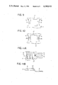
- FIGS. 1 and 2 are sectional views showing the structures of conventional plastic encapsulated power transistors, respectively;
- FIG. 3 is a plan view of a conventional lead frame
- FIG. 4 is a view illustrating the state of plastic encapsulation for forming the plastic encapsulated power transistor of FIG. 2 using the lead frame of FIG. 3;
- FIGS. 5A and 5B are a plan view and a sectional view, respectively, of a lead frame according to one embodiment of the present invention.
- FIGS. 6, 7 and 8 are views illustrating the plastic encapsulation process to the completion of manufacture according to a method for manufacturing the plastic encapsulated semiconductor device of the present invention
- FIGS. 9 and 10 are views showing examples of portions of the strips with small cross-sectional areas respectively.
- FIGS. 11A and 11B are a plan view and a sectional view, respectively, of the main part of a lead frame according to another embodiment of the present invention.
- FIGS. 12, 13 and 14 are plan views of the main part of a lead frame according to still another embodiment of the present invention, respectively.
- FIG. 1 is a sectional view of a conventional power transistor of the plastic encapsulated structure.
- the lower surface of a substrate support 2 on which a transistor element 1 is adhered and which serves as a heat sink is not covered with a plastic encapsulating housing 3 but exposed.
- a through hole 4 is formed for mounting the power transistor on the radiator with a screw.
- Reference numeral 5 denotes a protective plastic portion and reference numeral 6 denotes an external lead.
- the heat radiation effect is guaranteed.
- the insulating plate must be inserted between the radiator and the substrate support when the substrate support is to be mounted on the radiator, resulting in a complicated packaging operation.
- the insulating plate must be properly inserted between the radiator and the substrate support.
- the radiator and the substrate support are to be integrally adhered, they may be misaligned. Thus, electrical insulation cannot be guaranteed. Therefore, as shown in FIG. 2, a plastic encapsulated power transistor is proposed wherein a thin plastic layer 7 is formed on the lower surface of the substrate support 2 and the insulating plate is not required.
- FIG. 3 is a plan view of a lead frame which is conventionally used for packaging the plastic encapsulated power transistor of FIGS. 1 and 2.
- External leads 6, 10 and 11 of the power transistor extend in one direction from a connecting band 9 on which apertures 8 for determining the feed pitch and positioning the substrate support 2 at the time of plastic encapsulation are formed.
- the substrate support 2 is connected to the end of the external lead 6.
- the transistor is packaged in such a manner that the transistor element 1 is adhered, metal wires 12 are connected between the external leads 10 and 11 and electrodes of the transistor element 1 corresponding thereto, and a protective plastic portion 5 is formed.
- a transistor assembly is obtained, using the lead frame as described above.
- This transistor assembly is formed into a plastic encapsulated structure shown in FIG. 2 in the following manner.
- the substrate support 2 of the transistor assembly is floated in a cavity formed between an upper mold 13 and a lower mold 14.
- Plastic 30 is then injected into the cavity.
- the plastic 30 is also filled in the cavity immediately under the lower surface of the substrate support 2.
- the plastic encapsulated semiconductor device of FIG. 2 is manufactured.
- FIGS. 5A and 5B are views illustrating the structure of a lead frame according to the present invention in which FIG. 5A is a plan view thereof and FIG. 5B is a sectional view thereof along the line U--U.
- Two strips 15 and 16 extend from a side of the substrate support 2 which is opposite to the side to which the external lead 6 is connected.
- the strips 15 and 16 are connected to a second connecting band 17.
- Portions 18 and 19 of small cross-sectional areas are formed at the strips 15 and 16, respectively.
- Apertures 20 formed in the second connecting band 17 fit with parts of a mold for alignment in the plastic encapsulation process.
- the thickness of the strips 15 and 16 is smaller than that of the substrate support 2.
- a predetermined step is formed between the rear surfaces of the strips 15 and 16 and the rear surface of the substrate support 2.
- the portions 18 and 19 are thinner than any other portions.
- FIG. 6 is a view illustrating the state of plastic encapsulation of the transistor assembly formed by using the lead frame according to the present invention.
- the plastic 30 is injected into the cavity formed between the upper and lower molds 13 and 14 in the same manner as in the conventional plastic encapsulation.
- the lead frame according to the present invention is used, as shown in the figure, the external lead 6 of the lead frame is clamped by the upper and lower molds 13 and 14 on one side.
- the strips 15 and 16 and the second connecting band 17 are clamped by the upper and lower molds 13 and 14 on the other side.
- Projections (not shown) of the upper mold 13 fit in the apertures 8 formed in the first connecting band 9.
- projections 21 of the upper mold 13 fit in the apertures 20 of the second connecting band 17.
- Reference numeral 22 denotes a projection of the upper mole 13 which forms a through hole for mounting the semiconductor device to a radiator with a screw.
- the substrate support 2 of the lead frame is supported by the external lead 6 and the strips 15 and 16 which are clamped by the upper and lower molds 13 and 14, and thus floats in the cavity of the molds.
- the first and second connecting bands 9 and 17 are clamped by the upper and lower molds 13 and 14, as described above. Further, since the projections of the upper mold 13 are fitted in the apertures formed in the first and second connecting bands 9 and 17, the first and second bands 9 and 17 are not allowed to move horizontally. Thus, the floating condition of the substrate support 2 is properly controlled.
- the cavity formed by the upper and lower molds 13 and 14 terminates at a small cross-sectional area portion 18 (19) of the strip 15 (16). Therefore, the small cross-sectional area portion 18 (19) of the strips 15 (16) extends from the encapsulating housing to the outside after plastic encapsulation is completed. In accordance with the shape of the extending portion of the strips, effects to be described later will be obtained in the cutting operation.
- FIG. 7 is a perspective view illustrating the condition after the plastic encapsulation is completed.
- the plastic encapsulating housing has a thin portion 23 with the through hole 4 for a screw disposed therein and a thick portion 24.
- a step is formed between the thin portion 23 and the thick portion 24.
- the head of the screw mounted in the through hole 4 does not extend higher than the top of the thick portion 24.
- the external leads 6, 10 and 11 are cut from the first connecting band 9 along the line X--X and the strips 15 and 16 are cut at the portions 18 and 19 of small cross-sectional areas along the line Y--Y so as to produce a plastic encapsulated transistor shown in FIG. 8. Since the portions 18 and 19 extending from the thin portion 23 of the plastic encapsulating housing have cross-sectional areas smaller than those of other portions, the strips 15 and 16 are easily cut along the line Y--Y when bent in the vertical direction indicated by an arrow Z--Z. Since the portions 18 and 19 are partially exposed at the end face of the thin portion 23 of the plastic encapsulating housing, the thickness of the strips 15 and 16 is thinner at the end face of the plastic encapsulating housing.
- the substrate support 2 is brought into contact with the plastic material at a relatively long length from the end face of the plastic encapsulating housing to the transistor element 1. Therefore, water or the like may not enter through the cut surface.
- the strips 15 and 16 may be cut by a press machine or the like. However, in order to substantially align the cut surface of the strip with the end face of the plastic encapsulating housing with high precision, it is preferable to bend and cut the strips by brittle fracture under bending stress because cutting by the press machine may damage the encapsulating housing, resulting in poor appearance.
- the cut surfaces of the strips 15 and 16 are exposed at the end face of the plastic encapsulating housing.
- the step is formed between the rear surface of the substrate support 2 and the rear surface of the strips 15 and 16, as shown in FIG. 5, a sufficient space is formed between the cut surfaces and the rear surface of the plastic encapsulating housing which is mounted to the radiator. Short-circuiting does not occur at the cut surfaces of the strips.
- parts of the strips 15 and 16 are made thin in order to reduce the cross-sectional areas of the strips at these parts.
- the thickness of the strips may be kept constant but parts thereof may be narrowed for this purpose.
- holes 25 and 26 may be formed in the strips 15 and 16, respectively, to substantially partially reduce the width of the strips 15 and 16.
- the plastic for plastic capsulation used according to the method of the present invention preferably has high thermal conductivity.
- the thickness of the plastic layer immediately under the substrate support is preferably 0.3 to 0.5 mm in consideration of heat radiation and electrical insulation. With the thickness within this range, better results are obtained.
- a thin layer of plastic 30 is formed on the rear surface of the substrate support, to the upper surface of which the transistor element 1 is adhered.
- the layer of plastic 30 has thermal conductivity lower than that of the substrate support 2 comprising a metal plate. Therefore, the plastic layer on the rear surface of the substrate support 2 must be as thin as possible and must comprise a plastic of very high thermal conductivity. In consideration of this, although a very thin plastic layer is formed on the rear surface of the substrate support 2, the plastic film may peel off the substrate support 2 due to heat shrinkage therebetween, thus resulting in changes of heat dissipation characteristic over time, degradation of resistance to humidity, degradation of mechanical strength, and degradation of electrical insulation.
- the present invention provides a plastic encapsulated semiconductor device with an insulation structure which eliminates the above problem.
- the characteristic feature of the present invention resides in that grooves or bores are formed in at least part of a surface opposing the semiconductor substrate adhered surface of the substrate support connected to one of the external leads extending in the same direction from the connecting band.
- FIG. 11A is a plan view of the main part of a lead frame for a plastic encapsulated semiconductor device according to another embodiment of the present invention
- FIG. 11B is a sectional view thereof along the line W--W of FIG. 11A.
- a plurality of grooves 27 are formed perpendicularly to the direction indicated by an arrow T. The width, depth and pitch of these grooves are not limited but may be changed as needed.
- An increase in the surface area is proportional to the total area of inner walls of the grooves. Assume that the number of grooves is defined as n, the length of each groove is defined as l, and the depth of the grooves is defined as d.
- FIGS. 12, 13 and 14 show other examples of three-dimensionally patterned surface of the substrate support 2, respectively.
- a plurality of grooves 27 are formed in a lattice shape on the rear surface of the substrate support 2 in FIG. 12; a plurality of grooves 27 parallel to the direction indicated by the arrow T are formed thereon in FIG. 13; and a plurality of bores each of which has predetermined diameter and depth are formed thereon in FIG. 14.
- the plastic is injected in the molds in the direction indicated by the arrow T. If the three-dimensional patterning process as shown in FIG. 13 is performed, the flow of the plastic in the molds is very smooth, so voids or the like are easily eliminated, resulting in good appearance and the improvement of electrical insulation of the device.
- a plastic encapsulated semiconductor device which has a thin plastic layer immediately under the substrate support which also serves as the heat sink is manufactured with high precision according to the present invention.
Abstract
A method for manufacturing a plastic encapsulated semiconductor device is provided which comprises the steps of: clamping by upper and lower molds at least external leads and strips of a semiconductor device assembly formed using a lead frame which has a first connecting band connected to the external leads extending from one side of a substrate support further used as a heat sink, and a second connecting band connected to the strips having portions of small cross-sectional areas and of a predetermined length and extending from the other side of the substrate support, the cross sections being perpendicular to an extending direction of the strips, so that the substrate support may float in a cavity formed by the upper and lower molds and parts of the portions of small cross-sectional areas may be disposed in the cavity and the remaining parts thereof may be disposed between the upper and lower molds; injecting a plastic into the cavity; and cutting the portions of small cross-sectional areas of the strips which extend outside a plastic encapsulating housing along the end face of the plastic encapsulating housing and cutting a connecting portion between the external leads and the first connecting band. Also provided is a lead frame having the strips as decribed above. A plastic layer of desired thickness can be formed on the rear surface of the substrate support. Cutting of the strips from the plastic encapsulating housing is easy and reliable.
Description
This is a division of application Ser. No. 367,809, filed Apr. 13, 1982, now U.S. Pat. No. 4,451,973.
I. Field of the Invention
The present invention relates to a method for manufacturing a plastic encapsulated semiconductor device which can be used with relatively large power and a lead frame therefor.
II. Description of the Prior Art
Plastic encapsulated semiconductor devices are superior to metal encapsulated semiconductor devices in ease in mass production and manufacturing costs. However, the plastic encapsulated semiconductor devices are inferior to the metal encapsulated semiconductor devices in radiation of heat when they are operated. Plastic encapsulation of semiconductor devices has recently been developed. A high power transistor manufactured by plastic encapsulation has been proposed. In this case, sufficient consideration is taken to allow the radiation of heat.
In a transistor adhered on a metal substrate support and encapsulated by plastic, for example, the lower surface of the substrate support is not covered with plastic but exposed. The substrate support is mounted on a radiator to radiate heat. However, in this case, the substrate support must be electrically insulated from the radiator. The packaging operation of the semiconductor device on the radiator through an insulating plate is complicated and cumbersome.
On the other hand, a plastic encapsulated power transistor is proposed wherein a thin plastic layer is formed on the lower surface of the substrate support during plastic encapsulation and an insulating plate is not required for mounting the power transistor on the radiator. However, in this case, at the time of plastic encapsulation, only the side of the lead frame from which extend the external lead is clamped by the upper and lower molds with a transistor assembly which has the external lead on one side. Plastic is injected while the substrate support is floating in a cavity defined by the molds. Thus, the substrate support may be bent in the cavity due to the injection pressure of the plastic. As a result, it is very difficult to encapsulate in plastic while keeping the substrate support in a proper position, thus, resulting in non-uniformity in the thickness of the plastic layer on the lower surface of the substrate support and degrading radiation characteristics.
It is an object of the present invention to provide a method for manufacturing a plastic encapsulated semiconductor device and a lead frame therefor wherein, in manufacturing a plastic encapsulated semiconductor device of a structure which has a thin plastic layer on one surface of a substrate support which supports a semiconductor substrate and also serves as a heat sink, to the other surface of which the semiconductor substrate is adhered, the thickness of the thin plastic layer is uniformly formed and with high precision.
In order to achieve the above object of the present invention, there is provided a method for manufacturing a plastic encapsulated semiconductor device and a lead frame therefor wherein a semiconductor device assembly is formed, using a lead frame an external lead of which extends to one side of a substrate support and strips of which extend to the other end of the substrate support, said strips each having a portion of cross-sectional area are made small for a predetermined length, the cross sections being perpendicular to the extending direction of said strips; the external lead and strips are clamped by upper and lower molds so as to float the substrate support in a cavity of the molds and to position part of the portion of each of the strips with small cross-sectional area in the cavity of the molds and the remaining part of the portion of each of the strips between the molds for plastic encapsulation, and a connecting portion between a first connecting band and the external lead and the portion of each of the strips with small cross-sectional area extending from a plastic encapsulating housing to the outside are cut.
The substrate support is, therefore, supported properly at the time of plastic encapsulation. The substrate support may not be bent due to injection pressure of the plastic, so that a plastic layer is uniformly formed on the rear surface of the substrate support with high precision. Further, the portions of the strips with small cross-sectional areas are easily cut without damaging the encapsulating housing.
The above and other objects and features of the present invention will become apparent from the following detailed description of the preferred embodiments when taken in conjunction with reference to the accompanying drawings.
FIGS. 1 and 2 are sectional views showing the structures of conventional plastic encapsulated power transistors, respectively;
FIG. 3 is a plan view of a conventional lead frame;
FIG. 4 is a view illustrating the state of plastic encapsulation for forming the plastic encapsulated power transistor of FIG. 2 using the lead frame of FIG. 3;
FIGS. 5A and 5B are a plan view and a sectional view, respectively, of a lead frame according to one embodiment of the present invention;
FIGS. 6, 7 and 8 are views illustrating the plastic encapsulation process to the completion of manufacture according to a method for manufacturing the plastic encapsulated semiconductor device of the present invention;
FIGS. 9 and 10 are views showing examples of portions of the strips with small cross-sectional areas respectively;
FIGS. 11A and 11B are a plan view and a sectional view, respectively, of the main part of a lead frame according to another embodiment of the present invention; and
FIGS. 12, 13 and 14 are plan views of the main part of a lead frame according to still another embodiment of the present invention, respectively.
FIG. 1 is a sectional view of a conventional power transistor of the plastic encapsulated structure. The lower surface of a substrate support 2 on which a transistor element 1 is adhered and which serves as a heat sink is not covered with a plastic encapsulating housing 3 but exposed. A through hole 4 is formed for mounting the power transistor on the radiator with a screw. Reference numeral 5 denotes a protective plastic portion and reference numeral 6 denotes an external lead. When the plastic encapsulated power transistor with the above structure is to be mounted on the radiator (not shown), the exposed lower surface of the substrate support 2 must be thermally coupled with the radiator but must be electrically insulated therefrom. This electrical insulation may be performed by insertion of an insulating plate such as a mica plate.
With the above structure, the heat radiation effect is guaranteed. However, the insulating plate must be inserted between the radiator and the substrate support when the substrate support is to be mounted on the radiator, resulting in a complicated packaging operation. Furthermore, the insulating plate must be properly inserted between the radiator and the substrate support. When the insulating plate, the radiator and the substrate support are to be integrally adhered, they may be misaligned. Thus, electrical insulation cannot be guaranteed. Therefore, as shown in FIG. 2, a plastic encapsulated power transistor is proposed wherein a thin plastic layer 7 is formed on the lower surface of the substrate support 2 and the insulating plate is not required.
FIG. 3 is a plan view of a lead frame which is conventionally used for packaging the plastic encapsulated power transistor of FIGS. 1 and 2. External leads 6, 10 and 11 of the power transistor extend in one direction from a connecting band 9 on which apertures 8 for determining the feed pitch and positioning the substrate support 2 at the time of plastic encapsulation are formed. As shown in FIG. 4, the substrate support 2 is connected to the end of the external lead 6. As shown in the leftmost transistor, the transistor is packaged in such a manner that the transistor element 1 is adhered, metal wires 12 are connected between the external leads 10 and 11 and electrodes of the transistor element 1 corresponding thereto, and a protective plastic portion 5 is formed.
A transistor assembly is obtained, using the lead frame as described above. This transistor assembly is formed into a plastic encapsulated structure shown in FIG. 2 in the following manner. As shown in FIG. 4, the substrate support 2 of the transistor assembly is floated in a cavity formed between an upper mold 13 and a lower mold 14. Plastic 30 is then injected into the cavity. The plastic 30 is also filled in the cavity immediately under the lower surface of the substrate support 2. Thus, the plastic encapsulated semiconductor device of FIG. 2 is manufactured.
As is apparent from FIG. 4, when the plastic encapsulated structure of FIG. 2 is to be obtained by using the lead frame of FIG. 3, plastic is injected into the cavity while only the side on which the external leads are formed is clamped between the upper and lower molds. The substrate support 2 may be bent within the cavity due to the injection pressure of the plastic. Therefore, it is very difficult to dispose the substrate support 2 in a proper position. If the substrate support 2 is bent, the uniform thickness of the thin plastic layer 7 is not obtained. Further, this non-uniformity in thickness directly results in degradation of radiation characteristics.
FIGS. 5A and 5B are views illustrating the structure of a lead frame according to the present invention in which FIG. 5A is a plan view thereof and FIG. 5B is a sectional view thereof along the line U--U.
Two strips 15 and 16 extend from a side of the substrate support 2 which is opposite to the side to which the external lead 6 is connected. The strips 15 and 16 are connected to a second connecting band 17. Portions 18 and 19 of small cross-sectional areas are formed at the strips 15 and 16, respectively. Apertures 20 formed in the second connecting band 17 fit with parts of a mold for alignment in the plastic encapsulation process. As shown in FIG. 5B, the thickness of the strips 15 and 16 is smaller than that of the substrate support 2. A predetermined step is formed between the rear surfaces of the strips 15 and 16 and the rear surface of the substrate support 2. Thus, the portions 18 and 19 are thinner than any other portions.
FIG. 6 is a view illustrating the state of plastic encapsulation of the transistor assembly formed by using the lead frame according to the present invention. The plastic 30 is injected into the cavity formed between the upper and lower molds 13 and 14 in the same manner as in the conventional plastic encapsulation. However, when the lead frame according to the present invention is used, as shown in the figure, the external lead 6 of the lead frame is clamped by the upper and lower molds 13 and 14 on one side. At the same time, the strips 15 and 16 and the second connecting band 17 are clamped by the upper and lower molds 13 and 14 on the other side. Projections (not shown) of the upper mold 13 fit in the apertures 8 formed in the first connecting band 9. Simultaneously, projections 21 of the upper mold 13 fit in the apertures 20 of the second connecting band 17. Reference numeral 22 denotes a projection of the upper mole 13 which forms a through hole for mounting the semiconductor device to a radiator with a screw.
According to the present invention, the substrate support 2 of the lead frame is supported by the external lead 6 and the strips 15 and 16 which are clamped by the upper and lower molds 13 and 14, and thus floats in the cavity of the molds. The first and second connecting bands 9 and 17 are clamped by the upper and lower molds 13 and 14, as described above. Further, since the projections of the upper mold 13 are fitted in the apertures formed in the first and second connecting bands 9 and 17, the first and second bands 9 and 17 are not allowed to move horizontally. Thus, the floating condition of the substrate support 2 is properly controlled.
As is apparent from FIG. 6, the cavity formed by the upper and lower molds 13 and 14 terminates at a small cross-sectional area portion 18 (19) of the strip 15 (16). Therefore, the small cross-sectional area portion 18 (19) of the strips 15 (16) extends from the encapsulating housing to the outside after plastic encapsulation is completed. In accordance with the shape of the extending portion of the strips, effects to be described later will be obtained in the cutting operation.
FIG. 7 is a perspective view illustrating the condition after the plastic encapsulation is completed. As shown in the figure, the plastic encapsulating housing has a thin portion 23 with the through hole 4 for a screw disposed therein and a thick portion 24. A step is formed between the thin portion 23 and the thick portion 24. The head of the screw mounted in the through hole 4 does not extend higher than the top of the thick portion 24.
The external leads 6, 10 and 11 are cut from the first connecting band 9 along the line X--X and the strips 15 and 16 are cut at the portions 18 and 19 of small cross-sectional areas along the line Y--Y so as to produce a plastic encapsulated transistor shown in FIG. 8. Since the portions 18 and 19 extending from the thin portion 23 of the plastic encapsulating housing have cross-sectional areas smaller than those of other portions, the strips 15 and 16 are easily cut along the line Y--Y when bent in the vertical direction indicated by an arrow Z--Z. Since the portions 18 and 19 are partially exposed at the end face of the thin portion 23 of the plastic encapsulating housing, the thickness of the strips 15 and 16 is thinner at the end face of the plastic encapsulating housing. Further, since a step is formed between the portion 18 and the strip 15 and between the portion 19 and the strip 16, the substrate support 2 is brought into contact with the plastic material at a relatively long length from the end face of the plastic encapsulating housing to the transistor element 1. Therefore, water or the like may not enter through the cut surface. The strips 15 and 16 may be cut by a press machine or the like. However, in order to substantially align the cut surface of the strip with the end face of the plastic encapsulating housing with high precision, it is preferable to bend and cut the strips by brittle fracture under bending stress because cutting by the press machine may damage the encapsulating housing, resulting in poor appearance.
In the transistor manufactured according to the method of the present invention, the cut surfaces of the strips 15 and 16 are exposed at the end face of the plastic encapsulating housing. However, since the step is formed between the rear surface of the substrate support 2 and the rear surface of the strips 15 and 16, as shown in FIG. 5, a sufficient space is formed between the cut surfaces and the rear surface of the plastic encapsulating housing which is mounted to the radiator. Short-circuiting does not occur at the cut surfaces of the strips.
In the above embodiment, parts of the strips 15 and 16 are made thin in order to reduce the cross-sectional areas of the strips at these parts. However, as shown in FIG. 9, the thickness of the strips may be kept constant but parts thereof may be narrowed for this purpose. Alternatively, as shown in FIG. 10, holes 25 and 26 may be formed in the strips 15 and 16, respectively, to substantially partially reduce the width of the strips 15 and 16. The plastic for plastic capsulation used according to the method of the present invention preferably has high thermal conductivity. The thickness of the plastic layer immediately under the substrate support is preferably 0.3 to 0.5 mm in consideration of heat radiation and electrical insulation. With the thickness within this range, better results are obtained.
In the plastic encapsulated semiconductor device with an insulation structure formed by the process described above, as is also apparent from FIG. 6, a thin layer of plastic 30 is formed on the rear surface of the substrate support, to the upper surface of which the transistor element 1 is adhered. The layer of plastic 30 has thermal conductivity lower than that of the substrate support 2 comprising a metal plate. Therefore, the plastic layer on the rear surface of the substrate support 2 must be as thin as possible and must comprise a plastic of very high thermal conductivity. In consideration of this, although a very thin plastic layer is formed on the rear surface of the substrate support 2, the plastic film may peel off the substrate support 2 due to heat shrinkage therebetween, thus resulting in changes of heat dissipation characteristic over time, degradation of resistance to humidity, degradation of mechanical strength, and degradation of electrical insulation.
The present invention provides a plastic encapsulated semiconductor device with an insulation structure which eliminates the above problem. The characteristic feature of the present invention resides in that grooves or bores are formed in at least part of a surface opposing the semiconductor substrate adhered surface of the substrate support connected to one of the external leads extending in the same direction from the connecting band.
The above feature will be described in detail with reference to the accompanying drawings. FIG. 11A is a plan view of the main part of a lead frame for a plastic encapsulated semiconductor device according to another embodiment of the present invention, and FIG. 11B is a sectional view thereof along the line W--W of FIG. 11A. A plurality of grooves 27 are formed perpendicularly to the direction indicated by an arrow T. The width, depth and pitch of these grooves are not limited but may be changed as needed. When a thin plastic layer is formed on a three-dimensional surface, the surface area of the substrate support which is brought into contact with the plastic layer is increased. Therefore, heat dissipation characteristics are, of course, improved and the plastic layer is strongly adhered to the substrate support 2. Thus, the plastic layer does not peel off the substrate support 2, although the layer tends to peel off the flat surface of the substrate support 2.
An increase in the surface area is proportional to the total area of inner walls of the grooves. Assume that the number of grooves is defined as n, the length of each groove is defined as l, and the depth of the grooves is defined as d. An increase ΔS of the surface area is given by the relation: ΔS=2nld. For example, assume that fifteen parallel grooves of 200 μm width and 100 μm depth are formed in a substrate support of 15 mm length and 10 mm width. The surface area is calculated as 150+(2×15×10×0.1)=180 mm2, whereas the surface area of the substrate support without grooves is calculated as 150 mm2. Thus, an increase ΔS of 20% is obtained.
FIGS. 12, 13 and 14 show other examples of three-dimensionally patterned surface of the substrate support 2, respectively. A plurality of grooves 27 are formed in a lattice shape on the rear surface of the substrate support 2 in FIG. 12; a plurality of grooves 27 parallel to the direction indicated by the arrow T are formed thereon in FIG. 13; and a plurality of bores each of which has predetermined diameter and depth are formed thereon in FIG. 14. The same effects as described above are obtained in all modifications of the grooves 27. Further, the plastic is injected in the molds in the direction indicated by the arrow T. If the three-dimensional patterning process as shown in FIG. 13 is performed, the flow of the plastic in the molds is very smooth, so voids or the like are easily eliminated, resulting in good appearance and the improvement of electrical insulation of the device.
As is apparent from the above description, a plastic encapsulated semiconductor device which has a thin plastic layer immediately under the substrate support which also serves as the heat sink is manufactured with high precision according to the present invention.
Claims (10)
1. A lead frame comprising a first connecting band, a plurality of external leads extending in one direction from said first connecting band, a substrate support having a rear surface and which serves as a heat sink connected at one side thereof to a free end of one of said external leads, a plurality of support strips, each having a portion of small cross-sectional area and being of a predetermined length and extending in a lengthwise direction between portions of larger cross-sectional areas of the respective strip, the cross sections of said portions of small cross-sectional areas being taken perpendicular to said lengthwise direction of said strips, and one end of said strip is connected to another side of said substrate support opposite to the one side connected to said external leads, and a second connecting band extending parallel to said first connecting band with said substrate support disposed therebetween, and connected to opposite ends of said strips, said strips having a smaller thickness than said substrate support and rear surfaces of said strips being at a higher level than the rear surface of said substrate support.
2. A lead frame according to claim 1, wherein two strips are connected to each said substrate support.
3. A lead frame according to claim 1, wherein said portions of small cross-sectional areas of said strips have narrowed portions, respectively, to reduce the cross-sectional areas of said portions of said strips.
4. A lead frame according to claim 1, wherein said strips have apertures, respectively, to substantially reduce the cross-sectional areas of said portions of small cross-sectional areas of said strips.
5. A lead frame according to claim 1, wherein a plurality of apertures are formed in each of said first and second connecting bands at an equal pitch.
6. A lead frame according to claim 1, wherein a three-dimensional pattern of one of a groove shape and a bore shape is formed on at least part of one surface of said substrate support and an opposite surface of which supports a semiconductor substrate.
7. A lead frame according to claim 6, wherein said three-dimensional pattern has grooves extending perpendicular to a longitudinal direction of said substrate support.
8. A lead frame according to claim 6, wherein said three-dimensional pattern has grooves in a lattice form.
9. A lead frame according to claim 6, wherein said three-dimensional pattern has grooves extending parallel to a longitudinal direction of said substrate support.
10. A lead frame according to claim 6, wherein said three-dimensional pattern has a number of bores.
Applications Claiming Priority (4)
| Application Number | Priority Date | Filing Date | Title |
|---|---|---|---|
| JP6489381A JPS57178352A (en) | 1981-04-28 | 1981-04-28 | Manufacture of resin sealing type semiconductor device and lead frame employed thereon |
| JP56-64893 | 1981-04-28 | ||
| JP56-64307 | 1981-04-30 | ||
| JP6430781A JPS5710325A (en) | 1980-05-16 | 1981-04-30 | Device for simultaneously and continuously supplying powdered solid or liquid into treating machine |
Related Parent Applications (1)
| Application Number | Title | Priority Date | Filing Date |
|---|---|---|---|
| US06/367,809 Division US4451973A (en) | 1981-04-28 | 1982-04-13 | Method for manufacturing a plastic encapsulated semiconductor device and a lead frame therefor |
Publications (1)
| Publication Number | Publication Date |
|---|---|
| US4589010A true US4589010A (en) | 1986-05-13 |
Family
ID=26405427
Family Applications (2)
| Application Number | Title | Priority Date | Filing Date |
|---|---|---|---|
| US06/367,809 Expired - Lifetime US4451973A (en) | 1981-04-28 | 1982-04-13 | Method for manufacturing a plastic encapsulated semiconductor device and a lead frame therefor |
| US06/581,251 Expired - Lifetime US4589010A (en) | 1981-04-28 | 1984-02-17 | Method for manufacturing a plastic encapsulated semiconductor device and a lead frame therefor |
Family Applications Before (1)
| Application Number | Title | Priority Date | Filing Date |
|---|---|---|---|
| US06/367,809 Expired - Lifetime US4451973A (en) | 1981-04-28 | 1982-04-13 | Method for manufacturing a plastic encapsulated semiconductor device and a lead frame therefor |
Country Status (4)
| Country | Link |
|---|---|
| US (2) | US4451973A (en) |
| EP (1) | EP0063811B1 (en) |
| CA (1) | CA1200623A (en) |
| DE (2) | DE63811T1 (en) |
Cited By (23)
| Publication number | Priority date | Publication date | Assignee | Title |
|---|---|---|---|---|
| US4857989A (en) * | 1986-09-04 | 1989-08-15 | Mitsubishi Denki Kabushiki Kaisha | Semiconductor device |
| US4862246A (en) * | 1984-09-26 | 1989-08-29 | Hitachi, Ltd. | Semiconductor device lead frame with etched through holes |
| US4942452A (en) * | 1987-02-25 | 1990-07-17 | Hitachi, Ltd. | Lead frame and semiconductor device |
| US4952999A (en) * | 1988-04-26 | 1990-08-28 | National Semiconductor Corporation | Method and apparatus for reducing die stress |
| US4991002A (en) * | 1990-02-14 | 1991-02-05 | Motorola Inc. | Modular power device assembly |
| US5019893A (en) * | 1990-03-01 | 1991-05-28 | Motorola, Inc. | Single package, multiple, electrically isolated power semiconductor devices |
| US5083368A (en) * | 1990-02-14 | 1992-01-28 | Motorola Inc. | Method of forming modular power device assembly |
| US5122858A (en) * | 1990-09-10 | 1992-06-16 | Olin Corporation | Lead frame having polymer coated surface portions |
| US5138428A (en) * | 1989-05-31 | 1992-08-11 | Siemens Aktiengesellschaft | Connection of a semiconductor component to a metal carrier |
| US5252944A (en) * | 1991-09-12 | 1993-10-12 | Caddock Electronics, Inc. | Film-type electrical resistor combination |
| US5367196A (en) * | 1992-09-17 | 1994-11-22 | Olin Corporation | Molded plastic semiconductor package including an aluminum alloy heat spreader |
| US5581118A (en) * | 1994-05-31 | 1996-12-03 | Motorola, Inc. | Electronic surface mount device |
| US5608267A (en) * | 1992-09-17 | 1997-03-04 | Olin Corporation | Molded plastic semiconductor package including heat spreader |
| DE19702104A1 (en) * | 1996-01-22 | 1997-07-24 | Murata Manufacturing Co | Electronic component with protective insulation |
| US5748658A (en) * | 1993-10-22 | 1998-05-05 | Matsushita Electric Industrial Co., Ltd. | Semiconductor laser device and optical pickup head |
| US6373126B1 (en) * | 2000-04-26 | 2002-04-16 | Advanced Micro Devices, Inc. | Method for reducing IC package delamination by use of internal baffles |
| USRE37690E1 (en) * | 1987-02-25 | 2002-05-07 | Hitachi, Ltd. | Lead frame and semiconductor device |
| US6469907B1 (en) | 2000-10-23 | 2002-10-22 | Team Pacific, Corporation | Packaging for power and other circuitry |
| US20030042626A1 (en) * | 2001-08-30 | 2003-03-06 | Howarth James J. | Method of ball grid array (BGA) alignment, method of testing, alignment apparatus and semiconductor device assembly |
| US6836003B2 (en) | 1997-09-15 | 2004-12-28 | Micron Technology, Inc. | Integrated circuit package alignment feature |
| US20070126445A1 (en) * | 2005-11-30 | 2007-06-07 | Micron Technology, Inc. | Integrated circuit package testing devices and methods of making and using same |
| DE10221085B4 (en) * | 2002-05-11 | 2012-07-26 | Robert Bosch Gmbh | Assembly having a connection device for contacting a semiconductor device and manufacturing method |
| US20190097524A1 (en) * | 2011-09-13 | 2019-03-28 | Fsp Technology Inc. | Circuit having snubber circuit in power supply device |
Families Citing this family (61)
| Publication number | Priority date | Publication date | Assignee | Title |
|---|---|---|---|---|
| JPS57147260A (en) * | 1981-03-05 | 1982-09-11 | Matsushita Electronics Corp | Manufacture of resin-sealed semiconductor device and lead frame used therefor |
| US4641418A (en) * | 1982-08-30 | 1987-02-10 | International Rectifier Corporation | Molding process for semiconductor devices and lead frame structure therefor |
| JPS59130449A (en) * | 1983-01-17 | 1984-07-27 | Nec Corp | Insulation type semiconductor element |
| JPS59135753A (en) * | 1983-01-25 | 1984-08-04 | Toshiba Corp | Semiconductor device and manufacture thereof |
| IT1212780B (en) * | 1983-10-21 | 1989-11-30 | Ates Componenti Elettron | METAL AND RESIN CONTAINER FOR A SEMICONDUCTOR DEVICE SUITABLE FOR FASTENING TO A NOT PERFECTLY FLAT HEATER AND PROCESS FOR ITS MANUFACTURE. |
| JPS60186044A (en) * | 1983-12-12 | 1985-09-21 | テキサス インスツルメンツ インコ−ポレイテツド | Integrated circuit device |
| JPS60128646A (en) * | 1983-12-16 | 1985-07-09 | Hitachi Ltd | Semiconductor device and lead frame used for manufacturing the same device |
| IT1213139B (en) * | 1984-02-17 | 1989-12-14 | Ates Componenti Elettron | SINGLE-IN-LINE INTEGRATED ELECTRONIC COMPONENT AND PROCEDURE FOR ITS MANUFACTURE. |
| JPS60176259A (en) * | 1984-02-22 | 1985-09-10 | Toshiba Corp | Manufacture of resin seal type semiconductor device |
| IT1180514B (en) * | 1984-07-27 | 1987-09-23 | Arcotroniks Italia Spa | PROCEDURE FOR THE CREATION OF PROTECTIVE ENCLOSURES IN WHICH CORRESPONDING ELECTRONIC ELECTRONIC COMPONENTS ARE ANNEXED |
| US5098630A (en) * | 1985-03-08 | 1992-03-24 | Olympus Optical Co., Ltd. | Method of molding a solid state image pickup device |
| EP0206771B1 (en) * | 1985-06-20 | 1992-03-11 | Kabushiki Kaisha Toshiba | Packaged semiconductor device |
| JPH0652732B2 (en) * | 1985-08-14 | 1994-07-06 | 三菱電機株式会社 | Method for forming passivation film |
| US4721453A (en) * | 1986-03-05 | 1988-01-26 | Gte Communication Systems Corporation | Apparatus for encapsulating semiconductors |
| EP0257681A3 (en) * | 1986-08-27 | 1990-02-07 | STMicroelectronics S.r.l. | Method for manufacturing plastic encapsulated semiconductor devices and devices obtained thereby |
| IT1214254B (en) * | 1987-09-23 | 1990-01-10 | Sgs Microelettonica S P A | SEMICONDUCTOR DEVICE IN PLASTIC OR CERAMIC CONTAINER WITH "CHIPS" FIXED ON BOTH SIDES OF THE CENTRAL ISLAND OF THE "FRAME". |
| US4904539A (en) * | 1987-09-30 | 1990-02-27 | Amp Incorporated | Continuous strip of electrical component assemblies and method of making same |
| JPH01179332A (en) * | 1987-12-31 | 1989-07-17 | Sanken Electric Co Ltd | Manufacture of plastic-sealed electronic device |
| US5049055A (en) * | 1987-12-31 | 1991-09-17 | Sanken Electric Co., Ltd. | Mold assembly |
| US5133921A (en) * | 1987-12-31 | 1992-07-28 | Sanken Electric Co., Ltd. | Method for manufacturing plastic encapsulated electronic semiconductor devices |
| US5049976A (en) * | 1989-01-10 | 1991-09-17 | National Semiconductor Corporation | Stress reduction package and process |
| US4908935A (en) * | 1989-03-22 | 1990-03-20 | American Telephone And Telegraph Company, At&T Bell Laboratories | Method for fabricating electronic devices |
| JPH0419114A (en) * | 1990-05-15 | 1992-01-23 | Mitsubishi Electric Corp | Manufacture of insert electrode molding |
| US5367766A (en) * | 1990-08-01 | 1994-11-29 | Staktek Corporation | Ultra high density integrated circuit packages method |
| US5377077A (en) * | 1990-08-01 | 1994-12-27 | Staktek Corporation | Ultra high density integrated circuit packages method and apparatus |
| US5446620A (en) * | 1990-08-01 | 1995-08-29 | Staktek Corporation | Ultra high density integrated circuit packages |
| WO1992003035A1 (en) * | 1990-08-01 | 1992-02-20 | Staktek Corporation | Ultra high density integrated circuit packages, method and apparatus |
| US5475920A (en) * | 1990-08-01 | 1995-12-19 | Burns; Carmen D. | Method of assembling ultra high density integrated circuit packages |
| IT1247649B (en) * | 1990-10-31 | 1994-12-28 | Sgs Thomson Microelectronics | RESIN ENCAPSULATION PROCEDURE OF A POWER SEMICONDUCTOR DEVICE MOUNTED ON A HEAT SINK REMOVING THE WIRES FROM THE HEAT SINK THROUGH THE ACTION OF THE COUNTER-MOLD WHEN THE MOLD IS CLOSED |
| US5448450A (en) * | 1991-08-15 | 1995-09-05 | Staktek Corporation | Lead-on-chip integrated circuit apparatus |
| MX9205128A (en) * | 1991-09-30 | 1993-04-01 | Motorola Inc | METHOD FOR PROCESSING A SEMICONDUCTOR INTEGRATED CIRCUIT BLOCK. |
| US5804870A (en) * | 1992-06-26 | 1998-09-08 | Staktek Corporation | Hermetically sealed integrated circuit lead-on package configuration |
| US5702985A (en) * | 1992-06-26 | 1997-12-30 | Staktek Corporation | Hermetically sealed ceramic integrated circuit heat dissipating package fabrication method |
| EP0665591A1 (en) * | 1992-11-06 | 1995-08-02 | Motorola, Inc. | Method for forming a power circuit package |
| US5484959A (en) * | 1992-12-11 | 1996-01-16 | Staktek Corporation | High density lead-on-package fabrication method and apparatus |
| US6205654B1 (en) | 1992-12-11 | 2001-03-27 | Staktek Group L.P. | Method of manufacturing a surface mount package |
| JP2927660B2 (en) * | 1993-01-25 | 1999-07-28 | シャープ株式会社 | Method for manufacturing resin-encapsulated semiconductor device |
| US5644161A (en) * | 1993-03-29 | 1997-07-01 | Staktek Corporation | Ultra-high density warp-resistant memory module |
| US5801437A (en) * | 1993-03-29 | 1998-09-01 | Staktek Corporation | Three-dimensional warp-resistant integrated circuit module method and apparatus |
| US5369056A (en) * | 1993-03-29 | 1994-11-29 | Staktek Corporation | Warp-resistent ultra-thin integrated circuit package fabrication method |
| US5506753A (en) * | 1994-09-26 | 1996-04-09 | International Business Machines Corporation | Method and apparatus for a stress relieved electronic module |
| US6025642A (en) * | 1995-08-17 | 2000-02-15 | Staktek Corporation | Ultra high density integrated circuit packages |
| US5886400A (en) * | 1995-08-31 | 1999-03-23 | Motorola, Inc. | Semiconductor device having an insulating layer and method for making |
| JP3345241B2 (en) * | 1995-11-30 | 2002-11-18 | 三菱電機株式会社 | Semiconductor device |
| US5938038A (en) | 1996-08-02 | 1999-08-17 | Dial Tool Industries, Inc. | Parts carrier strip and apparatus for assembling parts in such a strip |
| US5945732A (en) | 1997-03-12 | 1999-08-31 | Staktek Corporation | Apparatus and method of manufacturing a warp resistant thermally conductive integrated circuit package |
| US6252772B1 (en) * | 1999-02-10 | 2001-06-26 | Micron Technology, Inc. | Removable heat sink bumpers on a quad flat package |
| KR200168178Y1 (en) * | 1999-08-27 | 2000-02-15 | 광전자주식회사 | Power package lead frame |
| US6572387B2 (en) | 1999-09-24 | 2003-06-03 | Staktek Group, L.P. | Flexible circuit connector for stacked chip module |
| US6608763B1 (en) | 2000-09-15 | 2003-08-19 | Staktek Group L.P. | Stacking system and method |
| US6462408B1 (en) | 2001-03-27 | 2002-10-08 | Staktek Group, L.P. | Contact member stacking system and method |
| DE10247610A1 (en) * | 2002-10-11 | 2004-04-29 | Micronas Gmbh | Electronic component with a leadframe |
| US20040113240A1 (en) * | 2002-10-11 | 2004-06-17 | Wolfgang Hauser | An electronic component with a leadframe |
| US7008825B1 (en) * | 2003-05-27 | 2006-03-07 | Amkor Technology, Inc. | Leadframe strip having enhanced testability |
| US7342297B1 (en) | 2004-04-22 | 2008-03-11 | National Semiconductor Corporation | Sawn power package |
| US7005728B1 (en) | 2004-06-03 | 2006-02-28 | National Semiconductor Corporation | Lead configuration for inline packages |
| US8334583B2 (en) * | 2005-07-20 | 2012-12-18 | Infineon Technologies Ag | Leadframe strip and mold apparatus for an electronic component and method of encapsulating an electronic component |
| US7602054B2 (en) * | 2005-10-05 | 2009-10-13 | Semiconductor Components Industries, L.L.C. | Method of forming a molded array package device having an exposed tab and structure |
| US7588999B2 (en) * | 2005-10-28 | 2009-09-15 | Semiconductor Components Industries, Llc | Method of forming a leaded molded array package |
| ITTO20070489A1 (en) * | 2007-07-05 | 2009-01-06 | St Microelectronics Srl | PROCEDURE AND MANUFACTURING SYSTEM OF AN ENCAPSULATED SEMICONDUCTOR DEVICE |
| NL2010379C2 (en) * | 2013-03-01 | 2014-09-03 | Besi Netherlands B V | TEMPLATE, CARRIER WITH ELECTRONIC COMPONENTS TO BE COVERED, CARRIER WITH ELECTRONIC COMPONENTS COVERED, SAVED COVERED ELECTRONIC COMPONENT AND METHOD OF COVERING ELECTRONIC COMPONENTS. |
Citations (13)
| Publication number | Priority date | Publication date | Assignee | Title |
|---|---|---|---|---|
| US2965819A (en) * | 1958-08-07 | 1960-12-20 | Rosenbaum Jacob | Heat dissipating electronic mounting apparatus |
| GB877674A (en) * | 1959-09-30 | 1961-09-20 | Gerhard Muller | Improvements in or relating to co-operating electrical contacts engageable by relative sliding displacement |
| US3431092A (en) * | 1965-10-22 | 1969-03-04 | Motorola Inc | Lead frame members for semiconductor devices |
| US3881241A (en) * | 1970-09-28 | 1975-05-06 | Denki Onkyo Company Ltd | Galvano-magneto effect device |
| US3930114A (en) * | 1975-03-17 | 1975-12-30 | Nat Semiconductor Corp | Integrated circuit package utilizing novel heat sink structure |
| JPS5238885A (en) * | 1975-09-22 | 1977-03-25 | Nec Home Electronics Ltd | Method for production of semiconductor device |
| US4250347A (en) * | 1977-05-05 | 1981-02-10 | Fierkens Richardus H | Method of encapsulating microelectronic elements |
| JPS5655065A (en) * | 1979-10-12 | 1981-05-15 | Toshiba Corp | Semiconductor lead frame |
| US4301464A (en) * | 1978-08-02 | 1981-11-17 | Hitachi, Ltd. | Lead frame and semiconductor device employing the same with improved arrangement of supporting leads for securing the semiconductor supporting member |
| JPS575351A (en) * | 1980-06-12 | 1982-01-12 | Nec Corp | Semiconductor device |
| US4322737A (en) * | 1979-11-20 | 1982-03-30 | Intel Corporation | Integrated circuit micropackaging |
| US4331740A (en) * | 1980-04-14 | 1982-05-25 | National Semiconductor Corporation | Gang bonding interconnect tape process and structure for semiconductor device automatic assembly |
| US4482915A (en) * | 1981-07-06 | 1984-11-13 | Matsushita Electronics Corp. | Lead frame for plastic encapsulated semiconductor device |
Family Cites Families (7)
| Publication number | Priority date | Publication date | Assignee | Title |
|---|---|---|---|---|
| US3716764A (en) * | 1963-12-16 | 1973-02-13 | Texas Instruments Inc | Process for encapsulating electronic components in plastic |
| US3574815A (en) * | 1966-07-13 | 1971-04-13 | Motorola Inc | Method of fabricating a plastic encapsulated semiconductor assembly |
| GB1158978A (en) * | 1968-06-28 | 1969-07-23 | Standard Telephones Cables Ltd | Semiconductor Devices. |
| GB1275343A (en) * | 1970-04-02 | 1972-05-24 | Ferranti Ltd | Improvements relating to lead frames for use with semiconductor devices |
| US4003544A (en) * | 1973-06-11 | 1977-01-18 | Motorola, Inc. | Gateless injection mold for encapsulating semiconductor devices |
| US3882807A (en) * | 1974-04-08 | 1975-05-13 | Texas Instruments Inc | Method of separating dual inline packages from a strip |
| US4234666A (en) * | 1978-07-26 | 1980-11-18 | Western Electric Company, Inc. | Carrier tapes for semiconductor devices |
-
1982
- 1982-04-13 US US06/367,809 patent/US4451973A/en not_active Expired - Lifetime
- 1982-04-26 DE DE198282103521T patent/DE63811T1/en active Pending
- 1982-04-26 DE DE8282103521T patent/DE3270561D1/en not_active Expired
- 1982-04-26 EP EP19820103521 patent/EP0063811B1/en not_active Expired
- 1982-04-27 CA CA000401752A patent/CA1200623A/en not_active Expired
-
1984
- 1984-02-17 US US06/581,251 patent/US4589010A/en not_active Expired - Lifetime
Patent Citations (13)
| Publication number | Priority date | Publication date | Assignee | Title |
|---|---|---|---|---|
| US2965819A (en) * | 1958-08-07 | 1960-12-20 | Rosenbaum Jacob | Heat dissipating electronic mounting apparatus |
| GB877674A (en) * | 1959-09-30 | 1961-09-20 | Gerhard Muller | Improvements in or relating to co-operating electrical contacts engageable by relative sliding displacement |
| US3431092A (en) * | 1965-10-22 | 1969-03-04 | Motorola Inc | Lead frame members for semiconductor devices |
| US3881241A (en) * | 1970-09-28 | 1975-05-06 | Denki Onkyo Company Ltd | Galvano-magneto effect device |
| US3930114A (en) * | 1975-03-17 | 1975-12-30 | Nat Semiconductor Corp | Integrated circuit package utilizing novel heat sink structure |
| JPS5238885A (en) * | 1975-09-22 | 1977-03-25 | Nec Home Electronics Ltd | Method for production of semiconductor device |
| US4250347A (en) * | 1977-05-05 | 1981-02-10 | Fierkens Richardus H | Method of encapsulating microelectronic elements |
| US4301464A (en) * | 1978-08-02 | 1981-11-17 | Hitachi, Ltd. | Lead frame and semiconductor device employing the same with improved arrangement of supporting leads for securing the semiconductor supporting member |
| JPS5655065A (en) * | 1979-10-12 | 1981-05-15 | Toshiba Corp | Semiconductor lead frame |
| US4322737A (en) * | 1979-11-20 | 1982-03-30 | Intel Corporation | Integrated circuit micropackaging |
| US4331740A (en) * | 1980-04-14 | 1982-05-25 | National Semiconductor Corporation | Gang bonding interconnect tape process and structure for semiconductor device automatic assembly |
| JPS575351A (en) * | 1980-06-12 | 1982-01-12 | Nec Corp | Semiconductor device |
| US4482915A (en) * | 1981-07-06 | 1984-11-13 | Matsushita Electronics Corp. | Lead frame for plastic encapsulated semiconductor device |
Cited By (30)
| Publication number | Priority date | Publication date | Assignee | Title |
|---|---|---|---|---|
| US4862246A (en) * | 1984-09-26 | 1989-08-29 | Hitachi, Ltd. | Semiconductor device lead frame with etched through holes |
| US4857989A (en) * | 1986-09-04 | 1989-08-15 | Mitsubishi Denki Kabushiki Kaisha | Semiconductor device |
| US4942452A (en) * | 1987-02-25 | 1990-07-17 | Hitachi, Ltd. | Lead frame and semiconductor device |
| USRE37690E1 (en) * | 1987-02-25 | 2002-05-07 | Hitachi, Ltd. | Lead frame and semiconductor device |
| US4952999A (en) * | 1988-04-26 | 1990-08-28 | National Semiconductor Corporation | Method and apparatus for reducing die stress |
| US5138428A (en) * | 1989-05-31 | 1992-08-11 | Siemens Aktiengesellschaft | Connection of a semiconductor component to a metal carrier |
| US5083368A (en) * | 1990-02-14 | 1992-01-28 | Motorola Inc. | Method of forming modular power device assembly |
| US4991002A (en) * | 1990-02-14 | 1991-02-05 | Motorola Inc. | Modular power device assembly |
| US5019893A (en) * | 1990-03-01 | 1991-05-28 | Motorola, Inc. | Single package, multiple, electrically isolated power semiconductor devices |
| US5122858A (en) * | 1990-09-10 | 1992-06-16 | Olin Corporation | Lead frame having polymer coated surface portions |
| US5252944A (en) * | 1991-09-12 | 1993-10-12 | Caddock Electronics, Inc. | Film-type electrical resistor combination |
| US5367196A (en) * | 1992-09-17 | 1994-11-22 | Olin Corporation | Molded plastic semiconductor package including an aluminum alloy heat spreader |
| US5608267A (en) * | 1992-09-17 | 1997-03-04 | Olin Corporation | Molded plastic semiconductor package including heat spreader |
| US5748658A (en) * | 1993-10-22 | 1998-05-05 | Matsushita Electric Industrial Co., Ltd. | Semiconductor laser device and optical pickup head |
| US5581118A (en) * | 1994-05-31 | 1996-12-03 | Motorola, Inc. | Electronic surface mount device |
| DE19702104B4 (en) * | 1996-01-22 | 2004-03-11 | Murata Mfg. Co., Ltd., Nagaokakyo | Electronic component with supply connections, which is coated with resin |
| US5936511A (en) * | 1996-01-22 | 1999-08-10 | Murata Manufacturing Co., Ltd. | Electronic device having lead terminals coated with resin |
| DE19702104A1 (en) * | 1996-01-22 | 1997-07-24 | Murata Manufacturing Co | Electronic component with protective insulation |
| US6858453B1 (en) * | 1997-09-15 | 2005-02-22 | Micron Technology, Inc. | Integrated circuit package alignment feature |
| US6836003B2 (en) | 1997-09-15 | 2004-12-28 | Micron Technology, Inc. | Integrated circuit package alignment feature |
| US6373126B1 (en) * | 2000-04-26 | 2002-04-16 | Advanced Micro Devices, Inc. | Method for reducing IC package delamination by use of internal baffles |
| US6469907B1 (en) | 2000-10-23 | 2002-10-22 | Team Pacific, Corporation | Packaging for power and other circuitry |
| US20030094707A1 (en) * | 2001-08-30 | 2003-05-22 | Howarth James J. | Method of ball grid array (BGA) alignment, method of testing, alignment apparatus and semiconductor device assembly |
| US20030042626A1 (en) * | 2001-08-30 | 2003-03-06 | Howarth James J. | Method of ball grid array (BGA) alignment, method of testing, alignment apparatus and semiconductor device assembly |
| US6963143B2 (en) | 2001-08-30 | 2005-11-08 | Micron Technology, Inc. | Method of ball grid array (BGA) alignment, method of testing, alignment apparatus and semiconductor device assembly |
| US6991960B2 (en) | 2001-08-30 | 2006-01-31 | Micron Technology, Inc. | Method of semiconductor device package alignment and method of testing |
| US7005754B2 (en) | 2001-08-30 | 2006-02-28 | Micron Technology, Inc. | Method of ball grid array (BGA) alignment, method of testing, alignment apparatus and semiconductor device assembly |
| DE10221085B4 (en) * | 2002-05-11 | 2012-07-26 | Robert Bosch Gmbh | Assembly having a connection device for contacting a semiconductor device and manufacturing method |
| US20070126445A1 (en) * | 2005-11-30 | 2007-06-07 | Micron Technology, Inc. | Integrated circuit package testing devices and methods of making and using same |
| US20190097524A1 (en) * | 2011-09-13 | 2019-03-28 | Fsp Technology Inc. | Circuit having snubber circuit in power supply device |
Also Published As
| Publication number | Publication date |
|---|---|
| US4451973A (en) | 1984-06-05 |
| CA1200623A (en) | 1986-02-11 |
| EP0063811B1 (en) | 1986-04-16 |
| DE3270561D1 (en) | 1986-05-22 |
| DE63811T1 (en) | 1983-04-28 |
| EP0063811A1 (en) | 1982-11-03 |
Similar Documents
| Publication | Publication Date | Title |
|---|---|---|
| US4589010A (en) | Method for manufacturing a plastic encapsulated semiconductor device and a lead frame therefor | |
| CA1174821A (en) | Method for manufacturing a plastic encapsulated semiconductor device and a lead frame therefor | |
| EP0066188B1 (en) | Plastic encapsulated semiconductor device and method for manufacturing the same | |
| US4482915A (en) | Lead frame for plastic encapsulated semiconductor device | |
| KR950021435A (en) | Resin-sealed semiconductor device and manufacturing method thereof | |
| WO1996013054A2 (en) | Integrated circuit package and method of making the same | |
| GB2151845A (en) | A semiconductor memory | |
| JP3129660B2 (en) | Resin sealing method and resin sealing device for SON package | |
| CA1209721A (en) | Plastic encapsulated semiconductor device and lead frame therefor | |
| JPS6244815B2 (en) | ||
| CA1213678A (en) | Lead frame for plastic encapsulated semiconductor device | |
| JPH0244147B2 (en) | ||
| JP2939094B2 (en) | Method for manufacturing power semiconductor device | |
| JP3808746B2 (en) | Manufacturing method of resin package type semiconductor device | |
| JPH10144821A (en) | Resin packaged semiconductor device and manufacturing method thereof | |
| JP2917556B2 (en) | Method for producing insulator-sealed electronic component | |
| JPH0325934B2 (en) | ||
| JPH03191553A (en) | Semiconductor device and manufacture thereof | |
| JPH0512857B2 (en) | ||
| JPH0817989A (en) | Semiconductor device and manufacture thereof | |
| JPH08204099A (en) | Constitution of semiconductor device and its forming method | |
| JPS60128645A (en) | Semiconductor device | |
| JPH01105550A (en) | Manufacture of resin-sealed semiconductor device | |
| WO1994009514A1 (en) | Electronics module | |
| JPH0471340B2 (en) |
Legal Events
| Date | Code | Title | Description |
|---|---|---|---|
| STCF | Information on status: patent grant |
Free format text: PATENTED CASE |
|
| FPAY | Fee payment |
Year of fee payment: 4 |
|
| FEPP | Fee payment procedure |
Free format text: PAYOR NUMBER ASSIGNED (ORIGINAL EVENT CODE: ASPN); ENTITY STATUS OF PATENT OWNER: LARGE ENTITY |
|
| FPAY | Fee payment |
Year of fee payment: 8 |
|
| FPAY | Fee payment |
Year of fee payment: 12 |
|
| AS | Assignment |
Owner name: MATSUSHITA ELECTRIC INDUSTRIAL CO., LTD., JAPAN Free format text: CHANGE OF NAME;ASSIGNOR:MATSUSHITA ELECTRONICS CORPORATION;REEL/FRAME:012495/0898 Effective date: 20010404 |