US4590665A - Method for double doping sources and drains in an EPROM - Google Patents
Method for double doping sources and drains in an EPROM Download PDFInfo
- Publication number
- US4590665A US4590665A US06/680,199 US68019984A US4590665A US 4590665 A US4590665 A US 4590665A US 68019984 A US68019984 A US 68019984A US 4590665 A US4590665 A US 4590665A
- Authority
- US
- United States
- Prior art keywords
- eprom
- substrate
- drain
- region
- ions
- Prior art date
- Legal status (The legal status is an assumption and is not a legal conclusion. Google has not performed a legal analysis and makes no representation as to the accuracy of the status listed.)
- Expired - Lifetime
Links
- 238000000034 method Methods 0.000 title claims description 10
- 239000000758 substrate Substances 0.000 claims abstract description 27
- 229910052751 metal Inorganic materials 0.000 claims abstract description 8
- 239000002184 metal Substances 0.000 claims abstract description 8
- 150000002500 ions Chemical class 0.000 claims description 24
- 238000009792 diffusion process Methods 0.000 claims description 10
- XUIMIQQOPSSXEZ-UHFFFAOYSA-N Silicon Chemical compound [Si] XUIMIQQOPSSXEZ-UHFFFAOYSA-N 0.000 claims description 5
- 229910052710 silicon Inorganic materials 0.000 claims description 5
- 239000010703 silicon Substances 0.000 claims description 5
- 239000012535 impurity Substances 0.000 claims description 4
- 238000010438 heat treatment Methods 0.000 claims description 2
- 238000002955 isolation Methods 0.000 claims 1
- BHEPBYXIRTUNPN-UHFFFAOYSA-N hydridophosphorus(.) (triplet) Chemical compound [PH] BHEPBYXIRTUNPN-UHFFFAOYSA-N 0.000 abstract description 13
- 230000002093 peripheral effect Effects 0.000 abstract description 10
- 229910052785 arsenic Inorganic materials 0.000 abstract description 9
- RQNWIZPPADIBDY-UHFFFAOYSA-N arsenic atom Chemical compound [As] RQNWIZPPADIBDY-UHFFFAOYSA-N 0.000 abstract description 6
- 230000005669 field effect Effects 0.000 abstract 1
- 229920002120 photoresistant polymer Polymers 0.000 description 20
- 229910021420 polycrystalline silicon Inorganic materials 0.000 description 19
- 229920005591 polysilicon Polymers 0.000 description 17
- 239000007943 implant Substances 0.000 description 15
- 230000000873 masking effect Effects 0.000 description 8
- VYPSYNLAJGMNEJ-UHFFFAOYSA-N Silicium dioxide Chemical compound O=[Si]=O VYPSYNLAJGMNEJ-UHFFFAOYSA-N 0.000 description 7
- 239000002019 doping agent Substances 0.000 description 5
- 150000004767 nitrides Chemical class 0.000 description 5
- 230000003647 oxidation Effects 0.000 description 5
- 238000007254 oxidation reaction Methods 0.000 description 5
- -1 phosphorous ions Chemical class 0.000 description 5
- 230000015572 biosynthetic process Effects 0.000 description 4
- 238000005530 etching Methods 0.000 description 4
- XUFQPHANEAPEMJ-UHFFFAOYSA-N famotidine Chemical compound NC(N)=NC1=NC(CSCCC(N)=NS(N)(=O)=O)=CS1 XUFQPHANEAPEMJ-UHFFFAOYSA-N 0.000 description 3
- 239000011521 glass Substances 0.000 description 3
- 230000009467 reduction Effects 0.000 description 3
- 235000012239 silicon dioxide Nutrition 0.000 description 3
- 239000000377 silicon dioxide Substances 0.000 description 3
- ZOXJGFHDIHLPTG-UHFFFAOYSA-N Boron Chemical compound [B] ZOXJGFHDIHLPTG-UHFFFAOYSA-N 0.000 description 2
- 229910052581 Si3N4 Inorganic materials 0.000 description 2
- 229910052796 boron Inorganic materials 0.000 description 2
- 238000000151 deposition Methods 0.000 description 2
- 230000006872 improvement Effects 0.000 description 2
- 229910001092 metal group alloy Inorganic materials 0.000 description 2
- 238000002161 passivation Methods 0.000 description 2
- XHXFXVLFKHQFAL-UHFFFAOYSA-N phosphoryl trichloride Chemical compound ClP(Cl)(Cl)=O XHXFXVLFKHQFAL-UHFFFAOYSA-N 0.000 description 2
- HQVNEWCFYHHQES-UHFFFAOYSA-N silicon nitride Chemical compound N12[Si]34N5[Si]62N3[Si]51N64 HQVNEWCFYHHQES-UHFFFAOYSA-N 0.000 description 2
- 229910019213 POCl3 Inorganic materials 0.000 description 1
- 238000003491 array Methods 0.000 description 1
- QVGXLLKOCUKJST-UHFFFAOYSA-N atomic oxygen Chemical compound [O] QVGXLLKOCUKJST-UHFFFAOYSA-N 0.000 description 1
- 210000003323 beak Anatomy 0.000 description 1
- 230000009286 beneficial effect Effects 0.000 description 1
- 230000008901 benefit Effects 0.000 description 1
- 230000008021 deposition Effects 0.000 description 1
- 230000000694 effects Effects 0.000 description 1
- 238000002347 injection Methods 0.000 description 1
- 239000007924 injection Substances 0.000 description 1
- 238000005468 ion implantation Methods 0.000 description 1
- 239000011159 matrix material Substances 0.000 description 1
- 238000001465 metallisation Methods 0.000 description 1
- 229910052760 oxygen Inorganic materials 0.000 description 1
- 239000001301 oxygen Substances 0.000 description 1
- 230000008569 process Effects 0.000 description 1
- 229910052814 silicon oxide Inorganic materials 0.000 description 1
- 230000007480 spreading Effects 0.000 description 1
Images
Classifications
-
- H—ELECTRICITY
- H10—SEMICONDUCTOR DEVICES; ELECTRIC SOLID-STATE DEVICES NOT OTHERWISE PROVIDED FOR
- H10B—ELECTRONIC MEMORY DEVICES
- H10B41/00—Electrically erasable-and-programmable ROM [EEPROM] devices comprising floating gates
- H10B41/40—Electrically erasable-and-programmable ROM [EEPROM] devices comprising floating gates characterised by the peripheral circuit region
-
- H—ELECTRICITY
- H01—ELECTRIC ELEMENTS
- H01L—SEMICONDUCTOR DEVICES NOT COVERED BY CLASS H10
- H01L21/00—Processes or apparatus adapted for the manufacture or treatment of semiconductor or solid state devices or of parts thereof
- H01L21/02—Manufacture or treatment of semiconductor devices or of parts thereof
- H01L21/04—Manufacture or treatment of semiconductor devices or of parts thereof the devices having at least one potential-jump barrier or surface barrier, e.g. PN junction, depletion layer or carrier concentration layer
- H01L21/18—Manufacture or treatment of semiconductor devices or of parts thereof the devices having at least one potential-jump barrier or surface barrier, e.g. PN junction, depletion layer or carrier concentration layer the devices having semiconductor bodies comprising elements of Group IV of the Periodic System or AIIIBV compounds with or without impurities, e.g. doping materials
- H01L21/22—Diffusion of impurity materials, e.g. doping materials, electrode materials, into or out of a semiconductor body, or between semiconductor regions; Interactions between two or more impurities; Redistribution of impurities
- H01L21/225—Diffusion of impurity materials, e.g. doping materials, electrode materials, into or out of a semiconductor body, or between semiconductor regions; Interactions between two or more impurities; Redistribution of impurities using diffusion into or out of a solid from or into a solid phase, e.g. a doped oxide layer
- H01L21/2251—Diffusion into or out of group IV semiconductors
- H01L21/2252—Diffusion into or out of group IV semiconductors using predeposition of impurities into the semiconductor surface, e.g. from a gaseous phase
- H01L21/2253—Diffusion into or out of group IV semiconductors using predeposition of impurities into the semiconductor surface, e.g. from a gaseous phase by ion implantation
-
- H—ELECTRICITY
- H01—ELECTRIC ELEMENTS
- H01L—SEMICONDUCTOR DEVICES NOT COVERED BY CLASS H10
- H01L21/00—Processes or apparatus adapted for the manufacture or treatment of semiconductor or solid state devices or of parts thereof
- H01L21/70—Manufacture or treatment of devices consisting of a plurality of solid state components formed in or on a common substrate or of parts thereof; Manufacture of integrated circuit devices or of parts thereof
- H01L21/77—Manufacture or treatment of devices consisting of a plurality of solid state components or integrated circuits formed in, or on, a common substrate
- H01L21/78—Manufacture or treatment of devices consisting of a plurality of solid state components or integrated circuits formed in, or on, a common substrate with subsequent division of the substrate into plural individual devices
- H01L21/82—Manufacture or treatment of devices consisting of a plurality of solid state components or integrated circuits formed in, or on, a common substrate with subsequent division of the substrate into plural individual devices to produce devices, e.g. integrated circuits, each consisting of a plurality of components
- H01L21/822—Manufacture or treatment of devices consisting of a plurality of solid state components or integrated circuits formed in, or on, a common substrate with subsequent division of the substrate into plural individual devices to produce devices, e.g. integrated circuits, each consisting of a plurality of components the substrate being a semiconductor, using silicon technology
- H01L21/8232—Field-effect technology
- H01L21/8234—MIS technology, i.e. integration processes of field effect transistors of the conductor-insulator-semiconductor type
- H01L21/8238—Complementary field-effect transistors, e.g. CMOS
- H01L21/823814—Complementary field-effect transistors, e.g. CMOS with a particular manufacturing method of the source or drain structures, e.g. specific source or drain implants or silicided source or drain structures or raised source or drain structures
-
- H—ELECTRICITY
- H01—ELECTRIC ELEMENTS
- H01L—SEMICONDUCTOR DEVICES NOT COVERED BY CLASS H10
- H01L27/00—Devices consisting of a plurality of semiconductor or other solid-state components formed in or on a common substrate
- H01L27/02—Devices consisting of a plurality of semiconductor or other solid-state components formed in or on a common substrate including semiconductor components specially adapted for rectifying, oscillating, amplifying or switching and having at least one potential-jump barrier or surface barrier; including integrated passive circuit elements with at least one potential-jump barrier or surface barrier
- H01L27/04—Devices consisting of a plurality of semiconductor or other solid-state components formed in or on a common substrate including semiconductor components specially adapted for rectifying, oscillating, amplifying or switching and having at least one potential-jump barrier or surface barrier; including integrated passive circuit elements with at least one potential-jump barrier or surface barrier the substrate being a semiconductor body
- H01L27/10—Devices consisting of a plurality of semiconductor or other solid-state components formed in or on a common substrate including semiconductor components specially adapted for rectifying, oscillating, amplifying or switching and having at least one potential-jump barrier or surface barrier; including integrated passive circuit elements with at least one potential-jump barrier or surface barrier the substrate being a semiconductor body including a plurality of individual components in a repetitive configuration
- H01L27/105—Devices consisting of a plurality of semiconductor or other solid-state components formed in or on a common substrate including semiconductor components specially adapted for rectifying, oscillating, amplifying or switching and having at least one potential-jump barrier or surface barrier; including integrated passive circuit elements with at least one potential-jump barrier or surface barrier the substrate being a semiconductor body including a plurality of individual components in a repetitive configuration including field-effect components
-
- H—ELECTRICITY
- H01—ELECTRIC ELEMENTS
- H01L—SEMICONDUCTOR DEVICES NOT COVERED BY CLASS H10
- H01L29/00—Semiconductor devices adapted for rectifying, amplifying, oscillating or switching, or capacitors or resistors with at least one potential-jump barrier or surface barrier, e.g. PN junction depletion layer or carrier concentration layer; Details of semiconductor bodies or of electrodes thereof ; Multistep manufacturing processes therefor
- H01L29/66—Types of semiconductor device ; Multistep manufacturing processes therefor
- H01L29/68—Types of semiconductor device ; Multistep manufacturing processes therefor controllable by only the electric current supplied, or only the electric potential applied, to an electrode which does not carry the current to be rectified, amplified or switched
- H01L29/76—Unipolar devices, e.g. field effect transistors
- H01L29/772—Field effect transistors
- H01L29/78—Field effect transistors with field effect produced by an insulated gate
- H01L29/788—Field effect transistors with field effect produced by an insulated gate with floating gate
- H01L29/7881—Programmable transistors with only two possible levels of programmation
- H01L29/7884—Programmable transistors with only two possible levels of programmation charging by hot carrier injection
- H01L29/7886—Hot carrier produced by avalanche breakdown of a PN junction, e.g. FAMOS
-
- H—ELECTRICITY
- H10—SEMICONDUCTOR DEVICES; ELECTRIC SOLID-STATE DEVICES NOT OTHERWISE PROVIDED FOR
- H10B—ELECTRONIC MEMORY DEVICES
- H10B41/00—Electrically erasable-and-programmable ROM [EEPROM] devices comprising floating gates
- H10B41/40—Electrically erasable-and-programmable ROM [EEPROM] devices comprising floating gates characterised by the peripheral circuit region
- H10B41/42—Simultaneous manufacture of periphery and memory cells
- H10B41/49—Simultaneous manufacture of periphery and memory cells comprising different types of peripheral transistor
-
- Y—GENERAL TAGGING OF NEW TECHNOLOGICAL DEVELOPMENTS; GENERAL TAGGING OF CROSS-SECTIONAL TECHNOLOGIES SPANNING OVER SEVERAL SECTIONS OF THE IPC; TECHNICAL SUBJECTS COVERED BY FORMER USPC CROSS-REFERENCE ART COLLECTIONS [XRACs] AND DIGESTS
- Y10—TECHNICAL SUBJECTS COVERED BY FORMER USPC
- Y10S—TECHNICAL SUBJECTS COVERED BY FORMER USPC CROSS-REFERENCE ART COLLECTIONS [XRACs] AND DIGESTS
- Y10S148/00—Metal treatment
- Y10S148/082—Ion implantation FETs/COMs
Definitions
- This invention relates to an integrated circuit employing floating gate memory devices of the FAMOS type (floating gate avalanche injection MOS) and more particularly to an integrated-circuit electrically-programmable-read-only-memory (EPROM) having an array of N-channel IGFET memory devices employing a floating gate and IGFET N-channel peripheral devices that control and sense the memory devices, and even more particularly relates to such floating gate devices having double diffused sources and drains.
- floating gate memory devices of the FAMOS type floating gate avalanche injection MOS
- EPROM electrically-programmable-read-only-memory
- FAMOS and more particularly EPROM devices have a floating gate positioned below the control gate. It is this floating gate which allows the EPROM device to store charge, thereby programming the EPROM device. Conversely, when the EPROM device is unprogrammed, the floating gate is uncharged.
- CMOS EPROMs have been disclosed wherein in addition to N-channel EPROM devices the peripheral transistors are both N-channel and P-channel. This invention pertains to the double doping of drains and sources of N-channel memory devices as well as N-channel peripheral devices.
- a laboratory CMOS EPROM has been disclosed that includes EPROM devices each having a double diffused drain to enhance the programming efficiency thereof.
- the second doping was P-type while the first doping was N-type, and neither the EPROM device source, or the sources and drains of peripheral devices without floating gates were double diffused.
- EPROM device and peripheral control devices are N-channel IGFET devices all having double diffused sources and drains.
- a method for making an EPROM integrated circuit includes forming an insulating layer over a silicon substrate.
- the region of the substrate at which an EPROM device is to be formed has a conductivity of one type.
- a first EPROM gate is formed at a central portion of a region of the substrate at which the EPROM device is to be formed.
- ions of a first kind are implanted through the insulating layer into the substrate at two subregions within the EPROM region that are on opposite sides of and adjacent to the first gate to form the source and drain of the EPROM device.
- Ions of a second kind are implanted into the two subregions wherein the first and second kind ions are of the opposite conductivity type, and the second kind ions have a greater coefficient of diffusion in silicon than ions of the first kind.
- EPROM as used herein means a memory circuit that can be programmed electrically, including programmable logic arrays, which memory circuits employ FAMOS devices as the basic memory (EPROM) device.
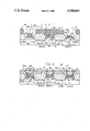
- FIG. 1 shows in side sectional view a partially fabricated CMOS EPROM device of this invention at a stage at which dopants are selectively introduced into the substrate to form the source and drain.
- FIG. 2 shows in side sectional view the CMOS EPROM of FIG. 1 after completion of all diffusions, metallization and passivation.
- a P-type substrate 12 upon which a self-aligned EPROM and both P-channel and N-channel peripheral transistors are to be formed is covered with a silicon dioxide layer that is formed by exposing substrate 12 to a high temperature in the presence of oxygen. After this initial oxidation, a conventional photoresist etch is performed. In this etching step, a layer of photoresist is used to selectively etch the oxide layer creating an aperture in the oxide layer.
- N-well ion implant wherein N-type ions such as phosphorous ions bombard the entire substrate surface. However, only the region of substrate 12 beneath the oxide aperture receives these N-type ions causing a predetermined concentration of impurities in region 18.
- N-well diffusion is performed.
- the substrate is raised to a high temperature, approximately 1200°. This high temperature causes the N-type dopant to migrate forming an N-well 18 in FIG. 1.
- well 18 has a depth of approximately a few thousand angstroms. After the diffusion, it has a depth of approximately 30,000 angstroms. This creates the N-well in which the P-channel transistor is built.
- silicon dioxide layer 14 grows several hundred angstroms because of further oxidation. Silicon nitride is then deposited on the surface of oxide layer 14 forming a nitride layer that is then etched through a photoresist masking layer to mask all the regions where a device is to be built, whether the device is an EPROM device, a P-channel transistor, or an N-channel transistor. This etching removes the regions of the silicon nitride layer not covered by the mask.
- P+ guard rings 26 are formed by a blanket boron implant.
- guard rings 26 After the formation of guard rings 26 the photoresist masking layer is removed and a new photoresist masking layer is provided which is used with the remaining patches of the nitride layer as masks to a phosphosous ion implant to create N+ guard ring 28 with N-well 18.
- That photoresist layer is then removed and a field oxidation is performed during which the substrate is subjected to a high temperature for a long period of time causing oxide layer 14 to become greatly enlarged as shown in FIG. 1.
- the remaining patches of nitride layer 22 are then removed.
- the removal of the nitride layer is followed by a blanket channel implant with a P-conductivity type impurity such as boron.
- a P-conductivity type impurity such as boron.
- the threshold of all three devices are adjusted.
- the regions under the enlarged oxide layer 14 are, of course, not affected by this implant.
- the enlarged regions of oxide layer 14 are too thick for the implant to penetrate and serve as a mask.
- Silicon dioxide region 40 covers the substrate 12 at this point.
- the ultimate thickness of the oxide at the channel regions will also determine the threshold of the EPROM and the N-channel and P-channel devices. However, the thickness of region 40 was not precisely controlled, and is removed.
- a high quality insulating oxide layer 42 is grown in the same location from which oxide layer 40 was removed.
- the oxidation to form layer 42 is followed by deposition of a layer of polysilicon.
- This first polysilicon layer is formed of conventional polycrystalline silicon which is deposited in a conventional vapor depositing step. It may be doped with N+ type ions to make it more conductive. This may be accomplished by a standard phosphorous diffusion step, known as POCl 3 doping to impart conductivity to the polysilicon layer 44 amounting to about 15 ohms per square.
- the first polysilicon layer is removed except at the area of the entire EPROM device, and the areas just over a central part of each of the P-channel and N-channel devices to define the gates 44b and 44c, respectively, of the P-channel and N-channel devices. Those remaining polysilicon regions are then oxidized to form the silicon oxide layer 46.
- a second blanket layer of polycrystalline silicon is deposited upon the substrate and is doped with N-type dopant, thereby creating a highly conductive N+ second polycrystalline layer.
- a photoresist layer covers the peripheral devices gate regions, namely both P-channel transistor region 36 and N-channel transistor region 38, and separately covers a central portion of N+ polysilicon layer above EPROM channel region 32.
- the first etch is an N+ polysilicon etch which removes the second N+ polysilicon layer except for the central portion of the photoresist layer.
- the second etch is a buffered-hydrofluoric polycrystalline-oxide etch which removes polycrystalline oxide layer 46 except for the central portion of the photoresist layer.
- the final etch is a polysilicon etch which removes the first polysilicon layer except for the portion below the central portion of the photoresist layer.
- a new photoresist layer is formed to cover the EPROM region 32, leaving open the polysilicon layer 44b above P-channel region 36 and the polysilicon layer 44c above the N-channel region 38.
- the second polysilicon layer portion overlying the N- and P-channel regions is then removed and a second polysilicon oxidation step is performed which results in the formation of the polysilicon oxide layer 62 on the EPROM gate structure shown in FIG. 1 and also adds thickness to the oxide layer 46 that covers P-channel gate 44b and N-channel gate 44c.
- a p-type ion implant is performed with another masking layer preventing ions from being implanted in the N-channel transistor region 38 and in the EPROM device channel region 32, while P-channel gate 44b, along with its oxide layer 46, prevent p-type ions from entering channel region 36 underneath them.
- the enlarged regions of oxide layer 14 prevent the p-type ions from being implanted in N+ guard rings 28.
- Photoresist layer 68 has aperture 70 above the region where the N-channel transistor is to be formed and aperture 72 above the region where the EPROM device is to be formed. Following the formation of apertures 70 and 72 in layer 68, N-type arsenic ions are implanted. N-channel transistor gate 44c and its oxide layer 46 protect a portion of N-channel region 38 from receiving the ion implants. This results in the formation of N+ source and drain regions 74 and 75 which provides gate-aligned channels 32 and 38.
- control gate 52a and floating gate 44a protect a portion of the N-channel EPROM region 32 thereby causing the ion implant to form N+ source and drain regions 76 and 77.
- the source and drain regions 76 and 77 of the N-channel EPROM device and 74 and 75 of the N-channel transistor are formed simultaneously, and are called self-aligned N+ sources and drains.
- the sources 74 and 76 and drains 75 and 77 of the N-channel transistor device and EPROM device are subjected to a second implant, this time of phosphorous ions which is also an N-type dopant, through the same apertures 70 and 72 of the photoresist mask 68.
- One object of this second doping is to create an EPROM drain of a high density core of arsenic ions for making good ohmic contact thereto and to form around this core a low density N-type shell of phosphorous ions that extend under the EPROM floating gate 44a' to effect an improved EPROM programming efficiency.
- a second object of this second doping is to reduce the drain to body leakage and to reduce the chances of a short between the metal 80 and drain 75 and/or 77 at the silicon surface under the "birds beak" field region between the P+ stops 26 and the only-arsenic doped drains 75 and 77 as seen in FIG. 1.
- Such an undesirable leakage, or short condition may be brought about by a slight misregistration between the metal contacts 80 and the EPROM and N-channel devices.
- the improvement in programming efficiency is accomplished by the phosphorous drain extension under the floating electrode 44a' and it is therefore only necessary to apply the second phosphorous doping to the drains, and not the sources, of the EPROM device. To dope only the drains will require an additional photoresist masking step for covering the sources and opening the drains.
- the secondary doping (with phosphorous) must also be applied to the sources.
- a further advantage of phosphorous doping to both the sources and drains is that no additional photomask is required.
- the phosphorous implant is done using the same mask 68 as was used for the arsenic implant.
- a contact etching step is performed.
- glass is deposited on the surface and heated until it reflows slightly, thereby forming reflow glass layer 78.
- Photoresist is then deposited and contact holes are cut to all source, drain and gate regions. The photoresist is then removed.
- a metal alloy is then deposited. This metal alloy comes in contact with the areas beneath the apertures which have been etched in glass layer 78, thereby forming metal contacts 80. This is followed by a metal photoresist masking and a metal etch which leaves metal above the regions to which the contact is required. A passivation layer 82 is then deposited and etched, resulting in the final structure as shown in FIG. 2.
- Tests of programming efficiency were conducted on experimental EPROM devices of this invention, and on another group of EPROM devices that had no secondary (phosphorous) doping of the source and drain.
- Each device was programmed by connecting substrate and source to ground potential and momentarily connecting the drain and control gate to a +15V potential.
- a 1500 ohm resistor was connected between the drain and the +15V supply.
- the momentary connection of +15V to the control gate and drain was varied over the range of 0.5 to 10 milliseconds. After programming at each "pulse" width, the read threshold voltage at which the control gate must be raised, to make the EPROM channel conductive, was measured.
- the threshold voltages were respectively 3.3 volts, 4.8 volts and 5.9 volts when the programming duration was at 0.5 milliseconds.
- the threshold voltages were, respectively, 6.2 volts (with no phosphorous implant), 6.9 volts and 7.7 volts.
Abstract
Description
Claims (3)
Priority Applications (1)
| Application Number | Priority Date | Filing Date | Title |
|---|---|---|---|
| US06/680,199 US4590665A (en) | 1984-12-10 | 1984-12-10 | Method for double doping sources and drains in an EPROM |
Applications Claiming Priority (1)
| Application Number | Priority Date | Filing Date | Title |
|---|---|---|---|
| US06/680,199 US4590665A (en) | 1984-12-10 | 1984-12-10 | Method for double doping sources and drains in an EPROM |
Publications (1)
| Publication Number | Publication Date |
|---|---|
| US4590665A true US4590665A (en) | 1986-05-27 |
Family
ID=24730136
Family Applications (1)
| Application Number | Title | Priority Date | Filing Date |
|---|---|---|---|
| US06/680,199 Expired - Lifetime US4590665A (en) | 1984-12-10 | 1984-12-10 | Method for double doping sources and drains in an EPROM |
Country Status (1)
| Country | Link |
|---|---|
| US (1) | US4590665A (en) |
Cited By (24)
| Publication number | Priority date | Publication date | Assignee | Title |
|---|---|---|---|---|
| US4649629A (en) * | 1985-07-29 | 1987-03-17 | Thomson Components - Mostek Corp. | Method of late programming a read only memory |
| US4737471A (en) * | 1985-06-19 | 1988-04-12 | Fujitsu Limited | Method for fabricating an insulated-gate FET having a narrow channel width |
| US4774202A (en) * | 1985-11-07 | 1988-09-27 | Sprague Electric Company | Memory device with interconnected polysilicon layers and method for making |
| US4775642A (en) * | 1987-02-02 | 1988-10-04 | Motorola, Inc. | Modified source/drain implants in a double-poly non-volatile memory process |
| US4804637A (en) * | 1985-09-27 | 1989-02-14 | Texas Instruments Incorporated | EEPROM memory cell and driving circuitry |
| US4830974A (en) * | 1988-01-11 | 1989-05-16 | Atmel Corporation | EPROM fabrication process |
| US4939558A (en) * | 1985-09-27 | 1990-07-03 | Texas Instruments Incorporated | EEPROM memory cell and driving circuitry |
| US5051793A (en) * | 1989-03-27 | 1991-09-24 | Ict International Cmos Technology, Inc. | Coplanar flash EPROM cell and method of making same |
| US5145798A (en) * | 1982-08-30 | 1992-09-08 | Texas Instruments Incorporated | Method of fabricating an insulated gate field effect transistor having lightly-doped source and drain extensions using an oxide sidewall spacer method |
| US5149665A (en) * | 1991-07-10 | 1992-09-22 | Micron Technology, Inc. | Conductive source line for high density programmable read-only memory applications |
| US5185279A (en) * | 1987-03-31 | 1993-02-09 | Kabushiki Kaisha Toshiba | Method of manufacturing insulated-gate type field effect transistor |
| US5257095A (en) * | 1985-12-04 | 1993-10-26 | Advanced Micro Devices, Inc. | Common geometry high voltage tolerant long channel and high speed short channel field effect transistors |
| US5270240A (en) * | 1991-07-10 | 1993-12-14 | Micron Semiconductor, Inc. | Four poly EPROM process and structure comprising a conductive source line structure and self-aligned polycrystalline silicon digit lines |
| US5352620A (en) * | 1984-05-23 | 1994-10-04 | Hitachi, Ltd. | Method of making semiconductor device with memory cells and peripheral transistors |
| US5641982A (en) * | 1994-10-31 | 1997-06-24 | Nec Corporation | High voltage mosfet with an improved channel stopper structure |
| US5656527A (en) * | 1990-09-22 | 1997-08-12 | Samsung Electronics Co., Ltd. | Method for fabricating a non-volatile semiconductor memory device having storage cell array and peripheral circuit, and a structure therefore |
| US5687113A (en) * | 1994-03-30 | 1997-11-11 | Sgs-Thomson Microelectronics S.A. | Electrically programmable memory cell |
| US5903494A (en) * | 1994-03-30 | 1999-05-11 | Sgs-Thomson Microelectronics S.A. | Electrically programmable memory cell |
| US5923969A (en) * | 1997-01-07 | 1999-07-13 | Kabushiki Kaisha Toshiba | Method for manufacturing a semiconductor device having a limited pocket region |
| US6174759B1 (en) * | 1998-05-04 | 2001-01-16 | U.S. Philips Corporation | Method of manufacturing a semiconductor device |
| US6350641B1 (en) * | 2000-05-17 | 2002-02-26 | United Microelectronics Corp. | Method of increasing the depth of lightly doping in a high voltage device |
| US6596567B1 (en) * | 1997-09-26 | 2003-07-22 | United Microelectronics Corporation | Method for fabricating a semiconductor device having a impurity layer disposed between a non-doped silicon film and high melting-point metal film for reducing solid state reaction between said high melting-point metal film and polycrystal silicon film |
| US20040137674A1 (en) * | 2002-12-30 | 2004-07-15 | Han Chang Hun | Method of manufacturing an EEPROM device |
| US6878596B2 (en) * | 2002-07-18 | 2005-04-12 | Hynix Semiconductor Inc. | Method of forming high voltage junction in semiconductor device |
Citations (8)
| Publication number | Priority date | Publication date | Assignee | Title |
|---|---|---|---|---|
| US4119995A (en) * | 1976-08-23 | 1978-10-10 | Intel Corporation | Electrically programmable and electrically erasable MOS memory cell |
| US4369072A (en) * | 1981-01-22 | 1983-01-18 | International Business Machines Corp. | Method for forming IGFET devices having improved drain voltage characteristics |
| US4373249A (en) * | 1980-02-20 | 1983-02-15 | Hitachi, Ltd. | Method of manufacturing a semiconductor integrated circuit device |
| US4472871A (en) * | 1978-09-21 | 1984-09-25 | Mostek Corporation | Method of making a plurality of MOSFETs having different threshold voltages |
| US4488351A (en) * | 1983-01-27 | 1984-12-18 | Tokyo Shibaura Denki Kabushiki Kaisha | Method for manufacturing semiconductor device |
| US4495693A (en) * | 1980-06-17 | 1985-01-29 | Tokyo Shibaura Denki Kabushiki Kaisha | Method of integrating MOS devices of double and single gate structure |
| US4514897A (en) * | 1979-09-04 | 1985-05-07 | Texas Instruments Incorporated | Electrically programmable floating gate semiconductor memory device |
| US4517732A (en) * | 1982-10-05 | 1985-05-21 | Fujitsu Limited | Method for fabricating an EEPROM |
-
1984
- 1984-12-10 US US06/680,199 patent/US4590665A/en not_active Expired - Lifetime
Patent Citations (9)
| Publication number | Priority date | Publication date | Assignee | Title |
|---|---|---|---|---|
| US4119995A (en) * | 1976-08-23 | 1978-10-10 | Intel Corporation | Electrically programmable and electrically erasable MOS memory cell |
| US4119995B1 (en) * | 1976-08-23 | 1982-11-02 | ||
| US4472871A (en) * | 1978-09-21 | 1984-09-25 | Mostek Corporation | Method of making a plurality of MOSFETs having different threshold voltages |
| US4514897A (en) * | 1979-09-04 | 1985-05-07 | Texas Instruments Incorporated | Electrically programmable floating gate semiconductor memory device |
| US4373249A (en) * | 1980-02-20 | 1983-02-15 | Hitachi, Ltd. | Method of manufacturing a semiconductor integrated circuit device |
| US4495693A (en) * | 1980-06-17 | 1985-01-29 | Tokyo Shibaura Denki Kabushiki Kaisha | Method of integrating MOS devices of double and single gate structure |
| US4369072A (en) * | 1981-01-22 | 1983-01-18 | International Business Machines Corp. | Method for forming IGFET devices having improved drain voltage characteristics |
| US4517732A (en) * | 1982-10-05 | 1985-05-21 | Fujitsu Limited | Method for fabricating an EEPROM |
| US4488351A (en) * | 1983-01-27 | 1984-12-18 | Tokyo Shibaura Denki Kabushiki Kaisha | Method for manufacturing semiconductor device |
Non-Patent Citations (4)
| Title |
|---|
| Ohta et al., IEEE Trans. Electron Devices ED 27, (1980), 1352. * |
| Ohta et al., IEEE Trans. Electron Devices ED-27, (1980), 1352. |
| S. Fukunaga et al., FA CMOS Process for Low Power PROM with Low Avalanche Injection Voltage, International Electron Devices Meeting (IEEE Conference), 1977. * |
| S. Fukunaga et al., FA-CMOS Process for Low Power PROM with Low Avalanche Injection Voltage, International Electron Devices Meeting (IEEE Conference), 1977. |
Cited By (27)
| Publication number | Priority date | Publication date | Assignee | Title |
|---|---|---|---|---|
| US5145798A (en) * | 1982-08-30 | 1992-09-08 | Texas Instruments Incorporated | Method of fabricating an insulated gate field effect transistor having lightly-doped source and drain extensions using an oxide sidewall spacer method |
| US5352620A (en) * | 1984-05-23 | 1994-10-04 | Hitachi, Ltd. | Method of making semiconductor device with memory cells and peripheral transistors |
| US4737471A (en) * | 1985-06-19 | 1988-04-12 | Fujitsu Limited | Method for fabricating an insulated-gate FET having a narrow channel width |
| US4649629A (en) * | 1985-07-29 | 1987-03-17 | Thomson Components - Mostek Corp. | Method of late programming a read only memory |
| US4804637A (en) * | 1985-09-27 | 1989-02-14 | Texas Instruments Incorporated | EEPROM memory cell and driving circuitry |
| US4939558A (en) * | 1985-09-27 | 1990-07-03 | Texas Instruments Incorporated | EEPROM memory cell and driving circuitry |
| US4774202A (en) * | 1985-11-07 | 1988-09-27 | Sprague Electric Company | Memory device with interconnected polysilicon layers and method for making |
| US5257095A (en) * | 1985-12-04 | 1993-10-26 | Advanced Micro Devices, Inc. | Common geometry high voltage tolerant long channel and high speed short channel field effect transistors |
| US4775642A (en) * | 1987-02-02 | 1988-10-04 | Motorola, Inc. | Modified source/drain implants in a double-poly non-volatile memory process |
| US5185279A (en) * | 1987-03-31 | 1993-02-09 | Kabushiki Kaisha Toshiba | Method of manufacturing insulated-gate type field effect transistor |
| US4830974A (en) * | 1988-01-11 | 1989-05-16 | Atmel Corporation | EPROM fabrication process |
| US5051793A (en) * | 1989-03-27 | 1991-09-24 | Ict International Cmos Technology, Inc. | Coplanar flash EPROM cell and method of making same |
| US5656527A (en) * | 1990-09-22 | 1997-08-12 | Samsung Electronics Co., Ltd. | Method for fabricating a non-volatile semiconductor memory device having storage cell array and peripheral circuit, and a structure therefore |
| US5270240A (en) * | 1991-07-10 | 1993-12-14 | Micron Semiconductor, Inc. | Four poly EPROM process and structure comprising a conductive source line structure and self-aligned polycrystalline silicon digit lines |
| US5149665A (en) * | 1991-07-10 | 1992-09-22 | Micron Technology, Inc. | Conductive source line for high density programmable read-only memory applications |
| US5687113A (en) * | 1994-03-30 | 1997-11-11 | Sgs-Thomson Microelectronics S.A. | Electrically programmable memory cell |
| US5740103A (en) * | 1994-03-30 | 1998-04-14 | Sgs-Thomson Microelectronics S.A. | Electrically programmable memory cell |
| US5903494A (en) * | 1994-03-30 | 1999-05-11 | Sgs-Thomson Microelectronics S.A. | Electrically programmable memory cell |
| US5641982A (en) * | 1994-10-31 | 1997-06-24 | Nec Corporation | High voltage mosfet with an improved channel stopper structure |
| US5923969A (en) * | 1997-01-07 | 1999-07-13 | Kabushiki Kaisha Toshiba | Method for manufacturing a semiconductor device having a limited pocket region |
| US6596567B1 (en) * | 1997-09-26 | 2003-07-22 | United Microelectronics Corporation | Method for fabricating a semiconductor device having a impurity layer disposed between a non-doped silicon film and high melting-point metal film for reducing solid state reaction between said high melting-point metal film and polycrystal silicon film |
| US6800911B2 (en) | 1997-09-26 | 2004-10-05 | United Microelectronics Corporation | Method of making a polycide interconnection layer having a silicide film formed on a polycrystal silicon for a semiconductor device |
| US6174759B1 (en) * | 1998-05-04 | 2001-01-16 | U.S. Philips Corporation | Method of manufacturing a semiconductor device |
| US6350641B1 (en) * | 2000-05-17 | 2002-02-26 | United Microelectronics Corp. | Method of increasing the depth of lightly doping in a high voltage device |
| US6878596B2 (en) * | 2002-07-18 | 2005-04-12 | Hynix Semiconductor Inc. | Method of forming high voltage junction in semiconductor device |
| US20040137674A1 (en) * | 2002-12-30 | 2004-07-15 | Han Chang Hun | Method of manufacturing an EEPROM device |
| US6984590B2 (en) * | 2002-12-30 | 2006-01-10 | Dongbu Anam Semiconductor Inc. | Method of manufacturing an EEPROM device |
Similar Documents
| Publication | Publication Date | Title |
|---|---|---|
| US4590665A (en) | Method for double doping sources and drains in an EPROM | |
| US4598460A (en) | Method of making a CMOS EPROM with independently selectable thresholds | |
| US4646425A (en) | Method for making a self-aligned CMOS EPROM wherein the EPROM floating gate and CMOS gates are made from one polysilicon layer | |
| US6514830B1 (en) | Method of manufacturing high voltage transistor with modified field implant mask | |
| US4968639A (en) | Process for manufacturing CMOS integrated devices with reduced gate lengths | |
| US5977591A (en) | High-voltage-resistant MOS transistor, and corresponding manufacturing process | |
| US6127696A (en) | High voltage MOS transistor for flash EEPROM applications having a uni-sided lightly doped drain | |
| US4422885A (en) | Polysilicon-doped-first CMOS process | |
| US5216272A (en) | High withstanding voltage MIS transistor | |
| US4135955A (en) | Process for fabricating high voltage cmos with self-aligned guard rings utilizing selective diffusion and local oxidation | |
| US5834352A (en) | Methods of forming integrated circuits containing high and low voltage field effect transistors therein | |
| US6159795A (en) | Low voltage junction and high voltage junction optimization for flash memory | |
| US4235011A (en) | Semiconductor apparatus | |
| JP2001313374A (en) | Method for manufacturing integrated circuit integrating electrically programmable nonvolatile memory and high performance logic circuit net in identical semiconductor chip | |
| US4745083A (en) | Method of making a fast IGFET | |
| US6274914B1 (en) | CMOS integrated circuits including source/drain plug | |
| EP0545082B1 (en) | Process for manufacturing MOS-type integrated circuits comprising LOCOS isolation regions | |
| KR100318283B1 (en) | Planar process using common registration mark for well injection | |
| US4488348A (en) | Method for making a self-aligned vertically stacked gate MOS device | |
| KR100427959B1 (en) | Method of manufacturing a pic(power integrated circuit) device, and a pic device manufactured by such a method | |
| US6069033A (en) | Method of manufacturing a non-volatile memory and a CMOS transistor | |
| JPS59204232A (en) | Method of forming ion implanted region | |
| US4223334A (en) | High voltage CMOS with local oxidation for self-aligned guard rings and process of fabrication | |
| WO1998044552A9 (en) | Method of manufacturing a non-volatile memory combining an eprom with a standard cmos process | |
| US5486487A (en) | Method for adjusting the threshold of a read-only memory to achieve low capacitance and high breakdown voltage |
Legal Events
| Date | Code | Title | Description |
|---|---|---|---|
| AS | Assignment |
Owner name: SOLID STATE SCIENTIFIC, INC., WILLOW GROVE, PENNSY Free format text: ASSIGNMENT OF ASSIGNORS INTEREST.;ASSIGNORS:OWENS, ALEXANDER H.;HALFACRE, MARK A.;HUIE, WING K.;AND OTHERS;REEL/FRAME:004519/0544 Effective date: 19850114 Owner name: SOLID STATE SCIENTIFIC, INC., A CORP OF DELAWARE,P Free format text: ASSIGNMENT OF ASSIGNORS INTEREST;ASSIGNORS:OWENS, ALEXANDER H.;HALFACRE, MARK A.;HUIE, WING K.;AND OTHERS;REEL/FRAME:004519/0544 Effective date: 19850114 |
|
| STCF | Information on status: patent grant |
Free format text: PATENTED CASE |
|
| AS | Assignment |
Owner name: SPRAGUE ELECTRIC COMPANY, A MASSACHUSETTS CORP. Free format text: ASSIGNMENT OF ASSIGNORS INTEREST.;ASSIGNOR:SOLID STATE SCIENTIFIC, INC.,;REEL/FRAME:004819/0744 Effective date: 19870806 |
|
| FEPP | Fee payment procedure |
Free format text: PAYOR NUMBER ASSIGNED (ORIGINAL EVENT CODE: ASPN); ENTITY STATUS OF PATENT OWNER: LARGE ENTITY |
|
| FPAY | Fee payment |
Year of fee payment: 4 |
|
| AS | Assignment |
Owner name: ALLEGRO MICROSYSTEMS, INC., A CORP. OF DE Free format text: ASSIGNMENT OF ASSIGNORS INTEREST.;ASSIGNOR:SPRAGUE ELECTRIC COMPANY, A CORP. OF MA;REEL/FRAME:005610/0139 Effective date: 19910131 |
|
| FPAY | Fee payment |
Year of fee payment: 8 |
|
| FPAY | Fee payment |
Year of fee payment: 12 |