US4592075A - Phase-shift keying demodulator - Google Patents
Phase-shift keying demodulator Download PDFInfo
- Publication number
- US4592075A US4592075A US06/694,202 US69420285A US4592075A US 4592075 A US4592075 A US 4592075A US 69420285 A US69420285 A US 69420285A US 4592075 A US4592075 A US 4592075A
- Authority
- US
- United States
- Prior art keywords
- signal
- phase
- product
- psk
- computing
- Prior art date
- Legal status (The legal status is an assumption and is not a legal conclusion. Google has not performed a legal analysis and makes no representation as to the accuracy of the status listed.)
- Expired - Fee Related
Links
- 230000010363 phase shift Effects 0.000 title description 3
- 239000000969 carrier Substances 0.000 claims abstract description 16
- 238000001514 detection method Methods 0.000 description 5
- 230000000630 rising effect Effects 0.000 description 4
- 230000003111 delayed effect Effects 0.000 description 3
- 238000010586 diagram Methods 0.000 description 3
- 238000010276 construction Methods 0.000 description 2
- 238000000034 method Methods 0.000 description 1
- 238000012986 modification Methods 0.000 description 1
- 230000004048 modification Effects 0.000 description 1
- 238000010791 quenching Methods 0.000 description 1
- 230000000171 quenching effect Effects 0.000 description 1
- 238000005070 sampling Methods 0.000 description 1
- 238000007493 shaping process Methods 0.000 description 1
- 230000006641 stabilisation Effects 0.000 description 1
- 238000011105 stabilization Methods 0.000 description 1
Images


Classifications
-
- H—ELECTRICITY
- H04—ELECTRIC COMMUNICATION TECHNIQUE
- H04L—TRANSMISSION OF DIGITAL INFORMATION, e.g. TELEGRAPHIC COMMUNICATION
- H04L27/00—Modulated-carrier systems
- H04L27/18—Phase-modulated carrier systems, i.e. using phase-shift keying
- H04L27/22—Demodulator circuits; Receiver circuits
- H04L27/227—Demodulator circuits; Receiver circuits using coherent demodulation
- H04L27/2271—Demodulator circuits; Receiver circuits using coherent demodulation wherein the carrier recovery circuit uses only the demodulated signals
- H04L27/2273—Demodulator circuits; Receiver circuits using coherent demodulation wherein the carrier recovery circuit uses only the demodulated signals associated with quadrature demodulation, e.g. Costas loop
-
- H—ELECTRICITY
- H04—ELECTRIC COMMUNICATION TECHNIQUE
- H04L—TRANSMISSION OF DIGITAL INFORMATION, e.g. TELEGRAPHIC COMMUNICATION
- H04L27/00—Modulated-carrier systems
- H04L27/0014—Carrier regulation
- H04L2027/0044—Control loops for carrier regulation
- H04L2027/0046—Open loops
- H04L2027/0048—Frequency multiplication
-
- H—ELECTRICITY
- H04—ELECTRIC COMMUNICATION TECHNIQUE
- H04L—TRANSMISSION OF DIGITAL INFORMATION, e.g. TELEGRAPHIC COMMUNICATION
- H04L27/00—Modulated-carrier systems
- H04L27/0014—Carrier regulation
- H04L2027/0044—Control loops for carrier regulation
- H04L2027/0063—Elements of loops
- H04L2027/0067—Phase error detectors
-
- H—ELECTRICITY
- H04—ELECTRIC COMMUNICATION TECHNIQUE
- H04L—TRANSMISSION OF DIGITAL INFORMATION, e.g. TELEGRAPHIC COMMUNICATION
- H04L27/00—Modulated-carrier systems
- H04L27/0014—Carrier regulation
- H04L2027/0044—Control loops for carrier regulation
- H04L2027/0071—Control of loops
- H04L2027/0073—Detection of synchronisation state
Definitions
- the present invention relates to a phase-shift keying (PSK) demodulator, and more particularly to a phase-shift keying demodulator for restoring digital data by reproducing a carrier and a clock signal from a signal modulated by PSK.
- PSK phase-shift keying
- a PSK demodulator having two phase detectors for detecting the phase of a PSK signal and a carrier generator for supplying carriers of different phases to the two phase detectors, respectively, the PSK demodulator also including squaring means for squaring output signals from the two phase detectors, difference computing means for computing the difference between output signals from the squaring means, product computing means for computing the product of the output signals from the two phase detectors, and product detecting means for detecting the product of an output signal from the product computing means and an output signal from the difference computing means, the arrangement being such that the frequencies and phases of the carriers generated by the carrier generator are controlled by an output signal from the product detecting means.
- FIGS. 1, 2A and 2B are illustrative of operation of a PSK demodulator
- FIG. 3 is a block diagram of a conventional PSK demodulator
- FIG. 4 is a timing chart showing operation of the conventional PSK demodulator of FIG. 3;
- FIG. 5 is a block diagram of a PSK demodulator according to the present invention.
- FIG. 6 is a diagram showing operation of the PSK demodulator of the present invention.
- FIG. 7 is a timing chart showing operation of the PSK demodulator of the present invention.
- FIGS. 3 and 5 Designated in FIGS. 3 and 5 at 1 a quadruple multiplier, 2 a bandpass filter, 3, 14, 14', 24, 24' waveform shapers, 4 a divide-by-4 frequency divider, 5, 6, 26 one-shot multivibrators, 7, 27 phase comparators, 8, 28 switches, 9, 13, 13', 23, 29 low-pass filters, 10, 30 amplifiers, 11, 31 voltage-controlled oscillators, 12, 12', 18, 18', 20, 21 multipliers, 15, 15' D-type flip-flops, 16 a phase shifter, 19 a differential amplifier, and 25 an AND circuit.
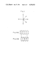
- arrows (1) through (4) indicate phases of a four-phase PSK signal at respective four values thereof which are angularly equally spaced by 90 degrees.
- the signals at the respective phases can generally be expressed by sin ⁇ t, cos ⁇ t, -sin ⁇ t, and -cos ⁇ t, respectively.
- FIG. 2A shows the waveform of an output signal generated by detecting a four-phase PSK signal, the waveform being called an eye pattern. Since digital data is required to be sampled at maximum amplitudes of the eye pattern, a clock signal for sampling the data has to have rising or falling edges at the maximum amplitudes of the eye pattern as illustrated in FIG. 2B.
- a carrier reproducing system employed in a conventional four-phase PSK demodulator shown in FIG. 3 is a so-called quadruple system in which a carrier a is reproduced from a four-phase PSK signal A by the components designated at 1 through 4. More specifically, the frequency of the four-phase PSK siganl A is quadrupled by the quadruple multiplier 1 to elimiate phase information. The multiplied signal is then passed through a bandpass filter 2 which picks up a signal of a fourfold frequency that is applied to the waveform shaper 3. A shaped signal issued from the waveform shaper 3 is then applied to the divide-by-4 frequency divider 4 which produces the desired carrier a with its frequency divided by four.
- a clock signal used for bit synchronization in the conventional device shown in FIG. 3 is reproduced from a detected output signal d by the components denoted at 5 through 11. More specifically, the one-shot multivibrator 5 produces a pulse signal e (indicated at e in FIG. 4) having a prescribed width Ti with rising and falling edges of the detected output signal d, and the pulse signal e is applied to the other one-shot multivibrator 6 and the phase comparator 7.
- the one-shot multivibrator 6 is retriggerable to generate a pulse singal f (indicated at f in FIG. 4) of a width such as equal to a one-bit data width To shown in FIG.
- the switch 8 comprises an analog switch, for example, and supplies a signal from the phase comparator 7 to the low-pass filter 9 only when the pulse signal f is in the ON state.
- a signal from the low-pass filter 9 is amplified by the amplifier 10, and the amplified signal is then applied to the voltage-controlled oscillator 11 which issues a clock signal g (indicated at g in FIG. 4) of ceratin time intervals to the phase comparator 7.
- the above arrangement constitutes a PLL (phase-locked loop) to produce the clock signal g in synchronism with the signal d.
- the prior construction is however disadvantageous in that when a preset pulse width in the one-shot multivibrator is varied, no pulse signal of a duty cycle of 50% can be produced, and a simple and stable circuit such as an exclosive-OR phase comparator cannot be employed as the phase comparator 7. Furthermore, the optimum timing of the clock signal corresponds to the falling edges of the pulse signal e, as shown in FIG. 4, making unstable the characteristics of the feedback loop because of the phase characteristics of the exclusive-OR phase comparator. Solving this shortcoming requires a 90°-phase shifter connected to an output terminal of the voltage-controlled oscillator 11 or another phase comparator having a wide detecting range.
- the four-phase PSK signal is demodulated by applying the four-phase PSK signal A and the carrier a reproduced by the quadruple system, as shown in FIG. 3, to the multiplier 12, applying an output signal from the multiplier 12 to the low-pass filter 13 to extract a signal component c corresponding to the phase difference, and thereafter shaping the waveform of the signal c with the waveform shaper 14 to produce the detected output signal d.
- the clock signal g reproduced by the components 5 through 11 is supplied to the D-type flip-flop 15 to extract prescribed digital data B from the detected output signal d.
- the delayed carrier signal b is applied to the multiplier 12', rom which digital data C is obtained through the low-pass filter 13', the waveform shaper 14', and the D-type flipflop 15'.
- a PSK signal is detected with carriers having difference phases, and the detected signals are squared to erase their polarity, followed by negative feedback control of the frequencies and phases of the carriers based on the difference between the signals for stable detection.
- a four-phase PSK siganl A and a carrier a issued from the voltage controlled oscillator 17 which constitutes a PLL, described later, are applied to the multiplier 12, an output signal of which is fed to the low-pass filter 13 to extract a signal c (indicated at c in FIG. 7) having a frequency corresponding to the phase difference between the signals A and a.
- the signal c is then applied to the waveform shaper 14 which issues a detected output signal d, from which digital data B is extracted by a clock signal g, described later, supplied to the D-type flip-flop 15.
- digital data C is extracted through the multiplier 12', the low-pass filter 13', the waveform shaper 14', and the D-type flip-flop 15' from the four-phase PSK signal A and a carrier which is 90 degrees delayed in phase from the carrier a issued from the voltage-controlled oscillator 17.
- the carrier a issued from the voltage-controlled oscillator 17 and the four-phase PSK signal A are applied to the multiplier 12, and the signal detected by the multiplier 12 is squared by the multiplier 18 to erase the polarity of the signal, thus producing a signal with its polarity erased, that is, an output h (indicated at h in FIG. 7) in the form of sin 2 ⁇ or cos 2 ⁇ .
- the four-phase signal A and the carrier which is 90 degrees delayed in phase from the carrier a from the voltage-controlled oscillator 17 are applied to the multiplier 12', an output signal from which is fed to the multiplier 18' to produce a signal h' (indicated at h' in FIG. 7) with its poraliry erased.
- the signals h and h' (sin 2 ⁇ or cos 2 ⁇ ) thus produced are applied to the differential amplifier 19 which produces a differential signal (sin 2 ⁇ -cos 2 ⁇ ) or (cos 2 ⁇ -sin 2 ⁇ ).
- the differential signal and a polarity signal p issued from the multiplier 21 are applied to the multiplier 20.
- the four-phase PSK signal is expressed in the form having the phases (1) through (4) as shown in FIG. 1.
- sin ⁇ cos ⁇
- the differential output signal (sin 2 ⁇ -cos 2 ⁇ ) or (cos 2 ⁇ -sin 2 ⁇ ) from the differential amplifier 19 should be zero so as to constitute a PLL.
- the signals c, c' can be produced by detecting PSK signals corresponding to the phases (1) through (4) in the column of the input signals shown in FIG. 6 with the multiplifiers 12, 12'.
- the signals obtained by multiplying the signals c, c' with the multiplier 12 have signs as indicated in the column p of FIG. 6.
- the signals produced by squaring the signals c, c' are as shown in the columns h, h'. Therefore, by multiplying, with the multiplier 20, the output signal (sin 2 ⁇ -cos 2 ⁇ ) or (cos 2 ⁇ -sin 2 ⁇ ) from the differential amplifier 19 of FIG. 5 by signal p having the sign indicated in the column p of FIG.
- a signal can be obtained at all times in the form of (sin 2 ⁇ -cos 2 ⁇ ).
- the carrier b can be produced by delaying the phase of the carrier a by 90 degrees.
- the signals h, h' (indicated at h, h' in FIG. 7) squared by the multiplifers 18, 18' shown in FIG. 5 are applied to the waveform shapers 24, 24', respectively, which generate shaped signals i, i' (indicated at i. i' in FIG. 7), respectively.
- the signals i, i' are then fed to the AND circuit 25 which issues an signal j (indicated at j in FIG. 7) indicative of a logical product.
- a PLL circuit is driven for increased stability and reliability.
- the signal j is supplied to the one-shot multivibrator 26 and the phase comparator 27.
- the one-shot multivibrator 26 is retriggerable to produce a signal k (indicated at k in FIG. 7) having a pulse width corresponding to the one-bit data width To with rising edges of the signal j indicated by the arrows in FIG. 7.
- the switch 28 comprising an analog switch, for example, is driven by the signal k.
- the switch 28 serves to increase the gain of the PLL.
- phase comparator 27 An output from the phase comparator 27 is supplied through the switch 28, the low-pass filter 29, and the amplifier 30 to the voltage-controlled oscillator 31, an arrangement which constitutes the PLL for stably and reliably reproducing the clock signal g (indicated at g in FIG. 7) in synchronism with the signals h, h'. Since the synchronizing signal is extracted after the detected signal has been squared, any unstability encountered in forming the pulse signal of a duty cycle of 50% with the conventional one-shot multivibrator 5 shown in FIG. 3 is eliminated, and a phase comparator such for example as an exclusive-OR phase comparator of a simple construction can be employed.
- a PSK signal is detected with carriers of different phases, the detected signals are squared to erase their polarity, and thereafter the frequencies and phases of the carriers are controlled by negative feedback based on the difference between the detected signals. Therefore, the frequencies of the carriers reproduced will not be shifted which would otherwise be shafted by a certain data pattern as in the quadruple system, and the reproduced carriers can reliably be brought into synchronism.
- the reproduced carriers can reliably be brought into synchronism particularly because their frequencies and phases are controlled by feeding phase error signals contained in the output signals from the phase detectors (multipliers 12, 12') directly to the carrier oscillator (voltage-controlled oscillator 17) through a negative feedback loop. Since the PLL includes no digital circuit, it requires no waveform shaper and is simple in circuit arrangemetnt for easier stabilization of the reproduced carrier.
Abstract
A PSK demodulator has two phase detectors for detecting the phase of a PSK signal and a carrier generator for supplying carriers of different phases to the two phase detectors, respectively. The PSK demodulator also includes squaring means for squaring output signals from the two phase detectors, difference computing means for computing the difference between output signals from the squaring means, product computing means for computing the product of the output signals from the two phase detectors, and product detecting means for detecting the product of an output signal from the product computing means and an output signal from the difference computing means, the arrangement being such that the frequencies and phases of the carriers generated by the carrier generator are controlled by an output signal from the product detecting means.
Description
The present invention relates to a phase-shift keying (PSK) demodulator, and more particularly to a phase-shift keying demodulator for restoring digital data by reproducing a carrier and a clock signal from a signal modulated by PSK.
For demodulating a PSK signal, it is necessary to reproduce a carrier and a clock signal which are suppressed in principle.
There has heretofore been employed a quadruple system in which a received four-phase PSK signal is multiplied by four and then frequency-divided by four to erase phase information for thereby reproducing a desired carrier. The quadruple system is however liable to be affected by a data pattern contained in the received singal. Where data are received which are successive in the order of sinωt, -cos ωt, -sin ωt and cos ωt, the frequency of the reproduced carrier tends to be shifted so that no stable carrier can be obtained.
When reproducing a clock signal from the detected signal for bit synchronization, it is difficult to generate stably a pulse signal having a duty cycle of 50% with respect to a data bit width, and therefore it is difficult to produce a stable clock signal with a phase comparator composed of a simple exclusive-OR logic circuit.
It is an object of the present invention to eliminate the above conventional problems by detecting a PSK signal with two carriers having different phases, squaring the detected signals to erase their polarity, and thereafter controlling the frequencies and phases of the carriers by negative feedback based on the difference between the signals for stable signal detection.
According to the present invention, there is provided a PSK demodulator having two phase detectors for detecting the phase of a PSK signal and a carrier generator for supplying carriers of different phases to the two phase detectors, respectively, the PSK demodulator also including squaring means for squaring output signals from the two phase detectors, difference computing means for computing the difference between output signals from the squaring means, product computing means for computing the product of the output signals from the two phase detectors, and product detecting means for detecting the product of an output signal from the product computing means and an output signal from the difference computing means, the arrangement being such that the frequencies and phases of the carriers generated by the carrier generator are controlled by an output signal from the product detecting means.
The above and other objects, features and advantages of the present invention will become more apparent from the following description when taken in conjunction with the accompanying drawings in which a preferred embodiment of the present invention is shown by way of illustrative example.
FIGS. 1, 2A and 2B are illustrative of operation of a PSK demodulator;
FIG. 3 is a block diagram of a conventional PSK demodulator;
FIG. 4 is a timing chart showing operation of the conventional PSK demodulator of FIG. 3;
FIG. 5 is a block diagram of a PSK demodulator according to the present invention;
FIG. 6 is a diagram showing operation of the PSK demodulator of the present invention; and
FIG. 7 is a timing chart showing operation of the PSK demodulator of the present invention.
Like or corresponding parts are denoted by like or corresponding reference characters throughout several views.
Designated in FIGS. 3 and 5 at 1 a quadruple multiplier, 2 a bandpass filter, 3, 14, 14', 24, 24' waveform shapers, 4 a divide-by-4 frequency divider, 5, 6, 26 one-shot multivibrators, 7, 27 phase comparators, 8, 28 switches, 9, 13, 13', 23, 29 low-pass filters, 10, 30 amplifiers, 11, 31 voltage-controlled oscillators, 12, 12', 18, 18', 20, 21 multipliers, 15, 15' D-type flip-flops, 16 a phase shifter, 19 a differential amplifier, and 25 an AND circuit.
As shown in FIG. 1, arrows (1) through (4) indicate phases of a four-phase PSK signal at respective four values thereof which are angularly equally spaced by 90 degrees. The signals at the respective phases can generally be expressed by sin ωt, cos ωt, -sin ωt, and -cos ωt, respectively.
Arrows (5) and (6) are indicative of phases of reproducing carriers required for phase detection. Where 74 is 45 degrees, sin θ=cos θ, which is a condition preferred for detection as described below.
FIG. 2A shows the waveform of an output signal generated by detecting a four-phase PSK signal, the waveform being called an eye pattern. Since digital data is required to be sampled at maximum amplitudes of the eye pattern, a clock signal for sampling the data has to have rising or falling edges at the maximum amplitudes of the eye pattern as illustrated in FIG. 2B.
A carrier reproducing system employed in a conventional four-phase PSK demodulator shown in FIG. 3 is a so-called quadruple system in which a carrier a is reproduced from a four-phase PSK signal A by the components designated at 1 through 4. More specifically, the frequency of the four-phase PSK siganl A is quadrupled by the quadruple multiplier 1 to elimiate phase information. The multiplied signal is then passed through a bandpass filter 2 which picks up a signal of a fourfold frequency that is applied to the waveform shaper 3. A shaped signal issued from the waveform shaper 3 is then applied to the divide-by-4 frequency divider 4 which produces the desired carrier a with its frequency divided by four. In the quadruple system, however, the freuqency of the reproduced carrier a sometimes tends to be shifted where a particular data patter such as of sin ωt, -cos ωt, -sin ωt and cos ωt is received. Although this problem can be eliminated by so-called quenching to initialize the bandpass filter 2 when the data pattern is varied, such a solution makes it difficult to match timing.
A clock signal used for bit synchronization in the conventional device shown in FIG. 3 is reproduced from a detected output signal d by the components denoted at 5 through 11. More specifically, the one-shot multivibrator 5 produces a pulse signal e (indicated at e in FIG. 4) having a prescribed width Ti with rising and falling edges of the detected output signal d, and the pulse signal e is applied to the other one-shot multivibrator 6 and the phase comparator 7. The one-shot multivibrator 6 is retriggerable to generate a pulse singal f (indicated at f in FIG. 4) of a width such as equal to a one-bit data width To shown in FIG. 4 each time a rising edge of the pulse signal e is detected, and applies the pulse signal f to the switch 8. The switch 8 comprises an analog switch, for example, and supplies a signal from the phase comparator 7 to the low-pass filter 9 only when the pulse signal f is in the ON state. A signal from the low-pass filter 9 is amplified by the amplifier 10, and the amplified signal is then applied to the voltage-controlled oscillator 11 which issues a clock signal g (indicated at g in FIG. 4) of ceratin time intervals to the phase comparator 7. The above arrangement constitutes a PLL (phase-locked loop) to produce the clock signal g in synchronism with the signal d. The prior construction is however disadvantageous in that when a preset pulse width in the one-shot multivibrator is varied, no pulse signal of a duty cycle of 50% can be produced, and a simple and stable circuit such as an exclosive-OR phase comparator cannot be employed as the phase comparator 7. Furthermore, the optimum timing of the clock signal corresponds to the falling edges of the pulse signal e, as shown in FIG. 4, making unstable the characteristics of the feedback loop because of the phase characteristics of the exclusive-OR phase comparator. Solving this shortcoming requires a 90°-phase shifter connected to an output terminal of the voltage-controlled oscillator 11 or another phase comparator having a wide detecting range.
As is known in the art, the four-phase PSK signal is demodulated by applying the four-phase PSK signal A and the carrier a reproduced by the quadruple system, as shown in FIG. 3, to the multiplier 12, applying an output signal from the multiplier 12 to the low-pass filter 13 to extract a signal component c corresponding to the phase difference, and thereafter shaping the waveform of the signal c with the waveform shaper 14 to produce the detected output signal d. The clock signal g reproduced by the components 5 through 11 is supplied to the D-type flip-flop 15 to extract prescribed digital data B from the detected output signal d. In addition, after delaying the phase of the carrier a by 90 degrees with the phase shifter 16, the delayed carrier signal b is applied to the multiplier 12', rom which digital data C is obtained through the low-pass filter 13', the waveform shaper 14', and the D-type flipflop 15'.
According to the present invention, a PSK signal is detected with carriers having difference phases, and the detected signals are squared to erase their polarity, followed by negative feedback control of the frequencies and phases of the carriers based on the difference between the signals for stable detection.
A process for demodulating a four-phase PSK signal in the device of the invention will be described with reference to FIG. 5.
For generating a detected output signal d, a four-phase PSK siganl A and a carrier a issued from the voltage controlled oscillator 17 which constitutes a PLL, described later, are applied to the multiplier 12, an output signal of which is fed to the low-pass filter 13 to extract a signal c (indicated at c in FIG. 7) having a frequency corresponding to the phase difference between the signals A and a. The signal c is then applied to the waveform shaper 14 which issues a detected output signal d, from which digital data B is extracted by a clock signal g, described later, supplied to the D-type flip-flop 15.
Likewise, digital data C is extracted through the multiplier 12', the low-pass filter 13', the waveform shaper 14', and the D-type flip-flop 15' from the four-phase PSK signal A and a carrier which is 90 degrees delayed in phase from the carrier a issued from the voltage-controlled oscillator 17.
An arrangement and operation for reproducing the carrier a from the four-phase PSK signal A will be described with reference to FIG. 5.
The carrier a issued from the voltage-controlled oscillator 17 and the four-phase PSK signal A are applied to the multiplier 12, and the signal detected by the multiplier 12 is squared by the multiplier 18 to erase the polarity of the signal, thus producing a signal with its polarity erased, that is, an output h (indicated at h in FIG. 7) in the form of sin2 θ or cos2 θ.
Similarly, the four-phase signal A and the carrier which is 90 degrees delayed in phase from the carrier a from the voltage-controlled oscillator 17 are applied to the multiplier 12', an output signal from which is fed to the multiplier 18' to produce a signal h' (indicated at h' in FIG. 7) with its poraliry erased.
The signals h and h' (sin2 θ or cos2 θ) thus produced are applied to the differential amplifier 19 which produces a differential signal (sin2 θ-cos2 θ) or (cos2 θ-sin2 θ). The differential signal and a polarity signal p issued from the multiplier 21 are applied to the multiplier 20.
As described above, the four-phase PSK signal is expressed in the form having the phases (1) through (4) as shown in FIG. 1. Where the phase of the carrier a supplied to the multipliers 12, 12' for phase detection is selected to be θ=45 degrees at (5) and (6) in FIG. 1, sin θ=cos θ, and the differential output signal (sin2 θ-cos2 θ) or (cos2 θ-sin2 θ) from the differential amplifier 19 should be zero so as to constitute a PLL.
The signals c, c' can be produced by detecting PSK signals corresponding to the phases (1) through (4) in the column of the input signals shown in FIG. 6 with the multiplifiers 12, 12'. The signals obtained by multiplying the signals c, c' with the multiplier 12 have signs as indicated in the column p of FIG. 6. The signals produced by squaring the signals c, c' are as shown in the columns h, h'. Therefore, by multiplying, with the multiplier 20, the output signal (sin2 θ-cos2 θ) or (cos2 θ-sin2 θ) from the differential amplifier 19 of FIG. 5 by signal p having the sign indicated in the column p of FIG. 6, a signal can be obtained at all times in the form of (sin2 θ-cos2 θ). By feeding the signal from the multiplier 20 to the voltage-controlled oscillator 17 through the low-pass filter 23 via a negative feedback loop, there is obtained the carrier a having a desired frequency and phase shown at (5) in FIG. 1 with θ=45 degrees. The carrier b can be produced by delaying the phase of the carrier a by 90 degrees.
The reproduction of a clock signal for bit synchronization will be described in detail with reference to FIGS. 5 and 7.
The signals h, h' (indicated at h, h' in FIG. 7) squared by the multiplifers 18, 18' shown in FIG. 5 are applied to the waveform shapers 24, 24', respectively, which generate shaped signals i, i' (indicated at i. i' in FIG. 7), respectively. The signals i, i' are then fed to the AND circuit 25 which issues an signal j (indicated at j in FIG. 7) indicative of a logical product. Although it is posible to sample digital data B, C from the signals d, d' using the signal j, a PLL circuit is driven for increased stability and reliability. To this end, the signal j is supplied to the one-shot multivibrator 26 and the phase comparator 27. The one-shot multivibrator 26 is retriggerable to produce a signal k (indicated at k in FIG. 7) having a pulse width corresponding to the one-bit data width To with rising edges of the signal j indicated by the arrows in FIG. 7. The switch 28 comprising an analog switch, for example, is driven by the signal k. The switch 28 serves to increase the gain of the PLL. An output from the phase comparator 27 is supplied through the switch 28, the low-pass filter 29, and the amplifier 30 to the voltage-controlled oscillator 31, an arrangement which constitutes the PLL for stably and reliably reproducing the clock signal g (indicated at g in FIG. 7) in synchronism with the signals h, h'. Since the synchronizing signal is extracted after the detected signal has been squared, any unstability encountered in forming the pulse signal of a duty cycle of 50% with the conventional one-shot multivibrator 5 shown in FIG. 3 is eliminated, and a phase comparator such for example as an exclusive-OR phase comparator of a simple construction can be employed.
With the arrangement of the present invention, as described above, a PSK signal is detected with carriers of different phases, the detected signals are squared to erase their polarity, and thereafter the frequencies and phases of the carriers are controlled by negative feedback based on the difference between the detected signals. Therefore, the frequencies of the carriers reproduced will not be shifted which would otherwise be shafted by a certain data pattern as in the quadruple system, and the reproduced carriers can reliably be brought into synchronism. The reproduced carriers can reliably be brought into synchronism particularly because their frequencies and phases are controlled by feeding phase error signals contained in the output signals from the phase detectors (multipliers 12, 12') directly to the carrier oscillator (voltage-controlled oscillator 17) through a negative feedback loop. Since the PLL includes no digital circuit, it requires no waveform shaper and is simple in circuit arrangemetnt for easier stabilization of the reproduced carrier.
Although a certain preferred embodiment has been shown and described, it should be understood that many changes and modifications may be made therein without departing from the scope of the appended claims.
Claims (3)
1. A PSK demodulator having two phase detectors for detecting the phase of a PSK signal and a carrier generator for supplying carriers of different phases to the two phase detectors, respectively, said PSK demodulator comprising squaring means for squaring output signals from said two phase detectors, difference computing means for computing the difference between output signals from the squaring means, product computing means for computing the product of the output signals from said two phase detectors, and product detecting means for detecting the product of an output signal from said product computing means and an output signal from said difference computing means, the arrangement being such that the frequencies and phases of the carriers generated by said carrier generator are controlled by an output signal from said product detecting means.
2. A PSK demodulator according to claim 1, wherein said squaring means comprises a pair of multipliers for squaring the output signals, respectively, from said two phase detectors.
3. A PSK demodulator according to claim 2, wherein said difference computing means comprises a differential amplifier for determining the difference between output signals from said multipliers.
Applications Claiming Priority (2)
| Application Number | Priority Date | Filing Date | Title |
|---|---|---|---|
| JP59-11389 | 1984-01-25 | ||
| JP59011389A JPS60154758A (en) | 1984-01-25 | 1984-01-25 | Psk demodulator |
Publications (1)
| Publication Number | Publication Date |
|---|---|
| US4592075A true US4592075A (en) | 1986-05-27 |
Family
ID=11776650
Family Applications (1)
| Application Number | Title | Priority Date | Filing Date |
|---|---|---|---|
| US06/694,202 Expired - Fee Related US4592075A (en) | 1984-01-25 | 1985-01-24 | Phase-shift keying demodulator |
Country Status (2)
| Country | Link |
|---|---|
| US (1) | US4592075A (en) |
| JP (1) | JPS60154758A (en) |
Cited By (8)
| Publication number | Priority date | Publication date | Assignee | Title |
|---|---|---|---|---|
| US4843616A (en) * | 1987-03-10 | 1989-06-27 | Ant Nachrichtentechnik Gmbh | Method of obtaining a phase difference signal |
| US4847869A (en) * | 1987-12-04 | 1989-07-11 | Motorla, Inc. | Rapid reference acquisition and phase error compensation for radio transmission of data |
| US4894845A (en) * | 1987-06-02 | 1990-01-16 | U.S. Philips Corporation | Receiver for a phase-shift keyed carrier signal |
| US5307021A (en) * | 1991-09-19 | 1994-04-26 | Nec Corporation | Phase-error detecting circuit for QDPSK demodulator |
| US5311545A (en) * | 1991-06-17 | 1994-05-10 | Hughes Aircraft Company | Modem for fading digital channels affected by multipath |
| US5579345A (en) * | 1994-10-13 | 1996-11-26 | Westinghouse Electric Corporation | Carrier tracking loop for QPSK demodulator |
| US20050111582A1 (en) * | 2003-10-17 | 2005-05-26 | Sony Corporation | Digital modulation circuit and method as well as digital demodulation circuit and method |
| US9729365B2 (en) * | 2014-03-06 | 2017-08-08 | Robert Bosch Gmbh | DARC signal demodulation circuit arrangement and method for operating same |
Citations (16)
| Publication number | Priority date | Publication date | Assignee | Title |
|---|---|---|---|---|
| US3204185A (en) * | 1961-04-19 | 1965-08-31 | North American Aviation Inc | Phase-lock receivers |
| US3594651A (en) * | 1969-10-15 | 1971-07-20 | Communications Satellite Corp | Quadriphase modem |
| US3990016A (en) * | 1975-04-23 | 1976-11-02 | Donald Dimon | Asynchronous demodulator |
| US4092606A (en) * | 1977-06-21 | 1978-05-30 | Lovelace Alan M Acting Adminis | Quadraphase demodulation |
| US4137505A (en) * | 1975-04-16 | 1979-01-30 | Patelhold Patentverwertungs- & Holding Ag | Method of and apparatus for frequency control |
| US4143322A (en) * | 1976-09-30 | 1979-03-06 | Nippon Electric Co., Ltd. | Carrier wave recovery system apparatus using synchronous detection |
| US4188589A (en) * | 1978-09-01 | 1980-02-12 | Motorola, Inc. | Automatic signal acquisition means for a phase locked loop with anti-sideband lock protection |
| US4238739A (en) * | 1979-02-26 | 1980-12-09 | E-Systems, Inc. | Preset network for a phase lock loop |
| US4255713A (en) * | 1978-03-03 | 1981-03-10 | Nippon Electric Co., Ltd. | Carrier regeneration circuit for polyphase modulation system |
| JPS56140746A (en) * | 1980-04-02 | 1981-11-04 | Nippon Telegr & Teleph Corp <Ntt> | Carrier wave reproducing circuit for multi-value qam |
| US4318049A (en) * | 1978-02-17 | 1982-03-02 | The Marconi Company Limited | Carrier recovery circuit for use in a multi-level phase shift keying demodulator |
| US4336500A (en) * | 1980-07-14 | 1982-06-22 | Motorola, Inc. | MSK Demodulator frequency acquistion apparatus and method |
| US4359692A (en) * | 1980-11-07 | 1982-11-16 | Motorola Inc. | Rapid acquisition shift keyed signal demodulator |
| US4408351A (en) * | 1979-01-26 | 1983-10-04 | Licentia Patent-Verwaltungs-Gmbh | Directly mixing receiving system |
| US4470145A (en) * | 1982-07-26 | 1984-09-04 | Hughes Aircraft Company | Single sideband quadricorrelator |
| US4517680A (en) * | 1983-02-23 | 1985-05-14 | Paradyne Corporation | Error vector normalizer |
Family Cites Families (1)
| Publication number | Priority date | Publication date | Assignee | Title |
|---|---|---|---|---|
| JPS52119853A (en) * | 1976-04-01 | 1977-10-07 | Toshiba Corp | Automatic phase control circuit |
-
1984
- 1984-01-25 JP JP59011389A patent/JPS60154758A/en active Pending
-
1985
- 1985-01-24 US US06/694,202 patent/US4592075A/en not_active Expired - Fee Related
Patent Citations (16)
| Publication number | Priority date | Publication date | Assignee | Title |
|---|---|---|---|---|
| US3204185A (en) * | 1961-04-19 | 1965-08-31 | North American Aviation Inc | Phase-lock receivers |
| US3594651A (en) * | 1969-10-15 | 1971-07-20 | Communications Satellite Corp | Quadriphase modem |
| US4137505A (en) * | 1975-04-16 | 1979-01-30 | Patelhold Patentverwertungs- & Holding Ag | Method of and apparatus for frequency control |
| US3990016A (en) * | 1975-04-23 | 1976-11-02 | Donald Dimon | Asynchronous demodulator |
| US4143322A (en) * | 1976-09-30 | 1979-03-06 | Nippon Electric Co., Ltd. | Carrier wave recovery system apparatus using synchronous detection |
| US4092606A (en) * | 1977-06-21 | 1978-05-30 | Lovelace Alan M Acting Adminis | Quadraphase demodulation |
| US4318049A (en) * | 1978-02-17 | 1982-03-02 | The Marconi Company Limited | Carrier recovery circuit for use in a multi-level phase shift keying demodulator |
| US4255713A (en) * | 1978-03-03 | 1981-03-10 | Nippon Electric Co., Ltd. | Carrier regeneration circuit for polyphase modulation system |
| US4188589A (en) * | 1978-09-01 | 1980-02-12 | Motorola, Inc. | Automatic signal acquisition means for a phase locked loop with anti-sideband lock protection |
| US4408351A (en) * | 1979-01-26 | 1983-10-04 | Licentia Patent-Verwaltungs-Gmbh | Directly mixing receiving system |
| US4238739A (en) * | 1979-02-26 | 1980-12-09 | E-Systems, Inc. | Preset network for a phase lock loop |
| JPS56140746A (en) * | 1980-04-02 | 1981-11-04 | Nippon Telegr & Teleph Corp <Ntt> | Carrier wave reproducing circuit for multi-value qam |
| US4336500A (en) * | 1980-07-14 | 1982-06-22 | Motorola, Inc. | MSK Demodulator frequency acquistion apparatus and method |
| US4359692A (en) * | 1980-11-07 | 1982-11-16 | Motorola Inc. | Rapid acquisition shift keyed signal demodulator |
| US4470145A (en) * | 1982-07-26 | 1984-09-04 | Hughes Aircraft Company | Single sideband quadricorrelator |
| US4517680A (en) * | 1983-02-23 | 1985-05-14 | Paradyne Corporation | Error vector normalizer |
Cited By (9)
| Publication number | Priority date | Publication date | Assignee | Title |
|---|---|---|---|---|
| US4843616A (en) * | 1987-03-10 | 1989-06-27 | Ant Nachrichtentechnik Gmbh | Method of obtaining a phase difference signal |
| US4894845A (en) * | 1987-06-02 | 1990-01-16 | U.S. Philips Corporation | Receiver for a phase-shift keyed carrier signal |
| US4847869A (en) * | 1987-12-04 | 1989-07-11 | Motorla, Inc. | Rapid reference acquisition and phase error compensation for radio transmission of data |
| US5311545A (en) * | 1991-06-17 | 1994-05-10 | Hughes Aircraft Company | Modem for fading digital channels affected by multipath |
| US5307021A (en) * | 1991-09-19 | 1994-04-26 | Nec Corporation | Phase-error detecting circuit for QDPSK demodulator |
| US5579345A (en) * | 1994-10-13 | 1996-11-26 | Westinghouse Electric Corporation | Carrier tracking loop for QPSK demodulator |
| US20050111582A1 (en) * | 2003-10-17 | 2005-05-26 | Sony Corporation | Digital modulation circuit and method as well as digital demodulation circuit and method |
| US7903760B2 (en) * | 2003-10-17 | 2011-03-08 | Sony Corporation | Digital modulation circuit and method as well as digital demodulation circuit and method |
| US9729365B2 (en) * | 2014-03-06 | 2017-08-08 | Robert Bosch Gmbh | DARC signal demodulation circuit arrangement and method for operating same |
Also Published As
| Publication number | Publication date |
|---|---|
| JPS60154758A (en) | 1985-08-14 |
Similar Documents
| Publication | Publication Date | Title |
|---|---|---|
| US4015083A (en) | Timing recovery circuit for digital data | |
| JPS599668U (en) | carrier synchronizer | |
| US4592075A (en) | Phase-shift keying demodulator | |
| US4345211A (en) | Digital phaselock demodulator | |
| US3970945A (en) | Method and apparatus for demodulating PSK modulated oscillations | |
| JPS6347182B2 (en) | ||
| JPS5835428B2 (en) | Carrier wave regeneration circuit | |
| US4656431A (en) | Digital frequency discriminator | |
| EP0259867A2 (en) | Demodulator for psk-modulated signals | |
| US4882546A (en) | Demodulation clock generator circuit | |
| US4618830A (en) | PSK demodulator using asynchronous local oscillator | |
| US4686689A (en) | Phase-locked loop circuit | |
| EP0204464B1 (en) | Clock synchronizing circuit including a voltage controlled oscillator | |
| GB1507638A (en) | Receiver for synchronous data signals | |
| JPS6225543A (en) | Frequency stabilizing system for local oscillator | |
| JPS6330023A (en) | Circuit with phase locking loop | |
| JPS60113557A (en) | Carrier wave reproducing circuit | |
| JPH08154090A (en) | Synchronizing signal generator | |
| US4847578A (en) | Method and device for detecting false locks between a reference signal and a signal to be demodulated by coherent digital demodulation | |
| JP2553643B2 (en) | Carrier synchronizer | |
| JP2600668B2 (en) | Clock regeneration circuit | |
| JPS61142842A (en) | Carrier wave lead-in auxiliary system | |
| KR100339392B1 (en) | Apparatus for recovering clock of digital demodulating system | |
| JP2756965B2 (en) | Demodulator for high transmission rate modulated signal | |
| JPS60154757A (en) | Psk demodulator |
Legal Events
| Date | Code | Title | Description |
|---|---|---|---|
| AS | Assignment |
Owner name: ALPS ELECTRIC CO.,LTD 1-7 YUKIGAYA OTSUKA-CHO, OT Free format text: ASSIGNMENT OF ASSIGNORS INTEREST.;ASSIGNOR:TSUKAMOTO, AKIHITO;REEL/FRAME:004362/0852 Effective date: 19840905 |
|
| REMI | Maintenance fee reminder mailed | ||
| LAPS | Lapse for failure to pay maintenance fees | ||
| STCH | Information on status: patent discontinuation |
Free format text: PATENT EXPIRED DUE TO NONPAYMENT OF MAINTENANCE FEES UNDER 37 CFR 1.362 |
|
| FP | Lapsed due to failure to pay maintenance fee |
Effective date: 19900527 |