US4638190A - Digitally controlled wideband phase shifter - Google Patents
Digitally controlled wideband phase shifter Download PDFInfo
- Publication number
- US4638190A US4638190A US06/735,990 US73599085A US4638190A US 4638190 A US4638190 A US 4638190A US 73599085 A US73599085 A US 73599085A US 4638190 A US4638190 A US 4638190A
- Authority
- US
- United States
- Prior art keywords
- mesfet
- signal
- set forth
- segment
- segments
- Prior art date
- Legal status (The legal status is an assumption and is not a legal conclusion. Google has not performed a legal analysis and makes no representation as to the accuracy of the status listed.)
- Expired - Fee Related
Links
Images


Classifications
-
- H—ELECTRICITY
- H03—ELECTRONIC CIRCUITRY
- H03H—IMPEDANCE NETWORKS, e.g. RESONANT CIRCUITS; RESONATORS
- H03H11/00—Networks using active elements
- H03H11/02—Multiple-port networks
- H03H11/16—Networks for phase shifting
- H03H11/20—Two-port phase shifters providing an adjustable phase shift
-
- H—ELECTRICITY
- H01—ELECTRIC ELEMENTS
- H01Q—ANTENNAS, i.e. RADIO AERIALS
- H01Q3/00—Arrangements for changing or varying the orientation or the shape of the directional pattern of the waves radiated from an antenna or antenna system
- H01Q3/26—Arrangements for changing or varying the orientation or the shape of the directional pattern of the waves radiated from an antenna or antenna system varying the relative phase or relative amplitude of energisation between two or more active radiating elements; varying the distribution of energy across a radiating aperture
- H01Q3/30—Arrangements for changing or varying the orientation or the shape of the directional pattern of the waves radiated from an antenna or antenna system varying the relative phase or relative amplitude of energisation between two or more active radiating elements; varying the distribution of energy across a radiating aperture varying the relative phase between the radiating elements of an array
- H01Q3/34—Arrangements for changing or varying the orientation or the shape of the directional pattern of the waves radiated from an antenna or antenna system varying the relative phase or relative amplitude of energisation between two or more active radiating elements; varying the distribution of energy across a radiating aperture varying the relative phase between the radiating elements of an array by electrical means
- H01Q3/36—Arrangements for changing or varying the orientation or the shape of the directional pattern of the waves radiated from an antenna or antenna system varying the relative phase or relative amplitude of energisation between two or more active radiating elements; varying the distribution of energy across a radiating aperture varying the relative phase between the radiating elements of an array by electrical means with variable phase-shifters
- H01Q3/38—Arrangements for changing or varying the orientation or the shape of the directional pattern of the waves radiated from an antenna or antenna system varying the relative phase or relative amplitude of energisation between two or more active radiating elements; varying the distribution of energy across a radiating aperture varying the relative phase between the radiating elements of an array by electrical means with variable phase-shifters the phase-shifters being digital
- H01Q3/385—Scan control logics
Definitions
- the invention relates to phase shifting means, and more particularly to digitally stepped phase shifting means suitable for operation at frequencies ranging from a fraction of a gigahertz to many gigahertz. Phase shifting finds major application to antenna arrays.
- MMIC Monolithic microwave integrated circuit
- phase shifting is required in the reception or transmission of signals involving antenna arrays, wherein the phase must be adjusted either row by row or element by element.
- the phase control is used to alter the mode of the array or to steer the beam.
- the phase adjusting means depending on the number of rows or elements of the array, must be of such accuracy as to preserve the accuracy inherent in the array itself. In such applications digital control is particularly desirable.
- the phase adjusting means should be sufficiently broadband as not to distort the signal, often broadband, being processed.
- phase shifter comprises phase splitting means for resolving an input signal to be phase shifted into a first and a second vector component in mutual quadrature, a first and a second dual gate MESFET, each having source, drain, signal gate and n-fold control gate terminals, each MESFET being subdivided into an n-fold plurality of segments.
- Each MESFET segment has a predetermined width to achieve a desired transconductance, and various combinations of segments are selectively activated by a control signal, to provide successive transfer values (i.e. scaling factors) respectively proportional to the sine and cosine of successive angle thetas, resulting from stepping the phase shifter.
- means are provided for combining the quadrature related, sine and cosine proportioned vector components at the output of the two MESFETS to form an output signal which represents the desired stepped rotation of the input signal by the angle theta.
- each MESFET segment has an electroded source region connected to a common MESFET source terminal, an electroded drain region connected to a common MESFET drain terminal, and a gate region defined between source and drain regions having a signal gate electrode for modifying the AC output signal current of the MESFET as a function of the segment transconductance, and an activating gate electrode disposed between the signal gate electrode and the drain for turning current flow "ON" or "OFF" in the MESFET segment.
- the same design may be used for generating either sine or cosine values.
- a six bit control signal and two three segment MESFETS are adequate, with the segment widths being in the proportions of 1:3.613:7.524.
- the phase shifter particularly at higher frequencies is preferably fabricated using MMIC (monolithic microwave integrated circuit) techniques on a monocrystalline substrate.
- MMIC monolithic microwave integrated circuit
- semiconducting regions are formed on the substrate.
- the segments of the MESFETS are formed in the semiconducting regions, and are defined by a photolithographic technique.
- the source, drain, signal gate, and activating gate electrodes of the segments are formed on the monocrystalline substrate, and are defined by a photolithographic technique.
- the connections between the source, drain and gate electrodes of each segment of each MESFET and the source, output, input, and control gate terminals of each MESFET are formed on the monocrystalline substrate and are defined by a photolithographic technique.
- the technique permits the segmented dual gate MESFETS and the passive components required for signal coupling and filtering to be formed on the substrate in a very compact, electrically efficient arrangement which minimizes the reactance of segment interconnections, reduces deleterious parasitics and facilitates broadband MESFET operation, leading to broadband phase shifter operation, limited primarily to the bandwidth of the associated phase splitter.
- the phase splitter may take either the form of a pair of complementary RC networks or a 1/4 wave directional coupler carried out as a twin transmission line.
- FIG. 1 is a simplified, four element block diagram of a novel digitally controlled phase shifter for use from VHF to EHF frequencies;
- FIGS. 2A and 2B are respectively a simplified electrical circuit diagram and a plan view of a single segment of a segmented dual gate MESFET, explanatory of MESFET operation in scaling individual vector components;
- FIGS. 3A, and 3B illustrate two varieties of "phase splitters” suitable for use over portions of the frequency spectrum
- FIG. 4 is an electrical circuit representation of a monolithically integrated circuit for use in a phase shifter for signals from VHF to EHF frequencies and incorporating a pair of segmented dual gate MESFETS to which a pair of quadrature related vector components may be applied to obtain a vector resultant digitally rotated in response to a control signal;
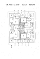
- FIGS. 5A and 5B are respectively plan views of the monolithically integrated circuit illustrated in FIG. 4; FIG. 5A being a view of the complete monolithically integrated circuit and FIG. 5B being a more detailed plan view of a smaller portion of the monolithically integrated circuit confined primarily to a single segmented dual gate MESFET and portions of the passive components coupled to that MESFET, and
- FIGS. 6A and 6B illustrate two arrangements for producing a full 360° of digitally stepped phase rotation.
- the digitally controlled wideband phase shifter which is the subject of the present invention, has the general configuration shown in the block diagram of FIG. 1.
- the phase shifter may be seen to consist of four elements--a phase splitter (11) to which the input signal to be phase shifted is applied, and which resolves the signal into two components, a first and a second segmented dual gate MESFET (12 and 13), represented in the diagram as amplifiers, to the signal inputs of which the signal components are applied and to the control inputs of which, control signals(expressive of a trigonometric function of an angle theta) are applied, and a combining network (14) in which the two amplifier outputs are combined toform an output signal which is a reconstruction of the input signal, phase shifted by the angle theta.
- the phase shifter of FIG. 1 may be formed in one or two integrated assemblies.
- the elements 12, 13, and 14 may be monolithically integrated on a single substrate as indicated by the dotted rectangular outline surrounding theseelements and the use of square connection pads to denote the pads for external connection.
- the radio frequency signal to be phase shifted is applied to the RF input terminal 15 of the phase shifter for application to the phase splitter 11.
- the phase splitter 11 may take several forms of which two examples are provided in FIGS. 3A and 3B.
- the phase splitter splits the input signal into two orthogonally related component vectors (I and Q).
- the relationship between components is often expressed as being "in quadrature", the letter "I” denoting the in phase component at zero or reference phase and the letter “Q" denoting the component in quadrature phase, 90° from zero or reference phase.
- the I and Q components obtained from the phase splitter 11 are coupled respectively to a first and second dual gate MESFET 12 and 13 for scaling in accordance with cosine and sine values respectively of an angle theta equal to the stepped angle of rotation.
- the MESFET 12 is designed to provide a signal transfer function, which in response to a control signal applied in bit parallel, is proportional to the cosine function of the angle theta.
- the MESFET 13 is designed to provide an AC signal transfer function which in response to the control signal applied in bit parallel is proportional to the sine function of the same angle theta characterized above.
- the MESFETS 12 and 13 are active devices which may be adjusted to exhibit stepped attenuation, stepped gain, or stepped attenuation transitioning to gain.
- the "transfer function" of the two MESFETS is one of the above, and is normalized to a common value representing unity. Since the operation of the segmented MESFETS is best represented as amplifiers having stepped transconductances, the input quantities to these devices are characterized as (AC) voltages and the output quantities characterized as (AC) currents. Accordingly, the output of the MESFET 12 is an AC current vector at reference phase equal to the multiplication of the I vector at reference phase by a scaler quantity equal to the cosine of the angle theta. Similarly the output of the MESFET13 is a vector at quadrature phase equal to the multiplication of the Q vector at quadrature phase by a scaler quantity equal to the sine of the angle theta.
- the outputs of the two MESFETS 12 and 13 are then combined in the combiningnetwork 14 to form a vector resultant representing the vector resultant of the input signal rotated by the angle theta, plus a constant insertion phase.
- the vector resultant of the output signal is formed in the combining network 14 and appears at the output terminal P16.
- the MESFET output quantities are AC currents, and their addition straight-forward since they are of the same frequency.
- the common load should be of relatively low impedance (i.e. 50 ohm), so that a direct interconnection of the drains of the MESFETS 12 and 13 will perform the current addition function.
- FIGS. 4, 5A and 5B A more detailed illustration of the digitally controlled phase shifter is provided in FIGS. 4, 5A and 5B.
- the arrangement illustrated in these figures is designed to provide a stepwise count of relative transconductance values to implement sines and cosines of an angle theta required to scale the individual vector components and produce a stepped rotation of the resultant vector at 111/4° intervals between 0° and 90°.
- the sine and cosine are implemented by devices of identical design to insure identical unity vectors in the two branches.
- the scaling values are selected from a restricted set common to the sine and cosine functions but are selected ina sine or cosine sequence by programming the control signal. More particularly, the sine for the angle theta is equal to the cosine of 90° minus theta. If theta takes values which are multiples of 1/4 or of 1/8 of 90°, both the cosine and the sine will be taken from the same restricted set of values. Accordingly, a five segment MESFET is appropriate for 111/2° intervals in the event that an approximationof less than 8/10 of a percent is adequate.
- the segments are selectively activated and theirselective activation may be under a five bit control signal applied to eachof the five segments.
- the precise dimensions of the segments may be calculated assuming that segment transconductance is proportional to the segment width. For 111/4° intervals the segment proportions are
- a three segmentMESFET is appropriate if an error of less than half a percent is acceptable.
- These proportions are 1:3.613:7.524 and the devices may be controlled by a three bit signal.
- the five bit design entailssegments which are respectively 10, 16, 23, 59 and 122 microns.
- FIGS. 2A and 2B An electrical circuit and a layout of a single segment of a segmented dual gate MESFET are shown in FIGS. 2A and 2B respectively.
- the circuit components all bear reference numerals consistent with the assumption thatthe segment depicted in FIGS. 2A and 2B is the first segment of one of the five segment MESFETS shown in FIGS. 4 and 5A and is in fact the MESFET shown in FIG. 5B.
- FIG. 2A a single segment of a segmented MESFET is shown at T16.
- the drawing is legended to indicate that the dimension of the segment is 10 microns. This implies that the width of gate region is 10 microns and that the widths of the other electrodes are all substantially equal and consistent with this width selection for purposes of achieving apredetermined transconductance value.
- the MESFET segment T16 may be seen in FIG. 2A to consist of a source and a drain represented respectively as a first and a second horizontal line connecting two vertical lines.
- the source is represented by the lowermost horizontal line connected to the vertical line extending downward to a ground connection.
- the drain is represented by the uppermost horizontal line connected to the upward extending vertical line.
- the gate region is represented by the vertical line extending between the horizontal lines.
- the drain of T16 (and all other segments of MESFETS 12 and 13) is connected via capacitor C13 to the signal output pad P16 and (in common with all other segments of MESFET 12) via resistor R15, which is bypassed to ground by capacitor C15, to the pad P2 for connection to a source of drain potentials VDD.
- the segment T16 is provided with a first gate represented by an arrow impinging on the vertical line representing the gate region in closest proximity to the source.
- the first gate is the signal gate and it is coupled via capacitor C1 to the signal input gate pad P15.
- a second gate for activating the segment is represented by an arrow impinging on the vertical line representing the gate region between the signal gate and the drain. It is shown coupled via a filter R5, C3 to the segment activating gate pad P4.
- the above described MESFET segment is designed to transform the AC input signal voltage appearing at the number one signal gate via the transconductance of that MESFET segment to an output AC signal current flowing through the drain and load resistance R15.
- the presence of an activating potential on the number two gate allows the transformation of the input signal voltage to an output signal current by allowing the segment to enter the linear active region with higher transconductance saturation current.
- the voltage applied to the activating gate is such as to cause cutoff of the MESFET segment, then no transconductance is evident and no output signal current flows in the drain or load resistance.
- the MESFET segment is operated between signal cutoff where saturation current is substantially extinguished and the highlinear current region (where small increments of voltage on the activating gate electrode produce relatively insubstantial changes in transconductance).
- the MESFET segment illustrated in circuit form in FIG. 2A is also illustrated in plan view in FIG. 2B.
- the external circuit components have been omitted and only the immediate metallizations connected to the MESFET electrodes are shown.
- the source electrode is shown as a rectangular metallization S16 to the left in the drawing in contact with the ground plane.
- the drain electrode is a rectangular metallization D16 to the right in the drawing and of similar shape to the source.
- An air bridge connected at the lower part of D16 and extending to the right where it connects to other drain electrodes of MESFET 12, and which leads via several other intermediate metallizations to C13 and the signal output pad P16.
- the number one signal gate is shown as a verticallyextending line-like metallization G1,16 disposed between source and drain but in closer proximity to the source. It is shown connected to a metallization 30 arranged below it and extending to the right where it interconnects the signal gates of all five segments of MESFET 12, and extends downwards for connection to the pad P15 which supplies the I component input signal to the MESFET 12.
- the number 2 gate or activating gate (G2,16) is the second vertically extending line-like metallization disposed between source and drain, but in closer proximity to the drain.
- the activating gate is shown leading to an upward extending conductor 31 insulated from the ground plane and leading toward the capacitor C3.
- the active regions of all four electrodes (source, number 1 gate, number 2 gate, and drain) of T16 are co-extensive with the width of the gate region and in the T16 example are equal to 10 microns. Assuming that the transconductance is proportional tothe gate width, the T16 segment, when activated, provides an increase in transconductance and output current in proportion to this 10 microns gate width. The other segments, of MESFET 12, all larger, will produce greater increments in transconductance and in output signal current.
- the phase splitter forming the initial block in the phase shifter may take one of several forms.
- the two varieties illustrated in FIGS. 3A and 3B aresuitable for use over portions of the UHF-EHF frequency spectrum in which the segmented gate is an efficient scaler.
- the scaling function provided by the MESFET is a broadband property, extending to quite low frequencies and upward to frequencies where differential path lengths and parasitic inductances and capacitances disturb phase coherencebeyond the system tolerance.
- the phase splitter on the other hand, is normally limited to narrower portions of the frequency spectrum usually small portions of an octave.
- the phase splitter illustrated in FIG. 3A is a network which has a single input for the AC signal and which produces two signal outputs.
- One output which is denominated the "I” output channel, provides an output signal at zero or reference phase.
- the other output, the "Q” output channel provides a signal in quadrature to the "I” output signal.
- the phase relation of the "I” signal to the input signal is not fixed, but at the center of the band is typically 45°.
- the "I” branch of the circuit consists of a capacitor in the series path between the input and output terminals and a resistance connected in shunt between the output terminal and ground.
- the "Q” branch of circuit consists of a resistance inthe series path between the input and output terminals and a capacitor connected in shunt between the output terminal and ground.
- the FIG. 3A circuit is designed for use over a given band of frequencies and is optimum at the design center of the band.
- the circuit produces the ideal orthogonal relationship when the magnitude of the capacitive reactances (which are both equal to each other) are equal to the resistances (which are both equal to each other).
- the bandwidth of this arrangement assuming a tolerance of 5°, is approximately 20% of the bandwidth.
- the resistances and capacitances required to provide the phase shift are relatively small at the higher frequencies and are suited to integration on a substrate common to the segmented dual gate MESFETS, to form a complete phase shifter.
- the chip area required for the capacitors are comparable to the chip area required for the MESFETS illustrated in FIG. 5A.
- FIG. 3B At the upper end of the frequency spectrum (at gigahertz frequencies) the arrangement illustrated in FIG. 3B is also appropriate and may also be monolithically integrated with the MESFET scalers at frequencies above 5 gigaherz.
- the design of FIG. 3B may be called a "3 db quadrature directional coupler", which is a four terminal device consisting of a two coupled transmission lines of quarter wave length.
- the signal input is coupled to the lower left terminal of the lower conductor, and the "I" component is derived from the right terminal of the lower conductor.
- the quadrature phase component appears at the upper left terminal of the upperconductor with the right end being connected to a matched resistive load.
- the circuit of FIG. 3B is of narrower bandwidth than the scaler, and also of narrower bandwidth than the FIG. 3A arrangement.
- the FIG. 3B arrangement performs best at the exact frequency at which the coupled transmission lines exhibit an exact length of quarter wave length.
- the useful band of operation of the FIG. 3Bembodiment is ordinarily 10 to 15% of the center frequency, although more elaborate directional couplers can extend the bandwidth to 50% and higher.
- FIGS. 4, 5A and 5B An integrated circuit suitable for VHF to EHF operation and designed to be combined with one of the splitters illustrated in FIGS. 3A and 3B in performing a stepped one quadrant, phase shift is illustrated in FIGS. 4, 5A and 5B.
- the integrated circuit consists of an input circuit (C1, C2, C14, R1-R4) designed to accept the "I” and "Q” vector components from the phase splitter 11, and two five segment scalers 12, 13 and a combining network 14.
- the combining network 14 consists of a common connection of the drainsof MESFETS 12, 13 to equal load (R15, R16 leading to a common output via capacitor C13 to pad P16)).
- the loads R15, R16 are connected between the drains of 12, 13 and a common source of drain potentials (VDD). The drainsare thus connected together at one terminal of the common coupling capacitor C13, which leads to the RF output pad P16, at which the phase shifted output appears.
- each segment of the I channel dual gate MESFET 12 is similar except for width to the segment T16 already discussed in connection with FIGS. 2A and 2B and they are paralleled to contribute to the total signal output current.
- the sources of the segments T16-T20 are connected together and returned to the substrate ground.
- the number 1 signal gates of the devices T16-T20 are connected together and provided with an I signal from the pad P15 via the input network.
- the input network of the I channel consists of a shunt resistance R1 connected between P15 and ground, a series capacitor C1 and a biasing network (partially shared with the MESFET 13) consisting of the resistance R3 connected between the number 1 gates and the pad P3 to which the signal gate bias -Vgg is applied.
- the pad P13 is bypassed to ground by the capacitor C14.
- the activating gates of the segments T16-T20 are separately bypassed to ground by the respective capacitors C3 to C7 and serially connected via the respective resistances R5 to R9 to the respective pads P4 thru P8 for application of individual activating potentials.
- the drains of the segments T16-T20 are connected together and via load resistance R15 (as earlier noted) to the pad P2 for application of VDD potentials.
- the pad P2 is bypassed by capacitor C15 to ground.
- the drain of the I channel MESFET 12 is further connected to one terminal of the capacitor C1 for coupling to the signal output pad P16 forderivation of the signal output.
- the Q channel is similar to the I channel and consists of a dual gate MESFET consisting of the segments T21-T25. As before, the sources of the segments T21-T25 are connected together and returned to the substrate ground. The number 1 signal gates of the devices T21-T25 are connected together and provided with a Q signal from pad P14 via the input network.
- the input network of the Q channel consists of a shunt resistance R2 connected between pad P14 and ground, a series capacitor C2, and a biasingnetwork (partially shared with the MESFET 12) consisting of the resistance R4 connected between the number 1 gates and the pad P3.
- the activating gates of the segments T21-T25 are separately bypassed to ground via the respectivecapacitors C8 to C12, and serially connected via the respective resistancesR10-R14 to the respective pads P9-P13 for application of individual activating potentials.
- the drains of the segments T21-T25 are connected together and via a load resistance R16 to the pad P1 for application of VDD potentials.
- the pad P1 is bypassed by capacitor C16 to ground.
- the drain of the Q channel MESFET is further connected to one terminal of the capacitor C1 for coupling to the signal output pad P16.
- the MESFETS 12 and 13 are of similar design having segment widths of 10, 16, 23, 59 and 122 microns respectively for scaling individual vector components to achieve consecutive 111/4° steps ina single quadrant of angular rotation of the resultant vector.
- the layouts provided in FIGS. 5A and 5B illustrate respectively the full integrated circuit of which the MESFETS 12 and 13 are parts, and a smaller portion ofthe integrated circuit illustrating primarily the MESFET 12 in the I channel.
- the layout of the individual segments of one dual gate MESFET can best be understood from a consideration of FIG. 5B which deals primarily with MESFET 12.
- the segments T16-T20 of MESFET 12 are arranged with the lowest numbered segment to the left and the highest numbered segment to the right.
- the gate length is measured along the horizontal dimension of the drawing and the gate width is measured along the vertical dimension of the drawing. While the gate lengths of all segments are alike, the gate widths are scaled by the numbers noted above.
- the source is to the left and the drain is to the right.
- the signal gates for all the MESFETS T16-T20 is the line-like electrode (of two line-like electrodes) to the left and all signal gates are connected to the metallization 30 arranged below them which supplies the Icomponent input signal.
- the activating gates are individually supplied from downwardly extending metallizations (31; 32; 33; 34; and 35-36 (shared)) associated with the respective capacitors C3, C4, C5, C6 and C7. These activating metallizations lead via the resistances R5-R9 (which are shown in FIG. 5B)to which the pads P4-P8 (shown only in FIG. 5A) on the left side of the integrated circuit.
- the source connections to ground are directly made forthe segments T16, T17, and T18, the source of T18 however forming the pointof contact for an air bridge connector 37 grounding the lower part of the source of T19 and of both sections of source T20.
- the second air bridge connector 38 supplements conductor 37 grounding the upper parts of the source of T19 and of both sections of source T20.
- the drains of all the devices T16-T20 are connected via an air bridge connector 39 which is supplemented by a further air bridge 40, both of which connect the respective drains of MESFET 12 to a consolidated drain metallization 41.
- the consolidated drain metallization connects the drains of both MESFETS 12 and 13 via capacitor C13 to the RF output pad P16.
- phase shifting arrangement suitable for producing a full 360° ofdigitally stepped phase rotation is illustrated in FIG. 6A.
- the arrangement is depicted in simplified block diagram form, it being understood that the phase splitters switches and the scalers may have differing practical designs depending upon application.
- the phase shifter consists of a first (0°, 180°) splitter 50.
- the phase splitter 50 may take the form of a pair of MESFETS having the signal applied to the gate of the first device,with the gate of the other device being grounded.
- the sources of the two devices are connected together to a common load providing signal coupling from the first to the second device.
- the drains of the two devices are connected to a common source of drain potentials via two separate but equal load resistances.
- the complementary 0°, 180° phases appear at the first and second drains respectively.
- the 0° output from the phase splitter 50 is connected to a (0°, 90°) phase splitter 51 having two outputs, one at zero or reference phase and the other in quadrature (90°) to the reference phase.
- the 180° output from phase splitter 50 is fed to asecond 0°, 90° phase splitter 52, similar to phase splitter 52. At the zero output the phase splitter 52 produces an output of 180° and in the 90° output, the phase splitter 52 produces an output of 270°.
- the four outputs of the phase splitters 51 and 52 are selectively connectedby means of the switches S1 to S4 to the I and Q inputs of a pair of scalers such as are shown in FIGS. 4, 5A and 5B.
- the switches S1 to S4 are preferably MESFET switches subject to electronic control similar to that used to activate the individual segments. Either the zero phase output of the phase splitter 51 is connected via the switch S2 to the Q input of theintegrated circuit 53, or the 180° output of the phase splitter 52 is connected via the switch S3 to the I input of the integrated circuit 53. Similarly, either the 90° output of the phase splitter 51 is connected via the switch S2 to the Q input of the integrated circuit 53 orthe 270° output of the phase splitter 52 is connected via the switchS4 to the Q input of the integrated circuit 53.
- switches S1 and S2 are closed (S3 and S4 are open) and the 0°, 90° outputs from 51 are coupled respectively to the I and Q input pads of the integrated circuits 53. This is consistent with the assumption that in the first quadrant both the sine and the cosine are positive.
- the switch S2 remains closed (S4being open) and S1 is now opened while S3 is closed to invert the sign of the cosine component.
- both switches S1 and S2 are open and both switches S3 and S4 are closed.
- the switch S1 is closed (S3 is open) and S4 isclosed (S2 is open).
- FIG. 6B A second phase shifting arrangement suitable for producing a full 360° of digitally stepped phase rotation is illustrated in FIG. 6B.
- the arrangement is similar to that illustrated in FIG. 6A in that it is a five element four switch arrangement and differs in that 0°, 90° phase splitters are interchanged with 0°, 180° phase splitters and vice versa.
- the combination illustrated in FIG. 6B consists of an initial 0°, 90° phase splitter 60 whose two outputs are connected respectively to a first 0°, 180° phase splitter 61 and to a second 0°, 180° phase splitter 62.
- the four outputs of the two last recited phase splitters define components at each of the four quadrant boundries and a series of switchesS1 to S4 operating in the same manner as described with respect to FIG. 6A change the phase of the signal applied to the I and Q input pads of the integrated circuit 63 to effect full 360° phase rotation.
- the phase shifter herein described makes use of the extraordinary characteristics of a method of circuit fabrication currentlyknown as "MMIC” (monolithic microwave integrated circuit) technology.
- MMIC monolithic microwave integrated circuit
- the term “MMIC” implies a circuit fabrication technique in which active and passive components are formed by a photolithographic process on an insulating substrate having both electrically active regions, in which transistors may be formed, and electrically passive regions, in which conductive runs, transmission lines, inductors, capacitors and resistors may be formed.
- the fabrication technique except for external connections to the pads made at the perimeter of the MMIC component, is throughout a photolithographic process controlled by large scale masks which may be generated by computer aided methods and which lend themselves to an automated mode of fabrication.
- MMIC monolithic
- the substrate material currently preferred for the semiconducting properties is gallium arsenide which has a high carrier (electron) mobility.
- gallium arsenide, classified as a semi-insulator is available with the high bulk resistivity required to support low loss transmission lines and low loss conductive paths and which provides good isolation between components.
- Gallium arsenide has a high dielectric constant (13.0) which is a factor, not always beneficial, influencing the transmission path design.
- microwave in the term “MMIC” generally expresses the frequenciesat which integrated circuits incorporating this technology are functional. Commonly the word implies circuit functionality at frequencies of 300 megahertz to 300,000 megahertz (Webster's New World Dictionary, p. 898). While some definitions may recognize no upper limit (e.g. "from about 1000megahertz upwards” IEEE Standard Dictionary of Electronic and Electrical Terms, 3rd Edition, 1984), the word is also used to imply suitability for applications at much lower operating frequencies where high frequency response (at microwave frequencies) can improve circuit performance.
- microwave transmission paths should be of reasonable efficiency and the conductive runs should be of low loss and good crossover techniques essential to any general circuit strategy such as "air bridges" should be present.
- integrated circuit in the term “MMIC” implies that circuit components are formed integrally with the substrate by the phototithographic techniques discussed earlier, and that the circuit comprises pluralities of interconnected components, at least some of whichare active.
- MMIC technology is to be distinguished from “hybrid” monolithic integrated circuit technology.
- the dimensions of MMIC components, whether passive or active, are orders of magnitude smaller than lumped discrete components characteristic of the "hybrid" monolithic integrated circuit technology.
- hybrid MIC technology IC chips, transistor chips, capacitors, and resistors, etc. are treated as discrete components to be interconnected bywire bonds or similar non photolithographic techniques. Wire bond interconnections pose both the problem of creating electrical discontinuities at high frequencies by unwanted parasitic reactances and of introducing a variability in electrical characterization not present ina photolithographically defined interconnection technique.
- MMIC technology often reduces the phase delays in conductive paths and transmission lines to near negligibility. For instance, a differential signal path length of 200 microns, reasonable for the MESFET devices herein described, corresponds to a phase aberration of less than 2° at 10 gigahertz, where 10° would be tolerable.
- the smaller sizes and shorter distances between components characteristic of MMIC technology also reduce the parasitic capacitances and inductances within the active devices and in the interconnections between passive and active devices. These factors permit operation at frequencies as high as C-band (5-6 gigahertz) and often beyond with little difficulty.
- both passive and active components can be matched with precision more economically with MMIC technology than with discrete technology.
- Large area metallizations such as are used for capacitor plates or high current transmission lines are of course, highly accurate in an absolute sense. While absolute values may be somewhat more variable in small area devices, "tracking" or “matching” is often present.
- the symmetry attributable to common design rules in computer assisted layouts used in forming comparable devices contributes to this high degree of matching.
- the technology which uses methods such as mask defined conductorruns and air bridges provides accuracy in conductor layouts with a repeatability which is not present in any other process.
- phase shifter herein described which is functional at frequencies as high as 5 gigahertz.
- multiple active MESFET segments cooperate as parts of a unitary active MESFET with accurately formed resistive and capacitive elements and with efficient signal paths in close association with the MESFET to achieve a high frequency performance that cannot be matched by the discrete MIC technology.
Abstract
Description
Claims (31)
Priority Applications (2)
| Application Number | Priority Date | Filing Date | Title |
|---|---|---|---|
| US06/735,990 US4638190A (en) | 1985-05-20 | 1985-05-20 | Digitally controlled wideband phase shifter |
| CA000509297A CA1246164A (en) | 1985-05-20 | 1986-05-15 | Digitally controlled wideband phase shifter |
Applications Claiming Priority (1)
| Application Number | Priority Date | Filing Date | Title |
|---|---|---|---|
| US06/735,990 US4638190A (en) | 1985-05-20 | 1985-05-20 | Digitally controlled wideband phase shifter |
Publications (1)
| Publication Number | Publication Date |
|---|---|
| US4638190A true US4638190A (en) | 1987-01-20 |
Family
ID=24958027
Family Applications (1)
| Application Number | Title | Priority Date | Filing Date |
|---|---|---|---|
| US06/735,990 Expired - Fee Related US4638190A (en) | 1985-05-20 | 1985-05-20 | Digitally controlled wideband phase shifter |
Country Status (2)
| Country | Link |
|---|---|
| US (1) | US4638190A (en) |
| CA (1) | CA1246164A (en) |
Cited By (37)
| Publication number | Priority date | Publication date | Assignee | Title |
|---|---|---|---|---|
| US4736328A (en) * | 1985-09-23 | 1988-04-05 | General Electric Company | Apparatus for shifting the phase of transmitter and receiver analog baseband signals in an NMR system |
| US4857777A (en) * | 1987-03-16 | 1989-08-15 | General Electric Company | Monolithic microwave phase shifting network |
| US4864162A (en) * | 1988-05-10 | 1989-09-05 | Grumman Aerospace Corporation | Voltage variable FET resistor with chosen resistance-voltage relationship |
| US4875023A (en) * | 1988-05-10 | 1989-10-17 | Grumman Aerospace Corporation | Variable attenuator having voltage variable FET resistor with chosen resistance-voltage relationship |
| US4901032A (en) * | 1988-12-01 | 1990-02-13 | General Electric Company | Digitally controlled variable power amplifier |
| US4947136A (en) * | 1989-09-18 | 1990-08-07 | General Electric Company | Variable gain distributed amplifier |
| US4951000A (en) * | 1987-01-20 | 1990-08-21 | U. S. Philips Corporation | Wide-band phase shifter |
| US4965863A (en) * | 1987-10-02 | 1990-10-23 | Cray Computer Corporation | Gallium arsenide depletion made MESFIT logic cell |
| US5111085A (en) * | 1987-04-29 | 1992-05-05 | Ncr Corporation | Digitally controlled delay circuit |
| US5168250A (en) * | 1991-06-17 | 1992-12-01 | E-Systems, Inc. | Broadband phase shifter and vector modulator |
| EP0550215A2 (en) * | 1992-01-02 | 1993-07-07 | Advanced Micro Devices, Inc. | A CMOS gate having a programmable driving power characteristic |
| US5317276A (en) * | 1992-08-11 | 1994-05-31 | Mitsubishi Denki Kabushiki Kaisha | Phase shifter |
| US5428320A (en) * | 1994-08-29 | 1995-06-27 | Motorola, Inc. | Biphase modulator and method without matching elements |
| US5442327A (en) * | 1994-06-21 | 1995-08-15 | Motorola, Inc. | MMIC tunable biphase modulator |
| US5451913A (en) * | 1994-06-21 | 1995-09-19 | Motorola, Inc. | Compact MMIC tunable biphase modulator and method |
| EP0688101A1 (en) * | 1994-06-17 | 1995-12-20 | Tektronix, Inc. | Digital phase shifter |
| US5481231A (en) * | 1994-06-21 | 1996-01-02 | Motorola, Inc. | Lumped element four port coupler |
| US5554945A (en) * | 1994-02-15 | 1996-09-10 | Rambus, Inc. | Voltage controlled phase shifter with unlimited range |
| US5614855A (en) * | 1994-02-15 | 1997-03-25 | Rambus, Inc. | Delay-locked loop |
| US5808498A (en) * | 1995-05-26 | 1998-09-15 | Rambus, Inc. | At frequency phase shifting circuit for use in a quadrature clock generator |
| US5939916A (en) * | 1997-12-23 | 1999-08-17 | Northern Telecom Limited | Phase shifter suitable for clock recovery systems |
| EP1027751A1 (en) * | 1997-11-03 | 2000-08-16 | Raytheon Company | Digitally controlled monolithic microwave integrated circuits |
| DE3911373C2 (en) * | 1988-04-08 | 2000-08-31 | Gen Electric | Phase-controlled radar device with self-monitoring / self-adjustment and exchangeable, adjustable transmit / receive unit |
| US6137377A (en) * | 1998-01-27 | 2000-10-24 | The Boeing Company | Four stage selectable phase shifter with each stage floated to a common voltage |
| US6545563B1 (en) | 1990-07-16 | 2003-04-08 | Raytheon Company | Digitally controlled monolithic microwave integrated circuits |
| US20040164779A1 (en) * | 2003-02-21 | 2004-08-26 | Alcatel | Circuit for programmable stepless clock shifting |
| US20050099222A1 (en) * | 2003-11-10 | 2005-05-12 | Northrop Grumman Space & Mission Systems Corporation | Electronically programmable multimode circuit |
| DE10354946A1 (en) * | 2003-11-25 | 2005-06-30 | Siemens Ag | Local oscillator signal generating circuit, for driving mixer, has compensation arrangement with phase discriminator to correct for deviation from desired 90 degree phase difference between I and Q components |
| EP1672781A1 (en) * | 2004-12-16 | 2006-06-21 | M/A-Com, Inc. | Method and apparatus for compensating amplifier output for temperature and process variations |
| US7095801B1 (en) * | 2001-03-30 | 2006-08-22 | Skyworks Solutions, Inc. | Phase adjustable polyphase filters |
| US20090033389A1 (en) * | 2007-08-03 | 2009-02-05 | Abadeer Wagdi W | Micro-phase adjusting and micro-phase adjusting mixer circuits designed with standard field effect transistor structures |
| US7814449B2 (en) | 2007-10-17 | 2010-10-12 | International Business Machines Corporation | Design structure for multiple source-single drain field effect semiconductor device and circuit |
| US7932552B2 (en) | 2007-08-03 | 2011-04-26 | International Business Machines Corporation | Multiple source-single drain field effect semiconductor device and circuit |
| US20170063342A1 (en) * | 2015-08-29 | 2017-03-02 | Skyworks Solutions, Inc. | Circuits, devices and methods related to quadrant phase shifters |
| EP3396859A3 (en) * | 2017-04-26 | 2018-12-12 | Gilat Satellite Networks, Ltd. | High-resolution phase shifter |
| CN111082765A (en) * | 2019-12-27 | 2020-04-28 | 中电国基南方集团有限公司 | Ultra-wideband two-position phase shifter |
| US20220037752A1 (en) * | 2020-07-31 | 2022-02-03 | GM Global Technology Operations LLC | Field effect transistor phase shifter |
Citations (4)
| Publication number | Priority date | Publication date | Assignee | Title |
|---|---|---|---|---|
| US3921084A (en) * | 1973-02-15 | 1975-11-18 | R F L Ind Inc | Wideband coherent F M detector |
| US4313089A (en) * | 1980-03-31 | 1982-01-26 | Motorola, Inc. | Precision quadrature analog phase detector |
| US4379264A (en) * | 1980-08-11 | 1983-04-05 | Mobil Oil Corporation | Broadband phase shifter |
| US4431969A (en) * | 1980-12-12 | 1984-02-14 | U.S. Philips Corporation | Clock pulse phase shifter |
-
1985
- 1985-05-20 US US06/735,990 patent/US4638190A/en not_active Expired - Fee Related
-
1986
- 1986-05-15 CA CA000509297A patent/CA1246164A/en not_active Expired
Patent Citations (4)
| Publication number | Priority date | Publication date | Assignee | Title |
|---|---|---|---|---|
| US3921084A (en) * | 1973-02-15 | 1975-11-18 | R F L Ind Inc | Wideband coherent F M detector |
| US4313089A (en) * | 1980-03-31 | 1982-01-26 | Motorola, Inc. | Precision quadrature analog phase detector |
| US4379264A (en) * | 1980-08-11 | 1983-04-05 | Mobil Oil Corporation | Broadband phase shifter |
| US4431969A (en) * | 1980-12-12 | 1984-02-14 | U.S. Philips Corporation | Clock pulse phase shifter |
Cited By (54)
| Publication number | Priority date | Publication date | Assignee | Title |
|---|---|---|---|---|
| US4736328A (en) * | 1985-09-23 | 1988-04-05 | General Electric Company | Apparatus for shifting the phase of transmitter and receiver analog baseband signals in an NMR system |
| US4951000A (en) * | 1987-01-20 | 1990-08-21 | U. S. Philips Corporation | Wide-band phase shifter |
| US4857777A (en) * | 1987-03-16 | 1989-08-15 | General Electric Company | Monolithic microwave phase shifting network |
| US5111085A (en) * | 1987-04-29 | 1992-05-05 | Ncr Corporation | Digitally controlled delay circuit |
| US4965863A (en) * | 1987-10-02 | 1990-10-23 | Cray Computer Corporation | Gallium arsenide depletion made MESFIT logic cell |
| DE3911373C2 (en) * | 1988-04-08 | 2000-08-31 | Gen Electric | Phase-controlled radar device with self-monitoring / self-adjustment and exchangeable, adjustable transmit / receive unit |
| US4864162A (en) * | 1988-05-10 | 1989-09-05 | Grumman Aerospace Corporation | Voltage variable FET resistor with chosen resistance-voltage relationship |
| US4875023A (en) * | 1988-05-10 | 1989-10-17 | Grumman Aerospace Corporation | Variable attenuator having voltage variable FET resistor with chosen resistance-voltage relationship |
| US4901032A (en) * | 1988-12-01 | 1990-02-13 | General Electric Company | Digitally controlled variable power amplifier |
| US4947136A (en) * | 1989-09-18 | 1990-08-07 | General Electric Company | Variable gain distributed amplifier |
| US6545563B1 (en) | 1990-07-16 | 2003-04-08 | Raytheon Company | Digitally controlled monolithic microwave integrated circuits |
| US5168250A (en) * | 1991-06-17 | 1992-12-01 | E-Systems, Inc. | Broadband phase shifter and vector modulator |
| EP0550215A2 (en) * | 1992-01-02 | 1993-07-07 | Advanced Micro Devices, Inc. | A CMOS gate having a programmable driving power characteristic |
| EP0550215A3 (en) * | 1992-01-02 | 1993-12-01 | Advanced Micro Devices Inc | A cmos gate having a programmable driving power characteristic |
| US5317276A (en) * | 1992-08-11 | 1994-05-31 | Mitsubishi Denki Kabushiki Kaisha | Phase shifter |
| US5554945A (en) * | 1994-02-15 | 1996-09-10 | Rambus, Inc. | Voltage controlled phase shifter with unlimited range |
| US5614855A (en) * | 1994-02-15 | 1997-03-25 | Rambus, Inc. | Delay-locked loop |
| EP0688101A1 (en) * | 1994-06-17 | 1995-12-20 | Tektronix, Inc. | Digital phase shifter |
| US5442327A (en) * | 1994-06-21 | 1995-08-15 | Motorola, Inc. | MMIC tunable biphase modulator |
| US5451913A (en) * | 1994-06-21 | 1995-09-19 | Motorola, Inc. | Compact MMIC tunable biphase modulator and method |
| US5481231A (en) * | 1994-06-21 | 1996-01-02 | Motorola, Inc. | Lumped element four port coupler |
| US5428320A (en) * | 1994-08-29 | 1995-06-27 | Motorola, Inc. | Biphase modulator and method without matching elements |
| USRE37452E1 (en) | 1995-05-26 | 2001-11-20 | Rambus Inc. | At frequency phase shifting circuit for use in a quadrature clock generator |
| US5808498A (en) * | 1995-05-26 | 1998-09-15 | Rambus, Inc. | At frequency phase shifting circuit for use in a quadrature clock generator |
| EP1027751A1 (en) * | 1997-11-03 | 2000-08-16 | Raytheon Company | Digitally controlled monolithic microwave integrated circuits |
| EP1027751A4 (en) * | 1997-11-03 | 2008-12-03 | Raytheon Co | Digitally controlled monolithic microwave integrated circuits |
| US5939916A (en) * | 1997-12-23 | 1999-08-17 | Northern Telecom Limited | Phase shifter suitable for clock recovery systems |
| US6137377A (en) * | 1998-01-27 | 2000-10-24 | The Boeing Company | Four stage selectable phase shifter with each stage floated to a common voltage |
| US7095801B1 (en) * | 2001-03-30 | 2006-08-22 | Skyworks Solutions, Inc. | Phase adjustable polyphase filters |
| US20040164779A1 (en) * | 2003-02-21 | 2004-08-26 | Alcatel | Circuit for programmable stepless clock shifting |
| US6995593B2 (en) * | 2003-02-21 | 2006-02-07 | Alcatel | Circuit for programmable stepless clock shifting |
| US20050099222A1 (en) * | 2003-11-10 | 2005-05-12 | Northrop Grumman Space & Mission Systems Corporation | Electronically programmable multimode circuit |
| WO2005048300A2 (en) | 2003-11-10 | 2005-05-26 | Northrop Grumman Corporation | Electronically programmable multimode circuit |
| US6944437B2 (en) | 2003-11-10 | 2005-09-13 | Northrop Grumman Corporation | Electronically programmable multimode circuit |
| DE10354946A1 (en) * | 2003-11-25 | 2005-06-30 | Siemens Ag | Local oscillator signal generating circuit, for driving mixer, has compensation arrangement with phase discriminator to correct for deviation from desired 90 degree phase difference between I and Q components |
| US20060132230A1 (en) * | 2004-12-16 | 2006-06-22 | M/A-Com, Inc. | Method and apparatus for compensating amplifier output for temperature and process variations |
| US7154329B2 (en) | 2004-12-16 | 2006-12-26 | M/A-Com, Inc. | Method and apparatus for compensating amplifier output for temperature and process variations |
| EP1672781A1 (en) * | 2004-12-16 | 2006-06-21 | M/A-Com, Inc. | Method and apparatus for compensating amplifier output for temperature and process variations |
| US20090033389A1 (en) * | 2007-08-03 | 2009-02-05 | Abadeer Wagdi W | Micro-phase adjusting and micro-phase adjusting mixer circuits designed with standard field effect transistor structures |
| US20100019816A1 (en) * | 2007-08-03 | 2010-01-28 | International Business Machines Corporation | Micro-phase adjusting and micro-phase adjusting mixer circuits designed with standard field effect transistor structures |
| US7795940B2 (en) * | 2007-08-03 | 2010-09-14 | International Business Machines Corporation | Micro-phase adjusting and micro-phase adjusting mixer circuits designed with standard field effect transistor structures |
| US7932552B2 (en) | 2007-08-03 | 2011-04-26 | International Business Machines Corporation | Multiple source-single drain field effect semiconductor device and circuit |
| US7814449B2 (en) | 2007-10-17 | 2010-10-12 | International Business Machines Corporation | Design structure for multiple source-single drain field effect semiconductor device and circuit |
| US20170063342A1 (en) * | 2015-08-29 | 2017-03-02 | Skyworks Solutions, Inc. | Circuits, devices and methods related to quadrant phase shifters |
| US9893707B2 (en) * | 2015-08-29 | 2018-02-13 | Skyworks Solutions, Inc. | Circuits, devices and methods related to quadrant phase shifters |
| EP3396859A3 (en) * | 2017-04-26 | 2018-12-12 | Gilat Satellite Networks, Ltd. | High-resolution phase shifter |
| US10727587B2 (en) | 2017-04-26 | 2020-07-28 | Gilat Satellite Networks Ltd. | High-resolution phase shifter |
| US11329378B2 (en) | 2017-04-26 | 2022-05-10 | Gilat Satellite Networks Ltd. | High-resolution phase shifter |
| US11784409B2 (en) | 2017-04-26 | 2023-10-10 | Gilat Satellite Networks Ltd. | High-resolution phase shifter |
| CN111082765A (en) * | 2019-12-27 | 2020-04-28 | 中电国基南方集团有限公司 | Ultra-wideband two-position phase shifter |
| WO2021129646A1 (en) * | 2019-12-27 | 2021-07-01 | 中电国基南方集团有限公司 | Ultra-wideband two-phase phase shifter |
| CN111082765B (en) * | 2019-12-27 | 2022-04-08 | 中电国基南方集团有限公司 | Ultra-wideband two-position phase shifter |
| US20220037752A1 (en) * | 2020-07-31 | 2022-02-03 | GM Global Technology Operations LLC | Field effect transistor phase shifter |
| US11309870B2 (en) * | 2020-07-31 | 2022-04-19 | GM Global Technology Operations LLC | Field effect transistor (FET) configured to phase shift a radar signal using first and second variable voltages applied to a gate and a back gate of the FET |
Also Published As
| Publication number | Publication date |
|---|---|
| CA1246164A (en) | 1988-12-06 |
Similar Documents
| Publication | Publication Date | Title |
|---|---|---|
| US4638190A (en) | Digitally controlled wideband phase shifter | |
| US4734751A (en) | Signal scaling MESFET of a segmented dual gate design | |
| US4994773A (en) | Digitally controlled monolithic active phase shifter apparatus having a cascode configuration | |
| US5060298A (en) | Monolithic double balanced mixer with high third order intercept point employing an active distributed balun | |
| US10593619B1 (en) | Transistor shield structure, packaged device, and method of manufacture | |
| US5039891A (en) | Planar broadband FET balun | |
| US6806789B2 (en) | Quadrature hybrid and improved vector modulator in a chip scale package using same | |
| SU1510726A3 (en) | Symmetry arrangement | |
| US4947062A (en) | Double balanced mixing | |
| US4857777A (en) | Monolithic microwave phase shifting network | |
| US4547745A (en) | Composite amplifier with divider/combiner | |
| US4390851A (en) | Monolithic microwave amplifier having active impedance matching | |
| Lin et al. | A SiGe multiplier array with output power of 5–8 dBm at 200–230 GHz | |
| US4731594A (en) | Planar active component microwave switch matrix and air bridge for use therewith | |
| US4977382A (en) | Vector modulator phase shifter | |
| US4864250A (en) | Distributed amplifier having improved D.C. biasing and voltage standing wave ratio performance | |
| US7020452B1 (en) | Actively matched center-tapped marchand balanced mixer | |
| US5546049A (en) | Frequency scalable pre-matched transistor | |
| Vorhaus et al. | Monolithic dual-gate GaAs FET digital phase shifter | |
| Altes et al. | Monolithic RC all-pass networks with constant-phase-difference outputs | |
| US4635005A (en) | Quadrupole for matching of a reactance, independently of the operating frequency | |
| US5150083A (en) | Digitally controlled monolithic switch matrix using selectable dual gate FET power dividers and combiners | |
| Suckling et al. | An S-band phase shifter using monolithic GaAs circuits | |
| JP2737874B2 (en) | Semiconductor line converter | |
| JPH06188611A (en) | Microwave signal distributing circuit |
Legal Events
| Date | Code | Title | Description |
|---|---|---|---|
| AS | Assignment |
Owner name: GENERAL ELECTRIC COMPANY A NY CORP Free format text: ASSIGNMENT OF ASSIGNORS INTEREST.;ASSIGNORS:HWANG, YING C.;CHEN, YOUNG K.;RAGONESE, LOUIS J.;REEL/FRAME:004421/0635;SIGNING DATES FROM 19850510 TO 19850513 |
|
| FEPP | Fee payment procedure |
Free format text: PAYOR NUMBER ASSIGNED (ORIGINAL EVENT CODE: ASPN); ENTITY STATUS OF PATENT OWNER: LARGE ENTITY |
|
| FPAY | Fee payment |
Year of fee payment: 4 |
|
| AS | Assignment |
Owner name: MARTIN MARIETTA CORPORATION, MARYLAND Free format text: ASSIGNMENT OF ASSIGNORS INTEREST;ASSIGNOR:GENERAL ELECTRIC COMPANY;REEL/FRAME:007046/0736 Effective date: 19940322 |
|
| REMI | Maintenance fee reminder mailed | ||
| LAPS | Lapse for failure to pay maintenance fees | ||
| FP | Lapsed due to failure to pay maintenance fee |
Effective date: 19950125 |
|
| AS | Assignment |
Owner name: LOCKHEED MARTIN CORPORATION, MARYLAND Free format text: ASSIGNMENT OF ASSIGNORS INTEREST;ASSIGNOR:MARTIN MARIETTA CORPORATION;REEL/FRAME:008628/0518 Effective date: 19960128 |
|
| STCH | Information on status: patent discontinuation |
Free format text: PATENT EXPIRED DUE TO NONPAYMENT OF MAINTENANCE FEES UNDER 37 CFR 1.362 |