US4647729A - Circuit board with contact positions, as used for telecommunications terminals and other apparatus - Google Patents
Circuit board with contact positions, as used for telecommunications terminals and other apparatus Download PDFInfo
- Publication number
- US4647729A US4647729A US06/785,114 US78511485A US4647729A US 4647729 A US4647729 A US 4647729A US 78511485 A US78511485 A US 78511485A US 4647729 A US4647729 A US 4647729A
- Authority
- US
- United States
- Prior art keywords
- contact
- circuit board
- members
- conductors
- circuit pattern
- Prior art date
- Legal status (The legal status is an assumption and is not a legal conclusion. Google has not performed a legal analysis and makes no representation as to the accuracy of the status listed.)
- Expired - Fee Related
Links
- 239000004020 conductor Substances 0.000 claims abstract description 45
- OKTJSMMVPCPJKN-UHFFFAOYSA-N Carbon Chemical compound [C] OKTJSMMVPCPJKN-UHFFFAOYSA-N 0.000 claims abstract description 33
- 229910052799 carbon Inorganic materials 0.000 claims abstract description 33
- 230000002093 peripheral effect Effects 0.000 claims abstract description 14
- 239000003989 dielectric material Substances 0.000 claims 3
- RYGMFSIKBFXOCR-UHFFFAOYSA-N Copper Chemical compound [Cu] RYGMFSIKBFXOCR-UHFFFAOYSA-N 0.000 abstract description 18
- 229910052802 copper Inorganic materials 0.000 abstract description 18
- 239000010949 copper Substances 0.000 abstract description 18
- 238000000151 deposition Methods 0.000 description 6
- 230000008021 deposition Effects 0.000 description 5
- PCHJSUWPFVWCPO-UHFFFAOYSA-N gold Chemical compound [Au] PCHJSUWPFVWCPO-UHFFFAOYSA-N 0.000 description 3
- 229910052737 gold Inorganic materials 0.000 description 3
- 239000010931 gold Substances 0.000 description 3
- 239000004973 liquid crystal related substance Substances 0.000 description 3
- PXHVJJICTQNCMI-UHFFFAOYSA-N Nickel Chemical compound [Ni] PXHVJJICTQNCMI-UHFFFAOYSA-N 0.000 description 2
- 238000004519 manufacturing process Methods 0.000 description 2
- 238000000034 method Methods 0.000 description 2
- 238000007650 screen-printing Methods 0.000 description 2
- 239000011248 coating agent Substances 0.000 description 1
- 238000000576 coating method Methods 0.000 description 1
- 238000005516 engineering process Methods 0.000 description 1
- 239000006260 foam Substances 0.000 description 1
- 229910052759 nickel Inorganic materials 0.000 description 1
Images


Classifications
-
- H—ELECTRICITY
- H01—ELECTRIC ELEMENTS
- H01H—ELECTRIC SWITCHES; RELAYS; SELECTORS; EMERGENCY PROTECTIVE DEVICES
- H01H13/00—Switches having rectilinearly-movable operating part or parts adapted for pushing or pulling in one direction only, e.g. push-button switch
- H01H13/70—Switches having rectilinearly-movable operating part or parts adapted for pushing or pulling in one direction only, e.g. push-button switch having a plurality of operating members associated with different sets of contacts, e.g. keyboard
- H01H13/78—Switches having rectilinearly-movable operating part or parts adapted for pushing or pulling in one direction only, e.g. push-button switch having a plurality of operating members associated with different sets of contacts, e.g. keyboard characterised by the contacts or the contact sites
- H01H13/785—Switches having rectilinearly-movable operating part or parts adapted for pushing or pulling in one direction only, e.g. push-button switch having a plurality of operating members associated with different sets of contacts, e.g. keyboard characterised by the contacts or the contact sites characterised by the material of the contacts, e.g. conductive polymers
-
- H—ELECTRICITY
- H01—ELECTRIC ELEMENTS
- H01H—ELECTRIC SWITCHES; RELAYS; SELECTORS; EMERGENCY PROTECTIVE DEVICES
- H01H13/00—Switches having rectilinearly-movable operating part or parts adapted for pushing or pulling in one direction only, e.g. push-button switch
- H01H13/70—Switches having rectilinearly-movable operating part or parts adapted for pushing or pulling in one direction only, e.g. push-button switch having a plurality of operating members associated with different sets of contacts, e.g. keyboard
- H01H13/702—Switches having rectilinearly-movable operating part or parts adapted for pushing or pulling in one direction only, e.g. push-button switch having a plurality of operating members associated with different sets of contacts, e.g. keyboard with contacts carried by or formed from layers in a multilayer structure, e.g. membrane switches
-
- H—ELECTRICITY
- H04—ELECTRIC COMMUNICATION TECHNIQUE
- H04M—TELEPHONIC COMMUNICATION
- H04M1/00—Substation equipment, e.g. for use by subscribers
- H04M1/02—Constructional features of telephone sets
-
- H—ELECTRICITY
- H05—ELECTRIC TECHNIQUES NOT OTHERWISE PROVIDED FOR
- H05K—PRINTED CIRCUITS; CASINGS OR CONSTRUCTIONAL DETAILS OF ELECTRIC APPARATUS; MANUFACTURE OF ASSEMBLAGES OF ELECTRICAL COMPONENTS
- H05K3/00—Apparatus or processes for manufacturing printed circuits
- H05K3/22—Secondary treatment of printed circuits
- H05K3/24—Reinforcing the conductive pattern
- H05K3/245—Reinforcing conductive patterns made by printing techniques or by other techniques for applying conductive pastes, inks or powders; Reinforcing other conductive patterns by such techniques
- H05K3/247—Finish coating of conductors by using conductive pastes, inks or powders
- H05K3/249—Finish coating of conductors by using conductive pastes, inks or powders comprising carbon particles as main constituent
-
- H—ELECTRICITY
- H01—ELECTRIC ELEMENTS
- H01H—ELECTRIC SWITCHES; RELAYS; SELECTORS; EMERGENCY PROTECTIVE DEVICES
- H01H2201/00—Contacts
- H01H2201/022—Material
- H01H2201/026—Material non precious
-
- H—ELECTRICITY
- H01—ELECTRIC ELEMENTS
- H01H—ELECTRIC SWITCHES; RELAYS; SELECTORS; EMERGENCY PROTECTIVE DEVICES
- H01H2203/00—Form of contacts
- H01H2203/02—Interspersed fingers
-
- H—ELECTRICITY
- H01—ELECTRIC ELEMENTS
- H01H—ELECTRIC SWITCHES; RELAYS; SELECTORS; EMERGENCY PROTECTIVE DEVICES
- H01H2203/00—Form of contacts
- H01H2203/036—Form of contacts to solve particular problems
- H01H2203/048—Form of contacts to solve particular problems to facilitate application
-
- H—ELECTRICITY
- H01—ELECTRIC ELEMENTS
- H01H—ELECTRIC SWITCHES; RELAYS; SELECTORS; EMERGENCY PROTECTIVE DEVICES
- H01H2207/00—Connections
- H01H2207/04—Details of printed conductors
-
- H—ELECTRICITY
- H01—ELECTRIC ELEMENTS
- H01H—ELECTRIC SWITCHES; RELAYS; SELECTORS; EMERGENCY PROTECTIVE DEVICES
- H01H2207/00—Connections
- H01H2207/04—Details of printed conductors
- H01H2207/044—Resist layer
-
- H—ELECTRICITY
- H01—ELECTRIC ELEMENTS
- H01H—ELECTRIC SWITCHES; RELAYS; SELECTORS; EMERGENCY PROTECTIVE DEVICES
- H01H2215/00—Tactile feedback
- H01H2215/004—Collapsible dome or bubble
- H01H2215/008—Part of substrate or membrane
-
- H—ELECTRICITY
- H01—ELECTRIC ELEMENTS
- H01H—ELECTRIC SWITCHES; RELAYS; SELECTORS; EMERGENCY PROTECTIVE DEVICES
- H01H2219/00—Legends
- H01H2219/002—Legends replaceable; adaptable
- H01H2219/01—Liquid crystal
-
- H—ELECTRICITY
- H01—ELECTRIC ELEMENTS
- H01H—ELECTRIC SWITCHES; RELAYS; SELECTORS; EMERGENCY PROTECTIVE DEVICES
- H01H2231/00—Applications
- H01H2231/022—Telephone handset
-
- H—ELECTRICITY
- H01—ELECTRIC ELEMENTS
- H01H—ELECTRIC SWITCHES; RELAYS; SELECTORS; EMERGENCY PROTECTIVE DEVICES
- H01H2239/00—Miscellaneous
- H01H2239/01—Miscellaneous combined with other elements on the same substrate
-
- H—ELECTRICITY
- H05—ELECTRIC TECHNIQUES NOT OTHERWISE PROVIDED FOR
- H05K—PRINTED CIRCUITS; CASINGS OR CONSTRUCTIONAL DETAILS OF ELECTRIC APPARATUS; MANUFACTURE OF ASSEMBLAGES OF ELECTRICAL COMPONENTS
- H05K2203/00—Indexing scheme relating to apparatus or processes for manufacturing printed circuits covered by H05K3/00
- H05K2203/07—Treatments involving liquids, e.g. plating, rinsing
- H05K2203/0703—Plating
- H05K2203/0723—Electroplating, e.g. finish plating
-
- H—ELECTRICITY
- H05—ELECTRIC TECHNIQUES NOT OTHERWISE PROVIDED FOR
- H05K—PRINTED CIRCUITS; CASINGS OR CONSTRUCTIONAL DETAILS OF ELECTRIC APPARATUS; MANUFACTURE OF ASSEMBLAGES OF ELECTRICAL COMPONENTS
- H05K3/00—Apparatus or processes for manufacturing printed circuits
- H05K3/02—Apparatus or processes for manufacturing printed circuits in which the conductive material is applied to the surface of the insulating support and is thereafter removed from such areas of the surface which are not intended for current conducting or shielding
- H05K3/06—Apparatus or processes for manufacturing printed circuits in which the conductive material is applied to the surface of the insulating support and is thereafter removed from such areas of the surface which are not intended for current conducting or shielding the conductive material being removed chemically or electrolytically, e.g. by photo-etch process
Definitions
- This invention relates to a circuit board and in particular is concerned with contact positions on a circuit board, the contact positions comprising a plurality of closely spaced inter-digital contact members.
- Circuit boards as used in terminals and other forms of electrical and electronic apparatus, typically telephone sets as an example, have circuit patterns which include contact positions.
- Such contact positions may be switch positions for pushbuttons as for a telephone dial, or for other switches.
- Contact positions may also be provided for contact by contact members on display devices, such as liquid crystal displays, and other devices.
- Such contact positions may be composed of a closely spaced plurality of inter-digital contact members.
- the close spacing of the contact members gives rise to production difficulties with conventional production procedures.
- the circuit pattern is of copper.
- the copper is plated with gold, with an underlayer of nickel between the gold and the copper.
- the use of gold is expensive and it has been proposed to use a carbon ink, applied via a screen printing procedure. This has become possible because the provision of a very low resistance contact is no longer a necessity, with recent advances in technology.
- the present invention avoids the problem of alignment by stopping the copper conductor pattern short, the copper extending only to a peripheral region of a contact position, the contact members being formed by carbon ink deposited directly on the circuit board, the carbon ink overlapping the copper conductor at the peripheral region.
- Such an arrangement is particularly suitable for use in telephone sets and similar terminals where a single circuit board can be used for both switch positions and other contact positions, and also mount the electrical and electronic components for the circuitry.
- the use of an elastomeric contact member overlay which acts as a switch contact member provides a particularly convenient assembly.
- the present invention comprises a circuit board having a metallic circuit pattern thereon, the circuit pattern including a plurality of contact positions, the contact positions having a plurality of closely spaced inter-digital contact members, in which the metallic circuit pattern extends to and stops at a peripheral region of a contact position, the contact members being of carbon ink deposited on the circuit board and overlapping the metallic circuit pattern at the peripheral region.
- the invention also comprises a circuit board assembly including a metallic circuit pattern on one surface, the circuit pattern including a plurality of contact positions, each having a plurality of closely spaced inter-digital contact members, in which the metallic circuit pattern extends to, and stops at, the peripheral region of each contact position, the contact members being of carbon ink deposited on the surface of the circuit board and overlapping the metallic circuit pattern at the peripheral region, and circuit components mounted on the other surface of the circuit board and connected to the metallic circuit pattern.
- the invention further comprises a terminal having top and bottom housings and the circuit board mounted in the top housing and having an elastomeric switch member in contact with the one surface of the circuit board carrying the contact positions.
- FIG. 1 is a view on one surface of a circuit board, the surface being the one carrying the metallic conductor circuit Pattern;
- FIG. 2 is a view on the other surface of the circuit board of FIG. 1;
- FIG. 3 is a bottom plan view of an elastomeric switch member, as can be used in conjunction with the circuit board of FIG. 1;
- FIG. 4 is a cross-section on the line IV--IV of FIG. 3;
- FIG. 5 is a vertical cross-section through a telephone set embodying the invention.
- FIG. 6 is an exploded perspective view of the top housing of the telephone set in FIG. 5;
- FIG. 7 is an inverted plan view of the assembled top housing of FIG. 6;
- FIG. 8 is an exploded perspective view showing the various parts of a telephone set base
- FIGS. 9, 10, 11 and 12 are plan views illustrating various forms of contact member arrangements, in accordance with the present arrangement.
- FIGS. 13 and 14 are cross-sections on the lines XIII--XIII ane XIV--XIV of FIGS. 9 and 10 respectively.
- a circuit board 10 often referred to as a printed circuit board (PCB) has an electrically conductive circuit pattern on one surface, for convenience referred to herein as the top surface.
- the circuit pattern is usually metallic, for example copper, and is indicated generally at 11 in FIG. 1.
- the circuit pattern normally extends over the entire board but is only partly shown in FIG. 1 for clarity.
- a circuit pattern can include contact positions comprising a plurality of closely spaced inter-digital contact members.
- FIG. 1 a plurality of switch positions 12 are illustrated. Each switch position has a plurality of closely spaced inter-digital contact members, one switch position 12a being shown with contact members 13.
- the other switch positions 12 also have contact members.
- Some of the switch positions provide a pushbutton dial facility while other switch positions are for pushbuttons which provide other services, such as repertory dialing, call forwarding, conferencing and such.
- a hook switch position 126 can also be provided.
- FIG. 2 shows the other surface of the board, for convenience referred to as the bottom surface. On this surface are mounted various components, some of which are indicated at 14, while the positions for other components are indicated at 15.
- FIG. 3 is a top plan view of an actuating member, or switch member, 16 as can be used with the circuit board as in FIG. 1.
- the member 16 in the example, is an elastomeric member having a plurality of pushbutton switch members 17 and a hook switch member 18. Mounting positions for lighted displays, for example liquid crystal devices, are provided at 19 with a contact position for the displays at 20. Only two switch members 17 are shown in detail, similar members being provided at all positions 21.
- Each switch member, 17 and 18, is in the form of a flexible domed member 22 having a central projection 23.
- the domed member extends away from the circuit board, that is, concave on the side presented to the board, and the projection 23 extends towards the board. At its end surface, the projection is provided with a layer of electrically conductive material 24.
- a central recess 25 is provided on the convex side of the domed member, to form an annular ring 26.
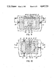
- FIG. 5 is a vertical cross-section through a telephone set base in which a circuit board, as in FIGS. 1 and 2, is mounted in a top housing 30. Also indicated are pushbuttons 31.
- the sub-assembly of the top housing, or cover, 30, is illustrated in FIG. 6.
- a position for lighted indicators is indicated at 35, housings 36 for pushbuttons, one pushbutton 31 being shown.
- a lighted indicator 29 is shown.
- Further elongate pushbuttons can be provided at positions 37.
- An elastomeric member 16, with switch members 17 and 18, and the circuit board 10 rest on the inner surface of the top housing, secured by screws, one illustrated at 38.
- the ringer is shown, comprising a speaker 39, a foam washer 40 and a housing 41.
- the ringer assembly is mounted against a grill 42 via brackets 43 having ribs 44 which interengage with protrusions 45 on the housing 41.
- a hook switch actuator 46 is mounted on the top housing and has a lever 47 which projects into the recess 48 which receives the transducer housing of the handset, the handset pushing on the arm to actuate the actuator.
- An arm 49 extends over the hook switch member 18 of the elastomeric member 16.
- a spring 50 biases the actuator 46.
- FIG. 7 illustrates the assembly of the various items in FIG. 6, omitting the elastomeric member 16 and board 10.
- FIG. 8 illustrates a typical telephone set 51 and the associated parts--bottom housing 31, top housing 30 with the various items and components mounted therein, and a handset 52.
- FIGS. 9, 10, 11 and 12 illustrate some forms, as an example.
- FIGS. 9 and 10 illustrate contact member arrangements in which contact members connected to two conductors are interleaved for interconnection by a further member
- FIGS. 11 and 12 illustrate contact member arrangements in which contact members are connected to four conductors.
- FIGS. 13 and 14 are cross-sections on FIGS. 9 and 10.
- FIG. 9 illustrates a simple arrangement, in which two conductors, 60 and 61, part of a circuit pattern as at 11 in FIG. 1, each end in an elongate pad 62 and 63.
- the conductors 60 and 61 and the pads 62 and 63 are typically of copper.
- Contact members extend from the pads 62 and 63 and have inter-digital finger-like members 64 and 65.
- the members 64 and 65 extend from elongate pads 66 and 67 extending over pads 62 and 63.
- the contact members comprising the members 64 and 65 and pads 66 and 67 are of carbon, formed by carbon ink deposited on the circuit board 10.
- the resist layer may be applied before or after deposition of the carbon ink.
- the resist layer can be applied before or after deposition of the carbon ink.
- the resist layer is applied before the carbon ink and in further patterns the resist layer is applied after the carbon ink.
- the resist layer, indicated at 68 can be applied before or after the carbon ink, and has been shown as applied after deposit of the carbon ink, the window periphery being seen at 69.
- FIG. 10 illustrates an arrangement or pattern in which two conductors 70 and 71 each have an elongate pad 72 and 73.
- Conductor 70 in this example is a continuous conductor with the pad 72 at an intermediate position.
- Conductors 70, 71 and pads 72 and 73 are again of copper and contact members having inter-digital members 74 and 75 extending from pads 76 and 77 extend from the conductors 70 and 71.
- the resist layer 68 is shown applied before the deposition of the carbon ink to form the members 74 and 75 and pads 76 and 77, although it can be applied after.
- FIG. 11 illustrates a more complex pattern of conductors and contact members.
- Each has an elongate pad 84, 85, 86 and 87.
- Conductors 80 and 82 are connected by a continuous contact member 92, of a sinuous or zig zag pattern, extending between pads 88 and 90. From pad 89 extend members 93 and from pad 91 extend members 94.
- Members 92, 93 and 94 form an inter-digital, or interleaved, pattern.
- the resist layer 68 is applied after deposition of the carbon ink.
- FIG. 12 is a further example of a more complex conductor and contact member pattern.
- the end of conductor 98 extends laterally to provide a wide connection portion 99.
- Carbon ink pads 100 and 101 and 102 are formed at the ends of the conductors 96, 97 and 98.
- Conductors 95 and 97 are connected by a contact member 104, which has a pad 101 at one end, for conductor 97, but merely overlaps the end of conductor 95.
- Pads 101 and 102 are formed over the ends of conductors 96 and 98 and contact members 108 and 109 extend from these pads.
- Contact member 104 is of sinuous form and contact members 108 and 109 are inter-digital, or interleaved, with contact member 104.
- the resist layer 68 is shown deposited after deposition of the carbon ink for pads 100, 101 and 102 and contact members 104, 108 and 109, but can be deposited before the carbon ink.
- Somewhat similar patterns as in FIGS. 11 and 12 can be used with these conductors.
- one of the conductors 81 and 83 or 96 and 98 can be omitted, together with the associated contact member, leaving a sinuous member 92 or 104 and one other contact member.
- FIGS. 13 and 14 cross-sections through the arrangements of FIGS. 9 and 10, illustrate the layer arrangements.
- the thickness of the layers, and particularly the relative thickness, are exaggerated and not to scale, to provide clarity.
- the particular pattern, or arrangement, of the carbon contact members and associated copper conductors can vary considerably.
- the copper conductors extend only to a peripheral area of a contact position where acceptable spacing can readily be provided. While a local enlargement or pad can be provided on a conductor, this is not essential.
- the contact members themselves are of carbon formed by depositing carbon ink, for example by screen printing. While a corresponding pad of carbon can be provided, over a copper pad, this also is not essential. In certain circumstances, however, the provision of pads on the conductor, contact members, or both, can provide a reduction in alignment requirements.
- the only alignment necessary is that between carbon ink and the conductor and the limitations at these positions are much less restrictive than are necessary when applying carbon ink over copper to form the actual inter-digital contact members.
- the contact member patterns are applied at one step, alignment between the two sets of inter-digital contact members is assured.
- very close spacing can be obtained.
- the inter-digital pattern, and close spacing is used to ensure good contact by a contact member such as a pushbutton, independent of any possible tilting of a pushbutton during operation.
Abstract
Description
Claims (14)
Applications Claiming Priority (1)
| Application Number | Priority Date | Filing Date | Title |
|---|---|---|---|
| CA000492244A CA1223081A (en) | 1985-10-04 | 1985-10-04 | Circuit board with contact positions, as used for telecommunications terminals and other apparatus |
Publications (1)
| Publication Number | Publication Date |
|---|---|
| US4647729A true US4647729A (en) | 1987-03-03 |
Family
ID=4131543
Family Applications (1)
| Application Number | Title | Priority Date | Filing Date |
|---|---|---|---|
| US06/785,114 Expired - Fee Related US4647729A (en) | 1985-10-04 | 1985-10-07 | Circuit board with contact positions, as used for telecommunications terminals and other apparatus |
Country Status (2)
| Country | Link |
|---|---|
| US (1) | US4647729A (en) |
| CA (1) | CA1223081A (en) |
Cited By (7)
| Publication number | Priority date | Publication date | Assignee | Title |
|---|---|---|---|---|
| EP0268497A2 (en) * | 1986-11-20 | 1988-05-25 | Brother Kogyo Kabushiki Kaisha | Printed circuit board |
| US4795861A (en) * | 1987-11-17 | 1989-01-03 | W. H. Brady Co. | Membrane switch element with coated spacer layer |
| US4857683A (en) * | 1988-12-28 | 1989-08-15 | W. H. Brady Co. | Membrane switchcores with key cell contact elements connected together for continuous path testing |
| EP0637830A2 (en) * | 1993-07-20 | 1995-02-08 | Fluke Corporation | Electrical switch having interdigitated and through poles |
| US5694124A (en) * | 1996-01-31 | 1997-12-02 | Texas Instruments Incorporated | Portable computer with integrated circuit board and keyboard |
| WO2002078411A1 (en) * | 2001-03-22 | 2002-10-03 | Siemens Aktiengesellschaft | Circuit support element for electronic devices, in particular for communication terminals |
| US20050109602A1 (en) * | 2003-11-20 | 2005-05-26 | Parkinson Joel K. | Elastomer keypad and bezel |
Citations (9)
| Publication number | Priority date | Publication date | Assignee | Title |
|---|---|---|---|---|
| US3504098A (en) * | 1965-02-03 | 1970-03-31 | Resources & Facilities Corp | Printed circuit panel |
| US3760137A (en) * | 1970-10-05 | 1973-09-18 | Alps Electric Co Ltd | Matrix push-button switch |
| US3860771A (en) * | 1973-10-29 | 1975-01-14 | Chomerics Inc | Keyboard switch assembly with dome shaped actuator having associated underlying contactor means |
| US4045636A (en) * | 1976-01-28 | 1977-08-30 | Bowmar Instrument Corporation | Keyboard switch assembly having printed circuit board with plural layer exposed contacts and undersurface jumper connections |
| US4296272A (en) * | 1979-11-30 | 1981-10-20 | Rca Corporation | Composite substrate |
| US4328399A (en) * | 1979-02-05 | 1982-05-04 | Northern Telecom Limited | Pushbutton switch assembly for telecommunications and other input |
| US4423294A (en) * | 1982-06-17 | 1983-12-27 | The Hall Company | Laminate switch assembly having improved durability |
| US4451714A (en) * | 1983-02-09 | 1984-05-29 | Eventoff Franklin Neal | Spacerless keyboard switch circuit assembly |
| US4527021A (en) * | 1981-07-15 | 1985-07-02 | Shin-Etsu Polmer Co., Ltd. | Keyboard switch assembly |
-
1985
- 1985-10-04 CA CA000492244A patent/CA1223081A/en not_active Expired
- 1985-10-07 US US06/785,114 patent/US4647729A/en not_active Expired - Fee Related
Patent Citations (9)
| Publication number | Priority date | Publication date | Assignee | Title |
|---|---|---|---|---|
| US3504098A (en) * | 1965-02-03 | 1970-03-31 | Resources & Facilities Corp | Printed circuit panel |
| US3760137A (en) * | 1970-10-05 | 1973-09-18 | Alps Electric Co Ltd | Matrix push-button switch |
| US3860771A (en) * | 1973-10-29 | 1975-01-14 | Chomerics Inc | Keyboard switch assembly with dome shaped actuator having associated underlying contactor means |
| US4045636A (en) * | 1976-01-28 | 1977-08-30 | Bowmar Instrument Corporation | Keyboard switch assembly having printed circuit board with plural layer exposed contacts and undersurface jumper connections |
| US4328399A (en) * | 1979-02-05 | 1982-05-04 | Northern Telecom Limited | Pushbutton switch assembly for telecommunications and other input |
| US4296272A (en) * | 1979-11-30 | 1981-10-20 | Rca Corporation | Composite substrate |
| US4527021A (en) * | 1981-07-15 | 1985-07-02 | Shin-Etsu Polmer Co., Ltd. | Keyboard switch assembly |
| US4423294A (en) * | 1982-06-17 | 1983-12-27 | The Hall Company | Laminate switch assembly having improved durability |
| US4451714A (en) * | 1983-02-09 | 1984-05-29 | Eventoff Franklin Neal | Spacerless keyboard switch circuit assembly |
Cited By (12)
| Publication number | Priority date | Publication date | Assignee | Title |
|---|---|---|---|---|
| EP0268497A2 (en) * | 1986-11-20 | 1988-05-25 | Brother Kogyo Kabushiki Kaisha | Printed circuit board |
| EP0268497A3 (en) * | 1986-11-20 | 1989-02-08 | Brother Kogyo Kabushiki Kaisha | Printed circuit board |
| US4795861A (en) * | 1987-11-17 | 1989-01-03 | W. H. Brady Co. | Membrane switch element with coated spacer layer |
| US4857683A (en) * | 1988-12-28 | 1989-08-15 | W. H. Brady Co. | Membrane switchcores with key cell contact elements connected together for continuous path testing |
| EP0375832A2 (en) * | 1988-12-28 | 1990-07-04 | W.H. Brady Co. | Membrane switchcores with key cell contact elements connected together for continuous path testing |
| EP0375832A3 (en) * | 1988-12-28 | 1991-09-11 | W.H. Brady Co. | Membrane switchcores with key cell contact elements connected together for continuous path testing |
| EP0637830A2 (en) * | 1993-07-20 | 1995-02-08 | Fluke Corporation | Electrical switch having interdigitated and through poles |
| EP0637830A3 (en) * | 1993-07-20 | 1995-06-14 | Fluke Corp | Electrical switch having interdigitated and through poles. |
| US5694124A (en) * | 1996-01-31 | 1997-12-02 | Texas Instruments Incorporated | Portable computer with integrated circuit board and keyboard |
| WO2002078411A1 (en) * | 2001-03-22 | 2002-10-03 | Siemens Aktiengesellschaft | Circuit support element for electronic devices, in particular for communication terminals |
| US20050109602A1 (en) * | 2003-11-20 | 2005-05-26 | Parkinson Joel K. | Elastomer keypad and bezel |
| US7087847B2 (en) * | 2003-11-20 | 2006-08-08 | White Electronic Designs Corporation | Elastomer keypad and bezel |
Also Published As
| Publication number | Publication date |
|---|---|
| CA1223081A (en) | 1987-06-16 |
Similar Documents
| Publication | Publication Date | Title |
|---|---|---|
| US4180711A (en) | Desk-top calculator keyboard switch | |
| US6148183A (en) | Switch assembly for an electronic device | |
| US20140144765A1 (en) | Pcb tact switch | |
| DE60028107T2 (en) | Portable telephone device | |
| US4647729A (en) | Circuit board with contact positions, as used for telecommunications terminals and other apparatus | |
| US4328399A (en) | Pushbutton switch assembly for telecommunications and other input | |
| US3210484A (en) | Push button device | |
| US4243846A (en) | Pushbutton switch assembly for telecommunications and other input apparatus | |
| EP0088211A1 (en) | Switching contact | |
| EP0531973B1 (en) | Click-action membrane switch | |
| US4539445A (en) | Click disc switch assembly | |
| JP2000092174A (en) | Portable telephone set | |
| JP2643239B2 (en) | Plastic contact spring | |
| CA1100165A (en) | Pushbutton switch assembly for telecommunications and other input apparatus | |
| US7183634B2 (en) | Printed circuit board tact switch | |
| GB2255688A (en) | Telephone station set with flexible and rigid circuit boards | |
| CA1225762A (en) | Telephone hook switch with elastomeric contact member | |
| CA2065988A1 (en) | Telephone station set with flexible and rigid circuit boards | |
| CA1137649A (en) | Electrical circuit on porcelain coated metal substrate | |
| JP3538030B2 (en) | Switch structure and switch plate | |
| JPH10233141A (en) | Switch and its layout structure | |
| JP3780961B2 (en) | Electrical connection device and electrical connection method for flat flexible circuit board | |
| US4710954A (en) | Telephone set line switch | |
| CA1268571A (en) | Dial assembly for telephone sets | |
| GB2201063A (en) | Telephone switch hooks |
Legal Events
| Date | Code | Title | Description |
|---|---|---|---|
| AS | Assignment |
Owner name: NORTHERN TELECOM LIMITED, P.O. BOX 6123, STATION " Free format text: ASSIGNMENT OF ASSIGNORS INTEREST.;ASSIGNORS:COLLAR, GEOFFREY A.;MOSS, JOHN S.;CHU, PAK-JONG;REEL/FRAME:004468/0631 Effective date: 19850912 Owner name: NORTHERN TELECOM LIMITED, P.O. BOX 6123, STATION " Free format text: ASSIGNMENT OF ASSIGNORS INTEREST.;ASSIGNOR:BELL-NORTHERN RESEARCH LTD.;REEL/FRAME:004468/0634 Effective date: 19850912 Owner name: NOTHERN TELECOM LIMITED, P.O. BOX 6123, STATION "A Free format text: ASSIGNMENT OF ASSIGNORS INTEREST.;ASSIGNOR:BELL NORTHERN RESEARCH LTD.;REEL/FRAME:004468/0632 Effective date: 19850912 Owner name: NORTHERN TELECOM LIMITED, P.O. BOX 6123, STATION " Free format text: ASSIGNMENT OF ASSIGNORS INTEREST.;ASSIGNORS:MC DONALD, PAUL D.;VOSS, BRIAN E.;REEL/FRAME:004468/0633 Effective date: 19850912 |
|
| REMI | Maintenance fee reminder mailed | ||
| LAPS | Lapse for failure to pay maintenance fees | ||
| STCH | Information on status: patent discontinuation |
Free format text: PATENT EXPIRED DUE TO NONPAYMENT OF MAINTENANCE FEES UNDER 37 CFR 1.362 |
|
| FP | Lapsed due to failure to pay maintenance fee |
Effective date: 19910303 |